US6667806B2 - Process and apparatus for manufacturing semiconductor device - Google Patents
Process and apparatus for manufacturing semiconductor device Download PDFInfo
- Publication number
- US6667806B2 US6667806B2 US09/796,613 US79661301A US6667806B2 US 6667806 B2 US6667806 B2 US 6667806B2 US 79661301 A US79661301 A US 79661301A US 6667806 B2 US6667806 B2 US 6667806B2
- Authority
- US
- United States
- Prior art keywords
- pattern
- patterns
- positional difference
- light
- wavelength
- Prior art date
- Legal status (The legal status is an assumption and is not a legal conclusion. Google has not performed a legal analysis and makes no representation as to the accuracy of the status listed.)
- Expired - Lifetime, expires
Links
- 239000004065 semiconductor Substances 0.000 title claims abstract description 22
- 238000000034 method Methods 0.000 title claims description 25
- 238000004519 manufacturing process Methods 0.000 title claims description 16
- 238000012937 correction Methods 0.000 claims abstract description 8
- 239000000758 substrate Substances 0.000 claims description 14
- 238000012545 processing Methods 0.000 claims description 10
- 238000003384 imaging method Methods 0.000 claims description 7
- 230000001678 irradiating effect Effects 0.000 claims description 6
- 238000001228 spectrum Methods 0.000 claims description 3
- 230000000737 periodic effect Effects 0.000 claims 2
- 230000004075 alteration Effects 0.000 abstract 2
- 230000007423 decrease Effects 0.000 abstract 1
- 230000003287 optical effect Effects 0.000 description 16
- 239000011295 pitch Substances 0.000 description 10
- 230000010363 phase shift Effects 0.000 description 9
- XUIMIQQOPSSXEZ-UHFFFAOYSA-N Silicon Chemical compound [Si] XUIMIQQOPSSXEZ-UHFFFAOYSA-N 0.000 description 5
- 238000009826 distribution Methods 0.000 description 5
- 238000005530 etching Methods 0.000 description 4
- 230000009466 transformation Effects 0.000 description 4
- 239000003795 chemical substances by application Substances 0.000 description 3
- 238000010586 diagram Methods 0.000 description 3
- 230000010287 polarization Effects 0.000 description 3
- 230000003595 spectral effect Effects 0.000 description 3
- 238000001514 detection method Methods 0.000 description 2
- 238000011161 development Methods 0.000 description 2
- 229920002120 photoresistant polymer Polymers 0.000 description 2
- 229910052710 silicon Inorganic materials 0.000 description 2
- 239000010703 silicon Substances 0.000 description 2
- 238000012935 Averaging Methods 0.000 description 1
- 238000004364 calculation method Methods 0.000 description 1
- 230000001427 coherent effect Effects 0.000 description 1
- 230000007547 defect Effects 0.000 description 1
- 230000002950 deficient Effects 0.000 description 1
- 238000010894 electron beam technology Methods 0.000 description 1
- 238000009434 installation Methods 0.000 description 1
- 238000002955 isolation Methods 0.000 description 1
- 239000002184 metal Substances 0.000 description 1
- 238000004088 simulation Methods 0.000 description 1
Images


Classifications
-
- G—PHYSICS
- G03—PHOTOGRAPHY; CINEMATOGRAPHY; ANALOGOUS TECHNIQUES USING WAVES OTHER THAN OPTICAL WAVES; ELECTROGRAPHY; HOLOGRAPHY
- G03F—PHOTOMECHANICAL PRODUCTION OF TEXTURED OR PATTERNED SURFACES, e.g. FOR PRINTING, FOR PROCESSING OF SEMICONDUCTOR DEVICES; MATERIALS THEREFOR; ORIGINALS THEREFOR; APPARATUS SPECIALLY ADAPTED THEREFOR
- G03F7/00—Photomechanical, e.g. photolithographic, production of textured or patterned surfaces, e.g. printing surfaces; Materials therefor, e.g. comprising photoresists; Apparatus specially adapted therefor
- G03F7/70—Microphotolithographic exposure; Apparatus therefor
- G03F7/70483—Information management; Active and passive control; Testing; Wafer monitoring, e.g. pattern monitoring
- G03F7/70605—Workpiece metrology
- G03F7/70616—Monitoring the printed patterns
- G03F7/70633—Overlay, i.e. relative alignment between patterns printed by separate exposures in different layers, or in the same layer in multiple exposures or stitching
-
- H—ELECTRICITY
- H01—ELECTRIC ELEMENTS
- H01L—SEMICONDUCTOR DEVICES NOT COVERED BY CLASS H10
- H01L22/00—Testing or measuring during manufacture or treatment; Reliability measurements, i.e. testing of parts without further processing to modify the parts as such; Structural arrangements therefor
- H01L22/20—Sequence of activities consisting of a plurality of measurements, corrections, marking or sorting steps
-
- H—ELECTRICITY
- H01—ELECTRIC ELEMENTS
- H01L—SEMICONDUCTOR DEVICES NOT COVERED BY CLASS H10
- H01L2924/00—Indexing scheme for arrangements or methods for connecting or disconnecting semiconductor or solid-state bodies as covered by H01L24/00
- H01L2924/0001—Technical content checked by a classifier
- H01L2924/0002—Not covered by any one of groups H01L24/00, H01L24/00 and H01L2224/00
Definitions
- the present invention relates to a process for manufacturing a semiconductor device and in particular to a method and apparatus for detecting and correcting the alignment error at a high precision in an exposure step and a process for manufacturing a semiconductor device based upon a result of the correction of the alignment error.
- the process for manufacturing a semiconductor device is conducted by repeating on each layer the steps of forming a layer on a wafer; applying a photoresist which is a photosensitive agent upon the formed layer; exposing the resist with a circuit pattern on a reticle and developing it; and then forming the circuit pattern on the wafer by etching away the layer. If there is a difference of the position of the circuit pattern on exposure relative to an underlaying layer pattern in this manufacturing process, the circuit may then be broken or short-circuited, resulting in an defective semiconductor device.
- the relative difference in position between a registering mark which is formed of the resist after the development and an alignment mark on the underlaying layer is automatically measured by means of an optical microscope and the difference in position is fed back to an exposure apparatus at subsequent exposing step.
- the alignment mark is usually provided in a region at the edge of an exposure area in which no circuit pattern is provided.
- the alignment mark is formed at a line width of 2 to 4 ⁇ m, which is larger in comparison with the circuit line width so that it can be resolved by an optical detecting method.
- the present inventors have found that following problems which have not heretofore been considered will occur since a tolerable error in alignment is about 30 nm for DRAMs having a line width of 0.1 ⁇ m which will be developed in the future.
- a first problem resides in an error of writing using a reticle.
- the pattern on the reticle is scanned by means of an electron beam scanning apparatus.
- the error in position of scanning is about 50 nm on the reticle.
- the error is about 10 nm on the wafer, which is not negligible for the tolerable error of 30 nm.
- the shift of the alignment mark at the edge of the exposure area does not necessarily match with that of the circuit at the exposure area.
- a second problem resides in the distortion of a projecting lens of the exposure apparatus. Since the image of the reticle which is transferred upon the wafer by means of the projecting lens also has a distortion of about 10 nm, this also causes the mismatch of the alignment error of the alignment mark with the circuit.
- the present invention provides a process for measuring the alignment error at the step for exposing a semiconductor with light in which the underlaying layer pattern is not exposed on the surface in the circuit area.
- a process for manufacturing a semiconductor device comprises the steps of:
- the process for manufacturing a semiconductor device is characterized in that light which is detected at the steps for detecting said first and second images is polarized in a direction parallel with the longitudinal directions of said first and second patterns.
- the process for manufacturing a semiconductor device is characterized in that said first and second patterns are a plurality of patterns having the same pitch.
- the process for manufacturing a semiconductor device is characterized in that said step for calculating the relative positional difference between said first and second images calculates the phase at a frequency corresponding to the maximum spectrum which is obtained by Fourier-transforming the images of said plurality of patterns in a direction in which said plurality of patterns are arrayed so that the relative positional difference is calculated from the calculated phase.
- the average relative positional error between said first and second patterns in said plurality of patterns can be achieved at high speed and high accuracy.
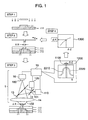
- FIG. 1 is a diagram explaining the flow of the process for manufacturing a semiconductor device of the present invention
- FIG. 2 is a sectional view of the semiconductor device explaining a first and second patterns comprising a plurality of line patterns, the alignment error of which is to be calculated in accordance with the present invention
- FIG. 3 is a diagram explaining an optical image of the second pattern
- FIG. 4 is a graph explaining the relation between the phase and the alignment error of the optical image at a wavelength of 266 nm;
- FIG. 5 is a graph explaining the relation between the phase and the alignment error of the optical image at a wavelength of 308 nm;
- FIG. 6 is a graph explaining the relation between the phase and the alignment error of the optical image at a wavelengths of 266 and 308 nm;
- FIG. 7 is a diagram explaining the flow for calculating the phase of the optical image
- FIG. 8 is a graph showing the contrast characteristics for the pattern special frequency of an objective lens
- FIG. 9 is a substantial front view showing an optical system for detecting the image with light which is polarized in parallel with the longitudinal direction of the pattern and a graph showing the distribution of the light strength of the detecting image;
- FIG. 10 is a substantial front view showing an optical system for detecting the image with light which is polarized in a direction normal to the longitudinal direction of the pattern and a graph showing the distribution of the light strength of the detecting image;
- FIG. 11 is a substantial front view of the optical system explaining one embodiment for selecting light which is polarized in a direction normal to the longitudinal direction of the pattern.
- FIG. 12 is a substantial front view of the optical system explaining another embodiment for selecting light which is polarized in a direction normal to the longitudinal direction of the pattern.
- FIG. 1 An embodiment of a process for manufacturing a semiconductor device in accordance with the present invention will be described with reference to FIG. 1 .
- a first pattern 21 is formed by developing and etching the exposed photosensitive agent on a substrate 210 after it is exposed to light by means of an illustrated exposing apparatus.
- a second pattern 22 is formed by a process as follows: After an oxide layer 221 is formed on the first pattern 21 , it is polished. After an oxide layer 222 is formed, a photosenitive agent on the substrate is exposed to light, and it is developed and etched.
- an image 2210 of the second pattern 22 is picked up by means of an alignment error measuring apparatus 1 .
- a control and processing unit 10 turns on a light source 110 for emitting light having a first wavelength.
- Light 101 which is emitted from the light source 110 of the first wavelength is transmitted through a beam splitter 12 and is reflected on a beam splitter 13 and is projected on the device to form a second pattern thereon via an objective lens 14 .
- the reflected light 102 of the second pattern 22 is imaged upon an image pick up surface 160 of an imaging device 16 via the objective lens 14 and beam splitter 13 .
- An image 2210 of the second pattern of the light having the first wave length is processed by the control and processing unit 10 so that the center position 1100 is calculated.
- the control and processing unit 10 turns off the light source 110 of the first wavelength and turns on the light source 120 of second wave length.
- Light having the second wavelength travels through the same optical path along which the light 101 emitted from the above-mentioned light source of the first wavelength travels so that a second pattern of the light having the second wavelength is imaged upon the image pick up surface of the imaging device 16 .
- the image 2220 of the second pattern of the second wavelength light is processed by the control and processing unit 10 so that a central position 1200 is calculated.
- the control and processing unit 10 turns off the light source 11 of the first wave-length and turns on the light source 120 of second wave length.
- Light having the second wave length travels through the same optical path along which the light 101 emitted from the above-mentioned light source of the first wave length travels so that a second pattern of the light having the second wave length is imaged upon the image pick up surface of the imaging device 16 .
- the image 2220 of the second pattern of the second wave length light is processed by the control and processing unit 10 so that a central position 1200 is calculated.
- the control and processing unit computes the difference ⁇ between the center position 1100 of the second pattern image of the first wavelength light and the center position 1200 of the second pattern image of the second wavelength light. If the first and second patterns are detected as a plurality of line patterns having equal pitches, the difference ⁇ could be calculated as an average of the misalignment of the plurality of patterns. The alignment accuracy can be enhanced by the averaging. Since transistors are disposed at equal pitch, the pitch of the first pattern is usually equal to that of the second pattern. It is possible to detect these patterns as plural line patterns having equal pitches.
- the alignment error ⁇ x is calculated in accordance with the relation 1300 between the preliminarily determined difference between the center positions of the second pattern images of the first and second wavelength lights and the alignment error between the first and second patterns.
- the ⁇ x is fed back to the exposing apparatus as an alignment error correction value when the second pattern is projected at next step 2 .
- the exposing apparatus exposes the second pattern upon a new substrate on which the first pattern is formed and a photoresist is applied.
- the second pattern, the alignment error of which has been corrected relative to the first pattern can be formed on the substrate by conducting the development and etching of the substrate to which the second pattern is exposed.
- the first and second patterns are assumed to be a plurality of line patterns having equal pitches.
- the first pattern is a stepped pattern of silicon 210 .
- An isolation pattern having a width of 0.15 ⁇ m is formed by flattening a recess with an oxide layer 221 .
- the second pattern have grooves in an oxide layer 222 having a width of 0.08 ⁇ m for forming metal gates.
- Pitch is assumed to be 0.3 ⁇ m.
- the optical resolution R( ⁇ m) of the pattern is defined as follows:
- NA denotes the aperture ratio of the objective lens 14 .
- the line width of the second pattern which is 0.08 ⁇ m is less than the resolution.
- the light strength distribution 2211 of the image if only the second pattern 22 should be formed on the silicon 210 is a cosine wave so that the second pattern is not resolved.
- both of the images of the first and second patterns 21 and 22 are cosine waves, so that the resultant image of the first and second images is obtained on the image pick up surface 160 .
- the images of the first pattern 21 is represented as follows: A ⁇ ⁇ cos ⁇ ( 2 ⁇ ⁇ ⁇ x P ) ( 2 )
- the image of the second pattern 22 which is shifted by relative to the first pattern 21 is represented as follows: B ⁇ ⁇ cos ⁇ ( 2 ⁇ ⁇ ⁇ ⁇ x + ⁇ ⁇ ⁇ x P ) ( 3 )
- X denotes a coordinate on the image pick up surface 160 and P denotes the pitch of the first and second patterns.
- C and D denotes constants, which are represented by equations (6) and (6), respectively.
- C A + B ⁇ ⁇ cos ⁇ ( 2 ⁇ ⁇ ⁇ ⁇ ⁇ ⁇ ⁇ x P ) ( 5 )
- D B ⁇ ⁇ sin ⁇ ( 2 ⁇ ⁇ ⁇ ⁇ ⁇ ⁇ ⁇ ⁇ x P ) ( 6 )
- the resultant image is a sinusoidal wave having a phase shift ⁇ relative to the first pattern 21 . Accordingly, it is possible to calculate the alignment error ⁇ X from the phase shift ⁇ if the relation between the alignment ⁇ X error and the phase shift ⁇ is preliminarily determined.
- the first and second patterns 21 and 22 is formed by projecting light having a second wavelength which is different from that of the first wavelength.
- the phase shift ⁇ ′ of the image on the image pick up surface 160 at this time is determined.
- the relation between the phase shift ⁇ ′ and ⁇ x at the second wavelength is different from that at the first wavelength.
- FIGS. 4 and 5 show the result of the relations between the phase shifts ⁇ , ⁇ ′ and the alignment error ⁇ x using wavelengths 266 nm of the biquadratic harmonic of YAG laser and 308 nm of XeCL eximer laser, which are obtained by wave optics simulation.
- FIG. 6 shows the relation between shift difference ⁇ and ⁇ x.
- phase ⁇ is calculated in accordance with (7).
- ⁇ tan - 1 ⁇ ( Sm Cm ) ( 7 )
- Sm denotes a constant of sine wave after the Fourier transformation corresponding to the maximum spectral frequency
- Cm denotes a constant of the cosine wave after the Fourier transformation corresponding to the maximum spectral frequency.
- the image of the plurality of line patterns be substantially cosine waves.
- the objective lens 14 will not transmit the second or more-order diffracted light from the plurality of line patterns, but the first-order diffracted light.
- FIG. 7 shows the relation between the spacial frequency of the pattern and the image contrast when coherent imaging (imaging of illuminating light in which the aperture ratio of NA of an illuminating system to that of the objective lens is one or more) is conducted by means of the objective lens 14 .
- NA denotes the aperture ratio of the objective lens and denotes the wavelength of illuminating light. Accordingly, the requirement that the objective lens will not transmit the above-mentioned second-order or more diffracted light, but the first-order diffracted light is that the reference frequency of the pattern is not higher than the cut off frequency exceeds fc and is given as follows: 1 P ⁇ 2 ⁇ NA ⁇ ⁇ 2 P ( 9 )
- P denotes the pitch of the pattern.
- 1/P 3.33 (1/ ⁇ m)
- 2/P 6.67 (1/ ⁇ m).
- FIG. 9 shows the pattern image 2212 when the image of the pattern 23 is detected with light which is polarized in parallel with the longitudinal direction of the pattern.
- the polarization direction of the zero-order, minus first-order and first order lights 1000 , 1001 and 1002 , on the image pick up surface 160 , respectively are normal to the paper of the drawing. Interference of these lights to each other provides an excellent image contrast. If the detection is conducted with light which is polarized in a direction perpendicular to the longitudinal direction of the pattern as shown in FIG.
- the zero-order, minus first-order and first-order diffracted lights 1010 , 1011 and 1012 are not same on the image pick up surface 160 .
- the minus first-order diffracted light 1011 and the first-order diffracted light 1012 which contribute to the interference becomes sinusoidal components, so that the contrast of the pattern image 2213 is lowered. Accordingly, the contrast of the pattern image is enhanced by detecting it with only light which is polarized in a direction in parallel with the longitudinal direction of the pattern.
- a polarization element 191 which transmits only light which is polarized in the longitudinal direction of the pattern (direction normal to the paper of the drawing) is disposed in front of the imaging device 16 .
- polarization elements 192 and 193 which transmit only light which is polarized in the longitudinal direction of the pattern (direction normal to the paper) are disposed on the exit side of the light sources 110 and 120 , respectively.
- the installation direction of the light source 110 or 120 may be matched with the longitudinal direction of the pattern if the light source 110 or 120 emits linearly polarized light such as laser.
- the alignment error between a real pattern in a circuit of the semiconductor device and the underlaying pattern can be measured by using the real pattern in the circuit of the semiconductor device rather than the alignment mark at the exposed area edge in the above-mentioned embodiments, it is possible to measure the real alignment error of the circuit pattern, including the reticle writing error and the lens distortion. This enables a proper correction value which will not cause any defect in the circuit pattern to be fed back to the exposing apparatus, contributing to an enhancement in the yield of the future semiconductor device having the size of 0.1 ⁇ m or less.
Abstract
Description


Claims (8)
Applications Claiming Priority (2)
| Application Number | Priority Date | Filing Date | Title |
|---|---|---|---|
| JP2000-283776 | 2000-09-13 | ||
| JP2000283776A JP3892656B2 (en) | 2000-09-13 | 2000-09-13 | Alignment error measuring apparatus and semiconductor device manufacturing method using the same |
Publications (2)
| Publication Number | Publication Date |
|---|---|
| US20020048020A1 US20020048020A1 (en) | 2002-04-25 |
| US6667806B2 true US6667806B2 (en) | 2003-12-23 |
Family
ID=18768085
Family Applications (1)
| Application Number | Title | Priority Date | Filing Date |
|---|---|---|---|
| US09/796,613 Expired - Lifetime US6667806B2 (en) | 2000-09-13 | 2001-03-02 | Process and apparatus for manufacturing semiconductor device |
Country Status (2)
| Country | Link |
|---|---|
| US (1) | US6667806B2 (en) |
| JP (1) | JP3892656B2 (en) |
Cited By (5)
| Publication number | Priority date | Publication date | Assignee | Title |
|---|---|---|---|---|
| US20040002172A1 (en) * | 2002-06-26 | 2004-01-01 | Doo-Hoon Goo | Methods and apparatus for aligning a wafer in which multiple light beams are used to scan alignment marks |
| US20050051721A1 (en) * | 2003-06-27 | 2005-03-10 | Kenji Watanabe | Sample dimension-measuring method and charged particle beam apparatus |
| US20110089346A1 (en) * | 2009-10-21 | 2011-04-21 | Nuflare Technology, Inc. | Method and system for pattern writing with charged-particle beam |
| US9262819B1 (en) * | 2014-09-26 | 2016-02-16 | GlobalFoundries, Inc. | System and method for estimating spatial characteristics of integrated circuits |
| US20160300338A1 (en) * | 2015-04-13 | 2016-10-13 | Anchor Semiconductor Inc. | Pattern weakness and strength detection and tracking during a semiconductor device fabrication process |
Families Citing this family (7)
| Publication number | Priority date | Publication date | Assignee | Title |
|---|---|---|---|---|
| US7310437B2 (en) * | 2000-03-08 | 2007-12-18 | Fujifilm Corporation | Image processing method and system, and storage medium |
| KR20050026088A (en) * | 2002-08-01 | 2005-03-14 | 몰레큘러 임프린츠 인코퍼레이티드 | Scatterometry alignment for imprint lithography |
| US7935545B2 (en) * | 2007-03-30 | 2011-05-03 | Tokyo Electron Limited | Method and apparatus for performing a site-dependent dual patterning procedure |
| JP2012164811A (en) * | 2011-02-07 | 2012-08-30 | Toshiba Corp | Method of manufacturing semiconductor device, method of determining shipping of exposure mask and method of manufacturing exposure mask |
| US9349660B2 (en) * | 2011-12-01 | 2016-05-24 | Taiwan Semiconductor Manufacturing Company, Ltd. | Integrated circuit manufacturing tool condition monitoring system and method |
| CN106647180B (en) * | 2016-11-28 | 2018-09-28 | 湖北凯昌光电科技有限公司 | Error correction and compensation method based on scaling board in direct write exposure machine |
| US11022877B2 (en) * | 2017-03-13 | 2021-06-01 | Applied Materials, Inc. | Etch processing system having reflective endpoint detection |
Citations (18)
| Publication number | Priority date | Publication date | Assignee | Title |
|---|---|---|---|---|
| US3712740A (en) * | 1969-04-19 | 1973-01-23 | K Hennings | Method for the automatic alignment of two articles to be brought into register with one another |
| US4741622A (en) * | 1985-03-04 | 1988-05-03 | Nippon Kogaku K.K. | Method and apparatus for detecting diversion |
| US4901109A (en) * | 1986-03-10 | 1990-02-13 | Canon Kabushiki Kaisha | Alignment and exposure apparatus |
| US5272501A (en) * | 1991-08-28 | 1993-12-21 | Nikon Corporation | Projection exposure apparatus |
| US5333050A (en) * | 1990-03-27 | 1994-07-26 | Canon Kabushiki Kaisha | Measuring method and apparatus for meausring the positional relationship of first and second gratings |
| US5402205A (en) * | 1992-12-21 | 1995-03-28 | Ultratech Stepper, Inc. | Alignment system for a Half-Field Dyson projection system |
| US5585923A (en) * | 1992-11-14 | 1996-12-17 | Canon Kabushiki Kaisha | Method and apparatus for measuring positional deviation while correcting an error on the basis of the error detection by an error detecting means |
| US5682239A (en) * | 1994-09-19 | 1997-10-28 | Canon Kabushiki Kaisha | Apparatus for detecting positional deviation of diffraction gratings on a substrate by utilizing optical heterodyne interference of light beams incident on the gratings from first and second light emitters |
| US5684565A (en) * | 1993-09-10 | 1997-11-04 | Hitachi, Ltd. | Pattern detecting method, pattern detecting apparatus, projection exposing apparatus using the same and exposure system |
| US5795687A (en) * | 1995-02-24 | 1998-08-18 | Nikon Corporation | Projection exposure method and alignment |
| US5850279A (en) * | 1995-03-23 | 1998-12-15 | Nikon Corporation | Alignment method, projection exposure method, and projection exposure apparatus |
| US6023321A (en) * | 1996-03-11 | 2000-02-08 | Nikon Corporation | Projection exposure apparatus and method |
| US6079256A (en) * | 1996-07-12 | 2000-06-27 | Kla Instruments Corporation | Overlay alignment measurement of wafers |
| US6100987A (en) * | 1994-03-25 | 2000-08-08 | Nikon Corporation | Position detecting apparatus |
| US6166801A (en) * | 1998-07-14 | 2000-12-26 | Nova Measuring Instruments, Ltd. | Monitoring apparatus and method particularly useful in photolithographically processing substrates |
| US6218200B1 (en) * | 2000-07-14 | 2001-04-17 | Motorola, Inc. | Multi-layer registration control for photolithography processes |
| US6297876B1 (en) * | 1997-03-07 | 2001-10-02 | Asm Lithography B.V. | Lithographic projection apparatus with an alignment system for aligning substrate on mask |
| US6356343B1 (en) * | 1996-11-07 | 2002-03-12 | Nikon Corporation | Mark for position detection and mark detecting method and apparatus |
-
2000
- 2000-09-13 JP JP2000283776A patent/JP3892656B2/en not_active Expired - Fee Related
-
2001
- 2001-03-02 US US09/796,613 patent/US6667806B2/en not_active Expired - Lifetime
Patent Citations (18)
| Publication number | Priority date | Publication date | Assignee | Title |
|---|---|---|---|---|
| US3712740A (en) * | 1969-04-19 | 1973-01-23 | K Hennings | Method for the automatic alignment of two articles to be brought into register with one another |
| US4741622A (en) * | 1985-03-04 | 1988-05-03 | Nippon Kogaku K.K. | Method and apparatus for detecting diversion |
| US4901109A (en) * | 1986-03-10 | 1990-02-13 | Canon Kabushiki Kaisha | Alignment and exposure apparatus |
| US5333050A (en) * | 1990-03-27 | 1994-07-26 | Canon Kabushiki Kaisha | Measuring method and apparatus for meausring the positional relationship of first and second gratings |
| US5272501A (en) * | 1991-08-28 | 1993-12-21 | Nikon Corporation | Projection exposure apparatus |
| US5585923A (en) * | 1992-11-14 | 1996-12-17 | Canon Kabushiki Kaisha | Method and apparatus for measuring positional deviation while correcting an error on the basis of the error detection by an error detecting means |
| US5402205A (en) * | 1992-12-21 | 1995-03-28 | Ultratech Stepper, Inc. | Alignment system for a Half-Field Dyson projection system |
| US5684565A (en) * | 1993-09-10 | 1997-11-04 | Hitachi, Ltd. | Pattern detecting method, pattern detecting apparatus, projection exposing apparatus using the same and exposure system |
| US6100987A (en) * | 1994-03-25 | 2000-08-08 | Nikon Corporation | Position detecting apparatus |
| US5682239A (en) * | 1994-09-19 | 1997-10-28 | Canon Kabushiki Kaisha | Apparatus for detecting positional deviation of diffraction gratings on a substrate by utilizing optical heterodyne interference of light beams incident on the gratings from first and second light emitters |
| US5795687A (en) * | 1995-02-24 | 1998-08-18 | Nikon Corporation | Projection exposure method and alignment |
| US5850279A (en) * | 1995-03-23 | 1998-12-15 | Nikon Corporation | Alignment method, projection exposure method, and projection exposure apparatus |
| US6023321A (en) * | 1996-03-11 | 2000-02-08 | Nikon Corporation | Projection exposure apparatus and method |
| US6079256A (en) * | 1996-07-12 | 2000-06-27 | Kla Instruments Corporation | Overlay alignment measurement of wafers |
| US6356343B1 (en) * | 1996-11-07 | 2002-03-12 | Nikon Corporation | Mark for position detection and mark detecting method and apparatus |
| US6297876B1 (en) * | 1997-03-07 | 2001-10-02 | Asm Lithography B.V. | Lithographic projection apparatus with an alignment system for aligning substrate on mask |
| US6166801A (en) * | 1998-07-14 | 2000-12-26 | Nova Measuring Instruments, Ltd. | Monitoring apparatus and method particularly useful in photolithographically processing substrates |
| US6218200B1 (en) * | 2000-07-14 | 2001-04-17 | Motorola, Inc. | Multi-layer registration control for photolithography processes |
Non-Patent Citations (1)
| Title |
|---|
| J. Allgair et al., Characterization of Overlay Tolerance Requirements for Via to Metal Alignment, SPIE Conference on Metrology, Inspection, and Process Control for Microlithography XIII, Santa Clara, CA, Mar. 1999, SPIE vol. 3677, pp. 239-247. |
Cited By (9)
| Publication number | Priority date | Publication date | Assignee | Title |
|---|---|---|---|---|
| US20040002172A1 (en) * | 2002-06-26 | 2004-01-01 | Doo-Hoon Goo | Methods and apparatus for aligning a wafer in which multiple light beams are used to scan alignment marks |
| US7068371B2 (en) * | 2002-06-26 | 2006-06-27 | Samsung Electronics Co., Ltd. | Methods and apparatus for aligning a wafer in which multiple light beams are used to scan alignment marks |
| US20050051721A1 (en) * | 2003-06-27 | 2005-03-10 | Kenji Watanabe | Sample dimension-measuring method and charged particle beam apparatus |
| US7476856B2 (en) * | 2003-06-27 | 2009-01-13 | Hitachi High-Technologies Corporation | Sample dimension-measuring method and charged particle beam apparatus |
| US20110089346A1 (en) * | 2009-10-21 | 2011-04-21 | Nuflare Technology, Inc. | Method and system for pattern writing with charged-particle beam |
| US9262819B1 (en) * | 2014-09-26 | 2016-02-16 | GlobalFoundries, Inc. | System and method for estimating spatial characteristics of integrated circuits |
| US20160300338A1 (en) * | 2015-04-13 | 2016-10-13 | Anchor Semiconductor Inc. | Pattern weakness and strength detection and tracking during a semiconductor device fabrication process |
| US9846934B2 (en) * | 2015-04-13 | 2017-12-19 | Anchor Semiconductor Inc. | Pattern weakness and strength detection and tracking during a semiconductor device fabrication process |
| US10062160B2 (en) | 2015-04-13 | 2018-08-28 | Anchor Semiconductor Inc. | Pattern weakness and strength detection and tracking during a semiconductor device fabrication process |
Also Published As
| Publication number | Publication date |
|---|---|
| US20020048020A1 (en) | 2002-04-25 |
| JP2002093689A (en) | 2002-03-29 |
| JP3892656B2 (en) | 2007-03-14 |
Similar Documents
| Publication | Publication Date | Title |
|---|---|---|
| US7643961B2 (en) | Position detecting device and position detecting method | |
| US7236244B1 (en) | Alignment target to be measured with multiple polarization states | |
| KR100255399B1 (en) | Condition optimization method for measuring overlay accuracy of pattern | |
| US6982793B1 (en) | Method and apparatus for using an alignment target with designed in offset | |
| JP4789393B2 (en) | Overlapping alignment mark design | |
| JP4150256B2 (en) | Method for measuring the alignment of a substrate with respect to a reference alignment mark | |
| US7046361B1 (en) | Positioning two elements using an alignment target with a designed offset | |
| JP3249154B2 (en) | Lateral position measuring apparatus and method in proximity lithographic system | |
| US20090195768A1 (en) | Alignment Mark and a Method of Aligning a Substrate Comprising Such an Alignment Mark | |
| JP2004279405A (en) | Device inspection | |
| KR20020079918A (en) | Method of measuring overlay | |
| US6667806B2 (en) | Process and apparatus for manufacturing semiconductor device | |
| US7865328B2 (en) | Position detecting method and apparatus | |
| US5276337A (en) | Accuracy of alignment and O/L measurement systems by means of tunable source and handling of signal | |
| US6091481A (en) | Positioning method and projection exposure apparatus using the method | |
| US8518614B2 (en) | Mark position detection apparatus | |
| US7352891B2 (en) | Position detecting method | |
| JP2001093807A (en) | Method and apparatus for position measurement | |
| JPH0864500A (en) | Signal processing method, regulating method of position detecting optical system, target pattern and method and apparatus for exposing | |
| US20080153012A1 (en) | Method of measuring the overlay accuracy of a multi-exposure process | |
| US7764357B2 (en) | Exposure apparatus and device manufacturing method | |
| US5671057A (en) | Alignment method | |
| JP3347130B2 (en) | Alignment method | |
| JPH08115873A (en) | Positioning apparatus | |
| JPH08191045A (en) | Alignment device and manufacturing method of semiconductor device using the same |
Legal Events
| Date | Code | Title | Description |
|---|---|---|---|
| AS | Assignment |
Owner name: HITACHI, LTD., JAPAN Free format text: ASSIGNMENT OF ASSIGNORS INTEREST;ASSIGNORS:YOSHITAKE, YASUHIRO;KATO, TAKESHI;NAKATA, TOSHIHIKO;REEL/FRAME:011884/0990;SIGNING DATES FROM 20010510 TO 20010524 |
|
| STCF | Information on status: patent grant |
Free format text: PATENTED CASE |
|
| FEPP | Fee payment procedure |
Free format text: PAYOR NUMBER ASSIGNED (ORIGINAL EVENT CODE: ASPN); ENTITY STATUS OF PATENT OWNER: LARGE ENTITY |
|
| FPAY | Fee payment |
Year of fee payment: 4 |
|
| AS | Assignment |
Owner name: RENESAS TECHNOLOGY CORP., JAPAN Free format text: ASSIGNMENT OF ASSIGNORS INTEREST;ASSIGNOR:HITACHI, LTD.;REEL/FRAME:021861/0117 Effective date: 20080930 |
|
| FEPP | Fee payment procedure |
Free format text: PAYER NUMBER DE-ASSIGNED (ORIGINAL EVENT CODE: RMPN); ENTITY STATUS OF PATENT OWNER: LARGE ENTITY Free format text: PAYOR NUMBER ASSIGNED (ORIGINAL EVENT CODE: ASPN); ENTITY STATUS OF PATENT OWNER: LARGE ENTITY |
|
| FPAY | Fee payment |
Year of fee payment: 8 |
|
| AS | Assignment |
Owner name: RENESAS ELECTRONICS CORPORATION, JAPAN Free format text: MERGER/CHANGE OF NAME;ASSIGNOR:RENESAS TECHNOLOGY CORP.;REEL/FRAME:026837/0505 Effective date: 20100401 |
|
| FPAY | Fee payment |
Year of fee payment: 12 |
|
| AS | Assignment |
Owner name: RENESAS ELECTRONICS CORPORATION, JAPAN Free format text: CHANGE OF ADDRESS;ASSIGNOR:RENESAS ELECTRONICS CORPORATION;REEL/FRAME:044928/0001 Effective date: 20150806 |