US6668366B2 - System and method for processing a transistor channel layout - Google Patents
System and method for processing a transistor channel layout Download PDFInfo
- Publication number
- US6668366B2 US6668366B2 US09/932,310 US93231001A US6668366B2 US 6668366 B2 US6668366 B2 US 6668366B2 US 93231001 A US93231001 A US 93231001A US 6668366 B2 US6668366 B2 US 6668366B2
- Authority
- US
- United States
- Prior art keywords
- transistor channel
- layout
- data
- bend
- length
- Prior art date
- Legal status (The legal status is an assumption and is not a legal conclusion. Google has not performed a legal analysis and makes no representation as to the accuracy of the status listed.)
- Expired - Lifetime, expires
Links
Images


Classifications
-
- H—ELECTRICITY
- H01—ELECTRIC ELEMENTS
- H01L—SEMICONDUCTOR DEVICES NOT COVERED BY CLASS H10
- H01L22/00—Testing or measuring during manufacture or treatment; Reliability measurements, i.e. testing of parts without further processing to modify the parts as such; Structural arrangements therefor
- H01L22/20—Sequence of activities consisting of a plurality of measurements, corrections, marking or sorting steps
-
- G—PHYSICS
- G06—COMPUTING; CALCULATING OR COUNTING
- G06F—ELECTRIC DIGITAL DATA PROCESSING
- G06F30/00—Computer-aided design [CAD]
- G06F30/30—Circuit design
- G06F30/39—Circuit design at the physical level
Abstract
A system for processing a transistor channel layout includes a processor coupled to an input device, an output device, a memory, and a data retrieval device. The memory stores input layout data defining a transistor channel layout having a bend between a first end and a second end. The memory further stores contour adjustment data. The processor adjusts the bend of the transistor channel layout according to the contour adjustment data and generates output layout data defining the adjusted transistor channel layout.
Description
This application claims priority under 35 USC §119(e)(1) of provisional application Ser. No. 60/226,369, filed Aug. 18, 2000.
This invention relates in general to electronic devices, and more particularly to a system and method for processing a transistor channel layout.
A photomask is generally used to establish a pattern for the fabrication of a transistor channel. The photomask is generated according to a transistor channel layout. Transistor channel layouts often include bends between a first end of the channel and a second end of the channel in order to increase the packing density of transistors on an integrated circuit board. A drawback to patterning bends in a transistor channel layout is that upon fabrication of the transistor, the length of the transistor channel may be non-uniform over the width of the channel from the first end to the second end. These non-uniformities in transistor channel dimensions degrade the transistor performance.
In accordance with the present invention, a system for processing a transistor channel layout is provided which substantially eliminates or reduces disadvantages and problems associated with previous systems.
In accordance with one embodiment of the present invention, a system for processing a transistor channel layout includes a memory and a processor. The memory stores input layout data defining a transistor channel layout having a bend between a first end and a second end. The memory further stores contour adjustment data. The processor adjusts the bend of the transistor channel layout according to the contour adjustment data and generates output layout data defining the adjusted transistor channel layout.
Another embodiment of the present invention is a method for processing a transistor channel layout, wherein the method includes receiving input layout data defining a transistor channel layout having a bend between a first end and a second end. The method continues by receiving contour adjustment data and adjusting the bend of the transistor channel layout according to the contour adjustment data. The method concludes by generating output layout data defining the adjusted transistor channel layout.
Yet another embodiment of the present invention is a transistor channel layout defined by layout data. The layout includes a bend between a first end and a second end. The bend includes an inner corner and an outer corner wherein a portion of the outer corner is removed to form a corner edge at a particular angle.
A technical advantage of the present invention is a technique for processing transistor channel layouts. An adjusted transistor channel layout of the present invention may be used to fabricate a transistor channel that meets particular dimension and/or performance parameters. For example, an advantage to fabricating a transistor channel using an adjusted transistor channel layout is that the length of the channel is uniform over the width of the transistor channel from a first end of the channel to the second end of the channel. This results in a high transistor packing density while maintaining transistor performance and speed.
Other technical advantages are readily apparent to one of skill in the art from the attached figures, description, and claims.
For a more complete understanding of the present invention and its advantages, reference is now made to the following description taken in conjunction with the accompanying drawings, in which like reference numbers indicate like features and wherein:
FIG. 1 illustrates a block diagram of a system for processing a transistor channel layout;
FIG. 2 illustrates a transistor channel formed using a transistor channel layout;
FIG. 3A illustrates a table of contour adjustment data used to adjust the transistor channel layout;
FIG. 3B illustrates contour adjustments to the transistor channel layout according to the contour adjustment data;
FIG. 4 illustrates an adjusted transistor channel layout;
FIG. 5 illustrates a transistor channel formed using the adjusted transistor channel layout; and
FIG. 6 illustrates a flowchart of a method for processing a transistor channel layout.
FIG. 1 illustrates a block diagram of a system 10 for processing a transistor channel layout. System 10 includes a processor 12 coupled to an input device 14, an output device 16, a memory 18, and a photomask generation tool 20. In general, processor 12 executes an application 22 to receive input layout data 24 defining an input transistor channel layout 30 a, and to receive contour adjustment data 26 associated with layout 30 a. Processor 12 adjusts layout 30 a according to contour adjustment data 26 and generates output layout data 28 defining an adjusted transistor channel layout 30 b. In this respect, transistor channel layout 30 b comprises a version of transistor channel layout 30 a adjusted according to contour adjustment data 26. Layouts 30 a and 30 b are generally referred to as transistor channel layout 30.
In operation, processor 12 launches application 22 and receives input layout data 24 defining an input transistor channel layout 30 a. Display 16 may display a graphical representation of transistor channel layout 30 a. The transistor channel layout 30 a includes one or more bends 32, each bend 32 having a particular bend length 38. In one embodiment, processor 12 receives contour adjustment data 26 from memory 18 based upon the bend length 38 of each bend 32. In another embodiment, processor 12 receives contour adjustment data 26 from a user of application 22. Processor 12 generates transistor channel layout 30 b, illustrated in FIG. 4, by adjusting each bend 32 of the transistor channel layout 30 a according to the appropriate contour adjustment data 26. Transistor channel layout 30 b therefore comprises a version of transistor channel layout 30 a adjusted according to the appropriate contour adjustment data 26. Processor 12 generates and stores output layout data 28 defining the adjusted transistor channel layout 30 b.
In a particular embodiment, output layout data 28 defining an adjusted layout 30 b is used to process a portion of a logic cell of gate transistors formed on an integrated circuit. For example, device 20 generates a photomask of the transistor channel layout 30 b defined by output layout data 28. The photomask generated by device 20 may then be used to fabricate an appropriate polysilicon transistor channel on a silicon substrate.
FIG. 2 illustrates one embodiment of a transistor channel 50 fabricated on a silicon substrate using a photomask derived from an input transistor channel layout 30 a. Transistor channel 50 comprises a bend 32 between a first end 34 and a second end 36. In addition, channel 50 comprises channel lengths 52 a, 52 b, and 52 c measured at various positions along the width of channel 50 such as, for example, at bend 32, first end 34, and second end 36, respectively. Channel lengths 52 a-c are generally referred to as channel lengths 52. One drawback to fabricating a transistor channel 50 using a transistor channel layout 30 a, prior to the adjustment processing techniques of the present invention, is that channel lengths 52 are non-uniform over the width of the channel 50 from first end 34 to second end 36. In particular, channel length 52 a at bend 32 may be larger (e.g., 0.03-0.07 micrometers) than channel lengths 52 b and 52 c at ends 34 and 36, respectively. These non-uniformities in transistor channel dimensions may degrade the performance of the transistor.
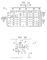
FIG. 3A illustrates one embodiment of a table 60 used to associate bend length 38 of bends 32 with contour adjustment data 26. In particular, for various ranges of bend length 38, such as the ranges defined by bend lengths 38 a-e, table 60 associates the appropriate contour adjustment data 26, such as corner edge data 64 and notch data 66. Corner edge data 64 comprises a corner end length 68 and a corner bend length 70. Notch data 66 comprises a notch end length 72, a notch bend length 74, a notch end depth 76, and a notch bend depth 78.
In one embodiment, contour adjustment data 26 identified in table 60 is optimized through successive adjustments of a transistor channel layout 30 having bends 32 of various lengths 38. For example, given a particular layout 30 a having a bend 32 with a particular length 38, processor 12 adjusts layout 30 a using particular contour adjustment data 26 and generates the output layout data 28 that defines the adjusted layout 30 b. Processor 12 then models a photomask defining a simulated transistor channel according to the output layout data 28. Processor 12 measures various dimensions (e.g., lengths 52) and/or performance parameters (e.g., clock speed) associated with the simulated transistor channel. If the measured dimensions and/or performance characteristics do not meet particular transistor parameters, then processor 12 again adjusts layout 30 using modified contour adjustment data 26. Processor 12 repeats this process of adjusting layouts 30 and simulating transistor channels using output layout data 28 until the simulated transistor channel meets the appropriate transistor parameters. In a particular embodiment, a user of application 22 manually adjusts a layout 30 through successive iterations until the simulated transistor channel meets the appropriate transistor parameters.
The contour adjustment data 26 used to simulate the transistor channel that achieves the transistor parameters are then captured and categorized in table 60 according to the bend length 38 of the bend 32 in the original input layout 30 a. By repeating this optimization of contour adjustment data 26 for bends 32 of varying bend lengths 38, a table 60 of data 26 is generated. When processor 12 encounters a layout 30 having a bend 32 with a particular bend length 38, processor 12 retrieves the appropriate contour adjustment data 26 from table 60 to generate an adjusted layout 30 b and the appropriate output layout data 28. In this respect, contour adjustment data 26 identified in table 60 represents data that may be collected through iterative modeling and optimization techniques.
FIG. 3B illustrates adjustments made to a layout 30 using contour adjustment data 26. For example, corner end length 68 and corner bend length 70 define a portion of layout 30 that is removed to form a corner edge 90. By varying lengths 68 and 70, the angle of corner edge 90 may be adjusted an appropriate amount. Notch end length 72, notch bend length 74, notch end depth 76, and notch bend depth 78 define a portion of layout 30 that is removed to form a notch 92.
The particular values for contour adjustment data 26 used to form corner edge 90 and notch 92 are determined according to bend length 38 as defined by the associations illustrated in table 60 of FIG. 3A. By strategically removing portions of layout 30 using contour adjustment data 26, a particular input transistor channel layout 30 a may be adjusted to form an adjusted transistor channel layout 30 b, as illustrated in FIG. 4. The adjusted transistor channel layout 30 b may then be used to fabricate a transistor channel that meets particular dimension and/or performance parameters, as described in greater detail with reference to FIG. 5.
FIG. 4 illustrates a transistor channel layout 30 b adjusted by processor 12 according to the appropriate contour adjustment data 26. Bend 32 of layout 30 b includes inner corners and outer corners. In one embodiment, a portion of the outer corners is removed to form corner edges 90. By strategically varying the corner end length 68 and the corner bend length 70, the corner edge 90 may be formed at a particular angle.
In another embodiment, a portion of the inner corners is removed to form notches 92. By strategically varying notch end length 72, notch bend length 74, notch end depth 76, and/or notch bend depth 78, notches 92 may be specifically formed to have a particular size, shape, and/or dimension. In a particular embodiment, notch 92 is asymmetrically formed by providing different values for notch end length 72 and notch bend length 74 and/or notch end depth 76 and notch bend depth 78.
FIG. 5 illustrates one embodiment of a transistor channel 50 fabricated on a silicon substrate using a photomask derived from the transistor channel layout 30 b illustrated in FIG. 4. Transistor channel 50 comprises a bend 32 between a first end 34 and a second end 36. In addition, channel 50 comprises channel lengths 52 a-c measured at various positions along the width of channel 50. One advantage to fabricating a transistor channel 50 using an adjusted transistor channel layout 30 b is that channel length 52 is uniform over the width of the channel from first end 32 to second end 34. In particular, channel length 52 a is substantially the same as channel length 52 b and channel length 52 c. This results in a high transistor packing density while maintaining transistor performance and speed.
FIG. 6 is a flow chart of an exemplary method for processing a transistor channel layout 30. The method begins at step 100 where processor 12 launches application 22. Processor 12 receives input layout data 24 defining an input transistor channel layout 30 a, at step 102. Layout 30 a comprises one or more bends 32 between a first end 34 and a second end 36. Processor 12 determines the bend length 38 of each bend 32, at step 104. For each bend 32 of a layout 30 a, processor 12 receives contour adjustment data 26 at step 106. In one embodiment, processor 12 retrieves contour adjustment data 26 from table 60 stored in memory 18, according to the appropriate bend length 38 determined at step 104. In this embodiment, contour adjustment data 26 has been determined to provide an adjusted output layout 30 b that yields a transistor channel 50 which meets the appropriate dimension and/or performance parameters of the transistor, as described above with respect to FIG. 3A.
In another embodiment, processor 12 receives contour adjustment data 26 from a user of application 22. In this embodiment, processor 12 adjusts layout 30 in response to user input through successive iterations until the simulated transistor channel meets the appropriate dimension and/or performance parameters, as described in greater detail with reference to steps 108-112. Processor 12 adjusts transistor channel layout 30 according to the contour adjustment data 26 received at step 106, at step 108. In particular, processor 12 may form corner edges 90 and/or notches 92 in bends 32 of a particular layout 30 using corner edge data 64 and/or notch data 66. Processor 12 generates output layout data 28 defining the adjusted transistor channel layout 30 b generated at step 108, at step 110. Execution proceeds to step 112 where processor 12 models a photomask defining a simulated transistor channel according to the output layout data 28 generated at step 110.
Although the present invention has been described with several embodiments, a myriad of changes, variations, alterations, transformations and modifications may be suggested to one skilled in the art, and it is intended that the present invention encompasses such changes, variations, alterations, transformations, and modifications as fall within the spirit and scope of the appended claims.
Claims (15)
1. A system for processing a transistor channel layout, comprising:
a memory operable to store:
input layout data defining a transistor channel layout having a bend between a first end and a second end; and
contour adjustment data; and
a processor coupled to the memory and operable to:
adjust the bend of the transistor channel layout according to the contour adjustment data; and
generate output layout data defining the adjusted transistor channel layout.
2. The system of claim 1 , wherein the bend of the transistor channel layout comprises a bend length.
3. The system of claim 2 , wherein the contour adjustment data comprise first corner length data and second corner length data selected based upon the bend length.
4. The system of claim 3 , wherein the processor is operable to adjust the bend of the transistor channel layout according to the first corner length data and the second corner length data.
5. The system of claim 2 , wherein the contour adjustment data comprise notch length data and notch depth data selected based upon the bend length.
6. The system of claim 5 , wherein the processor is operable to adjust the bend of the transistor channel layout according to the notch length data and the notch depth data.
7. The system of claim 1 , wherein the processor is further operable to model a photomask defining a simulated transistor channel according to the output layout data, wherein the length of the simulated transistor channel at the bend is substantially equal to the length of the simulated transistor channel at the first end and the length of the simulated transistor channel at the second end.
8. A method for processing a transistor channel layout, comprising:
receiving input layout data defining a transistor channel layout having a bend between a first end and a second end;
receiving contour adjustment data;
adjusting the bend of the transistor channel layout according to the contour adjustment data; and
generating output layout data defining the adjusted transistor channel layout.
9. The method of claim 8 , further comprising receiving a bend length associated with the bend of the transistor channel layout.
10. The method of claim 9 , further comprising selecting particular contour adjustment data based upon the bend length.
11. The method of claim 10 , wherein the particular contour adjustment data comprise first corner length data and second corner length data.
12. The method of claim 11 , further comprising adjusting the bend of the transistor channel layout according to the first corner length data and the second corner length data.
13. The method of claim 10 , wherein the particular contour adjustment data comprise notch length data and notch depth data.
14. The method of claim 13 , further comprising adjusting the bend of the transistor channel layout according to the notch length data and the notch depth data.
15. The method of claim 8 , further comprising modeling a photomask according to the output layout data, the photomask defining a simulated transistor channel having a bend between a first end and a second end, wherein the length of the simulated transistor channel at the bend is substantially equal to the length of the simulated transistor channel at the first end and the length of the simulated transistor channel at the second end.
Priority Applications (1)
| Application Number | Priority Date | Filing Date | Title |
|---|---|---|---|
| US09/932,310 US6668366B2 (en) | 2000-08-18 | 2001-08-17 | System and method for processing a transistor channel layout |
Applications Claiming Priority (2)
| Application Number | Priority Date | Filing Date | Title |
|---|---|---|---|
| US22636900P | 2000-08-18 | 2000-08-18 | |
| US09/932,310 US6668366B2 (en) | 2000-08-18 | 2001-08-17 | System and method for processing a transistor channel layout |
Publications (2)
| Publication Number | Publication Date |
|---|---|
| US20020023254A1 US20020023254A1 (en) | 2002-02-21 |
| US6668366B2 true US6668366B2 (en) | 2003-12-23 |
Family
ID=26920465
Family Applications (1)
| Application Number | Title | Priority Date | Filing Date |
|---|---|---|---|
| US09/932,310 Expired - Lifetime US6668366B2 (en) | 2000-08-18 | 2001-08-17 | System and method for processing a transistor channel layout |
Country Status (1)
| Country | Link |
|---|---|
| US (1) | US6668366B2 (en) |
Cited By (2)
| Publication number | Priority date | Publication date | Assignee | Title |
|---|---|---|---|---|
| US8813017B2 (en) * | 2006-02-17 | 2014-08-19 | Mentor Graphics Corporation | Gate modeling for semiconductor fabrication process effects |
| US10216890B2 (en) | 2004-04-21 | 2019-02-26 | Iym Technologies Llc | Integrated circuits having in-situ constraints |
Families Citing this family (1)
| Publication number | Priority date | Publication date | Assignee | Title |
|---|---|---|---|---|
| US7389483B2 (en) * | 2005-06-22 | 2008-06-17 | Faraday Technology Corp. | Method for auto enlarging bend portion width and computer readable recording medium for storing program thereof |
Citations (6)
| Publication number | Priority date | Publication date | Assignee | Title |
|---|---|---|---|---|
| US5157618A (en) * | 1988-03-10 | 1992-10-20 | Cirrus Logic, Inc. | Programmable tiles |
| US5493509A (en) * | 1992-09-22 | 1996-02-20 | Kabushiki Kaisha Toshiba | Method of and apparatus for generating mask layouts |
| US5526303A (en) * | 1992-11-30 | 1996-06-11 | Fujitsu Limited | Semiconductor memory device having SRAM cells |
| US5610832A (en) * | 1994-11-22 | 1997-03-11 | Mentor Graphics Corporation | Integrated circuit design apparatus with multiple connection modes |
| US5701255A (en) * | 1994-09-14 | 1997-12-23 | Matsushita Electric Industrial Co., Ltd. | Cell generation method and cell generation system |
| US6005296A (en) * | 1997-05-30 | 1999-12-21 | Stmicroelectronics, Inc. | Layout for SRAM structure |
-
2001
- 2001-08-17 US US09/932,310 patent/US6668366B2/en not_active Expired - Lifetime
Patent Citations (6)
| Publication number | Priority date | Publication date | Assignee | Title |
|---|---|---|---|---|
| US5157618A (en) * | 1988-03-10 | 1992-10-20 | Cirrus Logic, Inc. | Programmable tiles |
| US5493509A (en) * | 1992-09-22 | 1996-02-20 | Kabushiki Kaisha Toshiba | Method of and apparatus for generating mask layouts |
| US5526303A (en) * | 1992-11-30 | 1996-06-11 | Fujitsu Limited | Semiconductor memory device having SRAM cells |
| US5701255A (en) * | 1994-09-14 | 1997-12-23 | Matsushita Electric Industrial Co., Ltd. | Cell generation method and cell generation system |
| US5610832A (en) * | 1994-11-22 | 1997-03-11 | Mentor Graphics Corporation | Integrated circuit design apparatus with multiple connection modes |
| US6005296A (en) * | 1997-05-30 | 1999-12-21 | Stmicroelectronics, Inc. | Layout for SRAM structure |
Cited By (4)
| Publication number | Priority date | Publication date | Assignee | Title |
|---|---|---|---|---|
| US10216890B2 (en) | 2004-04-21 | 2019-02-26 | Iym Technologies Llc | Integrated circuits having in-situ constraints |
| US10846454B2 (en) | 2004-04-21 | 2020-11-24 | Iym Technologies Llc | Integrated circuits having in-situ constraints |
| US10860773B2 (en) | 2004-04-21 | 2020-12-08 | Iym Technologies Llc | Integrated circuits having in-situ constraints |
| US8813017B2 (en) * | 2006-02-17 | 2014-08-19 | Mentor Graphics Corporation | Gate modeling for semiconductor fabrication process effects |
Also Published As
| Publication number | Publication date |
|---|---|
| US20020023254A1 (en) | 2002-02-21 |
Similar Documents
| Publication | Publication Date | Title |
|---|---|---|
| US9852251B2 (en) | Manipulating parameterized cell devices in a custom layout design | |
| US8418087B2 (en) | Analyzing multiple induced systematic and statistical layout dependent effects on circuit performance | |
| US10248751B2 (en) | Alternative hierarchical views of a circuit design | |
| US8635580B2 (en) | Preconditioning for EDA cell library | |
| KR101143191B1 (en) | Aligned behavior in templated lists | |
| US7467077B2 (en) | Mesh model creating method, simulation apparatus and computer-readable storage medium | |
| JPH11191116A (en) | System design and evaluation cad system and program storage medium therefor | |
| WO2001042964A2 (en) | Method and apparatus for structure prediction based on model curvature | |
| Abboud et al. | Mask data processing in the era of multibeam writers | |
| US6920620B2 (en) | Method and system for creating test component layouts | |
| US8024685B2 (en) | Delay analysis support apparatus, delay analysis support method and computer product | |
| US20100131249A1 (en) | Method and apparatus for supporting verification of leakage current distribution | |
| CN102446237A (en) | Design method for non-shrinkable IP integration | |
| US6668366B2 (en) | System and method for processing a transistor channel layout | |
| US20030027064A1 (en) | Exposure method for correcting dimension variation in electron beam lithography, and recording medium for recording the same | |
| JP2002072441A (en) | Layout pattern data correction aperture and method of manufacturing semiconductor device using the same as well as medium recorded with layout pattern data correction program | |
| US9195791B2 (en) | Custom module generation | |
| US7406675B2 (en) | Method and system for improving aerial image simulation speeds | |
| US7331026B2 (en) | Method and system for generating an initial layout of an integrated circuit | |
| Shendre et al. | You don’t need 1nm contours for curvilinear shapes: pixel-based computing is the answer | |
| US20060136189A1 (en) | Method and apparatus for integrating a simulation log into a verification environment | |
| US8849440B2 (en) | Manufacturing control based on a final design structure incorporating both layout and client-specific manufacturing information | |
| US20030052881A1 (en) | Graphical value display program, graphical value display method and recording medium | |
| US20110078649A1 (en) | Wafer layout assisting method and system | |
| JP4048752B2 (en) | Pattern data correction method, pattern data correction apparatus and program thereof |
Legal Events
| Date | Code | Title | Description |
|---|---|---|---|
| AS | Assignment |
Owner name: TEXAS INSTRUMENTS INCORPORATED, TEXAS Free format text: ASSIGNMENT OF ASSIGNORS INTEREST;ASSIGNORS:LIAO, HONGMEI;JOHANNESMEYER, SCOTT A.;REEL/FRAME:012105/0714;SIGNING DATES FROM 20000707 TO 20000808 |
|
| STCF | Information on status: patent grant |
Free format text: PATENTED CASE |
|
| FPAY | Fee payment |
Year of fee payment: 4 |
|
| FPAY | Fee payment |
Year of fee payment: 8 |
|
| FPAY | Fee payment |
Year of fee payment: 12 |