US6670694B2 - Semiconductor device - Google Patents
Semiconductor device Download PDFInfo
- Publication number
- US6670694B2 US6670694B2 US09/916,506 US91650601A US6670694B2 US 6670694 B2 US6670694 B2 US 6670694B2 US 91650601 A US91650601 A US 91650601A US 6670694 B2 US6670694 B2 US 6670694B2
- Authority
- US
- United States
- Prior art keywords
- surface orientation
- silicon
- insulating film
- film
- gate insulating
- Prior art date
- Legal status (The legal status is an assumption and is not a legal conclusion. Google has not performed a legal analysis and makes no representation as to the accuracy of the status listed.)
- Expired - Fee Related
Links
- 239000004065 semiconductor Substances 0.000 title claims description 32
- XUIMIQQOPSSXEZ-UHFFFAOYSA-N Silicon Chemical compound [Si] XUIMIQQOPSSXEZ-UHFFFAOYSA-N 0.000 claims abstract description 255
- 229910052710 silicon Inorganic materials 0.000 claims abstract description 255
- 239000010703 silicon Substances 0.000 claims abstract description 255
- 239000000758 substrate Substances 0.000 claims abstract description 157
- 230000005669 field effect Effects 0.000 claims description 35
- 239000000203 mixture Substances 0.000 claims description 7
- 239000000463 material Substances 0.000 claims description 5
- 238000000034 method Methods 0.000 description 111
- 239000012535 impurity Substances 0.000 description 45
- 230000003647 oxidation Effects 0.000 description 37
- 238000007254 oxidation reaction Methods 0.000 description 37
- 238000004519 manufacturing process Methods 0.000 description 24
- 238000010438 heat treatment Methods 0.000 description 20
- VYPSYNLAJGMNEJ-UHFFFAOYSA-N Silicium dioxide Chemical compound O=[Si]=O VYPSYNLAJGMNEJ-UHFFFAOYSA-N 0.000 description 17
- 230000000694 effects Effects 0.000 description 17
- 229910052814 silicon oxide Inorganic materials 0.000 description 16
- 238000005530 etching Methods 0.000 description 15
- 229910021420 polycrystalline silicon Inorganic materials 0.000 description 14
- 229920005591 polysilicon Polymers 0.000 description 14
- 229910021332 silicide Inorganic materials 0.000 description 13
- FVBUAEGBCNSCDD-UHFFFAOYSA-N silicide(4-) Chemical compound [Si-4] FVBUAEGBCNSCDD-UHFFFAOYSA-N 0.000 description 13
- 229910052751 metal Inorganic materials 0.000 description 11
- 239000002184 metal Substances 0.000 description 11
- IJGRMHOSHXDMSA-UHFFFAOYSA-N Atomic nitrogen Chemical compound N#N IJGRMHOSHXDMSA-UHFFFAOYSA-N 0.000 description 10
- 239000007789 gas Substances 0.000 description 10
- 229910007258 Si2H4 Inorganic materials 0.000 description 8
- QVGXLLKOCUKJST-UHFFFAOYSA-N atomic oxygen Chemical compound [O] QVGXLLKOCUKJST-UHFFFAOYSA-N 0.000 description 8
- 230000001590 oxidative effect Effects 0.000 description 8
- 239000001301 oxygen Substances 0.000 description 8
- 229910052760 oxygen Inorganic materials 0.000 description 8
- ZOXJGFHDIHLPTG-UHFFFAOYSA-N Boron Chemical compound [B] ZOXJGFHDIHLPTG-UHFFFAOYSA-N 0.000 description 7
- 229910052785 arsenic Inorganic materials 0.000 description 7
- RQNWIZPPADIBDY-UHFFFAOYSA-N arsenic atom Chemical compound [As] RQNWIZPPADIBDY-UHFFFAOYSA-N 0.000 description 7
- 229910052796 boron Inorganic materials 0.000 description 7
- 238000002955 isolation Methods 0.000 description 7
- 239000012299 nitrogen atmosphere Substances 0.000 description 7
- 229910052581 Si3N4 Inorganic materials 0.000 description 6
- 239000003990 capacitor Substances 0.000 description 5
- 229910052681 coesite Inorganic materials 0.000 description 5
- 229910052906 cristobalite Inorganic materials 0.000 description 5
- 229910052757 nitrogen Inorganic materials 0.000 description 5
- 239000000377 silicon dioxide Substances 0.000 description 5
- 229910052682 stishovite Inorganic materials 0.000 description 5
- 229910052905 tridymite Inorganic materials 0.000 description 5
- 230000008901 benefit Effects 0.000 description 4
- 238000010586 diagram Methods 0.000 description 4
- HQVNEWCFYHHQES-UHFFFAOYSA-N silicon nitride Chemical compound N12[Si]34N5[Si]62N3[Si]51N64 HQVNEWCFYHHQES-UHFFFAOYSA-N 0.000 description 4
- -1 SiHCl4 Chemical compound 0.000 description 2
- 229910004298 SiO 2 Inorganic materials 0.000 description 2
- GWEVSGVZZGPLCZ-UHFFFAOYSA-N Titan oxide Chemical compound O=[Ti]=O GWEVSGVZZGPLCZ-UHFFFAOYSA-N 0.000 description 2
- MCMNRKCIXSYSNV-UHFFFAOYSA-N Zirconium dioxide Chemical compound O=[Zr]=O MCMNRKCIXSYSNV-UHFFFAOYSA-N 0.000 description 2
- PNEYBMLMFCGWSK-UHFFFAOYSA-N aluminium oxide Inorganic materials [O-2].[O-2].[O-2].[Al+3].[Al+3] PNEYBMLMFCGWSK-UHFFFAOYSA-N 0.000 description 2
- 238000005229 chemical vapour deposition Methods 0.000 description 2
- 229910052593 corundum Inorganic materials 0.000 description 2
- 238000012986 modification Methods 0.000 description 2
- 230000004048 modification Effects 0.000 description 2
- 229910001845 yogo sapphire Inorganic materials 0.000 description 2
- 229910002244 LaAlO3 Inorganic materials 0.000 description 1
- BPQQTUXANYXVAA-UHFFFAOYSA-N Orthosilicate Chemical compound [O-][Si]([O-])([O-])[O-] BPQQTUXANYXVAA-UHFFFAOYSA-N 0.000 description 1
- 229910007264 Si2H6 Inorganic materials 0.000 description 1
- 229910003910 SiCl4 Inorganic materials 0.000 description 1
- BLRPTPMANUNPDV-UHFFFAOYSA-N Silane Chemical compound [SiH4] BLRPTPMANUNPDV-UHFFFAOYSA-N 0.000 description 1
- 229910002370 SrTiO3 Inorganic materials 0.000 description 1
- ATJFFYVFTNAWJD-UHFFFAOYSA-N Tin Chemical compound [Sn] ATJFFYVFTNAWJD-UHFFFAOYSA-N 0.000 description 1
- 230000015556 catabolic process Effects 0.000 description 1
- 238000003486 chemical etching Methods 0.000 description 1
- 230000000295 complement effect Effects 0.000 description 1
- 239000013078 crystal Substances 0.000 description 1
- PZPGRFITIJYNEJ-UHFFFAOYSA-N disilane Chemical compound [SiH3][SiH3] PZPGRFITIJYNEJ-UHFFFAOYSA-N 0.000 description 1
- 230000002708 enhancing effect Effects 0.000 description 1
- 238000000407 epitaxy Methods 0.000 description 1
- CMIHHWBVHJVIGI-UHFFFAOYSA-N gadolinium(III) oxide Inorganic materials [O-2].[O-2].[O-2].[Gd+3].[Gd+3] CMIHHWBVHJVIGI-UHFFFAOYSA-N 0.000 description 1
- 229910052732 germanium Inorganic materials 0.000 description 1
- GNPVGFCGXDBREM-UHFFFAOYSA-N germanium atom Chemical compound [Ge] GNPVGFCGXDBREM-UHFFFAOYSA-N 0.000 description 1
- CJNBYAVZURUTKZ-UHFFFAOYSA-N hafnium(IV) oxide Inorganic materials O=[Hf]=O CJNBYAVZURUTKZ-UHFFFAOYSA-N 0.000 description 1
- 238000010030 laminating Methods 0.000 description 1
- MRELNEQAGSRDBK-UHFFFAOYSA-N lanthanum oxide Inorganic materials [O-2].[O-2].[O-2].[La+3].[La+3] MRELNEQAGSRDBK-UHFFFAOYSA-N 0.000 description 1
- 239000007791 liquid phase Substances 0.000 description 1
- 238000004518 low pressure chemical vapour deposition Methods 0.000 description 1
- 229910044991 metal oxide Inorganic materials 0.000 description 1
- 150000004706 metal oxides Chemical class 0.000 description 1
- 150000004767 nitrides Chemical class 0.000 description 1
- KTUFCUMIWABKDW-UHFFFAOYSA-N oxo(oxolanthaniooxy)lanthanum Chemical compound O=[La]O[La]=O KTUFCUMIWABKDW-UHFFFAOYSA-N 0.000 description 1
- HYXGAEYDKFCVMU-UHFFFAOYSA-N scandium(III) oxide Inorganic materials O=[Sc]O[Sc]=O HYXGAEYDKFCVMU-UHFFFAOYSA-N 0.000 description 1
- FDNAPBUWERUEDA-UHFFFAOYSA-N silicon tetrachloride Chemical compound Cl[Si](Cl)(Cl)Cl FDNAPBUWERUEDA-UHFFFAOYSA-N 0.000 description 1
- 229910014031 strontium zirconium oxide Inorganic materials 0.000 description 1
- 239000000126 substance Substances 0.000 description 1
- 230000003746 surface roughness Effects 0.000 description 1
- PBCFLUZVCVVTBY-UHFFFAOYSA-N tantalum pentoxide Inorganic materials O=[Ta](=O)O[Ta](=O)=O PBCFLUZVCVVTBY-UHFFFAOYSA-N 0.000 description 1
- 230000036962 time dependent Effects 0.000 description 1
- 238000000038 ultrahigh vacuum chemical vapour deposition Methods 0.000 description 1
- RUDFQVOCFDJEEF-UHFFFAOYSA-N yttrium(III) oxide Inorganic materials [O-2].[O-2].[O-2].[Y+3].[Y+3] RUDFQVOCFDJEEF-UHFFFAOYSA-N 0.000 description 1
Images


Classifications
-
- H—ELECTRICITY
- H01—ELECTRIC ELEMENTS
- H01L—SEMICONDUCTOR DEVICES NOT COVERED BY CLASS H10
- H01L29/00—Semiconductor devices adapted for rectifying, amplifying, oscillating or switching, or capacitors or resistors with at least one potential-jump barrier or surface barrier, e.g. PN junction depletion layer or carrier concentration layer; Details of semiconductor bodies or of electrodes thereof ; Multistep manufacturing processes therefor
- H01L29/66—Types of semiconductor device ; Multistep manufacturing processes therefor
- H01L29/66007—Multistep manufacturing processes
- H01L29/66075—Multistep manufacturing processes of devices having semiconductor bodies comprising group 14 or group 13/15 materials
- H01L29/66227—Multistep manufacturing processes of devices having semiconductor bodies comprising group 14 or group 13/15 materials the devices being controllable only by the electric current supplied or the electric potential applied, to an electrode which does not carry the current to be rectified, amplified or switched, e.g. three-terminal devices
- H01L29/66409—Unipolar field-effect transistors
- H01L29/66477—Unipolar field-effect transistors with an insulated gate, i.e. MISFET
- H01L29/66568—Lateral single gate silicon transistors
- H01L29/66651—Lateral single gate silicon transistors with a single crystalline channel formed on the silicon substrate after insulating device isolation
-
- H—ELECTRICITY
- H01—ELECTRIC ELEMENTS
- H01L—SEMICONDUCTOR DEVICES NOT COVERED BY CLASS H10
- H01L27/00—Devices consisting of a plurality of semiconductor or other solid-state components formed in or on a common substrate
- H01L27/02—Devices consisting of a plurality of semiconductor or other solid-state components formed in or on a common substrate including semiconductor components specially adapted for rectifying, oscillating, amplifying or switching and having at least one potential-jump barrier or surface barrier; including integrated passive circuit elements with at least one potential-jump barrier or surface barrier
- H01L27/04—Devices consisting of a plurality of semiconductor or other solid-state components formed in or on a common substrate including semiconductor components specially adapted for rectifying, oscillating, amplifying or switching and having at least one potential-jump barrier or surface barrier; including integrated passive circuit elements with at least one potential-jump barrier or surface barrier the substrate being a semiconductor body
- H01L27/08—Devices consisting of a plurality of semiconductor or other solid-state components formed in or on a common substrate including semiconductor components specially adapted for rectifying, oscillating, amplifying or switching and having at least one potential-jump barrier or surface barrier; including integrated passive circuit elements with at least one potential-jump barrier or surface barrier the substrate being a semiconductor body including only semiconductor components of a single kind
- H01L27/085—Devices consisting of a plurality of semiconductor or other solid-state components formed in or on a common substrate including semiconductor components specially adapted for rectifying, oscillating, amplifying or switching and having at least one potential-jump barrier or surface barrier; including integrated passive circuit elements with at least one potential-jump barrier or surface barrier the substrate being a semiconductor body including only semiconductor components of a single kind including field-effect components only
- H01L27/088—Devices consisting of a plurality of semiconductor or other solid-state components formed in or on a common substrate including semiconductor components specially adapted for rectifying, oscillating, amplifying or switching and having at least one potential-jump barrier or surface barrier; including integrated passive circuit elements with at least one potential-jump barrier or surface barrier the substrate being a semiconductor body including only semiconductor components of a single kind including field-effect components only the components being field-effect transistors with insulated gate
- H01L27/092—Devices consisting of a plurality of semiconductor or other solid-state components formed in or on a common substrate including semiconductor components specially adapted for rectifying, oscillating, amplifying or switching and having at least one potential-jump barrier or surface barrier; including integrated passive circuit elements with at least one potential-jump barrier or surface barrier the substrate being a semiconductor body including only semiconductor components of a single kind including field-effect components only the components being field-effect transistors with insulated gate complementary MIS field-effect transistors
-
- H—ELECTRICITY
- H01—ELECTRIC ELEMENTS
- H01L—SEMICONDUCTOR DEVICES NOT COVERED BY CLASS H10
- H01L21/00—Processes or apparatus adapted for the manufacture or treatment of semiconductor or solid state devices or of parts thereof
- H01L21/70—Manufacture or treatment of devices consisting of a plurality of solid state components formed in or on a common substrate or of parts thereof; Manufacture of integrated circuit devices or of parts thereof
- H01L21/77—Manufacture or treatment of devices consisting of a plurality of solid state components or integrated circuits formed in, or on, a common substrate
- H01L21/78—Manufacture or treatment of devices consisting of a plurality of solid state components or integrated circuits formed in, or on, a common substrate with subsequent division of the substrate into plural individual devices
- H01L21/82—Manufacture or treatment of devices consisting of a plurality of solid state components or integrated circuits formed in, or on, a common substrate with subsequent division of the substrate into plural individual devices to produce devices, e.g. integrated circuits, each consisting of a plurality of components
- H01L21/822—Manufacture or treatment of devices consisting of a plurality of solid state components or integrated circuits formed in, or on, a common substrate with subsequent division of the substrate into plural individual devices to produce devices, e.g. integrated circuits, each consisting of a plurality of components the substrate being a semiconductor, using silicon technology
- H01L21/8232—Field-effect technology
- H01L21/8234—MIS technology, i.e. integration processes of field effect transistors of the conductor-insulator-semiconductor type
- H01L21/8238—Complementary field-effect transistors, e.g. CMOS
- H01L21/823885—Complementary field-effect transistors, e.g. CMOS with a particular manufacturing method of vertical transistor structures, i.e. with channel vertical to the substrate surface
-
- H—ELECTRICITY
- H01—ELECTRIC ELEMENTS
- H01L—SEMICONDUCTOR DEVICES NOT COVERED BY CLASS H10
- H01L27/00—Devices consisting of a plurality of semiconductor or other solid-state components formed in or on a common substrate
- H01L27/02—Devices consisting of a plurality of semiconductor or other solid-state components formed in or on a common substrate including semiconductor components specially adapted for rectifying, oscillating, amplifying or switching and having at least one potential-jump barrier or surface barrier; including integrated passive circuit elements with at least one potential-jump barrier or surface barrier
- H01L27/04—Devices consisting of a plurality of semiconductor or other solid-state components formed in or on a common substrate including semiconductor components specially adapted for rectifying, oscillating, amplifying or switching and having at least one potential-jump barrier or surface barrier; including integrated passive circuit elements with at least one potential-jump barrier or surface barrier the substrate being a semiconductor body
- H01L27/08—Devices consisting of a plurality of semiconductor or other solid-state components formed in or on a common substrate including semiconductor components specially adapted for rectifying, oscillating, amplifying or switching and having at least one potential-jump barrier or surface barrier; including integrated passive circuit elements with at least one potential-jump barrier or surface barrier the substrate being a semiconductor body including only semiconductor components of a single kind
- H01L27/085—Devices consisting of a plurality of semiconductor or other solid-state components formed in or on a common substrate including semiconductor components specially adapted for rectifying, oscillating, amplifying or switching and having at least one potential-jump barrier or surface barrier; including integrated passive circuit elements with at least one potential-jump barrier or surface barrier the substrate being a semiconductor body including only semiconductor components of a single kind including field-effect components only
- H01L27/088—Devices consisting of a plurality of semiconductor or other solid-state components formed in or on a common substrate including semiconductor components specially adapted for rectifying, oscillating, amplifying or switching and having at least one potential-jump barrier or surface barrier; including integrated passive circuit elements with at least one potential-jump barrier or surface barrier the substrate being a semiconductor body including only semiconductor components of a single kind including field-effect components only the components being field-effect transistors with insulated gate
- H01L27/092—Devices consisting of a plurality of semiconductor or other solid-state components formed in or on a common substrate including semiconductor components specially adapted for rectifying, oscillating, amplifying or switching and having at least one potential-jump barrier or surface barrier; including integrated passive circuit elements with at least one potential-jump barrier or surface barrier the substrate being a semiconductor body including only semiconductor components of a single kind including field-effect components only the components being field-effect transistors with insulated gate complementary MIS field-effect transistors
- H01L27/0922—Combination of complementary transistors having a different structure, e.g. stacked CMOS, high-voltage and low-voltage CMOS
-
- H—ELECTRICITY
- H01—ELECTRIC ELEMENTS
- H01L—SEMICONDUCTOR DEVICES NOT COVERED BY CLASS H10
- H01L29/00—Semiconductor devices adapted for rectifying, amplifying, oscillating or switching, or capacitors or resistors with at least one potential-jump barrier or surface barrier, e.g. PN junction depletion layer or carrier concentration layer; Details of semiconductor bodies or of electrodes thereof ; Multistep manufacturing processes therefor
- H01L29/02—Semiconductor bodies ; Multistep manufacturing processes therefor
- H01L29/04—Semiconductor bodies ; Multistep manufacturing processes therefor characterised by their crystalline structure, e.g. polycrystalline, cubic or particular orientation of crystalline planes
- H01L29/045—Semiconductor bodies ; Multistep manufacturing processes therefor characterised by their crystalline structure, e.g. polycrystalline, cubic or particular orientation of crystalline planes by their particular orientation of crystalline planes
-
- H—ELECTRICITY
- H01—ELECTRIC ELEMENTS
- H01L—SEMICONDUCTOR DEVICES NOT COVERED BY CLASS H10
- H01L29/00—Semiconductor devices adapted for rectifying, amplifying, oscillating or switching, or capacitors or resistors with at least one potential-jump barrier or surface barrier, e.g. PN junction depletion layer or carrier concentration layer; Details of semiconductor bodies or of electrodes thereof ; Multistep manufacturing processes therefor
- H01L29/66—Types of semiconductor device ; Multistep manufacturing processes therefor
- H01L29/68—Types of semiconductor device ; Multistep manufacturing processes therefor controllable by only the electric current supplied, or only the electric potential applied, to an electrode which does not carry the current to be rectified, amplified or switched
- H01L29/76—Unipolar devices, e.g. field effect transistors
- H01L29/772—Field effect transistors
- H01L29/78—Field effect transistors with field effect produced by an insulated gate
- H01L29/7833—Field effect transistors with field effect produced by an insulated gate with lightly doped drain or source extension, e.g. LDD MOSFET's; DDD MOSFET's
- H01L29/7834—Field effect transistors with field effect produced by an insulated gate with lightly doped drain or source extension, e.g. LDD MOSFET's; DDD MOSFET's with a non-planar structure, e.g. the gate or the source or the drain being non-planar
-
- H—ELECTRICITY
- H01—ELECTRIC ELEMENTS
- H01L—SEMICONDUCTOR DEVICES NOT COVERED BY CLASS H10
- H01L2924/00—Indexing scheme for arrangements or methods for connecting or disconnecting semiconductor or solid-state bodies as covered by H01L24/00
- H01L2924/0001—Technical content checked by a classifier
- H01L2924/0002—Not covered by any one of groups H01L24/00, H01L24/00 and H01L2224/00
Definitions
- This invention relates to a semiconductor device and more particularly to a CMOS (Complementary Metal Oxide Semiconductor) device used in an LSI (Large Scale Integrated Circuit) of high performance and low power consumption, for example.
- CMOS Complementary Metal Oxide Semiconductor
- LSI Large Scale Integrated Circuit
- MOSFET field effect transistor
- the transistor with the above structure enhances the driving power and has an excellent sub-threshold characteristic and is effective for lowering a gate leakage current which causes a problem in a fine MOSFET (for example, H. S. Momose, T. Ohguro, E. Morifuji, H. Sugaya, S. Nakamura, T. Yoshitomi, H. Kimijima, T. Morimoto, F. Matsuoka, Y. Katsumata, H. Ishiuchi and H. Iwai, “Improvement of direct-tunneling gate leakage current in ultra-thin gate oxide CMOS with TiN gate electrode using non-doped selective epitaxial Si channel technique”, in IEDM Tech. Dig. pp 819-822, December, 1999. (refer to reference document [3]).
- FIG. 22 A and FIG. 22B show a method for manufacturing a transistor with the above structure by taking a conventional CMOS device as an example.
- an element isolation region 102 is formed in the surface portion of a silicon substrate 101 having a normal (100) surface orientation so as to define element regions (N-type well region 103 a, P-type well region 103 b ).
- a silicon sacrificing oxide film (not shown) with a film thickness of 12 nm is formed on the surfaces of the N-type well region 103 a and P-type well region 103 b, arsenic and boron which are impurities are doped.
- a PMOS channel impurity doped region 104 a and NMOS channel impurity doped region 104 b are formed as channel portions each having a desired threshold voltage.
- a pre-heating process at 940° C. is effected as a pre-process for removing residual oxygen in the surface portion of the silicon substrate 101 .
- silicon epitaxial growth layers (non-doped epitaxial silicon layers) 105 a, 105 b are respectively formed with a film thickness of approx. 30 nm on the PMOS channel impurity doped region 104 a and NMOS channel impurity doped region 104 b by use of Si 2 H 4 Cl 2 gas, for example, at the temperature of 800° C. by the reduced pressure chemical vapor deposition (RP-CVD) method.
- RP-CVD reduced pressure chemical vapor deposition
- the gate oxidation process is effected by a furnace oxidation method.
- oxide films used for respectively forming gate insulating films 106 a, 106 b with the preset film thickness are formed on the silicon epitaxial growth layers 105 a, 105 b.
- the gate oxidation process is effected in a condition of the temperature of 800° C. and the oxidizing time of 60 minutes, an oxide film with a film thickness of 5 nm can be formed.
- the furnace oxidation method is used, the gate insulating films 106 a, 106 b with desired film thickness can be formed by adequately selecting the temperature and time.
- gate electrodes 107 a, 107 b having desired gate length are respectively formed together with the gate oxide films 106 a, 106 b.
- the heat treatment is effected in a nitrogen atmosphere at the temperature of 1000° C. for 20 seconds, for example.
- the impurities in the gate electrodes 107 a, 107 b are activated and shallow source/drain regions 108 a, 108 b are formed on the surface portion of the PMOS channel impurity doped region 104 a and NMOS channel impurity doped region 104 b.
- gate side wall portions 109 a, 109 b and deep source/drain regions 110 a, 110 b are formed.
- a PMOS transistor (P-type MOSFET) and NMOS transistor (N-type MOSFET) respectively having the silicon epitaxial growth layers 105 a, 105 b in the channel portions thereof are completed.
- silicide layers are formed on the surface portions of the source/drain regions 110 a, 110 b and the gate electrodes 107 a, 107 b by the known technique. After thus lowering the resistance of each of the electrode portions, the electrode portions are connected to metal interconnections (not shown) via contact portions (not shown).
- the N-type MOSFET is formed on the substrate of the (100) surface orientation or if the P-type MOSFET is formed on the substrate of a surface orientation such as the (110) surface orientation other than the (100) surface orientation, it is known that excellent mobility can be attained.
- a MOSFET having a channel/gate insulating film interface on the substrate of the (111) surface orientation has a problem that the interface state in the interface between the gate insulating film and the silicon substrate is high and a large number of fixed charges are present in the gate insulating film. That is, the reliability of the transistor is lower than that of a MOSFET having a channel/gate insulating film interface on the substrate of the (100) surface orientation.
- the interface state density of the MOSFET on the substrate of the (111) surface orientation was increased to 2.2 times that of the MOSFET on the substrate of the (100) surface orientation. Further, a variation in the threshold voltage and variations in the transconductance and current driving ability are approximately twice larger.
- a semiconductor device including field effect transistors each of which has a gate electrode formed on a semiconductor substrate with a gate insulating film disposed therebetween, a semiconductor layer opposite to the gate electrode forming a channel forming region, and source and drain regions formed on both sides of the channel forming region, comprises a first field effect transistor which has an epitaxial growth layer in the channel forming region and in which a surface portion of the channel forming region formed in contact with the gate insulating film is formed on the substrate of a silicon surface orientation; and a second field effect transistor which has the channel forming region having no epitaxial growth layer and in which a surface portion of the channel forming region formed in contact with the gate insulating film is formed on the substrate of a silicon surface orientation other than the (100) silicon surface orientation.
- a semiconductor device including field effect transistors each of which has a gate electrode formed on a semiconductor substrate with a gate insulating film disposed therebetween, a semiconductor layer opposite to the gate electrode forming a channel forming region, and source and drain regions formed on both sides of the channel forming region, comprises a first field effect transistor which has a first channel impurity profile and in which a surface portion of the channel forming region formed in contact with the gate insulating film is formed on the substrate of a (100) silicon surface orientation; and a second field effect transistor which has a second channel impurity profile and in which a surface portion of the channel forming region formed in contact with the gate insulating film is formed on the substrate of a silicon surface orientation other than the (100) silicon surface orientation; wherein the first channel impurity profile provides a lower concentration in the surface portion of the channel forming region which is formed in contact with the gate insulating film in comparison with the second channel impurity profile.
- a semiconductor device including a field effect transistor which has a gate electrode formed on a semiconductor substrate with a gate insulating film disposed therebetween, a semiconductor layer opposite to the gate electrode forming a channel forming region, and source and drain regions formed on both sides of the channel forming region, comprise a field effect transistor in which a surface portion of the channel forming region formed in contact with the gate insulating film includes a first region having an epitaxial growth layer and formed on the substrate of a (100) silicon surface orientation and a second region having no epitaxial growth layer and formed on the substrate of a silicon surface orientation other than the (100) silicon surface orientation.
- a semiconductor device including a field effect transistor which has a gate electrode formed on a semiconductor substrate with a gate insulating film disposed therebetween, a semiconductor layer opposite to the gate electrode forming a channel forming region, and source and drain regions formed on both sides of the channel forming region, comprises a first field effect transistor which has an epitaxial growth layer on the source/drain region and in which a surface portion of the source/drain region formed in contact with one of a silicide layer and a metal interconnection layer is formed on the substrate of a (100) silicon surface orientation; and a second field effect transistor which has the source/drain region having no epitaxial growth layer formed thereon and in which a surface portion of the source/drain region formed in contact with one of a silicide layer and a metal interconnection layer is formed on the substrate of a silicon surface orientation other than the (100) silicon surface orientation.
- a semiconductor device including a field effect transistor which has a gate electrode formed on a semiconductor substrate with a gate insulating film disposed therebetween, a semiconductor layer opposite to the gate electrode forming a channel forming region, and source and drain regions formed on both sides of the channel forming region, comprises a field effect transistor in which a surface portion of the source/drain region formed in contact with one of a silicide layer and a metal interconnection layer includes a first region having an epitaxial growth layer and formed on the substrate of a (100) silicon surface orientation and a second region having no epitaxial growth layer and formed on the substrate of a silicon surface orientation other than the (100) silicon surface orientation.
- a semiconductor device including field effect transistors each of which has a gate electrode formed on a semiconductor substrate with a gate insulating film disposed therebetween, a semiconductor layer opposite to the gate electrode forming a channel forming region, and source and drain regions formed on both sides of the channel forming region, comprises a first field effect transistor in which a surface portion of the channel forming region formed in contact with the gate insulating film is formed on the substrate of a (100) silicon surface orientation; and a second field effect transistor in which a surface portion of the channel forming region formed in contact with the gate insulating film is formed on the substrate of a silicon surface orientation other than the (100) silicon surface orientation; wherein the film thickness of the gate insulating film of the second field effect transistor expressed in terms of an equivalent oxide thickness is smaller than the film thickness of the gate insulating film of the first field effect transistor expressed in terms of an equivalent oxide thickness.
- a semiconductor device including field effect transistors each of which has a gate electrode formed on a semiconductor substrate with a gate insulating film disposed therebetween, a semiconductor layer opposite to the gate electrode forming a channel forming region, and source and drain regions formed on both sides of the channel forming region, comprises a first field effect transistor in which a surface portion of the channel forming region formed in contact with the gate insulating film is formed on the substrate of a (100) silicon surface orientation; and a second field effect transistor in which a surface portion of the channel forming region formed in contact with the gate insulating film is formed on the substrate of a silicon surface orientation other than the (100) silicon surface orientation; wherein the gate insulating film of the first field effect transistor is constructed as a stacked film of a first insulating film formed in contact with the channel forming region and a second insulating film formed of a material or composition different from the first insulating film, the gate insulating film of the second field effect transistor is constructed as a stacked
- FIG. 1A to FIG. 1D are cross sectional views for illustrating the steps of a method for manufacturing a CMOS device according to a first embodiment of this invention
- FIG. 2A to FIG. 2D are cross sectional views for illustrating the steps of a method for manufacturing a CMOS device according to a second embodiment of this invention
- FIG. 3A to FIG. 3D are cross sectional views for illustrating the steps of a method for manufacturing a different structure of the CMOS device according to the second embodiment of this invention.
- FIG. 4 is a perspective view for illustrating a method for manufacturing a still different structure of the CMOS device according to the second embodiment of this invention.
- FIG. 5A to FIG. 5D are cross sectional views for illustrating the steps of a method for manufacturing the CMOS device shown in FIG. 4;
- FIG. 6A to FIG. 6D are cross sectional views for illustrating the steps of a method for manufacturing a CMOS device according to a third embodiment of this invention.
- FIG. 7A to FIG. 7C are cross sectional views showing a first example of the structure, for illustrating the steps of a method for manufacturing a CMOS device according to a fourth embodiment of this invention.
- FIG. 8A to FIG. 8C are cross sectional views showing a second example of the structure, for illustrating the steps of a method for manufacturing the CMOS device according to the fourth embodiment of this invention.
- FIG. 9A to FIG. 9C are cross sectional views showing a third example of the structure, for illustrating the steps of a method for manufacturing the CMOS device according to the fourth embodiment of this invention.
- FIG. 10 is a cross sectional view showing a fourth example of the structure, for illustrating a method for manufacturing the CMOS device according to the fourth embodiment of this invention.
- FIG. 11A to FIG. 11C are cross sectional views showing a first example of the structure, for illustrating the steps of a method for manufacturing a CMOS device according to a fifth embodiment of this invention.
- FIG. 12A to FIG. 12C are cross sectional views showing a second example of the structure, for illustrating the steps of a method for manufacturing the CMOS device according to the fifth embodiment of this invention.
- FIG. 13A to FIG. 13C are cross sectional views showing a third example of the structure, for illustrating the steps of a method for manufacturing the CMOS device according to the fifth embodiment of this invention.
- FIG. 14 is a cross sectional view showing a fourth example of the structure, for illustrating a method for manufacturing the CMOS device according to the fifth embodiment of this invention.
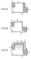
- FIG. 15 A and FIG. 15B are cross sectional views showing examples of gate insulating films of MOSFETs according to a sixth embodiment of this invention.
- FIG. 16 is a characteristic diagram for illustrating a variation in the film thickness of an oxide film in the wafer surface according to this invention.
- FIG. 17 is a characteristic diagram for illustrating variations in the transconductance and threshold voltage of a MOSFET in the wafer surface according to this invention.
- FIG. 18 A and FIG. 18B are characteristic diagrams for illustrating the reliability of a MOS capacitor used as an example according to this invention.
- FIG. 19A to FIG. 19C are cross sectional views for illustrating the steps of a method for manufacturing the CMOS device according to this invention in which a MOSFET having a thick gate oxide film formed on a substrate of a (100) surface orientation and a MOSFET having a thin gate oxide film formed on the substrate of a (111) surface orientation are formed;
- FIG. 20A and 20B are characteristic diagrams for illustrating the relation between the surface orientation and a silicon oxide film in this invention.
- FIG. 21A to FIG. 21D are cross sectional views showing the manufacturing steps of a CMOS device according to this invention in which MOSFETs each having a gate insulating film formed of a stacked film are formed on a substrate of (100) and (111) surface orientations, for example; and
- FIG. 22 A and FIG. 22B are cross sectional views showing the manufacturing steps of a CMOS device, for illustrating the prior art and a problem thereof.
- epitaxial growth on a silicon substrate of (100) surface orientation makes roughness on the silicon surface smaller than on the bulk surface.
- epitaxial growth on a silicon substrate of surface orientation other than the (100) surface orientation increases roughness on the silicon surface.
- Table 1 shows the results of the surface roughness of a silicon bulk (Bulk-Si) and silicon epitaxial growth layer (Epi-Si) evaluated by use of AFM (Atomic Force Microscope).
- Ra least square roughness
- RMS absolute values of deflections from the central surface to the surface on the quantitative surface
- a variation in the roughness of the silicon surface due to the epitaxial growth is extremely strongly influenced by the silicon growth rate in the respective surface orientations. It is predicted that the reason why the results shown in Table 1 are obtained is that the epitaxial growth rate in a direction of (100) surface orientation of silicon is higher than that in a direction of other surface orientations and the epitaxial growth rate in a direction of (111) surface orientation is lower than that in a direction of other surface orientations including the (100) surface orientation.
- the reliability and the characteristic such as a gate leakage current of the transistor are degraded in comparison with the MOSFET on the substrate of the (100) surface orientation since the interface roughness increases.
- the above problem occurs not only in the transistor on the substrate of the (111) surface orientation, but the same problem occurs in a transistor on the substrate of a surface orientation such as (110), (113), (115) on which it is known that the growth rate of silicon is lower than on the (100) surface orientation (for example, refer to C. H. J. Van den Brekel, “Growth rate anisotropy and morphology of autoepitaxial silicon films from SiCl 4 , “J of Crystal Growth, pp. 259-266, 1974, (refer to reference document [4])) or a surface orientation such as (211), (311), (511), (811), (101), (011).
- FIG. 1A to FIG. 1D show a manufacturing method a CMOS device according to a first embodiment of this invention.
- the surface portion of a silicon substrate 11 of (100) surface orientation X is processed by a known technique such as the silicon anisotropic etching technique to expose part of the surface portion having a surface orientation (in this example, (110) surface orientation Y) other than the (100) surface orientation X.
- an element isolation region 12 is formed in the surface portion of the silicon substrate 11 to define element regions (N-type well region 13 a, P-type well region 13 b ).
- the (110) surface orientation Y is formed on the surface portion of the N-type well region 13 a which is a forming region of a second MOSFET (P-type MOSFET) having a second channel impurity profile (refer to FIG. 1 A).
- a silicon sacrificing oxide film (not shown) with a film thickness of 12 nm is formed on the surface portions of the N-type well region 13 a and P-type well region 13 b and then arsenic and boron which are impurities for attaining desired threshold voltages are doped into the channel portions of the N-type well region 13 a and P-type well region 13 b.
- the silicon sacrificing oxide film is removed so as to cover only the N-type well region 13 a with a cover insulating film 21 . That is, the silicon sacrificing oxide film is left behind only on the N-type well region 13 a except the P-type well region 13 b which is the forming region of the first MOSFET (N-type MOSFET) (refer to FIG. 1 B).
- a pre-heating process at 940° C. is effected as a pre-process for removing residual oxygen in the surface portion of the silicon substrate 11 .
- a silicon epitaxial growth layer (non-doped epitaxial silicon layer) 15 having a first channel impurity profile is formed with a film thickness of approx. 30 nm only on the main surface of the P-type well region 13 b which is used as the channel portion of the N-type MOSFET, for example, by use of Si 2 H 4 Cl 2 gas, at the temperature of 800° C. by the RP-CVD method.
- a channel portion of the N-type MOSFET formed on the silicon substrate 11 of the (100) surface orientation X and having an extremely steep impurity concentration gradient is realized.
- cover insulating film (silicon sacrificing oxide film) 21 which covers the N-type well region 13 a is removed.
- the gate oxidation process is effected by a rapid ramp heating (RTO) method.
- RTO rapid ramp heating
- oxide films used for respectively forming gate insulating films 16 a, 16 b with the preset film thickness are formed on the N-type well region 13 a and P-type well region 13 b.
- the gate oxidation process is effected in a condition of the temperature of 800° C. and the oxidizing time of 10 seconds by the RTO method, an oxide film with a film thickness of 1.5 nm can be formed.
- the gate insulating films 16 a, 16 b with desired film thickness can be formed by adequately selecting the temperature and time.
- gate electrodes 17 a, 17 b having desired gate length are respectively formed on the N-type well region 13a and P-type well region 13 b.
- the heat treatment is effected in a nitrogen atmosphere at the temperature of 1000° C. for 20 seconds, for example, in order to diffuse and activate the doped impurity.
- shallow source/drain regions 18 are formed on the surface portion of the P-type well region 13 b.
- gate side wall portions 19 of the gate electrode 17 b and source/drain regions 20 a, 20 b which are deeper than the shallow source/drain regions 18 are formed.
- an NMOS transistor (N-type MOSFET) formed on the silicon substrate 11 of the (100) surface orientation X and having the silicon epitaxial growth layer 15 in the channel portion and a PMOS transistor (P-type MOSFET) formed on the silicon substrate 11 of the (110) surface orientation Y different from the (100) surface orientation X, having no silicon epitaxial growth layer 15 in the channel portion and having the channel portion formed of the N-type well region 13 a are completed (refer to FIG. 1 D).
- silicide layers are formed on the surface portions of the source/drain regions 20 a, 20 b and the gate electrodes 17 a, 17 b. After thus lowering the resistance of each of the electrode portions, the electrode portions are connected to metal interconnections via contact portions.
- MOSFETs with extremely high reliability, small leakage current and excellent noise characteristic can be formed on the same silicon substrate 11 without damaging the advantages of the MOSFETs formed on various surface orientations other than the (100) surface orientation X by using the epitaxial channel structure.
- MOSFETs of the same conductivity type are formed on the silicon substrate of (100) surface orientation and the surface orientation different from the (100) surface orientation (for example, N-type MOSFETs are formed on both of the surface orientations or P-type MOSFETs are formed on both of the surface orientations), MOSFETs with high reliability, small leakage current and excellent noise characteristic can be formed in the same manner.
- a MOSFET having the same conductivity type as and different threshold voltage from a MOSFET formed on the silicon substrate of the surface orientation different from the (100) surface orientation and having no silicon epitaxial growth layer can be formed together with the latter MOSFET on the same silicon substrate by forming a silicon epitaxial growth layer of low concentration only in the channel portion of the MOSFET on the silicon substrate of the (100) surface orientation.
- FIG. 2A to FIG. 2D show a manufacturing method of a CMOS device according to a second embodiment of this invention.
- a case wherein only a surface orientation other than at least a (100) surface orientation, for example, only a (110) surface orientation on a silicon substrate is covered with an insulating film and a silicon epitaxial growth layer is formed on the entire region except the (110) surface orientation is explained.
- the surface portion of a silicon substrate 11 of (100) surface orientation X is processed by a known technique such as the silicon anisotropic etching technique to expose part of the surface portion having a (110) surface orientation Y other than the (100) surface orientation X.
- an element isolation region 12 is formed in the surface portion of the silicon substrate 11 to define element regions (N-type well region 13 a , P-type well region 13 b ).
- the (110) surface orientation Y is formed on the surface portion of the N-type well region 13 a which is a forming region of a second MOSFET (P-type MOSFET) having a second channel impurity profile (refer to FIG. 2 A).
- a silicon sacrificing oxide film (not shown) with a film thickness of 12 nm is formed on the surface portions of the N-type well region 13 a and P-type well region 13 b and then arsenic and boron which are impurities for attaining desired threshold voltages are doped into the channel portions of the N-type well region 13 a and P-type well region 13 b.
- part of the silicon sacrificing oxide film is removed so as to cover the channel forming region of the N-type well region 13 a which lies on the (110) surface orientation Y with a cover insulating film 21 . That is, the silicon sacrificing oxide film is left behind only on a portion of the (110) surface orientation Y except the P-type well region 13 b which is the forming region of the first MOSFET (N-type MOSFET) and a portion of the (100) surface orientation X on the N-type well region 13 a (refer to FIG. 2 B).
- a pre-heating process at 940° C. is effected as a pre-process for removing residual oxygen in the surface portion of the silicon substrate 11 .
- a silicon epitaxial growth layer (non-doped epitaxial silicon layer) 15 having a first channel impurity profile is formed with a film thickness of approx. 30 nm on the portion of (100) surface orientation X containing at least the main surface of the P-type well region 13 b which is used as the channel portion of the N-type MOSFET, for example, by use of Si 2 H 4 Cl 2 gas at the temperature of 800° C. by the RP-CVD method (refer to FIG. 2 C).
- cover insulating film (silicon sacrificing oxide film) 21 which covers the portion of (110) surface orientation Y is removed.
- the gate oxidation process is effected by the RTO method.
- oxide films used for respectively forming gate insulating films 16 a , 16 b with the preset film thickness are formed on the N-type well region 13 a and P-type well region 13 b .
- the gate oxidation process is effected in a condition of the temperature of 800° C. and the oxidizing time of 10 seconds by the RTO method, an oxide film with a film thickness of 1.5 nm can be formed.
- the gate insulating films 16 a , 16 b with desired film thickness can be formed by adequately selecting the temperature and time.
- gate electrodes 17 a , 17 b having desired gate length are respectively formed on the N-type well region 13 a and P-type well region 13 b.
- the heat treatment is effected in a nitrogen atmosphere at the temperature of 1000° C. for approx. 20 seconds, for example.
- shallow source/drain regions 18 are formed on the surface portion of the P-type well region 13 b.
- gate side wall portions 19 of the gate electrode 17 b and source/drain regions 20 a , 20 b which are deeper than the shallow source/drain regions 18 are formed.
- an NMOS transistor (N-type MOSFET) formed on the silicon substrate 11 of the (100) surface orientation X and having the silicon epitaxial growth layer 15 in the channel portion and a PMOS transistor (P-type MOSFET) formed on the silicon substrate of the (110) surface orientation Y different from the (100) surface orientation X, having no silicon epitaxial growth layer 15 in the channel portion and having the channel portion formed of the N-type well region 13 a are completed (refer to FIG. 2 D).
- silicide layers are formed on the surface portions of the source/drain regions 20 a, 20 b and the gate electrodes 17 a , 17 b . After thus lowering the resistance of each of the electrode portions, the electrode portions are connected to metal interconnections via contact portions.
- the silicon epitaxial growth layer 15 is formed on the portion of (100) surface orientation X except the (110) surface orientation Y, the same effect as that obtained in the CMOS device of the first embodiment can be expected.
- the silicon epitaxial growth layer 15 is formed only on the silicon substrate of the (100) surface orientation X and an increase in the roughness on the silicide/silicon interface is suppressed in the source/drain regions 20 a of the MOSFET having the channel portion on the (110) surface orientation Y, an increase in the source/drain junction leak current can be prevented.
- the same effect can be attained by covering a source/drain region 20 a -1 on, for example, a (111) surface orientation Z other than the (100) surface orientation X with the cover insulating film 21 after the gate electrodes 17 a , 17 b are formed and selectively forming silicon epitaxial growth layers 15 on the source/drain regions 20 b of a first MOSFET on the silicon substrate of the (100) surface orientation X and a source/drain region 20 a -2 among the source/drain regions 20 a -1 , 20 a -2 of a second MOSFET having a channel portion on the (111) surface orientation Z which has an exposed surface portion of (100) surface orientation X (so-called elevate source/drain structure).
- FIG. 4 and FIG. 5A to FIG. 5D show examples in which at least a (100) surface orientation X and a surface orientation other than the (100) surface orientation X, for example, a (110) surface orientation Y are exposed to the surface portion of the silicon substrate 11 and a silicon epitaxial growth layer 15 is formed on the entire region except the region of (110) surface orientation Y.
- FIG. 4 is a perspective view of the silicon substrate 11 and FIG. 5A to FIG. 5D are cross sectional views showing the portions of (100) surface orientation X and (110) surface orientation Y.
- the surface portion of the silicon substrate 11 of (100) surface orientation is processed by a known technique such as the silicon anisotropic etching technique to expose part of the surface portion having the (100) surface orientation X and (110) surface orientation Y other than the (100) surface orientation X.
- a known technique such as the silicon anisotropic etching technique to expose part of the surface portion having the (100) surface orientation X and (110) surface orientation Y other than the (100) surface orientation X.
- the (100) surface orientation X and (110) surface orientation Y both make an angle of 90° with respect to the silicon substrate 11 and an angle of 45° (or 135°) is made between the (100) surface orientation X and (110) surface orientation Y.
- an element isolation region 12 is formed in the surface portion of the silicon substrate 11 to define element regions (N-type well region 13 a , P-type well region 13 b ).
- the (100) surface orientation X is formed on the surface portion of the P-type well region 13 b which is a forming region of a first MOSFET (N-type MOSFET) having a first channel impurity profile.
- the (110) surface orientation Y is formed on the surface portion of the N-type well region 13 a which is a forming region of a second MOSFET (P-type MOSFET) having a second channel impurity profile
- a silicon sacrificing oxide film (not shown) with a film thickness of 12 nm is formed on the surface portions of the N-type well region 13 a and P-type well region 13 b and then arsenic and boron which are impurities for attaining desired threshold voltages are doped into the channel portions of the N-type well region 13 a and P-type well region 13 b.
- part of the silicon sacrificing oxide film is removed so as to cover the channel forming region of the N-type well region 13 a which lies on the (110) surface orientation with a cover insulating film 21 . That is, the silicon sacrificing oxide film is left behind only on the (110) surface orientation Y.
- a pre-heating process at 940° C. is effected as a pre-process for removing residual oxygen in the surface portion of the silicon substrate 11 .
- a silicon epitaxial growth layer (non-doped epitaxial silicon layer) 15 having the first channel impurity profile is formed with a film thickness of approx. 30 nm on the silicon substrate of the (100) surface orientation X containing at least the main surface of the P-type well region 13 b which is used as the channel portion of the N-type MOSFET, for example, by use of Si 2 H 4 Cl 2 gas at the temperature of 800° C. by the RP-CVD method.
- cover insulating film (silicon sacrificing oxide film) 21 which covers the on the silicon substrate of the (110) surface orientation Y is removed.
- the gate oxidation process is effected by the RTO method.
- oxide films used for respectively forming gate insulating films 16 a , 16 b with the preset film thickness are formed on the N-type well region 13 a and P-type well region 13 b .
- the gate oxidation process is effected in a condition of the temperature of 800° C. and the oxidizing time of 10 seconds by the RTO method, an oxide film with a film thickness of 1.5 nm can be formed.
- the gate insulating films 16 a , 16 b with desired film thickness can be formed by adequately selecting the temperature and time.
- gate electrodes 17 a , 17 b having desired gate length are respectively formed on the N-type well region 13 a and P-type well region 13 b.
- the present embodiment relates to the gate electrode 17 a of the MOSFET on the silicon substrate 11 of the (110) surface orientation Y and the gate electrode 17 b of the MOSFET on the silicon substrate 11 of the (100) surface orientation X and both of them constitute vertical MOSFET structures in which the gate length directions make 90° with respect to the substrate surface of the silicon substrate 11 of (100) surface orientation. Therefore, the gate electrodes 17 a , 17 b can be formed in the same process, the manufacturing process can be more simplified, consistency of the process is excellent and the process becomes suitable for miniaturization.
- the heat treatment is effected in a nitrogen atmosphere at the temperature of 1000° C. for approx. 20 seconds, for example.
- source/drain regions 20 a , 20 b are respectively formed on the surface portions of the N-type well region 13 a and P-type well region 13 b .
- an N-type MOSFET formed on the silicon substrate of the (100) surface orientation X and having the silicon epitaxial growth layer 15 in the channel portion and a P-type MOSFET formed on the silicon substrate of the (110) surface orientation Y different from the (100) surface orientation, having no silicon epitaxial growth layer 15 in the channel portion and having the channel portion formed of the N-type well region 13 a are completed.
- silicide layers are formed on the surface portions of the source/drain regions 20 a, 20 b and the gate electrodes 17 a , 17 b. After thus lowering the resistance of each of the electrode portions, the electrode portions are connected to metal interconnections via contact portions.
- the channel portion of the N-type MOSFET is formed on the silicon substrate of the (100) surface orientation X and the channel portion of the P-type MOSFET is formed on the silicon substrate of the surface orientation different from the (100) surface orientation is explained.
- excellent mobility can be attained in both of the N-type MOSFET and P-type MOSFET and a CMOS device with high reliability, small leakage current and excellent noise characteristic can be formed.
- MOSFETs of the same conductivity type are formed on the silicon substrate of the (100) surface orientation and the surface orientation different from the (100) surface orientation (for example, N-type MOSFETs are formed on the silicon substrate on both of the surface orientations or P-type MOSFETs are formed on the silicon substrate on both of the surface orientations), MOSFETs with high reliability, small leakage current and excellent noise characteristic can be formed in the same manner.
- a MOSFET having the same conductivity type as and different threshold voltage from a MOSFET formed on the silicon substrate of the surface orientation different from the (100) surface orientation and having no silicon epitaxial growth layer can be formed together with the latter MOSFET on the same silicon substrate by forming a silicon epitaxial growth layer of low concentration only in the channel portion of the MOSFET on the silicon substrate of the (100) surface orientation.
- FIG. 6A to FIG. 6D show a manufacturing method of a CMOS device according to a third embodiment of this invention.
- a P-type MOSFET is formed on a substrate of a surface orientation other than at least a (100) surface orientation, for example, on a (111) surface orientation on a silicon substrate is formed is explained.
- the surface portion of a silicon substrate 11 of (100) surface orientation X is processed by a known technique such as the chemical liquid phase etching technique to form a V-shaped groove in part of the surface portion thereof and expose a (111) surface orientation Z other than the (100) surface orientation X.
- an element isolation region 12 is formed in the surface portion of the silicon substrate 11 to define element regions (N-type well region 13 a , P-type well region 13 b ).
- the (111) surface orientation Z is formed on the surface portion of the N-type well region 13 a which is a forming region of a second MOSFET (P-type MOSFET) having a second channel impurity profile (refer to FIG. 6 A).
- a silicon sacrificing oxide film (not shown) with a film thickness of 12 nm is formed on the surface portions of the N-type well region 13 a and P-type well region 13 b and then arsenic and boron which are impurities for attaining desired threshold voltages are doped into the channel portions of the N-type well region 13 a and P-type well region 13 b.
- part of the silicon sacrificing oxide film is removed so as to cover only the N-type well region 13 a (or a portion of the N-type well region 13 a which lies on at least the (111) surface orientation Z) with a cover insulating film 21 . That is, the silicon sacrificing oxide film is left behind only on the N-type well region 13 a (or a portion of the N-type well region 13 a which lies on the (111) surface orientation Z except the (100) surface orientation X) except the P-type well region 13 b which is the forming region of the first MOSFET (N-type MOSFET) (refer to FIG. 6 B).
- a pre-heating process at 940° C. is effected as a pre-process for removing residual oxygen in the surface portion of the silicon substrate 11 .
- a silicon epitaxial growth layer (non-doped epitaxial silicon layer) 15 having a first channel impurity profile is formed with a film thickness of approx. 30 nm on the (100) surface orientation X of the P-type well region 13 b which is used at least as the channel portion of the N-type MOSFET, for example, by use of Si 2 H 4 Cl 2 gas at the temperature of 800° C. by the RP-CVD method (refer to FIG. 6 C).
- cover insulating film (silicon sacrificing oxide film) 21 which covers at least the (111) surface orientation Z is removed.
- the gate oxidation process is effected by the RTO method.
- oxide films used for respectively forming gate insulating films 16 a , 16 b with the preset film thickness are formed on the N-type well region 13 a and P-type well region 13 b .
- the gate oxidation process is effected in a condition of the temperature of 800° C. and the oxidizing time of 10 seconds by the RTO method, an oxide film with a film thickness of 1.5 nm can be formed.
- the gate insulating films 16 a , 16 b with desired film thickness can be formed by adequately selecting the temperature and time.
- gate electrodes 17 a , 17 b having desired gate length are respectively formed on the N-type well region 13 a and P-type well region 13 b.
- the heat treatment is effected in a nitrogen atmosphere at the temperature of 1000° C. for approx. 20 seconds, for example.
- shallow source/drain regions 18 are formed on the surface portion of the P-type well region 13 b.
- gate side wall portions 19 of the gate electrode 17 b and source/drain regions 20 a , 20 b which are deeper than the shallow source/drain regions 18 are formed.
- an NMOS transistor (N-type MOSFET) formed on the silicon substrate of the (100) surface orientation X and having the silicon epitaxial growth layer 15 in the channel portion and a PMOS transistor (P-type MOSFET) formed on the silicon substrate of the (111) surface orientation Z different from the (100) surface orientation, having no silicon epitaxial growth layer 15 in the channel portion and having the channel portion formed of the N-type well region 13 a are completed (refer to FIG. 6 D).
- silicide layers are formed on the surface portions of the source/drain regions 20 a, 20 b and the gate electrodes 17 a , 17 b. After lowering the resistance of each of the electrodes, the electrodes are connected to metal interconnections via contact portions.
- the channel portion of the N-type MOSFET is formed on the silicon substrate (100) surface orientation X and the channel portion of the P-type MOSFET is formed on the silicon substrate of the surface orientation different from the (100) surface orientation is explained.
- excellent mobility can be attained in both of the N-type MOSFET and P-type MOSFET and a CMOS device with high reliability, small leakage current and excellent noise characteristic can be formed.
- MOSFETs of the same conductivity type are formed on the substrate of the (100) surface orientation and the surface orientation different from the (100) surface orientation (for example, N-type MOSFETs are formed on the silicon substrate on the silicon substrate on both of the surface orientations or P-type MOSFETs are formed on the silicon substrate on the silicon substrate on both of the surface orientations), MOSFETs with high reliability, small leakage current and excellent noise characteristic can be formed in the same manner.
- a MOSFET having the same conductivity type as and different threshold voltage from a MOSFET formed on the silicon substrate of the surface orientation different from the (100) surface orientation and having no silicon epitaxial growth layer can be formed together with the latter MOSFET on the same silicon substrate by forming a silicon epitaxial growth layer of low concentration only in the channel portion of the MOSFET on the silicon substrate of the (100) surface orientation.
- FIG. 7A to FIG. 7C show a manufacturing method of a CMOS device according to a fourth embodiment of this invention.
- the channel portion of a MOSFET is so formed as to have at least a (100) surface orientation and a surface orientation other than the (100) surface orientation, for example, a (110) surface orientation on a silicon substrate in the cross section in the channel width direction is explained.
- the surface portion of a silicon substrate 11 of (100) surface orientation X is processed by a known technique such as the silicon anisotropic etching technique to expose part of the surface portion having a surface orientation such as a (110) surface orientation Y other than the (100) surface orientation.
- a known technique such as the silicon anisotropic etching technique to expose part of the surface portion having a surface orientation such as a (110) surface orientation Y other than the (100) surface orientation.
- an element isolation region 12 is formed in the surface portion of the silicon substrate 11 to define regions in which the channel portion of a transistor is formed.
- the (110) surface orientation Y is exposed in addition to the (100) surface orientation in the cross section in the channel width direction in order to enhance the current driving ability for each unit area.
- a silicon sacrificing oxide film (not shown) with a film thickness of 12 nm is formed on the surface portion of the silicon substrate 11 and then boron or arsenic which is impurity for attaining desired threshold voltage is doped into the channel portion in the case of an N-type MOSFET or a P-type MOSFET, respectively.
- part of the silicon sacrificing oxide film is removed so as to cover only the portion of (110) surface orientation Y of the silicon substrate 11 with a cover insulating film 21 . That is, the silicon sacrificing oxide film is left behind only on the portion of (110) surface orientation Y other than the (100) surface orientation X.
- a pre-heating process at 940° C. is effected as a pre-process for removing residual oxygen in the surface portion of the silicon substrate 11 .
- a silicon epitaxial growth layer (non-doped epitaxial silicon layer) 15 is formed with a film thickness of approx. 30 nm on the silicon substrate of the (100) surface orientation X, for example, by use of Si 2 H 4 Cl 2 gas, at the temperature of 800° C. by the RP-CVD method.
- cover insulating film (silicon sacrificing oxide film) 21 which covers on the silicon substrate of the (110) surface orientation Y is removed.
- the gate oxidation process is effected by the RTO method.
- an oxide film used for forming a gate insulating film 16 with the preset film thickness is formed.
- the gate oxidation process is effected in a condition of the temperature of 800° C. and the oxidizing time of 10 seconds by the RTO method, an oxide film with a film thickness of 1.5 nm can be formed.
- the gate insulating film 16 with desired film thickness can be formed by adequately selecting the temperature and time.
- a gate electrode 17 having desired gate width is formed.
- the heat treatment is effected in a nitrogen atmosphere at the temperature of 1000° C. for 20 seconds, for example, so as to diffuse and activate the doped impurity.
- silicide layers are formed on the surface portions of the source/drain regions and the gate electrode 17 . After thus lowering the resistance of each of the electrode portions, the electrode portions are connected to metal interconnections via contact portions.
- a portion indicated by a range A becomes almost equal to the channel width in the cross section in the channel width direction.
- the channel width can be made larger than the gate width as viewed from above the wafer. Therefore, the driving power can be further enhanced and the structure is made suitable for miniaturization.
- the channel portion of the transistor is formed to contain the silicon surface portion on the (110) surface orientation Y.
- the channel portion (channel width A) of the transistor can be formed to contain the silicon surface portion on the (111) surface orientation Z in the cross section in the channel width direction.
- the channel portion (channel width A) of the transistor can be formed to contain a plurality of silicon surface portions such as the silicon surface portion on the (110) surface orientation Y and the silicon surface portion on the (111) surface orientation Z in addition to the silicon surface portion on the (100) surface orientation X in the cross section in the channel width direction.
- the channel portion (channel width A) of the transistor can be formed to contain a plurality of portions of the silicon surface portions of, for example, (110) surface orientation Y other than the (100) surface orientation X in the cross section in the channel width direction.
- the MOSFET with high reliability, small leakage current and excellent noise characteristic can be formed.
- FIG. 11A to FIG. 11C show a manufacturing method of a CMOS device according to a fifth embodiment of this invention.
- the channel portion of a MOSFET is so formed as to have at least a (100) surface orientation and a surface orientation other than the (100) surface orientation, for example, a (110) surface orientation on a silicon substrate in the cross section in the channel length direction is explained.
- the surface portion of a silicon substrate 11 of (100) surface orientation X is processed by a known technique such as the silicon anisotropic etching technique to expose part of the surface portion having a surface orientation such as a (110) surface orientation Y other than the (100) surface orientation.
- an element isolation region (not shown) is formed in the surface portion of the silicon substrate 11 .
- a silicon surface portion used for forming the channel portion of a transistor is formed to have the (100) surface orientation X and (110) surface orientation Y in the cross section in the channel length direction.
- a silicon sacrificing oxide film (not shown) with a film thickness of 12 nm is formed on the surface portion of the silicon substrate 11 and then boron or arsenic which is impurity for attaining desired threshold voltage is doped into the channel portion in the case of an N-type MOSFET or a P-type MOSFET, respectively.
- part of the silicon sacrificing oxide film is removed so as to cover only the portion of (110) surface orientation Y of the silicon substrate 11 with a cover insulating film 21 . That is, the silicon sacrificing oxide film is left behind only on the (110) surface orientation Y other than the (100) surface orientation X.
- a pre-heating process at 940° C. is effected as a pre-process for removing residual oxygen in the surface portion of the silicon substrate 11 .
- a silicon epitaxial growth layer (non-doped epitaxial silicon layer) 15 is formed with a film thickness of approx. 30 nm on the silicon substrate of the (100) surface orientation X, for example, by use of Si 2 H 4 Cl 2 gas, at the temperature of 800° C. by the RP-CVD method.
- cover insulating film (silicon sacrificing oxide film) 21 which covers on the silicon substrate of the (110) surface orientation Y is removed.
- the gate oxidation process is effected by the RTO method.
- an oxide film used for forming a gate insulating film 16 with the preset film thickness is formed.
- the gate oxidation process is effected in a condition of the temperature of 800° C. and the oxidizing time of 10 seconds by the RTO method, an oxide film with a film thickness of 1.5 nm can be formed.
- the gate insulating film 16 with desired film thickness can be formed by adequately selecting the temperature and time.
- a gate electrode 17 having desired gate length is formed.
- the heat treatment is effected in a nitrogen atmosphere at the temperature of 1000° C. for 20 seconds, for example, so as to diffuse and activate the doped impurity and thus form source/drain regions 20 .
- silicide layers are formed on the surface portions of the source/drain regions 20 and the gate electrode 17 . After thus lowering the resistance of each of the electrode portions, the electrode portions are connected to metal interconnections via contact portions.
- a portion indicated by a range B becomes almost equal to the channel length in the cross section in the channel length direction.
- the channel portion of the transistor is formed to contain the silicon surface portion on the (110) surface orientation Y.
- the channel portion (channel length B) of the transistor can be formed to contain the silicon surface portion on the (111) surface orientation z in the cross section in the channel length direction.
- the channel portion (channel length B) of the transistor can be formed to contain a plurality of silicon surface portions such as the silicon surface portion on the (110) surface orientation Y and the silicon surface portion on the (111) surface orientation Z in the cross section in the channel length direction.
- the channel portion (channel length B) of the transistor can be formed to contain a plurality of portions of the silicon surface portions, for example, on the (110) surface orientation Y other than the (100) surface orientation X in the cross section in the channel length direction.
- the MOSFET with high reliability, small leakage current and excellent noise characteristic can be formed.
- the surface orientation is not limited to the above case and, for example, if (113), (115) surface orientations on which the silicon growth rate is known to be lower than on the (100) surface orientation or other surface orientations such as (211), (311), (511), (811), (101), (011) surface orientations are used, the above effect can be expected.
- the silicon substrate (wafer) of (100) surface orientation is used and a surface orientation other than the (100) surface orientation is intentionally formed on the surface portion thereof.
- the same operation can be effected in the same manner with respect to the silicon substrate of the surface orientation other than the (100) surface orientation, for example. That is, in the silicon substrate of the surface orientation other than the (100) surface orientation, the silicon substrate of (100) surface orientation is exposed by anisotropic etching or chemical etching and then a silicon epitaxial growth layer may be formed in the channel portion forming region of a transistor on the exposed surface.
- a method for forming the silicon epitaxial growth layer is not limited to the reduced pressure chemical vapor deposition method and, for example, the silicon epitaxial growth layer can be formed by use of a low pressure chemical vapor deposition (UHV-CVD) method.
- gas used in this case is not limited to Si 2 H 4 Cl 2 , and Si 2 H 6 , SiHCl 4 , SiH 4 , or a mixture gas of the above gas and H 2 or HCL can be used.
- the silicon epitaxial growth layer was formed to the film thickness of 30 nm.
- the effect can be attained if a silicon epitaxial growth layer with at least a film thickness of 0.2 nm is used as the silicon epitaxial growth layer 15 , and if a silicon epitaxial growth layer of larger film thickness is used, the effect of making the surface flat and reducing the gate leakage current becomes more significant.
- a gate insulating film thinner than the gate insulating film of a MOSFET having a channel/gate insulating film interface on a (100) surface orientation as the gate insulating film of a MOSFET having a channel/gate insulating film interface on a surface orientation other than the (100) surface orientation.
- a MOSFET formed on a (111) surface orientation for example, it is preferable to set the film thickness expressed in terms of the equivalent oxide thickness to 2.5 nm or less or when the gate insulating film is formed with a stacked film structure, it is preferable to set the film thickness of an insulating film formed in contact with the silicon substrate to 2.5 nm or less.
- Equivalent oxide thickness of the gate insulating film means a thickness of SiO 2 (oxide) whose capacitance is equal to the capacitance of the gate insulating film.
- FIG. 15A shows an example of the gate insulating film with a single film structure
- FIG. 15B shows an example of the gate insulating film with a stacked film structure.
- a gate insulating film 16 a is formed with a thickness of not larger than 2.5 nm at least on a (111) surface orientation (N-well region 13 a ) of a silicon substrate 11 by the gate oxidation process by use of the RTO method.
- the gate oxidation process is effected in a condition of the temperature of 800° C. and the oxidizing time of 10 seconds by the RTO method, an oxide film (Pure oxide) with a film thickness of 1.5 nm can be formed as shown in Table 2 as will be described later.
- the gate insulating film 16 a with desired film thickness not larger than 2.5 nm can be formed on the substrate of the (111) surface orientation by adequately selecting the temperature and time.
- a gate insulating film 16 a is formed with a stacked film structure of a silicon oxide film (insulating film) 16 a -1 and ferroelectric film 16 a -2 , for example.
- the silicon oxide film 16 a -1 is formed with the thickness of not larger than 2.5 nm at least on the (111) surface orientation (N-well region 13 a ) of a silicon substrate 11 by the gate oxidation process by use of the RTO method.
- the ferroelectric film 16 a -2 formed of Al 2 O 3 is stacked on the silicon oxide film 16 a -1 to form the gate insulating film 16 a.
- the state of the interface between the silicon substrate 11 and the gate insulating film 16 a can be improved in comparison with a case wherein the gate insulating film is thick, and as a result, the transistor performance can be significantly enhanced.
- FIG. 16 shows a variation in the film thickness of an oxide film in the wafer surface by use of, for example, an 8-inch wafer by taking the (100) surface orientation and (111) surface orientation as an example for comparison.
- the characteristic is better in the case of the (100) surface orientation when the film thickness Tox of the oxide film is larger than approx. 2.0 to 2.5 nm and the characteristic becomes better in the case of the (111) surface orientation when the film thickness Tox is smaller than approx. 2.0 to 2.5 nm.
- a variation a (Tox) in the film thickness in the wafer surface is enhanced if the film thickness Tox of the oxide film is smaller than 2.5 nm.
- FIG. 17 shows variations in the transconductance Gm and threshold voltage Vth of an N-type MOSFET in the wafer surface by taking a transistor on an 8-inch wafer of (100) surface orientation and a transistor on an 8-inch wafer of (111) surface orientation as an example for comparison.
- the characteristic is better in the case of the (100) surface orientation when the film thickness Tox of the oxide film is larger than approx. 2.0 to 2.5 nm and the characteristic becomes better in the case of the (111) surface orientation when the film thickness Tox is smaller than approx. 2.0 to 2.5 nm.
- the characteristic is better in the case of the (100) surface orientation when the film thickness Tox of the oxide film is larger than approx. 2.0 to 2.5 nm and the characteristic becomes better in the case of the (111) surface orientation when the film thickness Tox is smaller than approx. 2.0 to 2.5 nm.
- the 8-inch wafer of (111) surface orientation it is understood that a variation in the transistor performance can be extremely suppressed in comparison with the case of large film thickness (5 nm) if the film thickness of the oxide film is smaller than 2.5 nm.
- FIGS. 18A and 18B illustrate the TDDB (Time Dependent Dielectric Breakdown) reliability of a MOS capacitor formed on an 8-inch wafer of (111) surface orientation, for example, in comparison with that of a MOS capacitor formed on a wafer of (100) surface orientation.
- FIG. 18A shows a variation of the film thickness of an oxide film in the wafer surface and
- FIG. 18B shows the dependency on the film thickness of an oxide film.
- the film thickness of the oxide film is made equal to or smaller than 2.0 nm.
- FIG. 19A to FIG. 19C show cases wherein a MOSFET having a thick gate oxide film 16 b formed on a substrate of a (100) surface orientation X and a MOSFET having a thin gate oxide film 16 a formed on the substrate of a (111) surface orientation Z are formed.
- transistors with higher performance and higher reliability can be attained on the substrate of both of the (100) surface orientation X and (111) surface orientation Z.
- the gate oxide films 16 a , 16 b on the (100) surface orientation X and (111) surface orientation Z can be formed to respectively have desired film thickness by effecting the oxidation step twice.
- the film thickness is smaller than approx. 2.2 nm, it is possible to simultaneously form an oxide film on the substrate of the (100) surface orientation X and an oxide film on the substrate of the (111) surface orientation z which is thinner than the former oxide film by effecting the oxidation step only once.
- FIG. 20A shows the relation between the oxidation rate and the oxide film thickness of silicon oxide films formed on the substrate of the (100), (111) surface orientations
- FIG. 20B shows the ratio of the oxide film thicknesses of silicon oxide films formed on the substrate of the (100), (111) surface orientations (in the same oxidation condition).
- FIG. 21A to FIG. 21D show a case wherein MOSFETs each having a gate insulating film 16 formed of stacked films 16 -1 , 16 a -2 are respectively formed on a substrate of (100) and (111) surface orientations, for example.
- the gate insulating film 16 is formed by laminating the ferroelectric film 16 -2 on the silicon oxide film 16 -1 , for example.
- the gate insulating film 16 a is not limited to the oxide film.
- a silicon nitride film, silicon oxynitride film, or a stacked film thereof can be used and if the film is so formed as to have the film thickness of not larger than 2.5 nm, preferably, not larger than 2.0 nm expressed in terms of the equivalent oxide thickness, the same effect can be attained.
- the same effect can be attained by setting the film thickness thereof to 5 nm or less.
- the silicon oxynitride film In the case of the silicon oxynitride film, it has a dielectric constant lying between those of the oxide film and the nitride film and corresponding to the concentration of nitrogen contained therein. Therefore, the upper limit of the film thickness becomes 2.5 nm to 5.0 nm according to the concentration of nitrogen contained therein and the same effect can be attained if the film thickness is smaller than the film thickness corresponding to the concentration of nitrogen contained therein. That is, the dielectric constant ⁇ SiON of the silicon oxynitride film can be estimated based on the composition ratio of nitrogen and oxygen in the insulating film by use of the following equation (1).
- x indicates the ratio of Si 3 N 4 to SiON in the silicon oxynitride film.
- the dielectric constant ⁇ SiO 2 of the silicon oxide film is approx. 3.9 and the dielectric constant ⁇ Si 3 N 4 of the silicon nitride film is approx. 7.9, the dielectric constant ⁇ SiON of the silicon oxynitride film is derived by use of the following equation (2).
- the film thickness of the insulating film for attaining the effect of this invention is 2.5 nm or less when it is expressed in terms of the equivalent oxide thickness, the same effect can be attained by setting the film thickness of 2.5(3.9+4x)/3.9 nm or less according to the concentration of nitrogen contained therein in the case of a silicon oxynitride film.
- the gate insulating films 16 a , 16 are not limited to the stacked structure of the silicon oxide film 16 -1 and ferroelectric film 16 - 2 . That is, instead of the silicon oxide film 16 -1 , a silicon nitride film, silicon oxynitride film or a stacked structure thereof can be used, for example, and the same effect as that described above can be attained if the film thickness expressed in terms of the equivalent oxide thickness is 2.5 nm or less, preferably, 2.0 nm or less.
- ferroelectric film 16 -2 for example, a silicate film of HfO 2 —SiO 2 , ZrO 2 —SiO 2 , 2La 2 O 3 —SiO 2 , Gd 2 O 3 —SiO 2 or a film of Si 3 N 4 , Ta 2 O 5 , Sc 2 O 3 , Y 2 O 3 , Gd 2 O 3 , La 2 O 3 , ZrO 2 , LaAlO 3 , ZrTiO 4 , HfO 2 , SrZrO 3 , HfxSnyTizO, ZrxSnyTizO, TiO 2 , SrTiO 3 , SrBi 2 Ta 2 O 9 , BaxSrl—xTiO 3 , PZT having an insulating property can be used instead of Al 2 O 3 and the same effect can be expected in each case.
- the upper level layer thereof is not limited to the single-layered film such as the ferroelectric film 16 -2 .
- the film in order to improve the characteristic with respect to the gate electrode interface, enhance the reliability thereof and reduce the leakage current, the film can be formed by stacking films of two or more layers of different materials and, also in this case, the same effect can be expected.
- the channel mobility is enhanced.
- the channel portion which is formed in contact with the gate insulating film is formed on the substrate of the (110), (111) surface orientation.
- the channel mobility is enhanced.
- a silicon epitaxial growth layer may be formed or may not be formed on that part of the channel portion of the N-type MOSFET which is formed in contact with the gate insulating film.
- the channel portion of the N-type MOSFET is formed on the substrate of the (100) surface orientation and the channel portion of the P-type MOSFET is formed on the substrate of the surface orientation other than the (100) surface orientation is explained.
- the excellent mobility can be attained in each of the N-type MOSFET and P-type MOSFET and a CMOS device with high reliability, small leakage current and excellent noise characteristic can be formed.
- MOSFETs of the same conductivity type are formed on the substrate of the (100) surface orientation and the surface orientation different from the (100) surface orientation (for example, when N-type MOSFETs are formed on the substrate of both of the surface orientations or when P-type MOSFETs are formed on the substrate of both of the surface orientations), MOSFETs with high reliability, small leakage current and excellent noise characteristic can be formed in the same manner.
- MOSFETs of the same conductivity type having different threshold voltages and different driving powers can be formed.
- the characteristic of the MOSFET formed on the silicon surface orientation other than the (100) silicon surface orientation can be improved.
- MOSFETs which have extremely high performance, high reliability, small leakage current and excellent noise characteristic can be formed on the same silicon substrate while the advantages of each transistor formed on various silicon surface orientations can be maintained.
Abstract
A surface orientation other than a (100) surface orientation is exposed to the surface portion of a silicon substrate having the (100) surface orientation, for example. A silicon epitaxial growth layer is formed only on a region containing a channel forming region on the (100) surface orientation.
Description
This application is based upon and claims the benefit of priority from the prior Japanese Patent Application No. 2001-165581, filed May 31, 2001, the entire contents of which are incorporated herein by reference.
1. Field of the Invention
This invention relates to a semiconductor device and more particularly to a CMOS (Complementary Metal Oxide Semiconductor) device used in an LSI (Large Scale Integrated Circuit) of high performance and low power consumption, for example.
2. Description of the Related Art
For attaining the high performance of a CMOS device, the technique for forming a non-doped epitaxial silicon layer in the channel portion to form a field effect transistor (MOSFET) is already known (for example, K. Noda, T. Uchida, T. Tatsumi, T. Aoyama, K. Nakajima, H. Miyamoto, T. Hashimoto and I. Sasaki, “0.1 μm delta doped MOSFET using post low-energy implanting selective epitaxy,” in Symp. VLSI Tech. Dig., pp. 19-20, 1994. (refer to reference document [1]), or T. Ohguro, H. Naruse, H. Sugaya, S. Nakamura, N. Sugiyama, E. Morifuji, H. Kimijima, T. Yoshitomi, T. Morimoto, H. S. Momose, Y. Katsumata and H. Iwai, “Silicon epitaxy and its application to RF IC's”, Electrochemical society proceeding vol. 99-18, pp. 123-141, 1999. (refer to reference document [2])).
It is known that the transistor with the above structure enhances the driving power and has an excellent sub-threshold characteristic and is effective for lowering a gate leakage current which causes a problem in a fine MOSFET (for example, H. S. Momose, T. Ohguro, E. Morifuji, H. Sugaya, S. Nakamura, T. Yoshitomi, H. Kimijima, T. Morimoto, F. Matsuoka, Y. Katsumata, H. Ishiuchi and H. Iwai, “Improvement of direct-tunneling gate leakage current in ultra-thin gate oxide CMOS with TiN gate electrode using non-doped selective epitaxial Si channel technique”, in IEDM Tech. Dig. pp 819-822, December, 1999. (refer to reference document [3]).
FIG. 22A and FIG. 22B show a method for manufacturing a transistor with the above structure by taking a conventional CMOS device as an example.
First, as shown in FIG. 22A, an element isolation region 102 is formed in the surface portion of a silicon substrate 101 having a normal (100) surface orientation so as to define element regions (N-type well region 103 a, P-type well region 103 b). After a silicon sacrificing oxide film (not shown) with a film thickness of 12 nm is formed on the surfaces of the N-type well region 103 a and P-type well region 103 b, arsenic and boron which are impurities are doped. Thus, a PMOS channel impurity doped region 104 a and NMOS channel impurity doped region 104 b are formed as channel portions each having a desired threshold voltage.
Then, after the silicon sacrificing oxide film is removed, a pre-heating process at 940° C. is effected as a pre-process for removing residual oxygen in the surface portion of the silicon substrate 101.
Next, silicon epitaxial growth layers (non-doped epitaxial silicon layers) 105 a, 105 b are respectively formed with a film thickness of approx. 30 nm on the PMOS channel impurity doped region 104 a and NMOS channel impurity doped region 104 b by use of Si2H4Cl2 gas, for example, at the temperature of 800° C. by the reduced pressure chemical vapor deposition (RP-CVD) method. By effecting the above process, a channel portion having an extremely steep impurity concentration gradient is realized.
After this, as shown in FIG. 22B, the gate oxidation process is effected by a furnace oxidation method. By effecting the above gate oxidation process, oxide films used for respectively forming gate insulating films 106 a, 106 b with the preset film thickness are formed on the silicon epitaxial growth layers 105 a, 105 b. For example, if the gate oxidation process is effected in a condition of the temperature of 800° C. and the oxidizing time of 60 minutes, an oxide film with a film thickness of 5 nm can be formed. If the furnace oxidation method is used, the gate insulating films 106 a, 106 b with desired film thickness can be formed by adequately selecting the temperature and time.
Then, after a polysilicon film is deposited on the oxide film to a film thickness of approx. 250 nm, the polysilicon film and oxide film are patterned by anisotropic etching. Thus, gate electrodes 107 a, 107 b having desired gate length are respectively formed together with the gate oxide films 106 a, 106 b.
Next, after preset impurity is doped, the heat treatment is effected in a nitrogen atmosphere at the temperature of 1000° C. for 20 seconds, for example. By effecting the heat treatment, the impurities in the gate electrodes 107 a, 107 b are activated and shallow source/ drain regions 108 a, 108 b are formed on the surface portion of the PMOS channel impurity doped region 104 a and NMOS channel impurity doped region 104 b.
After this, gate side wall portions 109 a, 109 b and deep source/ drain regions 110 a, 110 b are formed. Thus, a PMOS transistor (P-type MOSFET) and NMOS transistor (N-type MOSFET) respectively having the silicon epitaxial growth layers 105 a, 105 b in the channel portions thereof are completed.
Then, silicide layers (not shown) are formed on the surface portions of the source/ drain regions 110 a, 110 b and the gate electrodes 107 a, 107 b by the known technique. After thus lowering the resistance of each of the electrode portions, the electrode portions are connected to metal interconnections (not shown) via contact portions (not shown).
If the N-type MOSFET is formed on the substrate of the (100) surface orientation or if the P-type MOSFET is formed on the substrate of a surface orientation such as the (110) surface orientation other than the (100) surface orientation, it is known that excellent mobility can be attained.
From the above viewpoint, attempt was made to form a MOSFET having a silicon epitaxial growth layer in the channel portion on the substrate of a surface orientation other than the (100) surface orientation. As a result, as described before, it was proved that the reliability of the MOSFET having the silicon epitaxial growth layer in the channel portion was lower than the MOSFET formed on the substrate of the (100) surface orientation and the gate leakage current was increased in comparison with that of the latter MOSFET although it had a preferable structure for enhancing the driving power and attaining the excellent sub-threshold characteristic.
Further, a MOSFET having a channel/gate insulating film interface on the substrate of the (111) surface orientation has a problem that the interface state in the interface between the gate insulating film and the silicon substrate is high and a large number of fixed charges are present in the gate insulating film. That is, the reliability of the transistor is lower than that of a MOSFET having a channel/gate insulating film interface on the substrate of the (100) surface orientation. In practice, in the case of a MOSFET having a gate insulating film of 5 nm thickness, the interface state density of the MOSFET on the substrate of the (111) surface orientation was increased to 2.2 times that of the MOSFET on the substrate of the (100) surface orientation. Further, a variation in the threshold voltage and variations in the transconductance and current driving ability are approximately twice larger.
A semiconductor device according to an embodiment of this invention including field effect transistors each of which has a gate electrode formed on a semiconductor substrate with a gate insulating film disposed therebetween, a semiconductor layer opposite to the gate electrode forming a channel forming region, and source and drain regions formed on both sides of the channel forming region, comprises a first field effect transistor which has an epitaxial growth layer in the channel forming region and in which a surface portion of the channel forming region formed in contact with the gate insulating film is formed on the substrate of a silicon surface orientation; and a second field effect transistor which has the channel forming region having no epitaxial growth layer and in which a surface portion of the channel forming region formed in contact with the gate insulating film is formed on the substrate of a silicon surface orientation other than the (100) silicon surface orientation.
Further, a semiconductor device according to an embodiment of this invention including field effect transistors each of which has a gate electrode formed on a semiconductor substrate with a gate insulating film disposed therebetween, a semiconductor layer opposite to the gate electrode forming a channel forming region, and source and drain regions formed on both sides of the channel forming region, comprises a first field effect transistor which has a first channel impurity profile and in which a surface portion of the channel forming region formed in contact with the gate insulating film is formed on the substrate of a (100) silicon surface orientation; and a second field effect transistor which has a second channel impurity profile and in which a surface portion of the channel forming region formed in contact with the gate insulating film is formed on the substrate of a silicon surface orientation other than the (100) silicon surface orientation; wherein the first channel impurity profile provides a lower concentration in the surface portion of the channel forming region which is formed in contact with the gate insulating film in comparison with the second channel impurity profile.
Further, a semiconductor device according to an embodiment of this invention including a field effect transistor which has a gate electrode formed on a semiconductor substrate with a gate insulating film disposed therebetween, a semiconductor layer opposite to the gate electrode forming a channel forming region, and source and drain regions formed on both sides of the channel forming region, comprise a field effect transistor in which a surface portion of the channel forming region formed in contact with the gate insulating film includes a first region having an epitaxial growth layer and formed on the substrate of a (100) silicon surface orientation and a second region having no epitaxial growth layer and formed on the substrate of a silicon surface orientation other than the (100) silicon surface orientation.
Further, a semiconductor device according to an embodiment of this invention including a field effect transistor which has a gate electrode formed on a semiconductor substrate with a gate insulating film disposed therebetween, a semiconductor layer opposite to the gate electrode forming a channel forming region, and source and drain regions formed on both sides of the channel forming region, comprises a first field effect transistor which has an epitaxial growth layer on the source/drain region and in which a surface portion of the source/drain region formed in contact with one of a silicide layer and a metal interconnection layer is formed on the substrate of a (100) silicon surface orientation; and a second field effect transistor which has the source/drain region having no epitaxial growth layer formed thereon and in which a surface portion of the source/drain region formed in contact with one of a silicide layer and a metal interconnection layer is formed on the substrate of a silicon surface orientation other than the (100) silicon surface orientation.
Further, a semiconductor device according to an embodiment of this invention including a field effect transistor which has a gate electrode formed on a semiconductor substrate with a gate insulating film disposed therebetween, a semiconductor layer opposite to the gate electrode forming a channel forming region, and source and drain regions formed on both sides of the channel forming region, comprises a field effect transistor in which a surface portion of the source/drain region formed in contact with one of a silicide layer and a metal interconnection layer includes a first region having an epitaxial growth layer and formed on the substrate of a (100) silicon surface orientation and a second region having no epitaxial growth layer and formed on the substrate of a silicon surface orientation other than the (100) silicon surface orientation.
Further, a semiconductor device according to an embodiment of this invention including field effect transistors each of which has a gate electrode formed on a semiconductor substrate with a gate insulating film disposed therebetween, a semiconductor layer opposite to the gate electrode forming a channel forming region, and source and drain regions formed on both sides of the channel forming region, comprises a first field effect transistor in which a surface portion of the channel forming region formed in contact with the gate insulating film is formed on the substrate of a (100) silicon surface orientation; and a second field effect transistor in which a surface portion of the channel forming region formed in contact with the gate insulating film is formed on the substrate of a silicon surface orientation other than the (100) silicon surface orientation; wherein the film thickness of the gate insulating film of the second field effect transistor expressed in terms of an equivalent oxide thickness is smaller than the film thickness of the gate insulating film of the first field effect transistor expressed in terms of an equivalent oxide thickness.
Further, a semiconductor device according to an embodiment of this invention including field effect transistors each of which has a gate electrode formed on a semiconductor substrate with a gate insulating film disposed therebetween, a semiconductor layer opposite to the gate electrode forming a channel forming region, and source and drain regions formed on both sides of the channel forming region, comprises a first field effect transistor in which a surface portion of the channel forming region formed in contact with the gate insulating film is formed on the substrate of a (100) silicon surface orientation; and a second field effect transistor in which a surface portion of the channel forming region formed in contact with the gate insulating film is formed on the substrate of a silicon surface orientation other than the (100) silicon surface orientation; wherein the gate insulating film of the first field effect transistor is constructed as a stacked film of a first insulating film formed in contact with the channel forming region and a second insulating film formed of a material or composition different from the first insulating film, the gate insulating film of the second field effect transistor is constructed as a stacked film of a third insulating film formed in contact with the channel forming region and a fourth insulating film formed of a material or composition different from the third insulating film, and the film thickness of the third insulating film expressed in terms of an equivalent oxide thickness is smaller than the film thickness of the first insulating film expressed in terms of an equivalent oxide thickness.
The accompanying drawings, which are incorporated in and constitute a part of the specification, illustrate presently embodiments of the invention, and together with the general description given above and the detailed description of the embodiments given below, serve to explain the principles of the invention.
FIG. 1A to FIG. 1D are cross sectional views for illustrating the steps of a method for manufacturing a CMOS device according to a first embodiment of this invention;
FIG. 2A to FIG. 2D are cross sectional views for illustrating the steps of a method for manufacturing a CMOS device according to a second embodiment of this invention;
FIG. 3A to FIG. 3D are cross sectional views for illustrating the steps of a method for manufacturing a different structure of the CMOS device according to the second embodiment of this invention;
FIG. 4 is a perspective view for illustrating a method for manufacturing a still different structure of the CMOS device according to the second embodiment of this invention;
FIG. 5A to FIG. 5D are cross sectional views for illustrating the steps of a method for manufacturing the CMOS device shown in FIG. 4;
FIG. 6A to FIG. 6D are cross sectional views for illustrating the steps of a method for manufacturing a CMOS device according to a third embodiment of this invention;
FIG. 7A to FIG. 7C are cross sectional views showing a first example of the structure, for illustrating the steps of a method for manufacturing a CMOS device according to a fourth embodiment of this invention;
FIG. 8A to FIG. 8C are cross sectional views showing a second example of the structure, for illustrating the steps of a method for manufacturing the CMOS device according to the fourth embodiment of this invention;
FIG. 9A to FIG. 9C are cross sectional views showing a third example of the structure, for illustrating the steps of a method for manufacturing the CMOS device according to the fourth embodiment of this invention;
FIG. 10 is a cross sectional view showing a fourth example of the structure, for illustrating a method for manufacturing the CMOS device according to the fourth embodiment of this invention;
FIG. 11A to FIG. 11C are cross sectional views showing a first example of the structure, for illustrating the steps of a method for manufacturing a CMOS device according to a fifth embodiment of this invention;
FIG. 12A to FIG. 12C are cross sectional views showing a second example of the structure, for illustrating the steps of a method for manufacturing the CMOS device according to the fifth embodiment of this invention;
FIG. 13A to FIG. 13C are cross sectional views showing a third example of the structure, for illustrating the steps of a method for manufacturing the CMOS device according to the fifth embodiment of this invention;
FIG. 14 is a cross sectional view showing a fourth example of the structure, for illustrating a method for manufacturing the CMOS device according to the fifth embodiment of this invention;
FIG. 15A and FIG. 15B are cross sectional views showing examples of gate insulating films of MOSFETs according to a sixth embodiment of this invention;
FIG. 16 is a characteristic diagram for illustrating a variation in the film thickness of an oxide film in the wafer surface according to this invention;
FIG. 17 is a characteristic diagram for illustrating variations in the transconductance and threshold voltage of a MOSFET in the wafer surface according to this invention;
FIG. 18A and FIG. 18B are characteristic diagrams for illustrating the reliability of a MOS capacitor used as an example according to this invention;
FIG. 19A to FIG. 19C are cross sectional views for illustrating the steps of a method for manufacturing the CMOS device according to this invention in which a MOSFET having a thick gate oxide film formed on a substrate of a (100) surface orientation and a MOSFET having a thin gate oxide film formed on the substrate of a (111) surface orientation are formed;
FIG. 20A and 20B are characteristic diagrams for illustrating the relation between the surface orientation and a silicon oxide film in this invention;
FIG. 21A to FIG. 21D are cross sectional views showing the manufacturing steps of a CMOS device according to this invention in which MOSFETs each having a gate insulating film formed of a stacked film are formed on a substrate of (100) and (111) surface orientations, for example; and
FIG. 22A and FIG. 22B are cross sectional views showing the manufacturing steps of a CMOS device, for illustrating the prior art and a problem thereof.
Before explaining the embodiments of this invention, the concept of this invention is first described.
In general, epitaxial growth on a silicon substrate of (100) surface orientation makes roughness on the silicon surface smaller than on the bulk surface. However, according to information newly acquired by the inventor of this application, epitaxial growth on a silicon substrate of surface orientation other than the (100) surface orientation increases roughness on the silicon surface.
Table 1 shows the results of the surface roughness of a silicon bulk (Bulk-Si) and silicon epitaxial growth layer (Epi-Si) evaluated by use of AFM (Atomic Force Microscope).
| TABLE 1 | |||
| Surface | |||
| orientation | Ra (nm) | RMS (nm) | |
| (100) | Bulk-Si | 0.11 | 0.14 |
| (111) | 0.11 | 0.13 | |
| (100) | Epi-Si | 0.08 | 0.10 |
| (111) | 0.19 | 0.24 | |
In this case, Ra (least square roughness) is a square root of the mean value of squares of deflections from the central surface to the surface on the quantitative surface and RMS (arithmetical means roughness) is a mean value of absolute values of deflections from the central surface to the surface on the quantitative surface.
A variation in the roughness of the silicon surface due to the epitaxial growth is extremely strongly influenced by the silicon growth rate in the respective surface orientations. It is predicted that the reason why the results shown in Table 1 are obtained is that the epitaxial growth rate in a direction of (100) surface orientation of silicon is higher than that in a direction of other surface orientations and the epitaxial growth rate in a direction of (111) surface orientation is lower than that in a direction of other surface orientations including the (100) surface orientation. Therefore, in the case of a MOSFET having a silicon epitaxial growth layer on the substrate of the (111) surface orientation other than the (100) surface orientation in the channel portion, the reliability and the characteristic such as a gate leakage current of the transistor are degraded in comparison with the MOSFET on the substrate of the (100) surface orientation since the interface roughness increases.
Further, when a MOSFET having a silicon epitaxial growth layer in the source/drain regions is formed on the substrate of a surface orientation other than the (100) surface orientation, the characteristic of the silicide/silicon interface is degraded and a junction current increases since the roughness of the silicon interface increases.
The above problem occurs not only in the transistor on the substrate of the (111) surface orientation, but the same problem occurs in a transistor on the substrate of a surface orientation such as (110), (113), (115) on which it is known that the growth rate of silicon is lower than on the (100) surface orientation (for example, refer to C. H. J. Van den Brekel, “Growth rate anisotropy and morphology of autoepitaxial silicon films from SiCl4, “J of Crystal Growth, pp. 259-266, 1974, (refer to reference document [4])) or a surface orientation such as (211), (311), (511), (811), (101), (011).
There will now be described embodiments of this invention made for solving the above problem with reference to the accompanying drawings.
FIG. 1A to FIG. 1D show a manufacturing method a CMOS device according to a first embodiment of this invention.
First, the surface portion of a silicon substrate 11 of (100) surface orientation X is processed by a known technique such as the silicon anisotropic etching technique to expose part of the surface portion having a surface orientation (in this example, (110) surface orientation Y) other than the (100) surface orientation X. Then, an element isolation region 12 is formed in the surface portion of the silicon substrate 11 to define element regions (N-type well region 13 a, P-type well region 13 b). In this case, the (110) surface orientation Y is formed on the surface portion of the N-type well region 13 a which is a forming region of a second MOSFET (P-type MOSFET) having a second channel impurity profile (refer to FIG. 1A).
Next, a silicon sacrificing oxide film (not shown) with a film thickness of 12 nm is formed on the surface portions of the N-type well region 13 a and P-type well region 13 b and then arsenic and boron which are impurities for attaining desired threshold voltages are doped into the channel portions of the N-type well region 13 a and P-type well region 13 b.
After this, part of the silicon sacrificing oxide film is removed so as to cover only the N-type well region 13 a with a cover insulating film 21. That is, the silicon sacrificing oxide film is left behind only on the N-type well region 13 a except the P-type well region 13 b which is the forming region of the first MOSFET (N-type MOSFET) (refer to FIG. 1B).
Then, a pre-heating process at 940° C. is effected as a pre-process for removing residual oxygen in the surface portion of the silicon substrate 11.
Next, a silicon epitaxial growth layer (non-doped epitaxial silicon layer) 15 having a first channel impurity profile is formed with a film thickness of approx. 30 nm only on the main surface of the P-type well region 13 b which is used as the channel portion of the N-type MOSFET, for example, by use of Si2H4Cl2 gas, at the temperature of 800° C. by the RP-CVD method. By effecting the above process, a channel portion of the N-type MOSFET formed on the silicon substrate 11 of the (100) surface orientation X and having an extremely steep impurity concentration gradient is realized.
After this, the cover insulating film (silicon sacrificing oxide film) 21 which covers the N-type well region 13 a is removed.
Then, the gate oxidation process is effected by a rapid ramp heating (RTO) method. By effecting the gate oxidation process, oxide films used for respectively forming gate insulating films 16 a, 16 b with the preset film thickness are formed on the N-type well region 13 a and P-type well region 13 b. For example, if the gate oxidation process is effected in a condition of the temperature of 800° C. and the oxidizing time of 10 seconds by the RTO method, an oxide film with a film thickness of 1.5 nm can be formed. If the RTO method or furnace oxidation method is used, the gate insulating films 16 a, 16 b with desired film thickness can be formed by adequately selecting the temperature and time.
Next, after a polysilicon film is deposited on the gate insulating films 16 a, 16 b to a film thickness of approx. 250 nm, the polysilicon film is patterned by anisotropic etching. Thus, gate electrodes 17 a, 17 b having desired gate length are respectively formed on the N-type well region 13a and P-type well region 13 b.
Then, after preset impurity is doped, the heat treatment is effected in a nitrogen atmosphere at the temperature of 1000° C. for 20 seconds, for example, in order to diffuse and activate the doped impurity. By effecting the heat treatment, shallow source/drain regions 18 are formed on the surface portion of the P-type well region 13 b.
After this, gate side wall portions 19 of the gate electrode 17 b and source/ drain regions 20 a, 20 b which are deeper than the shallow source/drain regions 18 are formed. As a result, an NMOS transistor (N-type MOSFET) formed on the silicon substrate 11 of the (100) surface orientation X and having the silicon epitaxial growth layer 15 in the channel portion and a PMOS transistor (P-type MOSFET) formed on the silicon substrate 11 of the (110) surface orientation Y different from the (100) surface orientation X, having no silicon epitaxial growth layer 15 in the channel portion and having the channel portion formed of the N-type well region 13 a are completed (refer to FIG. 1D).
Then, silicide layers (not shown) are formed on the surface portions of the source/ drain regions 20 a, 20 b and the gate electrodes 17 a, 17 b. After thus lowering the resistance of each of the electrode portions, the electrode portions are connected to metal interconnections via contact portions.
Thus, in a case where the characteristic of the MOSFET on the silicon substrate 11 of the (100) surface orientation X is further enhanced, MOSFETs with extremely high reliability, small leakage current and excellent noise characteristic can be formed on the same silicon substrate 11 without damaging the advantages of the MOSFETs formed on various surface orientations other than the (100) surface orientation X by using the epitaxial channel structure.
In this embodiment, a case wherein the channel portion of the N-type MOSFET is formed on the silicon substrate 11 of the (100) surface orientation X and the P-type MOSFET is formed on the surface orientation other than the (100) surface orientation x is explained. In this case, excellent mobility can be attained in both of the N-type MOSFET and P-type MOSFET and a CMOS device with high reliability, small leakage current and excellent noise characteristic can be formed.
Further, in a case where MOSFETs of the same conductivity type are formed on the silicon substrate of (100) surface orientation and the surface orientation different from the (100) surface orientation (for example, N-type MOSFETs are formed on both of the surface orientations or P-type MOSFETs are formed on both of the surface orientations), MOSFETs with high reliability, small leakage current and excellent noise characteristic can be formed in the same manner. In this case, a MOSFET having the same conductivity type as and different threshold voltage from a MOSFET formed on the silicon substrate of the surface orientation different from the (100) surface orientation and having no silicon epitaxial growth layer can be formed together with the latter MOSFET on the same silicon substrate by forming a silicon epitaxial growth layer of low concentration only in the channel portion of the MOSFET on the silicon substrate of the (100) surface orientation.
FIG. 2A to FIG. 2D show a manufacturing method of a CMOS device according to a second embodiment of this invention. In this example, a case wherein only a surface orientation other than at least a (100) surface orientation, for example, only a (110) surface orientation on a silicon substrate is covered with an insulating film and a silicon epitaxial growth layer is formed on the entire region except the (110) surface orientation is explained.
First, the surface portion of a silicon substrate 11 of (100) surface orientation X is processed by a known technique such as the silicon anisotropic etching technique to expose part of the surface portion having a (110) surface orientation Y other than the (100) surface orientation X. Then, an element isolation region 12 is formed in the surface portion of the silicon substrate 11 to define element regions (N-type well region 13 a, P-type well region 13 b). In this case, the (110) surface orientation Y is formed on the surface portion of the N-type well region 13 a which is a forming region of a second MOSFET (P-type MOSFET) having a second channel impurity profile (refer to FIG. 2A).
Next, a silicon sacrificing oxide film (not shown) with a film thickness of 12 nm is formed on the surface portions of the N-type well region 13 a and P-type well region 13 b and then arsenic and boron which are impurities for attaining desired threshold voltages are doped into the channel portions of the N-type well region 13 a and P-type well region 13 b.
After this, part of the silicon sacrificing oxide film is removed so as to cover the channel forming region of the N-type well region 13 a which lies on the (110) surface orientation Y with a cover insulating film 21. That is, the silicon sacrificing oxide film is left behind only on a portion of the (110) surface orientation Y except the P-type well region 13 b which is the forming region of the first MOSFET (N-type MOSFET) and a portion of the (100) surface orientation X on the N-type well region 13 a (refer to FIG. 2B).
Then, a pre-heating process at 940° C. is effected as a pre-process for removing residual oxygen in the surface portion of the silicon substrate 11.
Next, a silicon epitaxial growth layer (non-doped epitaxial silicon layer) 15 having a first channel impurity profile is formed with a film thickness of approx. 30 nm on the portion of (100) surface orientation X containing at least the main surface of the P-type well region 13 b which is used as the channel portion of the N-type MOSFET, for example, by use of Si2H4Cl2 gas at the temperature of 800° C. by the RP-CVD method (refer to FIG. 2C). By effecting the above process, a channel portion of the N-type MOSFET formed on the silicon substrate of the (100) surface orientation X and having an extremely steep impurity concentration gradient is realized.
After this, the cover insulating film (silicon sacrificing oxide film) 21 which covers the portion of (110) surface orientation Y is removed.
Then, the gate oxidation process is effected by the RTO method. By effecting the gate oxidation process, oxide films used for respectively forming gate insulating films 16 a, 16 b with the preset film thickness are formed on the N-type well region 13 a and P-type well region 13 b. For example, if the gate oxidation process is effected in a condition of the temperature of 800° C. and the oxidizing time of 10 seconds by the RTO method, an oxide film with a film thickness of 1.5 nm can be formed. If the RTO method or furnace oxidation method is used, the gate insulating films 16 a, 16 b with desired film thickness can be formed by adequately selecting the temperature and time.
Next, after a polysilicon film is deposited on the gate insulating films 16 a, 16 b to a film thickness of approx. 250 nm, the polysilicon film is patterned by anisotropic etching. Thus, gate electrodes 17 a, 17 b having desired gate length are respectively formed on the N-type well region 13 a and P-type well region 13 b.
Then, after preset impurity is doped, in order to diffuse and activate the doped impurity, the heat treatment is effected in a nitrogen atmosphere at the temperature of 1000° C. for approx. 20 seconds, for example. By effecting the heat treatment, shallow source/drain regions 18 are formed on the surface portion of the P-type well region 13 b.
After this, gate side wall portions 19 of the gate electrode 17 b and source/ drain regions 20 a, 20 b which are deeper than the shallow source/drain regions 18 are formed. As a result, an NMOS transistor (N-type MOSFET) formed on the silicon substrate 11 of the (100) surface orientation X and having the silicon epitaxial growth layer 15 in the channel portion and a PMOS transistor (P-type MOSFET) formed on the silicon substrate of the (110) surface orientation Y different from the (100) surface orientation X, having no silicon epitaxial growth layer 15 in the channel portion and having the channel portion formed of the N-type well region 13 a are completed (refer to FIG. 2D).
Then, silicide layers (not shown) are formed on the surface portions of the source/ drain regions 20 a, 20 b and the gate electrodes 17 a, 17 b. After thus lowering the resistance of each of the electrode portions, the electrode portions are connected to metal interconnections via contact portions.
Thus, in the case of the present embodiment in which the silicon epitaxial growth layer 15 is formed on the portion of (100) surface orientation X except the (110) surface orientation Y, the same effect as that obtained in the CMOS device of the first embodiment can be expected. In this case, since the silicon epitaxial growth layer 15 is formed only on the silicon substrate of the (100) surface orientation X and an increase in the roughness on the silicide/silicon interface is suppressed in the source/drain regions 20 a of the MOSFET having the channel portion on the (110) surface orientation Y, an increase in the source/drain junction leak current can be prevented.
Further, in a case where the silicide film is not formed on the source/ drain regions 20 a, 20 b, an increase in the roughness on the interconnection contact (metal interconnection layer)/silicon interface is suppressed in the source/drain regions 20 a of the MOSFET having the channel portion on the (110) surface orientation Y, and therefore, an increase in the source/drain junction leak current can be prevented.
Further, as shown in FIGS. 3A to FIG. 3D, the same effect can be attained by covering a source/drain region 20 a -1 on, for example, a (111) surface orientation Z other than the (100) surface orientation X with the cover insulating film 21 after the gate electrodes 17 a, 17 b are formed and selectively forming silicon epitaxial growth layers 15 on the source/drain regions 20 b of a first MOSFET on the silicon substrate of the (100) surface orientation X and a source/drain region 20 a -2 among the source/ drain regions 20 a -1, 20 a -2 of a second MOSFET having a channel portion on the (111) surface orientation Z which has an exposed surface portion of (100) surface orientation X (so-called elevate source/drain structure).
FIG. 4 and FIG. 5A to FIG. 5D show examples in which at least a (100) surface orientation X and a surface orientation other than the (100) surface orientation X, for example, a (110) surface orientation Y are exposed to the surface portion of the silicon substrate 11 and a silicon epitaxial growth layer 15 is formed on the entire region except the region of (110) surface orientation Y. FIG. 4 is a perspective view of the silicon substrate 11 and FIG. 5A to FIG. 5D are cross sectional views showing the portions of (100) surface orientation X and (110) surface orientation Y.
First, the surface portion of the silicon substrate 11 of (100) surface orientation is processed by a known technique such as the silicon anisotropic etching technique to expose part of the surface portion having the (100) surface orientation X and (110) surface orientation Y other than the (100) surface orientation X. In this case, as shown in FIG. 4, for example, the (100) surface orientation X and (110) surface orientation Y both make an angle of 90° with respect to the silicon substrate 11 and an angle of 45° (or 135°) is made between the (100) surface orientation X and (110) surface orientation Y.
Then, as shown in FIG. 5A, an element isolation region 12 is formed in the surface portion of the silicon substrate 11 to define element regions (N-type well region 13 a, P-type well region 13 b). In this case, the (100) surface orientation X is formed on the surface portion of the P-type well region 13 b which is a forming region of a first MOSFET (N-type MOSFET) having a first channel impurity profile. Further, the (110) surface orientation Y is formed on the surface portion of the N-type well region 13 a which is a forming region of a second MOSFET (P-type MOSFET) having a second channel impurity profile
Next, a silicon sacrificing oxide film (not shown) with a film thickness of 12 nm is formed on the surface portions of the N-type well region 13 a and P-type well region 13 b and then arsenic and boron which are impurities for attaining desired threshold voltages are doped into the channel portions of the N-type well region 13 a and P-type well region 13 b.
After this, as shown in FIG. 5B, for example, part of the silicon sacrificing oxide film is removed so as to cover the channel forming region of the N-type well region 13 a which lies on the (110) surface orientation with a cover insulating film 21. That is, the silicon sacrificing oxide film is left behind only on the (110) surface orientation Y.
Then, a pre-heating process at 940° C. is effected as a pre-process for removing residual oxygen in the surface portion of the silicon substrate 11.
Next, as shown in FIG. 5C, a silicon epitaxial growth layer (non-doped epitaxial silicon layer) 15 having the first channel impurity profile is formed with a film thickness of approx. 30 nm on the silicon substrate of the (100) surface orientation X containing at least the main surface of the P-type well region 13 b which is used as the channel portion of the N-type MOSFET, for example, by use of Si2H4Cl2 gas at the temperature of 800° C. by the RP-CVD method. By effecting the above process, a channel portion of the N-type MOSFET formed on the silicon substrate on the (100) surface orientation X and having an extremely steep impurity concentration gradient is attained.
After this, the cover insulating film (silicon sacrificing oxide film) 21 which covers the on the silicon substrate of the (110) surface orientation Y is removed.
Then, as shown in FIG. 5D, the gate oxidation process is effected by the RTO method. By effecting the gate oxidation process, oxide films used for respectively forming gate insulating films 16 a, 16 b with the preset film thickness are formed on the N-type well region 13 a and P-type well region 13 b. For example, if the gate oxidation process is effected in a condition of the temperature of 800° C. and the oxidizing time of 10 seconds by the RTO method, an oxide film with a film thickness of 1.5 nm can be formed. If the RTO method or furnace oxidation method is used, the gate insulating films 16 a, 16 b with desired film thickness can be formed by adequately selecting the temperature and time.
Next, after a polysilicon film is deposited on the gate insulating films 16 a, 16 b to a film thickness of approx. 250 nm, the polysilicon film is patterned by anisotropic etching. Thus, gate electrodes 17 a, 17 b having desired gate length are respectively formed on the N-type well region 13 a and P-type well region 13 b.
The present embodiment relates to the gate electrode 17 a of the MOSFET on the silicon substrate 11 of the (110) surface orientation Y and the gate electrode 17 b of the MOSFET on the silicon substrate 11 of the (100) surface orientation X and both of them constitute vertical MOSFET structures in which the gate length directions make 90° with respect to the substrate surface of the silicon substrate 11 of (100) surface orientation. Therefore, the gate electrodes 17 a, 17 b can be formed in the same process, the manufacturing process can be more simplified, consistency of the process is excellent and the process becomes suitable for miniaturization.
Then, after preset impurity is doped, in order to diffuse and activate the doped impurity, the heat treatment is effected in a nitrogen atmosphere at the temperature of 1000° C. for approx. 20 seconds, for example. By effecting the heat treatment, source/ drain regions 20 a, 20 b are respectively formed on the surface portions of the N-type well region 13 a and P-type well region 13 b. As a result, an N-type MOSFET formed on the silicon substrate of the (100) surface orientation X and having the silicon epitaxial growth layer 15 in the channel portion and a P-type MOSFET formed on the silicon substrate of the (110) surface orientation Y different from the (100) surface orientation, having no silicon epitaxial growth layer 15 in the channel portion and having the channel portion formed of the N-type well region 13 a are completed.
Then, silicide layers (not shown) are formed on the surface portions of the source/ drain regions 20 a, 20 b and the gate electrodes 17 a, 17 b. After thus lowering the resistance of each of the electrode portions, the electrode portions are connected to metal interconnections via contact portions.
A case wherein the silicon substrate 11 of (100) surface orientation is used is explained, but this is not limitative and a silicon substrate of (110) surface orientation can also be used. That is, the same effect can be attained by exposing the (100) surface orientation and (110) surface orientation to the surface portion of the silicon substrate of (110) surface orientation by silicon anisotropic etching, for example, and forming MOSFETs on the silicon substrate of the respective surface orientations.
In this embodiment, a case wherein the channel portion of the N-type MOSFET is formed on the silicon substrate of the (100) surface orientation X and the channel portion of the P-type MOSFET is formed on the silicon substrate of the surface orientation different from the (100) surface orientation is explained. In this case, excellent mobility can be attained in both of the N-type MOSFET and P-type MOSFET and a CMOS device with high reliability, small leakage current and excellent noise characteristic can be formed.
Further, in a case where MOSFETs of the same conductivity type are formed on the silicon substrate of the (100) surface orientation and the surface orientation different from the (100) surface orientation (for example, N-type MOSFETs are formed on the silicon substrate on both of the surface orientations or P-type MOSFETs are formed on the silicon substrate on both of the surface orientations), MOSFETs with high reliability, small leakage current and excellent noise characteristic can be formed in the same manner. In this case, a MOSFET having the same conductivity type as and different threshold voltage from a MOSFET formed on the silicon substrate of the surface orientation different from the (100) surface orientation and having no silicon epitaxial growth layer can be formed together with the latter MOSFET on the same silicon substrate by forming a silicon epitaxial growth layer of low concentration only in the channel portion of the MOSFET on the silicon substrate of the (100) surface orientation.
FIG. 6A to FIG. 6D show a manufacturing method of a CMOS device according to a third embodiment of this invention. In this example, a case wherein a P-type MOSFET is formed on a substrate of a surface orientation other than at least a (100) surface orientation, for example, on a (111) surface orientation on a silicon substrate is formed is explained.
First, the surface portion of a silicon substrate 11 of (100) surface orientation X is processed by a known technique such as the chemical liquid phase etching technique to form a V-shaped groove in part of the surface portion thereof and expose a (111) surface orientation Z other than the (100) surface orientation X. Then, an element isolation region 12 is formed in the surface portion of the silicon substrate 11 to define element regions (N-type well region 13 a, P-type well region 13 b). In this case, the (111) surface orientation Z is formed on the surface portion of the N-type well region 13 a which is a forming region of a second MOSFET (P-type MOSFET) having a second channel impurity profile (refer to FIG. 6A).
Next, a silicon sacrificing oxide film (not shown) with a film thickness of 12 nm is formed on the surface portions of the N-type well region 13 a and P-type well region 13 b and then arsenic and boron which are impurities for attaining desired threshold voltages are doped into the channel portions of the N-type well region 13 a and P-type well region 13 b.
After this, part of the silicon sacrificing oxide film is removed so as to cover only the N-type well region 13 a (or a portion of the N-type well region 13 a which lies on at least the (111) surface orientation Z) with a cover insulating film 21. That is, the silicon sacrificing oxide film is left behind only on the N-type well region 13 a (or a portion of the N-type well region 13 a which lies on the (111) surface orientation Z except the (100) surface orientation X) except the P-type well region 13 b which is the forming region of the first MOSFET (N-type MOSFET) (refer to FIG. 6B).
Then, a pre-heating process at 940° C. is effected as a pre-process for removing residual oxygen in the surface portion of the silicon substrate 11.
Next, a silicon epitaxial growth layer (non-doped epitaxial silicon layer) 15 having a first channel impurity profile is formed with a film thickness of approx. 30 nm on the (100) surface orientation X of the P-type well region 13 b which is used at least as the channel portion of the N-type MOSFET, for example, by use of Si2H4Cl2 gas at the temperature of 800° C. by the RP-CVD method (refer to FIG. 6C). By effecting the above process, a channel portion of the N-type MOSFET formed on the silicon substrate of the (100) surface orientation x and having an extremely steep impurity concentration gradient is realized.
After this, the cover insulating film (silicon sacrificing oxide film) 21 which covers at least the (111) surface orientation Z is removed.
Then, the gate oxidation process is effected by the RTO method. By effecting the gate oxidation process, oxide films used for respectively forming gate insulating films 16 a, 16 b with the preset film thickness are formed on the N-type well region 13 a and P-type well region 13 b. For example, if the gate oxidation process is effected in a condition of the temperature of 800° C. and the oxidizing time of 10 seconds by the RTO method, an oxide film with a film thickness of 1.5 nm can be formed. If the RTO method or furnace oxidation method is used, the gate insulating films 16 a, 16 b with desired film thickness can be formed by adequately selecting the temperature and time.
Next, after a polysilicon film is deposited on the gate insulating films 16 a, 16 b to a film thickness of approx. 250 nm, the polysilicon film is patterned by anisotropic etching. Thus, gate electrodes 17 a, 17 b having desired gate length are respectively formed on the N-type well region 13 a and P-type well region 13 b.
Then, after preset impurity is doped, in order to diffuse and activate the doped impurity, the heat treatment is effected in a nitrogen atmosphere at the temperature of 1000° C. for approx. 20 seconds, for example. By effecting the heat treatment, shallow source/drain regions 18 are formed on the surface portion of the P-type well region 13 b.
After this, gate side wall portions 19 of the gate electrode 17 b and source/ drain regions 20 a, 20 b which are deeper than the shallow source/drain regions 18 are formed. As a result, an NMOS transistor (N-type MOSFET) formed on the silicon substrate of the (100) surface orientation X and having the silicon epitaxial growth layer 15 in the channel portion and a PMOS transistor (P-type MOSFET) formed on the silicon substrate of the (111) surface orientation Z different from the (100) surface orientation, having no silicon epitaxial growth layer 15 in the channel portion and having the channel portion formed of the N-type well region 13 a are completed (refer to FIG. 6D).
Then, silicide layers (not shown) are formed on the surface portions of the source/ drain regions 20 a, 20 b and the gate electrodes 17 a, 17 b. After lowering the resistance of each of the electrodes, the electrodes are connected to metal interconnections via contact portions.
Thus, also, in the case of the present embodiment in which the MOSFETs are formed on the silicon substrate of the (100) surface orientation X and the (111) surface orientation Z other than the (100) surface orientation X, the same effect as that obtained in the CMOS device of the first, second embodiments can be expected.
In this embodiment, a case wherein the channel portion of the N-type MOSFET is formed on the silicon substrate (100) surface orientation X and the channel portion of the P-type MOSFET is formed on the silicon substrate of the surface orientation different from the (100) surface orientation is explained. In this case, excellent mobility can be attained in both of the N-type MOSFET and P-type MOSFET and a CMOS device with high reliability, small leakage current and excellent noise characteristic can be formed.
Further, in a case where MOSFETs of the same conductivity type are formed on the substrate of the (100) surface orientation and the surface orientation different from the (100) surface orientation (for example, N-type MOSFETs are formed on the silicon substrate on the silicon substrate on both of the surface orientations or P-type MOSFETs are formed on the silicon substrate on the silicon substrate on both of the surface orientations), MOSFETs with high reliability, small leakage current and excellent noise characteristic can be formed in the same manner. In this case, a MOSFET having the same conductivity type as and different threshold voltage from a MOSFET formed on the silicon substrate of the surface orientation different from the (100) surface orientation and having no silicon epitaxial growth layer can be formed together with the latter MOSFET on the same silicon substrate by forming a silicon epitaxial growth layer of low concentration only in the channel portion of the MOSFET on the silicon substrate of the (100) surface orientation.
FIG. 7A to FIG. 7C show a manufacturing method of a CMOS device according to a fourth embodiment of this invention. In this example, a case wherein the channel portion of a MOSFET is so formed as to have at least a (100) surface orientation and a surface orientation other than the (100) surface orientation, for example, a (110) surface orientation on a silicon substrate in the cross section in the channel width direction is explained.
First, as shown in FIG. 7A, the surface portion of a silicon substrate 11 of (100) surface orientation X is processed by a known technique such as the silicon anisotropic etching technique to expose part of the surface portion having a surface orientation such as a (110) surface orientation Y other than the (100) surface orientation. Then, an element isolation region 12 is formed in the surface portion of the silicon substrate 11 to define regions in which the channel portion of a transistor is formed. In this case, the (110) surface orientation Y is exposed in addition to the (100) surface orientation in the cross section in the channel width direction in order to enhance the current driving ability for each unit area.
Next, a silicon sacrificing oxide film (not shown) with a film thickness of 12 nm is formed on the surface portion of the silicon substrate 11 and then boron or arsenic which is impurity for attaining desired threshold voltage is doped into the channel portion in the case of an N-type MOSFET or a P-type MOSFET, respectively.
After this, part of the silicon sacrificing oxide film is removed so as to cover only the portion of (110) surface orientation Y of the silicon substrate 11 with a cover insulating film 21. That is, the silicon sacrificing oxide film is left behind only on the portion of (110) surface orientation Y other than the (100) surface orientation X.
Then, a pre-heating process at 940° C. is effected as a pre-process for removing residual oxygen in the surface portion of the silicon substrate 11.
Next, as shown in FIG. 7B, a silicon epitaxial growth layer (non-doped epitaxial silicon layer) 15 is formed with a film thickness of approx. 30 nm on the silicon substrate of the (100) surface orientation X, for example, by use of Si2H4Cl2 gas, at the temperature of 800° C. by the RP-CVD method.
After this, the cover insulating film (silicon sacrificing oxide film) 21 which covers on the silicon substrate of the (110) surface orientation Y is removed.
Then, as shown in FIG. 7C, the gate oxidation process is effected by the RTO method. By effecting the gate oxidation process, an oxide film used for forming a gate insulating film 16 with the preset film thickness is formed. For example, if the gate oxidation process is effected in a condition of the temperature of 800° C. and the oxidizing time of 10 seconds by the RTO method, an oxide film with a film thickness of 1.5 nm can be formed. If the RTO method or furnace oxidation method is used, the gate insulating film 16 with desired film thickness can be formed by adequately selecting the temperature and time.
Next, after a polysilicon film is deposited on the gate insulating film 16 to a film thickness of approx. 250 nm, the polysilicon film is patterned by anisotropic etching. Thus, a gate electrode 17 having desired gate width is formed.
Then, after preset impurity is doped to form source/drain regions, the heat treatment is effected in a nitrogen atmosphere at the temperature of 1000° C. for 20 seconds, for example, so as to diffuse and activate the doped impurity.
Thus, a MOSFET having the silicon surface portion on the (100) surface orientation X which has the silicon epitaxial growth layer 15 and the silicon surface portion on the (110) surface orientation Y which has no silicon epitaxial growth layer 15 as the channel portion is completed.
Then, silicide layers (not shown) are formed on the surface portions of the source/drain regions and the gate electrode 17. After thus lowering the resistance of each of the electrode portions, the electrode portions are connected to metal interconnections via contact portions.
Thus, in the case of this embodiment in which the silicon surface portions not only on the (100) surface orientation X but also on the (110) surface orientation Y are formed to be contained in the channel portion of the transistor, a portion indicated by a range A becomes almost equal to the channel width in the cross section in the channel width direction. As a result, the channel width can be made larger than the gate width as viewed from above the wafer. Therefore, the driving power can be further enhanced and the structure is made suitable for miniaturization.
In the MOSFET according to the fourth embodiment, the channel portion of the transistor is formed to contain the silicon surface portion on the (110) surface orientation Y. However, this is not limitative and, for example, as shown in FIG. 8A to FIG. 8C, the channel portion (channel width A) of the transistor can be formed to contain the silicon surface portion on the (111) surface orientation Z in the cross section in the channel width direction.
Alternatively, for example, as shown in FIG. 9A to FIG. 9C, the channel portion (channel width A) of the transistor can be formed to contain a plurality of silicon surface portions such as the silicon surface portion on the (110) surface orientation Y and the silicon surface portion on the (111) surface orientation Z in addition to the silicon surface portion on the (100) surface orientation X in the cross section in the channel width direction.
Further, as shown in FIG. 10, the channel portion (channel width A) of the transistor can be formed to contain a plurality of portions of the silicon surface portions of, for example, (110) surface orientation Y other than the (100) surface orientation X in the cross section in the channel width direction.
In each case of the above embodiment, the MOSFET with high reliability, small leakage current and excellent noise characteristic can be formed.
FIG. 11A to FIG. 11C show a manufacturing method of a CMOS device according to a fifth embodiment of this invention. In this example, a case wherein the channel portion of a MOSFET is so formed as to have at least a (100) surface orientation and a surface orientation other than the (100) surface orientation, for example, a (110) surface orientation on a silicon substrate in the cross section in the channel length direction is explained.
First, as shown in FIG. 11A, the surface portion of a silicon substrate 11 of (100) surface orientation X is processed by a known technique such as the silicon anisotropic etching technique to expose part of the surface portion having a surface orientation such as a (110) surface orientation Y other than the (100) surface orientation. Then, an element isolation region (not shown) is formed in the surface portion of the silicon substrate 11. In this case, a silicon surface portion used for forming the channel portion of a transistor is formed to have the (100) surface orientation X and (110) surface orientation Y in the cross section in the channel length direction.
Next, a silicon sacrificing oxide film (not shown) with a film thickness of 12 nm is formed on the surface portion of the silicon substrate 11 and then boron or arsenic which is impurity for attaining desired threshold voltage is doped into the channel portion in the case of an N-type MOSFET or a P-type MOSFET, respectively.
After this, part of the silicon sacrificing oxide film is removed so as to cover only the portion of (110) surface orientation Y of the silicon substrate 11 with a cover insulating film 21. That is, the silicon sacrificing oxide film is left behind only on the (110) surface orientation Y other than the (100) surface orientation X.
Then, a pre-heating process at 940° C. is effected as a pre-process for removing residual oxygen in the surface portion of the silicon substrate 11.
Next, as shown in FIG. 11B, a silicon epitaxial growth layer (non-doped epitaxial silicon layer) 15 is formed with a film thickness of approx. 30 nm on the silicon substrate of the (100) surface orientation X, for example, by use of Si2H4Cl2 gas, at the temperature of 800° C. by the RP-CVD method.
After this, the cover insulating film (silicon sacrificing oxide film) 21 which covers on the silicon substrate of the (110) surface orientation Y is removed.
Then, as shown in FIG. 11C, the gate oxidation process is effected by the RTO method. By effecting the gate oxidation process, an oxide film used for forming a gate insulating film 16 with the preset film thickness is formed. For example, if the gate oxidation process is effected in a condition of the temperature of 800° C. and the oxidizing time of 10 seconds by the RTO method, an oxide film with a film thickness of 1.5 nm can be formed. If the RTO method or furnace oxidation method is used, the gate insulating film 16 with desired film thickness can be formed by adequately selecting the temperature and time.
Next, after a polysilicon film is deposited on the gate insulating film 16 to a film thickness of approx. 250 nm, the polysilicon film is patterned by anisotropic etching. Thus, a gate electrode 17 having desired gate length is formed.
Then, after preset impurity is doped, the heat treatment is effected in a nitrogen atmosphere at the temperature of 1000° C. for 20 seconds, for example, so as to diffuse and activate the doped impurity and thus form source/drain regions 20.
Thus, a MOSFET having the silicon surface portion on the (100) surface orientation X which has the silicon epitaxial growth layer 15 and the silicon surface portion on the (110) surface orientation Y which has no silicon epitaxial growth layer 15 as the channel portion thereof is completed.
Then, silicide layers (not shown) are formed on the surface portions of the source/drain regions 20 and the gate electrode 17. After thus lowering the resistance of each of the electrode portions, the electrode portions are connected to metal interconnections via contact portions.
Thus, in the case of this embodiment in which the silicon surface portions on the (100) surface orientation X and the (110) surface orientation Y are formed to be contained in the channel portion of the transistor, a portion indicated by a range B becomes almost equal to the channel length in the cross section in the channel length direction.
In the MOSFET according to the fifth embodiment, the channel portion of the transistor is formed to contain the silicon surface portion on the (110) surface orientation Y. However, this is not limitative and, for example, as shown in FIG. 12A to FIG. 12C, the channel portion (channel length B) of the transistor can be formed to contain the silicon surface portion on the (111) surface orientation z in the cross section in the channel length direction.
Alternatively, for example, as shown in FIG. 13A to FIG. 13C, the channel portion (channel length B) of the transistor can be formed to contain a plurality of silicon surface portions such as the silicon surface portion on the (110) surface orientation Y and the silicon surface portion on the (111) surface orientation Z in the cross section in the channel length direction.
Further, as shown in FIG. 14, the channel portion (channel length B) of the transistor can be formed to contain a plurality of portions of the silicon surface portions, for example, on the (110) surface orientation Y other than the (100) surface orientation X in the cross section in the channel length direction.
In each case of the above embodiment, the MOSFET with high reliability, small leakage current and excellent noise characteristic can be formed.
In each of the first to fifth embodiments, a case wherein the (110) or (111) surface orientation is used as the surface orientation other than the (100) surface orientation is explained. However, the surface orientation is not limited to the above case and, for example, if (113), (115) surface orientations on which the silicon growth rate is known to be lower than on the (100) surface orientation or other surface orientations such as (211), (311), (511), (811), (101), (011) surface orientations are used, the above effect can be expected.
Further, in each of the above embodiments, the silicon substrate (wafer) of (100) surface orientation is used and a surface orientation other than the (100) surface orientation is intentionally formed on the surface portion thereof. However, the same operation can be effected in the same manner with respect to the silicon substrate of the surface orientation other than the (100) surface orientation, for example. That is, in the silicon substrate of the surface orientation other than the (100) surface orientation, the silicon substrate of (100) surface orientation is exposed by anisotropic etching or chemical etching and then a silicon epitaxial growth layer may be formed in the channel portion forming region of a transistor on the exposed surface.
Further, a method for forming the silicon epitaxial growth layer is not limited to the reduced pressure chemical vapor deposition method and, for example, the silicon epitaxial growth layer can be formed by use of a low pressure chemical vapor deposition (UHV-CVD) method. Further, gas used in this case is not limited to Si2H4Cl2, and Si2H6, SiHCl4, SiH4, or a mixture gas of the above gas and H2 or HCL can be used.
Further, in each of the above embodiments, the silicon epitaxial growth layer was formed to the film thickness of 30 nm. The effect can be attained if a silicon epitaxial growth layer with at least a film thickness of 0.2 nm is used as the silicon epitaxial growth layer 15, and if a silicon epitaxial growth layer of larger film thickness is used, the effect of making the surface flat and reducing the gate leakage current becomes more significant. However, in order to suitably control the switching characteristic of the transistor by use of the gate electrode, it is preferable to set the film thickness of the silicon epitaxial growth layer up to approx. 70 nm.
Further, in each of the first to fifth embodiments, a case wherein the epitaxial growth layer was mainly formed of silicon was explained. However, this is not limitative and the same effect can be expected even if a layer mainly formed of a mixture of silicon and germanium is used.
Further, it is preferable to form a gate insulating film thinner than the gate insulating film of a MOSFET having a channel/gate insulating film interface on a (100) surface orientation as the gate insulating film of a MOSFET having a channel/gate insulating film interface on a surface orientation other than the (100) surface orientation. Particularly, in a MOSFET formed on a (111) surface orientation, for example, it is preferable to set the film thickness expressed in terms of the equivalent oxide thickness to 2.5 nm or less or when the gate insulating film is formed with a stacked film structure, it is preferable to set the film thickness of an insulating film formed in contact with the silicon substrate to 2.5 nm or less.
Equivalent oxide thickness of the gate insulating film means a thickness of SiO2 (oxide) whose capacitance is equal to the capacitance of the gate insulating film.
Now, the film thickness of the gate insulating films of MOSFETs according to a sixth embodiment is explained with reference to FIG. 15A and FIG. 15B. FIG. 15A shows an example of the gate insulating film with a single film structure and FIG. 15B shows an example of the gate insulating film with a stacked film structure.
In FIG. 15A, a gate insulating film 16 a is formed with a thickness of not larger than 2.5 nm at least on a (111) surface orientation (N-well region 13 a) of a silicon substrate 11 by the gate oxidation process by use of the RTO method.
As described before, if the gate oxidation process is effected in a condition of the temperature of 800° C. and the oxidizing time of 10 seconds by the RTO method, an oxide film (Pure oxide) with a film thickness of 1.5 nm can be formed as shown in Table 2 as will be described later. Thus, if the RTO method is used, the gate insulating film 16 a with desired film thickness not larger than 2.5 nm can be formed on the substrate of the (111) surface orientation by adequately selecting the temperature and time.
| TABLE 2 | |||
| (100) | (111) | ||
| av. (nm) | σ (%) | av. (nm) | σ (%) | ||
| Pure | RTO | 700° C., | 1.29 | 0.90 | 1.16 | 0.86 |
| | O | 210%, 2S | ||||
| 800° C., | 1.36 | 0.98 | 1.32 | 0.85 | ||
| O250%, 1S | ||||||
| 800° C., | 1.54 | 0.83 | 1.47 | 0.72 | ||
| O2100%, | ||||||
| 10S | ||||||
| 800° C., | 1.81 | 0.86 | 1.74 | 0.81 | ||
| O2100%, | ||||||
| 30S | ||||||
| 800° C., | 2.14 | 0.83 | 2.03 | 0.72 | ||
| O2100%, | ||||||
| 120S | ||||||
| Fur- | 850° C., O2 | 2.98 | 0.57 | 3.63 | 1.06 | |
| nace | ||||||
| Oxyni- | RTO | (800° C., | 2.22 | 0.38 | 2.14 | 0.38 |
| | O | 250%, | ||||
| 1s) + | ||||||
| Fur- | (800° C., | |||||
| nace | NO10%, | |||||
| 30 m) | ||||||
As shown in FIG. 15B, a gate insulating film 16 a is formed with a stacked film structure of a silicon oxide film (insulating film) 16 a -1 and ferroelectric film 16 a -2, for example. In this case, as described above, the silicon oxide film 16 a -1 is formed with the thickness of not larger than 2.5 nm at least on the (111) surface orientation (N-well region 13 a) of a silicon substrate 11 by the gate oxidation process by use of the RTO method. Then, the ferroelectric film 16 a -2 formed of Al2O3, for example, is stacked on the silicon oxide film 16 a -1 to form the gate insulating film 16 a.
Thus, in the MOS transistor (MOSFET) formed on the silicon substrate of the (111) surface orientation other than the (100) surface orientation and having the film thickness of the gate insulating film adequately controlled, the state of the interface between the silicon substrate 11 and the gate insulating film 16 a can be improved in comparison with a case wherein the gate insulating film is thick, and as a result, the transistor performance can be significantly enhanced.
FIG. 16 shows a variation in the film thickness of an oxide film in the wafer surface by use of, for example, an 8-inch wafer by taking the (100) surface orientation and (111) surface orientation as an example for comparison.
As is clearly seen from FIG. 16, the characteristic is better in the case of the (100) surface orientation when the film thickness Tox of the oxide film is larger than approx. 2.0 to 2.5 nm and the characteristic becomes better in the case of the (111) surface orientation when the film thickness Tox is smaller than approx. 2.0 to 2.5 nm. Particularly, in the case of the (111) surface orientation, it is understood that a variation a (Tox) in the film thickness in the wafer surface is enhanced if the film thickness Tox of the oxide film is smaller than 2.5 nm.
FIG. 17 shows variations in the transconductance Gm and threshold voltage Vth of an N-type MOSFET in the wafer surface by taking a transistor on an 8-inch wafer of (100) surface orientation and a transistor on an 8-inch wafer of (111) surface orientation as an example for comparison.
As is also clearly seen from FIG. 17, the characteristic is better in the case of the (100) surface orientation when the film thickness Tox of the oxide film is larger than approx. 2.0 to 2.5 nm and the characteristic becomes better in the case of the (111) surface orientation when the film thickness Tox is smaller than approx. 2.0 to 2.5 nm. Particularly, in the case of the 8-inch wafer of (111) surface orientation, it is understood that a variation in the transistor performance can be extremely suppressed in comparison with the case of large film thickness (5 nm) if the film thickness of the oxide film is smaller than 2.5 nm.
FIGS. 18A and 18B illustrate the TDDB (Time Dependent Dielectric Breakdown) reliability of a MOS capacitor formed on an 8-inch wafer of (111) surface orientation, for example, in comparison with that of a MOS capacitor formed on a wafer of (100) surface orientation. FIG. 18A shows a variation of the film thickness of an oxide film in the wafer surface and FIG. 18B shows the dependency on the film thickness of an oxide film.
When the film thickness Tox of the oxide film becomes smaller than approx. 2.0 to 2.5 nm, it is understood that the TDDB reliability of the MOS capacitor on the wafer of (111) surface orientation can be extremely enhanced in comparison with that of the MOS capacitor on the wafer of (100) surface orientation if the oxidation process is effected under the same condition.
Likewise, in the case of the transistor on the wafer of (111) surface orientation, a transistor with higher reliability can be attained if the film thickness of the oxide film is made equal to or smaller than 2.0 nm.
FIG. 19A to FIG. 19C show cases wherein a MOSFET having a thick gate oxide film 16 b formed on a substrate of a (100) surface orientation X and a MOSFET having a thin gate oxide film 16 a formed on the substrate of a (111) surface orientation Z are formed.
In this case, transistors with higher performance and higher reliability can be attained on the substrate of both of the (100) surface orientation X and (111) surface orientation Z.
The gate oxide films 16 a, 16 b on the (100) surface orientation X and (111) surface orientation Z can be formed to respectively have desired film thickness by effecting the oxidation step twice. Alternatively, as shown in Table 2 and FIGS. 20A and 20B, if the film thickness is smaller than approx. 2.2 nm, it is possible to simultaneously form an oxide film on the substrate of the (100) surface orientation X and an oxide film on the substrate of the (111) surface orientation z which is thinner than the former oxide film by effecting the oxidation step only once.
Incidentally, FIG. 20A shows the relation between the oxidation rate and the oxide film thickness of silicon oxide films formed on the substrate of the (100), (111) surface orientations and FIG. 20B shows the ratio of the oxide film thicknesses of silicon oxide films formed on the substrate of the (100), (111) surface orientations (in the same oxidation condition).
FIG. 21A to FIG. 21D show a case wherein MOSFETs each having a gate insulating film 16 formed of stacked films 16 -1, 16 a -2 are respectively formed on a substrate of (100) and (111) surface orientations, for example.
In this case, the gate insulating film 16 is formed by laminating the ferroelectric film 16 -2 on the silicon oxide film 16 -1, for example.
In the MOSFETs shown in FIG. 15A and FIG. 19A to FIG. 19C, the gate insulating film 16 a is not limited to the oxide film. For example, a silicon nitride film, silicon oxynitride film, or a stacked film thereof can be used and if the film is so formed as to have the film thickness of not larger than 2.5 nm, preferably, not larger than 2.0 nm expressed in terms of the equivalent oxide thickness, the same effect can be attained.
In the case of the silicon nitride film, since it has a dielectric constant which is approx. twice that of the silicon oxide film, the same effect can be attained by setting the film thickness thereof to 5 nm or less.
In the case of the silicon oxynitride film, it has a dielectric constant lying between those of the oxide film and the nitride film and corresponding to the concentration of nitrogen contained therein. Therefore, the upper limit of the film thickness becomes 2.5 nm to 5.0 nm according to the concentration of nitrogen contained therein and the same effect can be attained if the film thickness is smaller than the film thickness corresponding to the concentration of nitrogen contained therein. That is, the dielectric constant ∈SiON of the silicon oxynitride film can be estimated based on the composition ratio of nitrogen and oxygen in the insulating film by use of the following equation (1).
where x indicates the ratio of Si3N4 to SiON in the silicon oxynitride film.
Since the dielectric constant ∈SiO 2 of the silicon oxide film is approx. 3.9 and the dielectric constant ∈Si 3 N 4 of the silicon nitride film is approx. 7.9, the dielectric constant ∈SiON of the silicon oxynitride film is derived by use of the following equation (2).
Since the film thickness of the insulating film for attaining the effect of this invention is 2.5 nm or less when it is expressed in terms of the equivalent oxide thickness, the same effect can be attained by setting the film thickness of 2.5(3.9+4x)/3.9 nm or less according to the concentration of nitrogen contained therein in the case of a silicon oxynitride film.
Particularly, when the silicon oxynitride film is used, a variation in the film thickness becomes smaller than that in the oxide film (refer to Table 2). Therefore, a transistor with higher performance and higher reliability can be attained.
In the MOSFETS shown in FIG. 15B and FIG. 21A to FIG. 21D, the gate insulating films 16 a, 16 are not limited to the stacked structure of the silicon oxide film 16 -1 and ferroelectric film 16 - 2. That is, instead of the silicon oxide film 16 -1, a silicon nitride film, silicon oxynitride film or a stacked structure thereof can be used, for example, and the same effect as that described above can be attained if the film thickness expressed in terms of the equivalent oxide thickness is 2.5 nm or less, preferably, 2.0 nm or less.
Likewise, as the ferroelectric film 16 -2, for example, a silicate film of HfO2—SiO2, ZrO2—SiO2, 2La2O3—SiO2, Gd2O3—SiO2 or a film of Si3N4, Ta2O5, Sc2O3, Y2O3, Gd2O3, La2O3, ZrO2, LaAlO3, ZrTiO4, HfO2, SrZrO3, HfxSnyTizO, ZrxSnyTizO, TiO2, SrTiO3, SrBi2Ta2O9, BaxSrl—xTiO3, PZT having an insulating property can be used instead of Al2O3 and the same effect can be expected in each case.
Particularly, in the case of the gate insulating film 16 of the stacked film structure, the upper level layer thereof is not limited to the single-layered film such as the ferroelectric film 16 -2. For example, in order to improve the characteristic with respect to the gate electrode interface, enhance the reliability thereof and reduce the leakage current, the film can be formed by stacking films of two or more layers of different materials and, also in this case, the same effect can be expected.
In the sixth embodiment, a case wherein the (111) surface orientation is set as the surface orientation other than the (100) surface orientation is explained. However, this is not limitative and the same effect can be expected when the surface orientation of (110), (113), (115) or (211), (311), (511), (811), (101), (011) is used.
Particularly, if part of the channel portion of the P-type MOSFET which is formed in contact with the gate insulating film is formed on the substrate of the (110), (111) surface orientation, the channel mobility is enhanced. In the case of the N-type MOSFET, if part of the channel portion which is formed in contact with the gate insulating film is formed on the substrate of the (100) surface orientation, the channel mobility is enhanced. As a result, a CMOS device with high performance can be attained. At this time, a silicon epitaxial growth layer may be formed or may not be formed on that part of the channel portion of the N-type MOSFET which is formed in contact with the gate insulating film.
In this embodiment, a case wherein the channel portion of the N-type MOSFET is formed on the substrate of the (100) surface orientation and the channel portion of the P-type MOSFET is formed on the substrate of the surface orientation other than the (100) surface orientation is explained. In this case, the excellent mobility can be attained in each of the N-type MOSFET and P-type MOSFET and a CMOS device with high reliability, small leakage current and excellent noise characteristic can be formed.
Further, in a case where MOSFETs of the same conductivity type are formed on the substrate of the (100) surface orientation and the surface orientation different from the (100) surface orientation (for example, when N-type MOSFETs are formed on the substrate of both of the surface orientations or when P-type MOSFETs are formed on the substrate of both of the surface orientations), MOSFETs with high reliability, small leakage current and excellent noise characteristic can be formed in the same manner. In this case, since the film thickness of the gate insulating film of the MOSFET on the substrate of the (100) surface orientation and the film thickness of the gate insulating film of the MOSFET on the substrate of the surface orientation different from the (100) surface orientation are different from each other, MOSFETs of the same conductivity type having different threshold voltages and different driving powers can be formed.
According to the semiconductor device of this invention, the characteristic of the MOSFET formed on the silicon surface orientation other than the (100) silicon surface orientation can be improved. As a result, MOSFETs which have extremely high performance, high reliability, small leakage current and excellent noise characteristic can be formed on the same silicon substrate while the advantages of each transistor formed on various silicon surface orientations can be maintained.
Additional advantages and modifications will readily occur to those skilled in the art. Therefore, the invention in its broader aspects is not limited to the specific details and representative embodiments shown and described herein. Accordingly, various modifications may be made without departing from the spirit or scope of the general inventive concept as defined by the appended claims and their equivalents.
Claims (3)
1. A semiconductor device including field effect transistors each of which has a gate electrode formed on a semiconductor substrate with a gate insulating film disposed therebetween, a semiconductor layer opposite to the gate electrode forming a channel forming region, and source and drain regions formed on both sides of the channel forming region, comprising:
a first field effect transistor in which a surface portion of the channel forming region formed in contact with the gate insulating film is formed on a (100) silicon surface orientation; and
a second field effect transistor in which a surface portion of the channel forming region formed in contact with the gate insulating film is formed on a (111) silicon surface orientation;
wherein the film thickness of the gate insulating film of the second field effect transistor is smaller than the film thickness of the gate insulating film of the first field effect transistor.
2. The semiconductor device according to claim 1 , wherein the film thickness of the gate insulating film of the second field effect transistor is not larger than 2.0 nm.
3. A semiconductor device including field effect transistors each of which has a gate electrode formed on a semiconductor substrate with a gate insulating film disposed therebetween, a semiconductor layer opposite to the gate electrode forming a channel forming region, and source and drain regions formed on both sides of the channel forming region, comprising:
a first field effect transistor in which a surface portion of the channel forming region formed In contact with the gate insulating film is formed on a (100) silicon surface orientation; and
a second field effect transistor in which a surface portion of the channel forming region formed in contact with the gate insulating film is formed on a (111) silicon surface orientation;
wherein the gate insulating film of the first field effect transistor is constructed as a stacked film of a first insulating film formed in contact with the channel forming region and a second insulating film formed of a material or composition different from the first insulating film, the gate insulating film of the second field effect transistor is constructed as a stacked film of a third insulating film formed in contact with the channel forming region and a fourth insulating film formed of a material or composition different from the third insulating film, and the film thickness of the third insulating film is smaller than the film thickness of the first insulating film.
Applications Claiming Priority (2)
| Application Number | Priority Date | Filing Date | Title |
|---|---|---|---|
| JP2001-165581 | 2001-05-31 | ||
| JP2001165581A JP2002359293A (en) | 2001-05-31 | 2001-05-31 | Semiconductor device |
Publications (2)
| Publication Number | Publication Date |
|---|---|
| US20020185676A1 US20020185676A1 (en) | 2002-12-12 |
| US6670694B2 true US6670694B2 (en) | 2003-12-30 |
Family
ID=19008230
Family Applications (1)
| Application Number | Title | Priority Date | Filing Date |
|---|---|---|---|
| US09/916,506 Expired - Fee Related US6670694B2 (en) | 2001-05-31 | 2001-07-30 | Semiconductor device |
Country Status (5)
| Country | Link |
|---|---|
| US (1) | US6670694B2 (en) |
| JP (1) | JP2002359293A (en) |
| KR (1) | KR20020092148A (en) |
| CN (1) | CN1263133C (en) |
| TW (1) | TW530323B (en) |
Cited By (9)
| Publication number | Priority date | Publication date | Assignee | Title |
|---|---|---|---|---|
| US20030145780A1 (en) * | 2002-02-07 | 2003-08-07 | Wacker Siltronic Ag | Silicon single crystal and process for producing it |
| US6815278B1 (en) * | 2003-08-25 | 2004-11-09 | International Business Machines Corporation | Ultra-thin silicon-on-insulator and strained-silicon-direct-on-insulator with hybrid crystal orientations |
| US20070023780A1 (en) * | 2003-06-04 | 2007-02-01 | Tadahiro Ohmi | Semiconductor device and method of manufacturing the same |
| US20070111605A1 (en) * | 2005-11-17 | 2007-05-17 | Samsung Electronics Co., Ltd. | Semiconductor devices including transistors and methods of fabricating the same |
| US20070224754A1 (en) * | 2005-04-08 | 2007-09-27 | International Business Machines Corporation | Structure and method of three dimensional hybrid orientation technology |
| US20090218632A1 (en) * | 2008-02-28 | 2009-09-03 | International Business Machines Corporation | Cmos structure including non-planar hybrid orientation substrate with planar gate electrodes and method for fabrication |
| US20090242941A1 (en) * | 2008-03-25 | 2009-10-01 | International Business Machines Corporation | Structure and method for manufacturing device with a v-shape channel nmosfet |
| US20090242942A1 (en) * | 2008-03-31 | 2009-10-01 | International Business Machines Corporation | Asymmetric source and drain field effect structure and method |
| US20100117125A1 (en) * | 2006-11-06 | 2010-05-13 | International Business Machines Corporation | Semiconductor structures incorporating multiple crystallographic planes and methods for fabrication thereof |
Families Citing this family (26)
| Publication number | Priority date | Publication date | Assignee | Title |
|---|---|---|---|---|
| SG124265A1 (en) * | 2002-12-02 | 2006-08-30 | Tadahiro Ohmi | Semiconductor device and method of manufacturing the same |
| US6902962B2 (en) * | 2003-04-04 | 2005-06-07 | Taiwan Semiconductor Manufacturing Company, Ltd. | Silicon-on-insulator chip with multiple crystal orientations |
| JP5014566B2 (en) * | 2003-06-04 | 2012-08-29 | 国立大学法人東北大学 | Semiconductor device and manufacturing method thereof |
| JP4723797B2 (en) | 2003-06-13 | 2011-07-13 | 財団法人国際科学振興財団 | CMOS transistor |
| US7329923B2 (en) * | 2003-06-17 | 2008-02-12 | International Business Machines Corporation | High-performance CMOS devices on hybrid crystal oriented substrates |
| US7148559B2 (en) * | 2003-06-20 | 2006-12-12 | International Business Machines Corporation | Substrate engineering for optimum CMOS device performance |
| US6911383B2 (en) * | 2003-06-26 | 2005-06-28 | International Business Machines Corporation | Hybrid planar and finFET CMOS devices |
| JP4002219B2 (en) * | 2003-07-16 | 2007-10-31 | 株式会社ルネサステクノロジ | Semiconductor device and manufacturing method of semiconductor device |
| KR101060701B1 (en) | 2004-03-12 | 2011-08-30 | 매그나칩 반도체 유한회사 | Semiconductor device and manufacturing method thereof |
| US7354814B2 (en) * | 2004-09-23 | 2008-04-08 | Freescale Semiconductor, Inc. | Semiconductor process with first transistor types oriented in a first plane and second transistor types oriented in a second plane |
| KR100849177B1 (en) | 2005-01-04 | 2008-07-30 | 삼성전자주식회사 | Semiconductor integrated circuit devices employing a MOS transistor with facet channels and methods of fabricating the same |
| US7268377B2 (en) * | 2005-02-25 | 2007-09-11 | International Business Machines Corporation | Structure and method of fabricating a hybrid substrate for high-performance hybrid-orientation silicon-on-insulator CMOS devices |
| DE102005008772B4 (en) * | 2005-02-25 | 2011-11-10 | Infineon Technologies Ag | Chip with a device in an oblique area with a reduced stress dependence |
| JP4626365B2 (en) * | 2005-04-01 | 2011-02-09 | トヨタ自動車株式会社 | Stencil mask, method of use thereof, and ion implantation apparatus for stencil mask |
| JP2007194337A (en) * | 2006-01-18 | 2007-08-02 | Sony Corp | Semiconductor device and manufacturing method thereof |
| JP4951982B2 (en) * | 2006-01-24 | 2012-06-13 | 富士電機株式会社 | Semiconductor device and manufacturing method thereof |
| US7456450B2 (en) * | 2006-02-09 | 2008-11-25 | International Business Machines Corporation | CMOS devices with hybrid channel orientations and method for fabricating the same |
| US7781278B2 (en) * | 2007-01-18 | 2010-08-24 | International Business Machines Corporation | CMOS devices having channel regions with a V-shaped trench and hybrid channel orientations, and method for forming the same |
| JP5016938B2 (en) * | 2007-02-06 | 2012-09-05 | セイコーインスツル株式会社 | Semiconductor device |
| WO2009110050A1 (en) * | 2008-02-15 | 2009-09-11 | 日本ユニサンティスエレクトロニクス株式会社 | Method for manufacturing semiconductor device |
| US7915713B2 (en) * | 2008-07-30 | 2011-03-29 | Qimonda Ag | Field effect transistors with channels oriented to different crystal planes |
| EP2159851A1 (en) * | 2008-09-01 | 2010-03-03 | Université de Neuchâtel | Method for limiting epitaxial growth in a photoelectric device with heterojunctions and such a photoelectric device |
| JP2011009695A (en) * | 2009-05-29 | 2011-01-13 | Toshiba Corp | Nonvolatile semiconductor memory device and depletion type mos transistor |
| JP5553276B2 (en) * | 2013-02-26 | 2014-07-16 | 国立大学法人東北大学 | Method of manufacturing complementary MIS device |
| US9263586B2 (en) | 2014-06-06 | 2016-02-16 | Taiwan Semiconductor Manufacturing Company, Ltd. | Quantum well fin-like field effect transistor (QWFinFET) having a two-section combo QW structure |
| KR20210124844A (en) * | 2020-04-07 | 2021-10-15 | 삼성전자주식회사 | Electronic device including ferroelectric material and method for manufacturing the electronic device |
Citations (7)
| Publication number | Priority date | Publication date | Assignee | Title |
|---|---|---|---|---|
| JPH0878533A (en) | 1994-08-31 | 1996-03-22 | Nec Corp | Semiconductor device and fabrication thereof |
| US5534449A (en) * | 1995-07-17 | 1996-07-09 | Micron Technology, Inc. | Methods of forming complementary metal oxide semiconductor (CMOS) integrated circuitry |
| JPH08213606A (en) | 1995-02-06 | 1996-08-20 | Fuji Electric Co Ltd | Silicon carbide horizontal high breakdown strength mosfet |
| US5691225A (en) * | 1995-10-31 | 1997-11-25 | Nec Corporation | Method for fabricating semiconductor device having CMOS structure |
| US5990516A (en) | 1994-09-13 | 1999-11-23 | Kabushiki Kaisha Toshiba | MOSFET with a thin gate insulating film |
| US6075270A (en) * | 1997-08-26 | 2000-06-13 | Oki Electric Industry Co., Ltd. | Field effect transistor |
| US6114228A (en) * | 1998-07-21 | 2000-09-05 | Advanced Micro Devices, Inc. | Method of making a semiconductor device with a composite gate dielectric layer and gate barrier layer |
-
2001
- 2001-05-31 JP JP2001165581A patent/JP2002359293A/en active Pending
- 2001-07-30 US US09/916,506 patent/US6670694B2/en not_active Expired - Fee Related
- 2001-08-18 KR KR1020010049815A patent/KR20020092148A/en not_active Application Discontinuation
- 2001-08-20 CN CNB011339233A patent/CN1263133C/en not_active Expired - Fee Related
- 2001-08-23 TW TW090120692A patent/TW530323B/en not_active IP Right Cessation
Patent Citations (9)
| Publication number | Priority date | Publication date | Assignee | Title |
|---|---|---|---|---|
| JPH0878533A (en) | 1994-08-31 | 1996-03-22 | Nec Corp | Semiconductor device and fabrication thereof |
| US5811336A (en) * | 1994-08-31 | 1998-09-22 | Nec Corporation | Method of forming MOS transistors having gate insulators of different thicknesses |
| US5905283A (en) * | 1994-08-31 | 1999-05-18 | Nec Corporation | Method of forming a MOS transistor having gate insulators of different thicknesses |
| US5990516A (en) | 1994-09-13 | 1999-11-23 | Kabushiki Kaisha Toshiba | MOSFET with a thin gate insulating film |
| JPH08213606A (en) | 1995-02-06 | 1996-08-20 | Fuji Electric Co Ltd | Silicon carbide horizontal high breakdown strength mosfet |
| US5534449A (en) * | 1995-07-17 | 1996-07-09 | Micron Technology, Inc. | Methods of forming complementary metal oxide semiconductor (CMOS) integrated circuitry |
| US5691225A (en) * | 1995-10-31 | 1997-11-25 | Nec Corporation | Method for fabricating semiconductor device having CMOS structure |
| US6075270A (en) * | 1997-08-26 | 2000-06-13 | Oki Electric Industry Co., Ltd. | Field effect transistor |
| US6114228A (en) * | 1998-07-21 | 2000-09-05 | Advanced Micro Devices, Inc. | Method of making a semiconductor device with a composite gate dielectric layer and gate barrier layer |
Non-Patent Citations (5)
| Title |
|---|
| C.H.J. Van Den Brekel, "Growth Rate Anisotropy and orphology of Autoepitaxial Silicon Films From SiCI4", Journal of Crystal Growth 23, pp. 259-266, (1974). |
| H. Momose, "Semiconductor Device", U.S. patent application Ser. No. 09/163,434, filed Jun. 28, 2001. |
| H. S. Momose et al., "Improvement of direct-tunneling gate leak age current in ultra-thin gate oxide CMOS with TiN gate electrode using non-doped selective epitalial Si channel technique", 1999 International Electron Device Meeting, pp. 819-822, (1999). |
| K. Noda et al., "0.1 um Delta-doped MOSFET Using Post Low-energy Implanting Selective Epitaxy", 1994 Sumposium on VLSI Tech. Diq. Of Techn Papers, pp. 19-20, (1994). |
| T. Ohguro et al., "Silicon Epitaxy and Its Application to RF IC's", Electrochemical Society Proceedings vol. 99-18, 1999, pp. 123-141. |
Cited By (20)
| Publication number | Priority date | Publication date | Assignee | Title |
|---|---|---|---|---|
| US20030145780A1 (en) * | 2002-02-07 | 2003-08-07 | Wacker Siltronic Ag | Silicon single crystal and process for producing it |
| US20080210155A1 (en) * | 2002-02-07 | 2008-09-04 | Siltronic Ag | Silicon single crystal and process for producing it |
| US7449719B2 (en) | 2003-06-04 | 2008-11-11 | Tadahiro Ohmi | Semiconductor device and method of manufacturing the same |
| US20070023780A1 (en) * | 2003-06-04 | 2007-02-01 | Tadahiro Ohmi | Semiconductor device and method of manufacturing the same |
| US6815278B1 (en) * | 2003-08-25 | 2004-11-09 | International Business Machines Corporation | Ultra-thin silicon-on-insulator and strained-silicon-direct-on-insulator with hybrid crystal orientations |
| US20070224754A1 (en) * | 2005-04-08 | 2007-09-27 | International Business Machines Corporation | Structure and method of three dimensional hybrid orientation technology |
| US8012819B2 (en) | 2005-11-17 | 2011-09-06 | Samsung Electronics Co., Ltd. | Semiconductor device including gate stack formed on inclined surface and method of fabricating the same |
| US7667300B2 (en) * | 2005-11-17 | 2010-02-23 | Samsung Electronics Co., Ltd. | Semiconductor device including gate stack formed on inclined surface and method of fabricating the same |
| KR101100430B1 (en) * | 2005-11-17 | 2011-12-30 | 삼성전자주식회사 | Semiconductor device comprising p-MOS transistor and method of manufacturing the same |
| US20070111605A1 (en) * | 2005-11-17 | 2007-05-17 | Samsung Electronics Co., Ltd. | Semiconductor devices including transistors and methods of fabricating the same |
| US7888780B2 (en) * | 2006-11-06 | 2011-02-15 | International Business Machines Corporation | Semiconductor structures incorporating multiple crystallographic planes and methods for fabrication thereof |
| US20100117125A1 (en) * | 2006-11-06 | 2010-05-13 | International Business Machines Corporation | Semiconductor structures incorporating multiple crystallographic planes and methods for fabrication thereof |
| US20090218632A1 (en) * | 2008-02-28 | 2009-09-03 | International Business Machines Corporation | Cmos structure including non-planar hybrid orientation substrate with planar gate electrodes and method for fabrication |
| US8211786B2 (en) * | 2008-02-28 | 2012-07-03 | International Business Machines Corporation | CMOS structure including non-planar hybrid orientation substrate with planar gate electrodes and method for fabrication |
| US8569159B2 (en) | 2008-02-28 | 2013-10-29 | International Business Machines Corporation | CMOS structure including non-planar hybrid orientation substrate with planar gate electrodes and method for fabrication |
| US20090256213A1 (en) * | 2008-03-25 | 2009-10-15 | International Business Machines Corporation | Structure and method for manufacturing device with a v-shape channel nmosfet |
| US20090242941A1 (en) * | 2008-03-25 | 2009-10-01 | International Business Machines Corporation | Structure and method for manufacturing device with a v-shape channel nmosfet |
| US8232155B2 (en) | 2008-03-25 | 2012-07-31 | International Business Machines Corporation | Structure and method for manufacturing device with a V-shape channel nMOSFET |
| US7977712B2 (en) * | 2008-03-31 | 2011-07-12 | International Business Machines Corporation | Asymmetric source and drain field effect structure |
| US20090242942A1 (en) * | 2008-03-31 | 2009-10-01 | International Business Machines Corporation | Asymmetric source and drain field effect structure and method |
Also Published As
| Publication number | Publication date |
|---|---|
| TW530323B (en) | 2003-05-01 |
| US20020185676A1 (en) | 2002-12-12 |
| CN1389920A (en) | 2003-01-08 |
| JP2002359293A (en) | 2002-12-13 |
| CN1263133C (en) | 2006-07-05 |
| KR20020092148A (en) | 2002-12-11 |
Similar Documents
| Publication | Publication Date | Title |
|---|---|---|
| US6670694B2 (en) | Semiconductor device | |
| US6784101B1 (en) | Formation of high-k gate dielectric layers for MOS devices fabricated on strained lattice semiconductor substrates with minimized stress relaxation | |
| US7009251B2 (en) | SOI device with reduced junction capacitance | |
| US6911707B2 (en) | Ultrathin high-K gate dielectric with favorable interface properties for improved semiconductor device performance | |
| US6100558A (en) | Semiconductor device having enhanced gate capacitance by using both high and low dielectric materials | |
| US6894369B2 (en) | Semiconductor device having a high-dielectric gate insulation film and fabrication process thereof | |
| USRE43673E1 (en) | Dual gate dielectric scheme: SiON for high performance devices and high K for low power devices | |
| US7564108B2 (en) | Nitrogen treatment to improve high-k gate dielectrics | |
| US6815279B2 (en) | Manufacturing method of CMOS devices | |
| US5621681A (en) | Device and manufacturing method for a ferroelectric memory | |
| US7071066B2 (en) | Method and structure for forming high-k gates | |
| US7816242B2 (en) | Semiconductor device and method of manufacturing the same | |
| US20100176456A1 (en) | Semiconductor device and method for manufacturing the same | |
| US6287897B1 (en) | Gate dielectric with self forming diffusion barrier | |
| WO2000001008A1 (en) | Ulsi mos with high dielectric constant gate insulator | |
| US20060138518A1 (en) | Semiconductor device with silicon-germanium gate electrode and method for manufacturing thereof | |
| US20120299113A1 (en) | Semiconductor device and method for fabricating the same | |
| KR100687153B1 (en) | Semiconductor device and manufacturing method thereof | |
| US6020260A (en) | Method of fabricating a semiconductor device having nitrogen-bearing gate electrode | |
| US7187031B2 (en) | Semiconductor device having a low dielectric constant film and manufacturing method thereof | |
| US7005717B2 (en) | Semiconductor device and method | |
| US7498626B2 (en) | Semiconductor device and method of manufacturing the same | |
| US6794721B2 (en) | Integration system via metal oxide conversion | |
| US7893508B2 (en) | Semiconductor device and manufacturing method thereof | |
| US20040166687A1 (en) | Method for forming a polycide gate and structure of the same |
Legal Events
| Date | Code | Title | Description |
|---|---|---|---|
| AS | Assignment |
Owner name: KABUSHIKI KAISHA TOSHIBA, JAPAN Free format text: ASSIGNMENT OF ASSIGNORS INTEREST;ASSIGNOR:MOMOSE, HISAYO;REEL/FRAME:012296/0810 Effective date: 20011015 |
|
| FPAY | Fee payment |
Year of fee payment: 4 |
|
| FPAY | Fee payment |
Year of fee payment: 8 |
|
| REMI | Maintenance fee reminder mailed | ||
| LAPS | Lapse for failure to pay maintenance fees | ||
| STCH | Information on status: patent discontinuation |
Free format text: PATENT EXPIRED DUE TO NONPAYMENT OF MAINTENANCE FEES UNDER 37 CFR 1.362 |
|
| FP | Lapsed due to failure to pay maintenance fee |
Effective date: 20151230 |