US6671143B2 - Technique for limiting current through a reactive element in a voltage converter - Google Patents
Technique for limiting current through a reactive element in a voltage converter Download PDFInfo
- Publication number
- US6671143B2 US6671143B2 US10/269,177 US26917702A US6671143B2 US 6671143 B2 US6671143 B2 US 6671143B2 US 26917702 A US26917702 A US 26917702A US 6671143 B2 US6671143 B2 US 6671143B2
- Authority
- US
- United States
- Prior art keywords
- signal
- voltage
- reactive element
- representative
- terminal
- Prior art date
- Legal status (The legal status is an assumption and is not a legal conclusion. Google has not performed a legal analysis and makes no representation as to the accuracy of the status listed.)
- Expired - Lifetime
Links
Images


Classifications
-
- H—ELECTRICITY
- H02—GENERATION; CONVERSION OR DISTRIBUTION OF ELECTRIC POWER
- H02M—APPARATUS FOR CONVERSION BETWEEN AC AND AC, BETWEEN AC AND DC, OR BETWEEN DC AND DC, AND FOR USE WITH MAINS OR SIMILAR POWER SUPPLY SYSTEMS; CONVERSION OF DC OR AC INPUT POWER INTO SURGE OUTPUT POWER; CONTROL OR REGULATION THEREOF
- H02M3/00—Conversion of dc power input into dc power output
- H02M3/02—Conversion of dc power input into dc power output without intermediate conversion into ac
- H02M3/04—Conversion of dc power input into dc power output without intermediate conversion into ac by static converters
- H02M3/10—Conversion of dc power input into dc power output without intermediate conversion into ac by static converters using discharge tubes with control electrode or semiconductor devices with control electrode
- H02M3/145—Conversion of dc power input into dc power output without intermediate conversion into ac by static converters using discharge tubes with control electrode or semiconductor devices with control electrode using devices of a triode or transistor type requiring continuous application of a control signal
- H02M3/155—Conversion of dc power input into dc power output without intermediate conversion into ac by static converters using discharge tubes with control electrode or semiconductor devices with control electrode using devices of a triode or transistor type requiring continuous application of a control signal using semiconductor devices only
- H02M3/156—Conversion of dc power input into dc power output without intermediate conversion into ac by static converters using discharge tubes with control electrode or semiconductor devices with control electrode using devices of a triode or transistor type requiring continuous application of a control signal using semiconductor devices only with automatic control of output voltage or current, e.g. switching regulators
-
- H—ELECTRICITY
- H02—GENERATION; CONVERSION OR DISTRIBUTION OF ELECTRIC POWER
- H02M—APPARATUS FOR CONVERSION BETWEEN AC AND AC, BETWEEN AC AND DC, OR BETWEEN DC AND DC, AND FOR USE WITH MAINS OR SIMILAR POWER SUPPLY SYSTEMS; CONVERSION OF DC OR AC INPUT POWER INTO SURGE OUTPUT POWER; CONTROL OR REGULATION THEREOF
- H02M1/00—Details of apparatus for conversion
- H02M1/0003—Details of control, feedback or regulation circuits
- H02M1/0009—Devices or circuits for detecting current in a converter
-
- H—ELECTRICITY
- H02—GENERATION; CONVERSION OR DISTRIBUTION OF ELECTRIC POWER
- H02M—APPARATUS FOR CONVERSION BETWEEN AC AND AC, BETWEEN AC AND DC, OR BETWEEN DC AND DC, AND FOR USE WITH MAINS OR SIMILAR POWER SUPPLY SYSTEMS; CONVERSION OF DC OR AC INPUT POWER INTO SURGE OUTPUT POWER; CONTROL OR REGULATION THEREOF
- H02M1/00—Details of apparatus for conversion
- H02M1/32—Means for protecting converters other than automatic disconnection
-
- H—ELECTRICITY
- H02—GENERATION; CONVERSION OR DISTRIBUTION OF ELECTRIC POWER
- H02M—APPARATUS FOR CONVERSION BETWEEN AC AND AC, BETWEEN AC AND DC, OR BETWEEN DC AND DC, AND FOR USE WITH MAINS OR SIMILAR POWER SUPPLY SYSTEMS; CONVERSION OF DC OR AC INPUT POWER INTO SURGE OUTPUT POWER; CONTROL OR REGULATION THEREOF
- H02M3/00—Conversion of dc power input into dc power output
- H02M3/02—Conversion of dc power input into dc power output without intermediate conversion into ac
- H02M3/04—Conversion of dc power input into dc power output without intermediate conversion into ac by static converters
- H02M3/10—Conversion of dc power input into dc power output without intermediate conversion into ac by static converters using discharge tubes with control electrode or semiconductor devices with control electrode
- H02M3/145—Conversion of dc power input into dc power output without intermediate conversion into ac by static converters using discharge tubes with control electrode or semiconductor devices with control electrode using devices of a triode or transistor type requiring continuous application of a control signal
- H02M3/155—Conversion of dc power input into dc power output without intermediate conversion into ac by static converters using discharge tubes with control electrode or semiconductor devices with control electrode using devices of a triode or transistor type requiring continuous application of a control signal using semiconductor devices only
- H02M3/156—Conversion of dc power input into dc power output without intermediate conversion into ac by static converters using discharge tubes with control electrode or semiconductor devices with control electrode using devices of a triode or transistor type requiring continuous application of a control signal using semiconductor devices only with automatic control of output voltage or current, e.g. switching regulators
- H02M3/158—Conversion of dc power input into dc power output without intermediate conversion into ac by static converters using discharge tubes with control electrode or semiconductor devices with control electrode using devices of a triode or transistor type requiring continuous application of a control signal using semiconductor devices only with automatic control of output voltage or current, e.g. switching regulators including plural semiconductor devices as final control devices for a single load
- H02M3/1588—Conversion of dc power input into dc power output without intermediate conversion into ac by static converters using discharge tubes with control electrode or semiconductor devices with control electrode using devices of a triode or transistor type requiring continuous application of a control signal using semiconductor devices only with automatic control of output voltage or current, e.g. switching regulators including plural semiconductor devices as final control devices for a single load comprising at least one synchronous rectifier element
-
- Y—GENERAL TAGGING OF NEW TECHNOLOGICAL DEVELOPMENTS; GENERAL TAGGING OF CROSS-SECTIONAL TECHNOLOGIES SPANNING OVER SEVERAL SECTIONS OF THE IPC; TECHNICAL SUBJECTS COVERED BY FORMER USPC CROSS-REFERENCE ART COLLECTIONS [XRACs] AND DIGESTS
- Y02—TECHNOLOGIES OR APPLICATIONS FOR MITIGATION OR ADAPTATION AGAINST CLIMATE CHANGE
- Y02B—CLIMATE CHANGE MITIGATION TECHNOLOGIES RELATED TO BUILDINGS, e.g. HOUSING, HOUSE APPLIANCES OR RELATED END-USER APPLICATIONS
- Y02B70/00—Technologies for an efficient end-user side electric power management and consumption
- Y02B70/10—Technologies improving the efficiency by using switched-mode power supplies [SMPS], i.e. efficient power electronics conversion e.g. power factor correction or reduction of losses in power supplies or efficient standby modes
Definitions
- the present invention relates to the field of voltage converters. More particularly, the present invention relates to prevention of over-current conditions in voltage converters.
- an output voltage is typically monitored, compared to a predetermined desired level and a response is developed to more precisely attain the desired output voltage. More particularly, to adjust the output voltage, the input current is modulated up or down.
- Conventional modulation techniques include pulse-width modulation (PWM) and frequency modulation.
- FIG. 1 illustrates a voltage converter of the prior art.
- An unregulated direct-current DC voltage source Vin 1 is coupled to a first terminal of a switch SW 1 .
- a second terminal of the switch SW 1 is coupled to a first terminal of an inductor L 1 and to a first terminal of a switch SW 2 .
- a second terminal of the inductor L 1 is coupled to a first terminal of an output capacitor C 1 .
- a second terminal of the switch SW 2 and a second terminal of the capacitor C 1 are coupled to ground.
- a first terminal of a resistor R 1 is coupled to the first terminal of the capacitor C 1 .
- a second terminal of the resistor R 1 is coupled to a first terminal of a resistor R 2 .
- a second terminal of the resistor R 2 is second terminal of the capacitor C 1 .
- the resistors R 1 and R 2 form a voltage divider, in which a voltage formed at an intermediate node is proportional to the output voltage Vout 1 . This voltage is coupled to an inverting input of an amplifier 12 .
- a reference voltage Vref 1 is coupled to a non-inverting input of the amplifier 12 .
- the amplifier 12 forms an error signal Veao 1 that is representative of a difference between the output voltage Vout 1 and a desired level for the output voltage Vout 1 .
- the error signal Veao 1 is coupled to a non-inverting input of a comparator 14 .
- a periodic ramp signal Vramp 1 formed by an oscillator 16 is coupled to an inverting input of the comparator 14 .
- the comparator 14 forms a switch control signal Vsw 1 that is coupled to the switch SW 1 and to an input of an inverter 18 .
- An output of the inverter 18 is coupled to the switch SW 2 .
- the switch control signal Vsw 1 is a logic high voltage. Under these conditions, the switch SW 1 is closed and the switch SW 2 is open. When the error signal Veao 1 is lower than the ramp signal Vramp 1 , the switch control signal Vsw 1 is a logic low voltage. Under these conditions, the switch SW 1 is open and the switch SW 2 is closed.
- the ramp signal Vramp 1 rises steadily to a maximum level and then rapidly discharges to a minimum level before the cycle repeats.
- the error signal Veao 1 generally remains between maximum and minimum levels of the ramp signal Vramp 1 .
- the switches SW 1 and SW 2 cycle between opened and closed.
- the output voltage Vout 1 When the output voltage Vout 1 decreases, the error signal Veao 1 increases. This increases the duty cycle for the switch SW 1 and, thus, increases the output voltage Vout 1 . When the output voltage Vout 1 increases, the error signal Veao 1 decreases. This decreases the duty cycle for the switch SW 1 and, thus, decreases the output voltage Vout 1 . Accordingly, the output voltage Vout 1 is regulated in a feedback loop.
- the switch SW 1 may be closed for a significant portion of the time.
- the input current can be of a large magnitude.
- the input voltage Vin 1 should rise unexpectedly, this can also contribute to a large input current.
- a large input current may cause damage to elements of the converter, such as the switch SW 1 . Accordingly, it may be desirable to provide a technique for limiting the input current to the converter.
- the invention is a current limiting technique for a voltage converter.
- the level of input current to the converter is determined. If the measured current level is excessive, then switching in the converter may be interrupted or the duty cycle reduced until the current falls to an acceptable level. Because parasitic resistance may be used to detect the input current, rather than a dedicated sensing resistor, fewer components may be required. Thus, implementation of the converter and its associated control circuitry is simplified.
- a current through a reactive element in a voltage converter is limited.
- Current from a supply is switched through a reactive element in accordance with a switch control signal for forming a regulated output voltage in a feedback loop.
- a first signal that is representative of the input current is sensed.
- a voltage that is representative of the output voltage of the voltage converter is sensed.
- a second signal that is representative of a difference between the output voltage and a desired voltage is formed.
- a selected one of the first signal and the second signal is compared to a ramp signal for forming the switch control signal wherein the selected one of the first signal and the second signal is selected according to the relative magnitudes of the first and second signal.
- FIG. 1 illustrates a voltage converter of the prior art
- FIG. 2 illustrates a voltage converter including current-limiting circuitry in accordance with an embodiment of the present invention that disables the switching current
- FIG. 3 illustrates a voltage converter including an alternate embodiment of current-limiting circuitry in accordance with the present invention
- FIG. 4 illustrates a voltage converter including current-limiting circuitry in accordance with an embodiment of the present invention that decrease the duty cycle
- FIG. 5 illustrates a voltage converter including an alternate embodiment of current-limiting circuitry in accordance with an embodiment of the present invention that decrease the duty cycle
- FIG. 6 illustrates an exemplary implementation of a multi-input comparator in accordance with an aspect of the present invention.
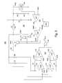
- FIG. 2 illustrates a voltage converter 100 including current-limiting circuitry 102 in accordance with the present invention.
- the voltage converter 100 is coupled to receive power from a power source Vin.
- the source Vin may be, for example, an unregulated direct-current (DC) supply, such as a battery or a rectified alternating current (AC) signal.
- the source Vin may be coupled to a first terminal of a switch SW 3 .
- a second terminal of the switch SW 3 may be coupled to a first terminal of a reactive element, such as an inductor L 2 .
- the second terminal of the switch SW 3 may also be coupled to a first terminal of a switch SW 4 .
- a second terminal of the inductor L 2 may be coupled to a first terminal of a reactive element, such as an output capacitor C 2 .
- a second terminal of the switch SW 4 and a second terminal of the capacitor C 2 may be coupled to a ground node.
- a load 104 coupled across the capacitor C 2 may be powered by the voltage converter 100 .
- the switches SW 3 and SW 4 , the inductor L 2 and the capacitor C 2 form a buck converter power conversion section 106 of the converter 100 .
- the power conversion section 106 is exemplary and that advantages of the invention may be achieved using a power conversion section 106 that has a different topology from that of FIG. 2 .
- the power conversion section 106 may include a boost converter or another type of buck converter.
- a first terminal of a resistor R 3 may be coupled to the first terminal of the capacitor C 2 .
- a second terminal of the resistor R 3 may be coupled to a first terminal of a resistor R 4 .
- a second terminal of the resistor R 4 may be coupled to a second terminal of the capacitor C 2 .
- the resistors R 3 and R 4 form a voltage divider, in which a voltage formed at an intermediate node is proportional to the output voltage Vout 2 .
- This output voltage sensing signal may be coupled to an inverting input of an amplifier 108 .
- a reference voltage Vref 2 may be coupled to a non-inverting input of the amplifier 108 .
- the amplifier 108 forms an error signal Veao 2 that is representative of a difference between the output voltage Vout 2 and a desired level for the output voltage Vout 2 .
- the error signal Veao 2 may be coupled to a non-inverting input of a comparator 110 .
- a periodic ramp signal Vramp 2 formed by an oscillator 112 , may be coupled to an inverting input of the comparator 110 .
- the comparator 110 may form a switch control signal Vsw 2 .
- the switch control signal Vsw 2 may be coupled to the switch SW 3 via a logic AND gate 114 and to the switch SW 4 via an inverter 116 and a logic AND gate 118 .
- the logic gate 114 passes the switch control signal Vsw 2 to the switch SW 3 and the logic gate 118 passes the switch control signal Vsw 2 , as inverted by the inverter 116 , to the switch SW 4 .
- the switch control signal Vsw 2 is a logic high voltage. Under these conditions, the switch SW 3 is closed and the switch SW 4 is open.
- the switch control signal Vsw 2 is a logic low voltage. Under these conditions, the switch SW 3 is open and the switch SW 4 is closed.
- the ramp signal Vramp 2 may rise steadily to a maximum level and then rapidly discharge to a minimum level before the cycle repeats.
- the error signal Veao 2 generally remains between maximum and minimum levels of the ramp signal Vramp 2 .
- the switches SW 3 and SW 4 cycle between opened and closed.
- the output voltage Vout 2 is regulated in a feedback loop.
- the output voltage Vout 2 may be adjusted by adjusting the level of the reference voltage Vref 2 or the values of the resistors R 3 or R 4 .
- control section 120 The resistors R 3 and R 4 , the amplifier 108 , the comparator 110 , oscillator 112 and inverter 116 form a control section 120 of the converter 100 .
- control section 120 is exemplary and that advantages of the invention may be achieved using a control section 120 that differs from that of FIG. 2 .
- input polarities of the amplifier 108 and/or comparator 110 may be exchanged.
- additional elements may be added, such as a latch that forms the switch control signal Vsw 2 based upon the output of the comparator 110 and a clock signal that is synchronous with the ramp signal Vramp 2 .
- the current limiting section 102 of the converter 100 may include a resistor R 5 and a capacitor C 3 .
- a first terminal of the resistor R 5 may be coupled to the first terminal of the inductor L 2 .
- a second terminal of the resistor R 5 may be coupled to a first terminal of a capacitor C 3 .
- a second terminal of the capacitor C 3 may be coupled to the ground node.
- the resistor R 5 and capacitor C 3 form an R-C low-pass filter, in which a signal Vave formed at the node between the resistor R 5 and the capacitor C 3 is representative of an average level of input voltage applied to the first terminal of the inductor L 2 .
- Values for the resistor R 5 and capacitor C 3 are preferably selected such that the signal Vave is representative of an average of the voltage applied to the first terminal of the inductor L 2 over time period of between a few and several cycles of the switch control signal Vsw 2 .
- the current limiting section 102 may also include offset voltage sources Vos 1 , Vos 2 , amplifiers 122 , 124 , comparators 126 , 128 and logic gate 130 .
- the signal Vave may be coupled to a non-inverting input of the amplifier 122 and to an inverting input of the amplifier 124 .
- the second terminal of the inductor L 2 may be coupled to a first terminal of the offset voltage source Vos 1 and to a first terminal of the offset voltage source Vos 2 .
- a second terminal of the offset voltage source Vos 1 may be coupled to an inverting input of the amplifier 122
- a second terminal of the offset voltage source Vos 2 may be coupled to a non-inverting input of an amplifier 124 .
- the amplifier 122 may form a signal Viin 1 at its output, while the amplifier 124 may form a signal Viin 2 at its output.
- An exemplary value for the parasitic resistance of the inductor L 2 is 50 milliohms.
- An exemplary steady-state current drawn by the load 104 and, thus, the average current Iin through the inductor L 2 is 10 amps. Accordingly, the expected voltage drop across the parasitic resistance of the inductor L 2 may be equal to 500 millivolts (50 milliohms ⁇ 10 amps).
- the offset voltage source Vos 1 may be selected to be 500 millivolts, for example, while the offset voltage source Vos 2 may be selected to be ⁇ 500 millivolts, for example.
- the average of the input current Iin is flowing in a forward direction, i.e. from the first terminal of the inductor L 2 to the second terminal of the inductor L 2 .
- the signal Vave may be expected to be approximately 500 millivolts higher than the level at the second terminal of the inductor L 2 due to the voltage drop across the parasitic resistance of the inductor L 2 .
- the offset voltage source Vos 1 may increase the signal level at the second terminal of the inductor L 2 by approximately 500 millivolts.
- the voltage differential applied across inputs of the amplifier 122 is approximately zero volts.
- the signal Viin 1 is representative of a level of current flowing through the inductor L 2 in the forward direction and is expected to be approximately zero volts.
- the signal Viin 2 is representative of a level of current flowing through the inductor L 2 in the reverse direction and is expected to be a negative value below zero. This is because the signal Vave coupled to the inverting input of the amplifier 124 is expected to be approximately 500 millivolts higher than the voltage at the second terminal of the inductor L 2 due to the voltage drop across the inductor L 2 .
- the offset voltage source Vos 2 reduces the signal level at the non-inverting input of the amplifier 124 . As such, the non-inverting input is expected to be approximately 1000 millivolts (1 volt) lower than the voltage at the inverting input.
- the signal Viin 1 at the output of the amplifier 122 may be coupled to a non-inverting input of the comparator 126 .
- a reference voltage Vref 3 may be coupled to an inverting input of the comparator 126 .
- the signal Viin 2 at the output of the amplifier 124 may be coupled to a non-inverting input of the comparator 128 .
- a reference voltage Vref 4 may be coupled to an inverting input of the comparator 128 .
- the output of the comparator 126 may be coupled to a first input of a logic OR gate 130 , while the output of the comparator 128 may be coupled to a second input of the logic OR gate 130 .
- the logic OR gate 130 may form a current-limiting signal Ilimit at its output. When the outputs of the comparators 126 and 128 are both a logic low voltage, then the signal Ilimit may also be a logic low voltage. Accordingly, the AND gate 114 passes the switch control signal Vsw 2 to the switch SW 3 and the logic AND gate 118 passes the inverted switch control signal Vsw 2 to the switch SW 4 . Thus, when the signal Ilimit is logic low voltage, switching in the voltage converter section 106 is enabled.
- the level of Vave rises.
- the signal Viin 1 at the output of the amplifier 122 rises.
- the signal Viin 1 may exceed the level of Vref 3 , which may be set to a level representative of a maximum allowable current so as to avoid damaging elements of the converter 100 .
- the output of the comparator 126 may transition to a logic high voltage, which causes the signal Ilimit to transition to a logic high voltage.
- the switches SW 3 and SW 4 may both be held open until the input current Iin falls sufficiently to cause the signal Viin 1 to fall below the level of Vref 3 .
- the signal Ilimit may return to a logic low voltage and switching of the switches SW 3 and SW 4 may resume.
- switching in the voltage converter section 106 may be disabled.
- Such hysteresis may reduce the frequency in which the input current Iin is interrupted.
- switching may be resumed at a reduced duty-cycle to limit the input current Iin, such as a predetermined minimum duty cycle. This may be achieved by setting the error signal Veao 2 to a predetermined level in response to the signal Ilimit transitioning to a logic high voltage.
- the average input current Iin may be in the reverse direction, i.e. from the second terminal of the inductor L 2 to the first terminal of the inductor L 2 .
- the voltage at the second terminal of the inductor L 2 may exceed the signal Vave due to the parasitic resistance of the inductor L 2 .
- the voltage at the second terminal of the inductor L 2 may exceed the signal Vave by 500 millivolts, assuming a reverse current through the inductor L 2 of 10 amps.
- the signal Viin 1 is expected to be a negative value below zero. This is because the signal Vave coupled to the non-inverting input of the amplifier 122 is expected to be approximately 500 millivolts lower than the voltage at the second terminal of the inductor L 2 due to the voltage drop across the inductor L 2 .
- the offset voltage source Vos 1 increases the signal level at the inverting input of the amplifier 122 . As such, the inverting input is expected to be approximately 1000 millivolts (1 volt) higher than the voltage at the non-inverting input.
- the signal Viin 2 is expected to be around zero volts. This is because the signal Vave may be expected to be approximately 500 millivolts lower than the level at the second terminal of the inductor L 2 due to the voltage drop across the parasitic resistance of the inductor L 2 .
- the offset voltage source Vos 2 may decrease the signal level at the second terminal of the inductor L 2 by approximately 500 millivolts. As such, the voltage differential applied across inputs of the amplifier 124 is approximately zero volts.
- the signal Viin 2 at the output of the amplifier 124 rises.
- the signal Viin 2 may exceed the level of Vref 4 , which may be set to a level representative of a maximum allowable reverse current so as to avoid damaging elements of the converter 100 .
- the output of the comparator 128 may transition to a logic high voltage, which causes the signal Ilimit to transition to a logic high voltage.
- the switches SW 3 and SW 4 may be inhibited from switching until the reverse current Iin falls sufficiently to cause the signal Viin 2 to fall below the level of Vref 4 .
- the signal Ilimit may return to a logic low voltage and switching of the switches SW 3 and SW 4 may resume.
- Hysteresis may also be employed in the comparator 128 so as to cause the current Iin in the inductor L 2 to fall to a level that is a predetermined amount below the reference level before re-enabling switching of the switches SW 3 and SW 4 .
- FIG. 3 illustrates a voltage converter 100 ′ including an alternate embodiment of current-limiting circuitry 102 ′ in accordance with the present invention.
- the current limiting section 102 ′ may include offset voltage sources Vos 1 , Vos 2 , resistors R 6 , R 7 , capacitors C 4 , C 5 , amplifiers 122 , 124 , comparators 126 , 128 and logic gate 130 .
- a first terminal of the resistor R 6 and a first terminal of the resistor R 7 may be coupled to the first terminal of the inductor L 2 .
- a second terminal of the resistor R 6 may be coupled to the non-inverting input of the amplifier 122 and to a first terminal of the capacitor C 4 .
- the output terminal of the amplifier 122 may form a signal Viin 3 and may be coupled to a second terminal of the capacitor C 4 .
- the second terminal of the inductor L 2 may be coupled to a first terminal of the offset voltage source Vos 1 and to a first terminal of the offset voltage source Vos 2 .
- a second terminal of the source Vos 1 may be coupled to the inverting input terminal of the amplifier 122 .
- the amplifier 122 may be configured as an integrator or low-pass filter.
- the signal Viin 3 may be representative of an average voltage across the inductor L 2 , offset by the source Vos 1 .
- the signal Viin 3 may be representative of a level of current flowing in the inductor L 2 in the forward direction.
- the signal Viin 3 is expected to be approximately zero volts.
- the signal Viin 3 may be coupled to a non-inverting input of the comparator 126 , while the reference voltage Vref 3 may be coupled to an inverting input of the comparator 126 .
- the signal Viin 3 may be below the level of Vref 3 .
- the signal Viin 3 may also rise.
- the signal Viin 3 may exceed a level of Vref 3 .
- the output of the comparator 126 may transition to a logic high voltage.
- the current-limiting signal Ilimit may also transition to a logic high voltage, inhibiting switching of the switches SW 3 and SW 4 until the input current Iin falls sufficiently that the output of the comparator 126 returns to a logic low voltage.
- a second terminal of the resistor R 7 may be coupled to the inverting input of the amplifier 124 and to a first terminal of the capacitor C 5 .
- the output terminal of the amplifier 124 may form a signal Viin 4 and may be coupled to a second terminal of the capacitor C 5 .
- a second terminal of the offset voltage source Vos 2 may be coupled to the inverting input terminal of the amplifier 124 .
- the amplifier 124 may be configured as an integrator or low-pass filter.
- the signal Viin 4 may be representative of an average voltage across the inductor L 2 , offset by the source Vos 2 .
- the signal Viin 4 may be representative of a level of current flowing the inductor L 2 in the reverse direction. Under exemplary reverse-current conditions where 10 amps of current flows from the second terminal of the inductor L 2 to the first terminal of the inductor L 2 , the signal Viin 4 is expected to be approximately zero volts.
- the signal Viin 4 may be coupled to a non-inverting input of the comparator 128 , while the reference voltage Vref 4 may be coupled to an inverting input of the comparator 128 .
- the signal Viin 4 may be below the level of Vref 4 .
- the signal Viin 4 may also rise.
- the signal Viin 4 may exceed a level of Vref 4 .
- the output of the comparator 128 may transition to a logic high voltage.
- the current-limiting signal Ilimit may also transition logic high voltage, inhibiting switching of the switches SW 3 and SW 4 until the reverse current Iin falls sufficiently that the output of the comparator 128 returns to a logic low voltage.
- FIG. 4 illustrates a voltage converter 400 including an alternate embodiment of current-limiting circuitry 402 in accordance with the present invention.
- the resistors R 3 and R 4 form a voltage divider, in which a voltage formed at an intermediate node is proportional to the output voltage Vout 2 .
- This output voltage signal may be coupled to an inverting input of an amplifier 408 .
- a reference voltage Vref 2 may be coupled to a non-inverting input of the amplifier 408 .
- the amplifier 408 forms an error signal Veao 2 that is representative of a difference between the output voltage Vout 2 and a desired level for the output voltage Vout 2 .
- the error signal Veao 2 may be coupled to a first inverting input of multi-input comparator 410 .
- a periodic ramp signal Vramp 2 formed by an oscillator 112 , may be coupled to a non-inverting input of the comparator 410 .
- the comparator 410 may form a switch control signal Vsw 2 .
- the switch control signal Vsw 2 may be coupled to a switch SW 4 and to an input of inverter 414 .
- the output of inverter 414 may be coupled to a switch SW 3 .
- a control section 420 of the converter 400 may include: the resistor R 3 ; the resistor R 4 ; the amplifier 408 ; the multi-input comparator 410 ; the oscillator 112 ; and the inverter 414 .
- the voltage control section 420 is exemplary and that advantages of the invention may be achieved by using control section 420 that differs from that of FIG. 4 .
- input polarities of the amplifier 408 and/or comparator 410 may be exchanged.
- additional elements may be included, such as a latch that forms the switch control signal Vsw 2 based upon the output of the comparator 410 and a clock signal that is synchronous with the ramp signal Vramp 2 .
- the current limiting section 402 may include: a resistor R 5 ; a capacitor C 3 ; a offset voltage source Vos 1 ; a offset voltage source Vos 2 , an amplifier 422 ; an amplifier 424 ; the multi-input comparator 410 , and the inverter 414 .
- the comparator 410 and the inverter 414 maybe shared with the voltage control section 420 .
- the signal Vave that is representative of the input current may be coupled to an inverting input of the amplifier 422 and to a non-inverting input of the amplifier 424 .
- the second terminal of the inductor L 2 may be coupled to a first terminal of the offset voltage source Vos 1 and to a first terminal of the offset voltage source Vos 2 .
- a second terminal of the offset voltage source Vos 1 may be coupled to a non-inverting input of the amplifier 422 .
- a second terminal of the offset voltage source Vos 2 may be coupled to an inverting input of an amplifier 424 .
- the amplifier 422 may form a signal Viin 1 at its output, while the amplifier 424 may form a signal Viin 2 at its output.
- the signal Viin 1 is representative of the forward current passing through the inductor L 2 relative to the offset voltage Vos 1 .
- the signal Viin 2 is representative of the reverse current passing through the inductor relative to the offset voltage Vos 2 . It will be apparent that the circuitry by which a current passing through the inductor L 2 is measured may be altered from that shown in FIG. 4 and still achieve the principal objects of the invention. For example, a sensing resistor in series with the inductor L 2 may be used to measure the current passing through the inductor L 2 .
- the signal Viin 1 at the output of the amplifier 422 may be coupled to a second inverting input of the comparator 410 . If the reverse current is to be monitored, the signal Viin 2 at the output of the amplifier 424 may be coupled to a third inverting input of the comparator 410 .
- Multi-input comparator 410 may operate such that whichever inverted input is the lowest is compared to the non-inverted input for controlling its output. Thus, when the lowest inverted input is higher than the non-inverted input then the output of the multi-input comparator 410 is a logic low voltage. Also, when the lowest inverted input is lower than the non-inverted input then the output of the multi-input comparator 410 is a logic high voltage.
- the switch control signal Vsw 2 is a logic low voltage. Under these conditions, the switch SW 3 is closed and the switch SW 4 is open. Whenever a lowest one of Veao 2 , Viin 1 , and Viin 2 is lower than the ramp signal Vramp 2 , the switch control signal Vsw 2 is a logic high voltage. Under these conditions, the switch SW 3 is open and the switch SW 4 is closed.
- the ramp signal Vramp 2 may rise steadily to a maximum level and then rapidly discharge to a minimum level before the cycle repeats.
- the error signal Veao 2 generally remains between maximum and minimum levels of the ramp signal Vramp 2 .
- the switches SW 3 and SW 4 cycle between opened and closed.
- the duty cycle of the switch SW 3 (and the switch SW 4 ) is controlled in a feedback loop based on the error signal Veao 2 so as to maintain the output voltage Vout at its desired level.
- Viin 2 or Viin 1 When an overcurrent condition occurs, either Viin 2 or Viin 1 will be less than Veao 2 . This will cause the duty cycle of Vsw 3 to decrease. Decreasing the duty cycle of the switch SW 3 tends to reduce the input current. As the current in the inductor L 2 increases, the switching duty cycle is gradually reduced (via the switch control signal Vsw 3 ). This technique allows the voltage regulator to gradually decrease the duty cycle and, thus, the input current is reduced when the input current is excessive. This is in contrast to the embodiments of FIGS. 2 and 3 in which switching is disabled when the input current is excessive. However, if Viin 2 or Viin 1 are less then the minimum ramp signal level 112 , or otherwise fall outside the ramp signal maximum and minimum levels, then the input incurrent may be inhibited by disabling switching.
- the switching duty cycle is set to a minimum value instead of disabling it completely when Viin 2 or Viin 1 reach a predetermined level. This may be accomplished, for example, by constraining the levels of Viin 2 and Viin 1 .
- FIG. 5 illustrates a voltage converter 500 including an alternate embodiment of a current-limiting circuitry 502 in accordance with the present invention.
- the current limiting section 502 may include: the offset voltage source Vos 1 ; the offset voltage source Vos 2 ; a resistor R 6 ; a resistor R 7 ; a capacitor C 4 ; a capacitor C 5 ; an amplifier 522 ; an amplifier 524 , a multi-input comparator 410 , the inverter 414 .
- the comparator 410 and the inverter 414 maybe shared with the voltage control section 420 .
- a first terminal of the resistor R 6 and a first terminal of the resistor R 7 may be coupled to a first terminal of the inductor L 2 .
- a second terminal of the resistor R 6 may be coupled to an inverting input of the amplifier 522 and to a first terminal of the capacitor C 4 .
- a second terminal of the inductor L 2 may be coupled to a first terminal of the offset voltage source Vos 1 and to a first terminal of the offset voltage source Vos 2 .
- a second terminal of the source Vos 1 may be coupled to an non-inverting input terminal of the amplifier 522 .
- An output terminal of the amplifier 522 may be coupled to a second terminal of the capacitor C 4 .
- An output terminal of the amplifier 522 may form the signal Viin 3 .
- the amplifier 522 may be configured as an integrator or low-pass filter.
- the signal Viin 3 may be representative of an average voltage across the inductor L 2 , offset by the source Vos 1 .
- the signal Viin 3 may be representative of a level of current flowing through the inductor L 2 in the forward direction.
- the signal Viin 3 may be coupled to the second inverting input of multi-input comparator 410 .
- a second terminal of the resistor R 7 may be coupled to a non-inverting input of the amplifier 524 and to a first terminal of the capacitor C 5 .
- a second terminal of the offset voltage source Vos 2 may be coupled to an inverting input terminal of the amplifier 524 .
- the output terminal of the amplifier 524 may be coupled to a second terminal of the capacitor C 5 .
- the output terminal of the amplifier 524 may form a signal Viin 4 .
- the amplifier 524 may be configured as an integrator or low-pass filter.
- the signal Viin 4 may be representative of an average voltage across the inductor L 2 , offset by the source Vos 2 .
- the signal Viin 4 may be representative of a level of current flowing through the inductor L 2 in the reverse direction.
- the signal Viin 4 may be coupled to an inverting input of multi-input comparator 510 .
- the voltage control section 420 of FIG. 5 may be the same as in FIG. 4 .
- Viin 3 or Viin 4 will be less than Veao 2 . This will cause the duty cycle of Vsw 3 to decrease. Decreasing the duty cycle of the switch SW 3 tends to reduce the input current. As the current in the inductor increases, the switching duty cycle will be gradually reduced (via the switch control signal Vsw 3 ).
- This technique allows the voltage regulator to gradually decrease the duty cycle and, thus, the input current is reduced when the input current is excessive. This is in contrast to the embodiments of FIGS. 2 and 3 in which the switching is disabled when the current is excessive.
- Viin 3 or Viin 4 are less then the minimum ramp signal level 112 , or otherwise fall outside the ramp signal maximum and minimum levels, then the input current may be inhibited by disabling switching.
- the switching duty cycle may be set to a minimum value instead of disabling it completely.
- FIG. 6 illustrates an exemplary implementation of the multi-input comparator 410 of FIGS. 5 and 6.
- An output of a current source 601 may be coupled to: an emitter of pnp transistor 606 ; an emitter of pnp transistor 607 ; an emitter of pnp transistor 608 ; and an emitter of pnp transistor 609 .
- An output of a current source 602 may be coupled to the collector of an npn transistor 603 and to an output of the comparator 410 , which forms the switch control signal Vsw 2 .
- An inverted input that receives the signal Viin 4 may be coupled to the base of the pnp transistor 606 .
- An inverted input that receives the signal Viin 3 may be coupled to the base of pnp transistor 609 .
- An inverted input that receives the signal Veao 2 may be coupled to the base of pnp transistor 607 .
- a non-inverted input Vramp 2 may be coupled to the base of pnp transistor 608 .
- the collectors of pnp transistors 606 , 607 and 609 may be tied together and coupled to a collector and a base of an npn transistor 605 and to a base of an npn transistor 604 .
- a collector of the pnp transistor 608 may be coupled to a base of the npn transistor 603 and to a collector of the npn transistor 604 .
- the emitters of the npn transistors 603 , 604 and 605 may be tied ground.
- Vsw 2 is a logic high voltage when the Vramp 2 input is greater than the lowest one of Viin 3 , Viin 4 and Veao 2 .
- Vsw 2 is a logic low voltage when the Vramp 2 input is lower than the lowest one of Viin 3 , Viin 4 and Veao 2 .
Abstract
A current limiting technique for a voltage converter. A current through a reactive element in a voltage converter is limited. Current from a supply is switched through a reactive element in accordance with a switch control signal for forming a regulated output voltage in a feedback loop. A first signal that is representative of the input current is sensed. A voltage that is representative of the output voltage of the voltage converter is sensed. A second signal that is representative of a difference between the output voltage and a desired voltage is formed. A selected one of the first signal and the second signal is compared to a ramp signal for forming the switch control signal wherein the selected one of the first signal and the second signal is selected according to the relative magnitudes of the first and second signal.
Description
This is a continuation-in-part of U.S. application Ser. No. 09/823,836, filed Mar. 30, 2001.
The present invention relates to the field of voltage converters. More particularly, the present invention relates to prevention of over-current conditions in voltage converters.
In a conventional voltage converter, an output voltage is typically monitored, compared to a predetermined desired level and a response is developed to more precisely attain the desired output voltage. More particularly, to adjust the output voltage, the input current is modulated up or down. Conventional modulation techniques include pulse-width modulation (PWM) and frequency modulation.
FIG. 1 illustrates a voltage converter of the prior art. An unregulated direct-current DC voltage source Vin1 is coupled to a first terminal of a switch SW1. A second terminal of the switch SW1 is coupled to a first terminal of an inductor L1 and to a first terminal of a switch SW2. A second terminal of the inductor L1 is coupled to a first terminal of an output capacitor C1. A second terminal of the switch SW2 and a second terminal of the capacitor C1 are coupled to ground.
When the switch SW1 is closed, the switch SW2 is open. Under these conditions, current flows from the input source Vin1 through the inductor L1 and charges the capacitor C1. Thus, an output voltage Vout1 formed across the capacitor C1 tends to increase. When the switch SW1 is open, the switch SW2 is closed. Under these conditions, current from the capacitor C1 flows through the inductor L1 and to ground. Thus, the output voltage Vout1 tends to decrease. A load 10 coupled across the capacitor C1 is powered by the voltage converter.
A first terminal of a resistor R1 is coupled to the first terminal of the capacitor C1. A second terminal of the resistor R1 is coupled to a first terminal of a resistor R2. A second terminal of the resistor R2 is second terminal of the capacitor C1.
The resistors R1 and R2 form a voltage divider, in which a voltage formed at an intermediate node is proportional to the output voltage Vout1. This voltage is coupled to an inverting input of an amplifier 12. A reference voltage Vref1 is coupled to a non-inverting input of the amplifier 12. The amplifier 12 forms an error signal Veao1 that is representative of a difference between the output voltage Vout1 and a desired level for the output voltage Vout1.
The error signal Veao1 is coupled to a non-inverting input of a comparator 14. A periodic ramp signal Vramp1 formed by an oscillator 16 is coupled to an inverting input of the comparator 14. The comparator 14 forms a switch control signal Vsw1 that is coupled to the switch SW1 and to an input of an inverter 18. An output of the inverter 18 is coupled to the switch SW2.
As can be seen from FIG. 1, when the error signal Veao1 is higher than the ramp signal Vramp1, the switch control signal Vsw1 is a logic high voltage. Under these conditions, the switch SW1 is closed and the switch SW2 is open. When the error signal Veao1 is lower than the ramp signal Vramp1, the switch control signal Vsw1 is a logic low voltage. Under these conditions, the switch SW1 is open and the switch SW2 is closed.
The ramp signal Vramp1 rises steadily to a maximum level and then rapidly discharges to a minimum level before the cycle repeats. The error signal Veao1 generally remains between maximum and minimum levels of the ramp signal Vramp1. Thus, for each cycle of the ramp signal Vramp1, the switches SW1 and SW2 cycle between opened and closed.
When the output voltage Vout1 decreases, the error signal Veao1 increases. This increases the duty cycle for the switch SW1 and, thus, increases the output voltage Vout1. When the output voltage Vout1 increases, the error signal Veao1 decreases. This decreases the duty cycle for the switch SW1 and, thus, decreases the output voltage Vout1. Accordingly, the output voltage Vout1 is regulated in a feedback loop.
If the output voltage Vout1 is significantly below the desired level, then the switch SW1 may be closed for a significant portion of the time. As a result, the input current can be of a large magnitude. Further, if the input voltage Vin1 should rise unexpectedly, this can also contribute to a large input current. A large input current may cause damage to elements of the converter, such as the switch SW1. Accordingly, it may be desirable to provide a technique for limiting the input current to the converter.
Therefore, what is needed is a technique for limiting the input current to a voltage converter. It is to these ends that the present invention is directed.
The invention is a current limiting technique for a voltage converter. The level of input current to the converter is determined. If the measured current level is excessive, then switching in the converter may be interrupted or the duty cycle reduced until the current falls to an acceptable level. Because parasitic resistance may be used to detect the input current, rather than a dedicated sensing resistor, fewer components may be required. Thus, implementation of the converter and its associated control circuitry is simplified.
In accordance with one aspect of the invention, a current through a reactive element in a voltage converter is limited. Current from a supply is switched through a reactive element in accordance with a switch control signal for forming a regulated output voltage in a feedback loop. A first signal that is representative of the input current is sensed. A voltage that is representative of the output voltage of the voltage converter is sensed. A second signal that is representative of a difference between the output voltage and a desired voltage is formed. A selected one of the first signal and the second signal is compared to a ramp signal for forming the switch control signal wherein the selected one of the first signal and the second signal is selected according to the relative magnitudes of the first and second signal.
FIG. 1 illustrates a voltage converter of the prior art;
FIG. 2 illustrates a voltage converter including current-limiting circuitry in accordance with an embodiment of the present invention that disables the switching current;
FIG. 3 illustrates a voltage converter including an alternate embodiment of current-limiting circuitry in accordance with the present invention;
FIG. 4 illustrates a voltage converter including current-limiting circuitry in accordance with an embodiment of the present invention that decrease the duty cycle;
FIG. 5 illustrates a voltage converter including an alternate embodiment of current-limiting circuitry in accordance with an embodiment of the present invention that decrease the duty cycle; and
FIG. 6 illustrates an exemplary implementation of a multi-input comparator in accordance with an aspect of the present invention.
FIG. 2 illustrates a voltage converter 100 including current-limiting circuitry 102 in accordance with the present invention. The voltage converter 100 is coupled to receive power from a power source Vin. The source Vin may be, for example, an unregulated direct-current (DC) supply, such as a battery or a rectified alternating current (AC) signal. The source Vin may be coupled to a first terminal of a switch SW3. A second terminal of the switch SW3 may be coupled to a first terminal of a reactive element, such as an inductor L2. The second terminal of the switch SW3 may also be coupled to a first terminal of a switch SW4. A second terminal of the inductor L2 may be coupled to a first terminal of a reactive element, such as an output capacitor C2. A second terminal of the switch SW4 and a second terminal of the capacitor C2 may be coupled to a ground node.
When the switch SW3 is closed, the switch SW4 is open. Under these conditions, an input current Iin flows from the input source Vin through the inductor L2 and charges the capacitor C2. Thus, an output voltage Vout2 formed across the capacitor C2 tends to increase. When the switch SW3 is open, the switch SW4 is closed. Under these conditions, current from the capacitor C2 flows through the inductor L2 and to ground. Thus, the output voltage Vout2 tends to decrease. A load 104 coupled across the capacitor C2 may be powered by the voltage converter 100.
The switches SW3 and SW4, the inductor L2 and the capacitor C2 form a buck converter power conversion section 106 of the converter 100. It will be apparent that the power conversion section 106 is exemplary and that advantages of the invention may be achieved using a power conversion section 106 that has a different topology from that of FIG. 2. For example, the power conversion section 106 may include a boost converter or another type of buck converter.
A first terminal of a resistor R3 may be coupled to the first terminal of the capacitor C2. A second terminal of the resistor R3 may be coupled to a first terminal of a resistor R4. A second terminal of the resistor R4 may be coupled to a second terminal of the capacitor C2.
The resistors R3 and R4 form a voltage divider, in which a voltage formed at an intermediate node is proportional to the output voltage Vout2. This output voltage sensing signal may be coupled to an inverting input of an amplifier 108. A reference voltage Vref2 may be coupled to a non-inverting input of the amplifier 108. The amplifier 108 forms an error signal Veao2 that is representative of a difference between the output voltage Vout2 and a desired level for the output voltage Vout2.
The error signal Veao2 may be coupled to a non-inverting input of a comparator 110. A periodic ramp signal Vramp2, formed by an oscillator 112, may be coupled to an inverting input of the comparator 110. The comparator 110 may form a switch control signal Vsw2. The switch control signal Vsw2 may be coupled to the switch SW3 via a logic AND gate 114 and to the switch SW4 via an inverter 116 and a logic AND gate 118.
Under normal operating conditions, in absence of an over-current condition, the logic gate 114 passes the switch control signal Vsw2 to the switch SW3 and the logic gate 118 passes the switch control signal Vsw2, as inverted by the inverter 116, to the switch SW4. Thus, when the error signal Veao2 is higher than the ramp signal Vramp2, the switch control signal Vsw2 is a logic high voltage. Under these conditions, the switch SW3 is closed and the switch SW4 is open. When the error signal Veao2 is lower than the ramp signal Vramp2, the switch control signal Vsw2 is a logic low voltage. Under these conditions, the switch SW3 is open and the switch SW4 is closed.
The ramp signal Vramp2 may rise steadily to a maximum level and then rapidly discharge to a minimum level before the cycle repeats. The error signal Veao2 generally remains between maximum and minimum levels of the ramp signal Vramp2. Thus, for each cycle of the ramp signal Vramp2, the switches SW3 and SW4 cycle between opened and closed.
When the output voltage Vout2 decreases, the error signal Veao2 increases. This increases the duty cycle for the switch SW3 and, thus, increases the output voltage Vout2. When the output voltage Vout2 increases, the error signal Veao2 decreases. This decreases the duty cycle for the switch SW3 and, thus, decreases the output voltage Vout2. Accordingly, the output voltage Vout2 is regulated in a feedback loop. The output voltage Vout2 may be adjusted by adjusting the level of the reference voltage Vref2 or the values of the resistors R3 or R4.
The resistors R3 and R4, the amplifier 108, the comparator 110, oscillator 112 and inverter 116 form a control section 120 of the converter 100. It will be apparent that the control section 120 is exemplary and that advantages of the invention may be achieved using a control section 120 that differs from that of FIG. 2. For example, input polarities of the amplifier 108 and/or comparator 110 may be exchanged. As another example, additional elements may be added, such as a latch that forms the switch control signal Vsw2 based upon the output of the comparator 110 and a clock signal that is synchronous with the ramp signal Vramp2.
The current limiting section 102 of the converter 100 may include a resistor R5 and a capacitor C3. A first terminal of the resistor R5 may be coupled to the first terminal of the inductor L2. A second terminal of the resistor R5 may be coupled to a first terminal of a capacitor C3. A second terminal of the capacitor C3 may be coupled to the ground node. The resistor R5 and capacitor C3 form an R-C low-pass filter, in which a signal Vave formed at the node between the resistor R5 and the capacitor C3 is representative of an average level of input voltage applied to the first terminal of the inductor L2. Values for the resistor R5 and capacitor C3 are preferably selected such that the signal Vave is representative of an average of the voltage applied to the first terminal of the inductor L2 over time period of between a few and several cycles of the switch control signal Vsw2.
The current limiting section 102 may also include offset voltage sources Vos1, Vos2, amplifiers 122, 124, comparators 126, 128 and logic gate 130. The signal Vave may be coupled to a non-inverting input of the amplifier 122 and to an inverting input of the amplifier 124. The second terminal of the inductor L2 may be coupled to a first terminal of the offset voltage source Vos1 and to a first terminal of the offset voltage source Vos2. A second terminal of the offset voltage source Vos1 may be coupled to an inverting input of the amplifier 122, while a second terminal of the offset voltage source Vos2 may be coupled to a non-inverting input of an amplifier 124. The amplifier 122 may form a signal Viin1 at its output, while the amplifier 124 may form a signal Viin2 at its output.
An exemplary value for the parasitic resistance of the inductor L2 is 50 milliohms. An exemplary steady-state current drawn by the load 104 and, thus, the average current Iin through the inductor L2, is 10 amps. Accordingly, the expected voltage drop across the parasitic resistance of the inductor L2 may be equal to 500 millivolts (50 milliohms×10 amps). Based on these exemplary values, the offset voltage source Vos1 may be selected to be 500 millivolts, for example, while the offset voltage source Vos2 may be selected to be −500 millivolts, for example.
When the load 104 is drawing steady-state current, the average of the input current Iin is flowing in a forward direction, i.e. from the first terminal of the inductor L2 to the second terminal of the inductor L2. Under these conditions, the signal Vave may be expected to be approximately 500 millivolts higher than the level at the second terminal of the inductor L2 due to the voltage drop across the parasitic resistance of the inductor L2. The offset voltage source Vos1 may increase the signal level at the second terminal of the inductor L2 by approximately 500 millivolts. As such, the voltage differential applied across inputs of the amplifier 122 is approximately zero volts. Accordingly, the signal Viin1 is representative of a level of current flowing through the inductor L2 in the forward direction and is expected to be approximately zero volts.
Under these conditions, the signal Viin2 is representative of a level of current flowing through the inductor L2 in the reverse direction and is expected to be a negative value below zero. This is because the signal Vave coupled to the inverting input of the amplifier 124 is expected to be approximately 500 millivolts higher than the voltage at the second terminal of the inductor L2 due to the voltage drop across the inductor L2. The offset voltage source Vos2 reduces the signal level at the non-inverting input of the amplifier 124. As such, the non-inverting input is expected to be approximately 1000 millivolts (1 volt) lower than the voltage at the inverting input.
The signal Viin1 at the output of the amplifier 122 may be coupled to a non-inverting input of the comparator 126. A reference voltage Vref3 may be coupled to an inverting input of the comparator 126. The signal Viin2 at the output of the amplifier 124 may be coupled to a non-inverting input of the comparator 128. A reference voltage Vref4 may be coupled to an inverting input of the comparator 128. Thus, under the above-described conditions in which the load 104 draws a steady-state current, the signal Viin1 may be below the level of Vref3, while the signal Viin2 may be below the level of Vref4. Accordingly, the outputs of the comparators 126 and 128 may both be a logic low voltage.
The output of the comparator 126 may be coupled to a first input of a logic OR gate 130, while the output of the comparator 128 may be coupled to a second input of the logic OR gate 130. The logic OR gate 130 may form a current-limiting signal Ilimit at its output. When the outputs of the comparators 126 and 128 are both a logic low voltage, then the signal Ilimit may also be a logic low voltage. Accordingly, the AND gate 114 passes the switch control signal Vsw2 to the switch SW3 and the logic AND gate 118 passes the inverted switch control signal Vsw2 to the switch SW4. Thus, when the signal Ilimit is logic low voltage, switching in the voltage converter section 106 is enabled.
Should the average current Iin through the inductor L2 exceed its steady-state level, the level of Vave rises. As a result, the signal Viin1 at the output of the amplifier 122 rises. Eventually, the signal Viin1 may exceed the level of Vref3, which may be set to a level representative of a maximum allowable current so as to avoid damaging elements of the converter 100. When this occurs, the output of the comparator 126 may transition to a logic high voltage, which causes the signal Ilimit to transition to a logic high voltage. As a result, the switches SW3 and SW4 may both be held open until the input current Iin falls sufficiently to cause the signal Viin1 to fall below the level of Vref3. When the input current falls sufficiently, the signal Ilimit may return to a logic low voltage and switching of the switches SW3 and SW4 may resume. Thus, when the signal Ilimit is logic high voltage, switching in the voltage converter section 106 may be disabled.
Thus, a technique for limiting the input current Iin in the power conversion section 106 has been described, in which the input current Iin is sensed by monitoring an average voltage across the inductor L2. It will be apparent that the circuitry by which switching is disabled, e.g., current limiting section 102 and logic AND gates 114 and 118, may be altered from that shown in FIG. 2, while still achieving the principal objects of the invention. For example, hysteresis may be employed in the comparator 126 so as to cause the current Iin in the inductor L2 to fall to a level that is a predetermined amount below the reference level before re-enabling switching of the switches SW3 and SW4. Such hysteresis may reduce the frequency in which the input current Iin is interrupted. As another example, rather than disabling switching entirely in response to an over-current condition, switching may be resumed at a reduced duty-cycle to limit the input current Iin, such as a predetermined minimum duty cycle. This may be achieved by setting the error signal Veao2 to a predetermined level in response to the signal Ilimit transitioning to a logic high voltage.
Further, under conditions where the output voltage Vout2 exceeds the predetermined desired level, the average input current Iin may be in the reverse direction, i.e. from the second terminal of the inductor L2 to the first terminal of the inductor L2. As a result, the voltage at the second terminal of the inductor L2 may exceed the signal Vave due to the parasitic resistance of the inductor L2. For example, the voltage at the second terminal of the inductor L2 may exceed the signal Vave by 500 millivolts, assuming a reverse current through the inductor L2 of 10 amps.
Under these conditions, the signal Viin1 is expected to be a negative value below zero. This is because the signal Vave coupled to the non-inverting input of the amplifier 122 is expected to be approximately 500 millivolts lower than the voltage at the second terminal of the inductor L2 due to the voltage drop across the inductor L2. The offset voltage source Vos1 increases the signal level at the inverting input of the amplifier 122. As such, the inverting input is expected to be approximately 1000 millivolts (1 volt) higher than the voltage at the non-inverting input.
However, the signal Viin2 is expected to be around zero volts. This is because the signal Vave may be expected to be approximately 500 millivolts lower than the level at the second terminal of the inductor L2 due to the voltage drop across the parasitic resistance of the inductor L2. The offset voltage source Vos2 may decrease the signal level at the second terminal of the inductor L2 by approximately 500 millivolts. As such, the voltage differential applied across inputs of the amplifier 124 is approximately zero volts.
Should the average reverse current Iin through the inductor L2 continue to rise, the signal Viin2 at the output of the amplifier 124 rises. Eventually, the signal Viin2 may exceed the level of Vref4, which may be set to a level representative of a maximum allowable reverse current so as to avoid damaging elements of the converter 100. When this occurs, the output of the comparator 128 may transition to a logic high voltage, which causes the signal Ilimit to transition to a logic high voltage. As a result, the switches SW3 and SW4 may be inhibited from switching until the reverse current Iin falls sufficiently to cause the signal Viin2 to fall below the level of Vref4. When the input current falls sufficiently, the signal Ilimit may return to a logic low voltage and switching of the switches SW3 and SW4 may resume.
Thus, a technique for limiting the input current fin flowing in the reverse direction in the power conversion section 106 by monitoring an average voltage across the inductor L2 has been described. Hysteresis may also be employed in the comparator 128 so as to cause the current Iin in the inductor L2 to fall to a level that is a predetermined amount below the reference level before re-enabling switching of the switches SW3 and SW4.
FIG. 3 illustrates a voltage converter 100′ including an alternate embodiment of current-limiting circuitry 102′ in accordance with the present invention. As shown in FIG. 3, the current limiting section 102′ may include offset voltage sources Vos1, Vos2, resistors R6, R7, capacitors C4, C5, amplifiers 122, 124, comparators 126, 128 and logic gate 130. A first terminal of the resistor R6 and a first terminal of the resistor R7 may be coupled to the first terminal of the inductor L2.
A second terminal of the resistor R6 may be coupled to the non-inverting input of the amplifier 122 and to a first terminal of the capacitor C4. The output terminal of the amplifier 122 may form a signal Viin3 and may be coupled to a second terminal of the capacitor C4. The second terminal of the inductor L2 may be coupled to a first terminal of the offset voltage source Vos1 and to a first terminal of the offset voltage source Vos2. A second terminal of the source Vos1 may be coupled to the inverting input terminal of the amplifier 122.
Accordingly, the amplifier 122 may be configured as an integrator or low-pass filter. As such, the signal Viin3 may be representative of an average voltage across the inductor L2, offset by the source Vos1. Thus, the signal Viin3 may be representative of a level of current flowing in the inductor L2 in the forward direction. Under exemplary steady-state conditions where the load 104 draws 10 amps of current and the offset source Vos1 is approximately equal to a voltage expected across parasitic resistance of the inductor L2, i.e. 500 millivolts, the signal Viin3 is expected to be approximately zero volts.
The signal Viin3 may be coupled to a non-inverting input of the comparator 126, while the reference voltage Vref3 may be coupled to an inverting input of the comparator 126. Thus, under the above-described conditions in which the load 104 draws a steady-state current, the signal Viin3 may be below the level of Vref3. However, should the input current Iin rise, then the signal Viin3 may also rise. Eventually, the signal Viin3 may exceed a level of Vref3. In which case, the output of the comparator 126 may transition to a logic high voltage. As a result, the current-limiting signal Ilimit may also transition to a logic high voltage, inhibiting switching of the switches SW3 and SW4 until the input current Iin falls sufficiently that the output of the comparator 126 returns to a logic low voltage.
Similarly, a second terminal of the resistor R7 may be coupled to the inverting input of the amplifier 124 and to a first terminal of the capacitor C5. The output terminal of the amplifier 124 may form a signal Viin4 and may be coupled to a second terminal of the capacitor C5. A second terminal of the offset voltage source Vos2 may be coupled to the inverting input terminal of the amplifier 124.
Accordingly, the amplifier 124 may be configured as an integrator or low-pass filter. As such, the signal Viin4 may be representative of an average voltage across the inductor L2, offset by the source Vos2. Thus, the signal Viin4 may be representative of a level of current flowing the inductor L2 in the reverse direction. Under exemplary reverse-current conditions where 10 amps of current flows from the second terminal of the inductor L2 to the first terminal of the inductor L2, the signal Viin4 is expected to be approximately zero volts.
The signal Viin4 may be coupled to a non-inverting input of the comparator 128, while the reference voltage Vref4 may be coupled to an inverting input of the comparator 128. Thus, under the above-described conditions, the signal Viin4 may be below the level of Vref4. However, should the reverse current Iin rise, then the signal Viin4 may also rise. Eventually, the signal Viin4 may exceed a level of Vref4. In which case, the output of the comparator 128 may transition to a logic high voltage. As a result, the current-limiting signal Ilimit may also transition logic high voltage, inhibiting switching of the switches SW3 and SW4 until the reverse current Iin falls sufficiently that the output of the comparator 128 returns to a logic low voltage.
Thus, an alternate technique for limiting the input current Iin in the power conversion section 106 has been described, in which the input current Iin is sensed by monitoring an average voltage across the inductor L2. It will be apparent that the circuitry by which switching is inhibited, e.g., current limiting section 102′ and logic AND gates 114 and 118, may be altered from that shown in FIG. 3, while still achieving the principal objects of the invention. For example, hysteresis may be employed in the comparators 126 and 128 so as to cause the current Iin in the inductor L2 to fall to a level that is somewhat below the predetermined level before re-enabling switching of the switches SW3 and SW4. As another example, rather than disabling switching entirely in response to an over-current condition, switching may be resumed at a reduced duty-cycle, such as a predetermined minimum duty cycle.
FIG. 4 illustrates a voltage converter 400 including an alternate embodiment of current-limiting circuitry 402 in accordance with the present invention.
The resistors R3 and R4 form a voltage divider, in which a voltage formed at an intermediate node is proportional to the output voltage Vout2. This output voltage signal may be coupled to an inverting input of an amplifier 408. A reference voltage Vref2 may be coupled to a non-inverting input of the amplifier 408. The amplifier 408 forms an error signal Veao2 that is representative of a difference between the output voltage Vout2 and a desired level for the output voltage Vout2.
The error signal Veao2 may be coupled to a first inverting input of multi-input comparator 410. A periodic ramp signal Vramp2, formed by an oscillator 112, may be coupled to a non-inverting input of the comparator 410. The comparator 410 may form a switch control signal Vsw2. The switch control signal Vsw2 may be coupled to a switch SW4 and to an input of inverter 414. The output of inverter 414 may be coupled to a switch SW3.
A control section 420 of the converter 400 may include: the resistor R3; the resistor R4; the amplifier 408; the multi-input comparator 410; the oscillator 112; and the inverter 414. It will be apparent that the voltage control section 420 is exemplary and that advantages of the invention may be achieved by using control section 420 that differs from that of FIG. 4. For example, input polarities of the amplifier 408 and/or comparator 410 may be exchanged. As another example, additional elements may be included, such as a latch that forms the switch control signal Vsw2 based upon the output of the comparator 410 and a clock signal that is synchronous with the ramp signal Vramp2.
The current limiting section 402 may include: a resistor R5; a capacitor C3; a offset voltage source Vos1; a offset voltage source Vos2, an amplifier 422; an amplifier 424; the multi-input comparator 410, and the inverter 414. The comparator 410 and the inverter 414 maybe shared with the voltage control section 420.
The signal Vave that is representative of the input current may be coupled to an inverting input of the amplifier 422 and to a non-inverting input of the amplifier 424. The second terminal of the inductor L2 may be coupled to a first terminal of the offset voltage source Vos1 and to a first terminal of the offset voltage source Vos2. A second terminal of the offset voltage source Vos1 may be coupled to a non-inverting input of the amplifier 422. A second terminal of the offset voltage source Vos2 may be coupled to an inverting input of an amplifier 424. The amplifier 422 may form a signal Viin1 at its output, while the amplifier 424 may form a signal Viin2 at its output. The signal Viin1 is representative of the forward current passing through the inductor L2 relative to the offset voltage Vos1. The signal Viin2 is representative of the reverse current passing through the inductor relative to the offset voltage Vos2. It will be apparent that the circuitry by which a current passing through the inductor L2 is measured may be altered from that shown in FIG. 4 and still achieve the principal objects of the invention. For example, a sensing resistor in series with the inductor L2 may be used to measure the current passing through the inductor L2.
The signal Viin1 at the output of the amplifier 422 may be coupled to a second inverting input of the comparator 410. If the reverse current is to be monitored, the signal Viin2 at the output of the amplifier 424 may be coupled to a third inverting input of the comparator 410.
Thus, whenever a lowest one of Veao2, Viin1, and Viin2 is higher than the ramp signal Vramp2, the switch control signal Vsw2 is a logic low voltage. Under these conditions, the switch SW3 is closed and the switch SW4 is open. Whenever a lowest one of Veao2, Viin1, and Viin2 is lower than the ramp signal Vramp2, the switch control signal Vsw2 is a logic high voltage. Under these conditions, the switch SW3 is open and the switch SW4 is closed.
The ramp signal Vramp2 may rise steadily to a maximum level and then rapidly discharge to a minimum level before the cycle repeats. The error signal Veao2 generally remains between maximum and minimum levels of the ramp signal Vramp2. Thus, for each cycle of the ramp signal Vramp2, the switches SW3 and SW4 cycle between opened and closed. Thus, under normal operating conditions in the absence of an overcurrent condition, the duty cycle of the switch SW3 (and the switch SW4) is controlled in a feedback loop based on the error signal Veao2 so as to maintain the output voltage Vout at its desired level.
When an overcurrent condition occurs, either Viin2 or Viin1 will be less than Veao2. This will cause the duty cycle of Vsw3 to decrease. Decreasing the duty cycle of the switch SW3 tends to reduce the input current. As the current in the inductor L2 increases, the switching duty cycle is gradually reduced (via the switch control signal Vsw3). This technique allows the voltage regulator to gradually decrease the duty cycle and, thus, the input current is reduced when the input current is excessive. This is in contrast to the embodiments of FIGS. 2 and 3 in which switching is disabled when the input current is excessive. However, if Viin2 or Viin1 are less then the minimum ramp signal level 112, or otherwise fall outside the ramp signal maximum and minimum levels, then the input incurrent may be inhibited by disabling switching.
In an alternate embodiment, the switching duty cycle is set to a minimum value instead of disabling it completely when Viin2 or Viin1 reach a predetermined level. This may be accomplished, for example, by constraining the levels of Viin2 and Viin1.
Thus, a technique for limiting the input current Iin in the power conversion section 106 has been described, in which the input current Iin is sensed by monitoring an average voltage across the inductor L2 or through other ways of sensing the input current (e.g. series resistor). It will be apparent that the circuitry by which switching is limited, e.g., current limiting section 402, may be altered from that shown in FIG. 4, while still achieving the principal objects of the invention.
FIG. 5 illustrates a voltage converter 500 including an alternate embodiment of a current-limiting circuitry 502 in accordance with the present invention. As shown in FIG. 5, the current limiting section 502 may include: the offset voltage source Vos1; the offset voltage source Vos2; a resistor R6; a resistor R7; a capacitor C4; a capacitor C5; an amplifier 522; an amplifier 524, a multi-input comparator 410, the inverter 414. The comparator 410 and the inverter 414 maybe shared with the voltage control section 420.
A first terminal of the resistor R6 and a first terminal of the resistor R7 may be coupled to a first terminal of the inductor L2. A second terminal of the resistor R6 may be coupled to an inverting input of the amplifier 522 and to a first terminal of the capacitor C4. A second terminal of the inductor L2 may be coupled to a first terminal of the offset voltage source Vos1 and to a first terminal of the offset voltage source Vos2. A second terminal of the source Vos1 may be coupled to an non-inverting input terminal of the amplifier 522. An output terminal of the amplifier 522 may be coupled to a second terminal of the capacitor C4. An output terminal of the amplifier 522 may form the signal Viin3.
Accordingly, the amplifier 522 may be configured as an integrator or low-pass filter. As such, the signal Viin3 may be representative of an average voltage across the inductor L2, offset by the source Vos1. Thus, the signal Viin3 may be representative of a level of current flowing through the inductor L2 in the forward direction. The signal Viin3 may be coupled to the second inverting input of multi-input comparator 410.
Similarly, a second terminal of the resistor R7 may be coupled to a non-inverting input of the amplifier 524 and to a first terminal of the capacitor C5. A second terminal of the offset voltage source Vos2 may be coupled to an inverting input terminal of the amplifier 524. The output terminal of the amplifier 524 may be coupled to a second terminal of the capacitor C5. The output terminal of the amplifier 524 may form a signal Viin4.
Accordingly, the amplifier 524 may be configured as an integrator or low-pass filter. As such, the signal Viin4 may be representative of an average voltage across the inductor L2, offset by the source Vos2. Thus, the signal Viin4 may be representative of a level of current flowing through the inductor L2 in the reverse direction. The signal Viin4 may be coupled to an inverting input of multi-input comparator 510.
The voltage control section 420 of FIG. 5 may be the same as in FIG. 4. When an overcurrent condition occurs, either Viin3 or Viin4 will be less than Veao2. This will cause the duty cycle of Vsw3 to decrease. Decreasing the duty cycle of the switch SW3 tends to reduce the input current. As the current in the inductor increases, the switching duty cycle will be gradually reduced (via the switch control signal Vsw3). This technique allows the voltage regulator to gradually decrease the duty cycle and, thus, the input current is reduced when the input current is excessive. This is in contrast to the embodiments of FIGS. 2 and 3 in which the switching is disabled when the current is excessive. However, if Viin3 or Viin4 are less then the minimum ramp signal level 112, or otherwise fall outside the ramp signal maximum and minimum levels, then the input current may be inhibited by disabling switching.
Similarly to the embodiment of FIG. 4, in an alternate embodiment of FIG. 5, the switching duty cycle may be set to a minimum value instead of disabling it completely.
Thus, a technique for limiting the input current Iin in the power conversion section 106 has been described, in which the input current in is sensed by monitoring an average voltage across the inductor L2 or through another way of sensing the input current (e.g. series resistor). It will be apparent that the circuitry by which switching is limited, e.g., current limiting section 502, may be altered from that shown in the figures while still achieving the principal objects of the invention.
FIG. 6 illustrates an exemplary implementation of the multi-input comparator 410 of FIGS. 5 and 6. An output of a current source 601 may be coupled to: an emitter of pnp transistor 606; an emitter of pnp transistor 607; an emitter of pnp transistor 608; and an emitter of pnp transistor 609. An output of a current source 602 may be coupled to the collector of an npn transistor 603 and to an output of the comparator 410, which forms the switch control signal Vsw2. An inverted input that receives the signal Viin4 may be coupled to the base of the pnp transistor 606. An inverted input that receives the signal Viin3 may be coupled to the base of pnp transistor 609. An inverted input that receives the signal Veao2 may be coupled to the base of pnp transistor 607. A non-inverted input Vramp2 may be coupled to the base of pnp transistor 608. The collectors of pnp transistors 606, 607 and 609 may be tied together and coupled to a collector and a base of an npn transistor 605 and to a base of an npn transistor 604. A collector of the pnp transistor 608 may be coupled to a base of the npn transistor 603 and to a collector of the npn transistor 604. The emitters of the npn transistors 603, 604 and 605 may be tied ground.
The output Vsw2 is a logic high voltage when the Vramp2 input is greater than the lowest one of Viin3, Viin4 and Veao2. Vsw2 is a logic low voltage when the Vramp2 input is lower than the lowest one of Viin3, Viin4 and Veao2.
While the foregoing has been with reference to particular embodiments of the invention, it will be appreciated by those skilled in the art that changes in these embodiments may be made without departing from the principles and spirit of the invention, the scope of which is defined by the appended claims.
Claims (15)
1. A method of limiting a current through a reactive element in a voltage converter, comprising:
switching current from a supply through a reactive element in accordance with a switch control signal for forming a regulated output voltage in a feedback loop;
sensing a first signal that is representative of a current passing through the reactive element in a first direction;
sensing a voltage that is representative of the output voltage of the voltage converter;
forming a second signal that is representative of a difference between the output voltage and a desired voltage;
forming a third signal that is representative of a level of current passing through the reactive element in a second direction opposite the first direction; and
comparing a selected one of the first, second and third signals to a ramp signal for forming the switch control signal wherein the selected one is selected according to the relative magnitudes of the first, second and third signals.
2. An apparatus for limiting current through a reactive element in a voltage converter, comprising:
a switch coupled to a first terminal of a reactive element for switching current from a supply through the reactive element in accordance with a switch control signal, the switch control signal for forming a regulated output voltage in a feedback loop;
a filter for forming a first signal coupled to a first terminal of the reactive element;
an amplifier having a first input terminal coupled to receive the first signal and a second input terminal coupled to receive a second signal that is representative of a voltage at a second terminal of the reactive element wherein the first amplifier forms a third signal that is representative of a level of current flowing through the reactive element;
sensing a voltage that is representative of the output voltage of the voltage converter;
forming a fourth signal that is representative of a difference between the output voltage and the desired voltage;
a comparator for comparing the third and fourth signal to a ramp signal, wherein the comparator forms a fifth signal; and
the fifth signal is used to control the switch.
3. The apparatus according to claim 2 , wherein the first signal is representative of an average voltage over a time period of several cycles of the switch control signal.
4. The method according to claim 2 , wherein said fifth signal is set to a minimum duty cycle whenever the said third signal exceeds a set value.
5. An apparatus for limiting current through a reactive element in a voltage converter, comprising:
a switch coupled to a first terminal of a reactive element for switching current from a supply through the reactive element in accordance with a switch control signal for forming a regulated output voltage in a feedback loop;
an amplifier having a first input terminal coupled to receive a first signal from the first terminal of the reactive element and a second input terminal coupled to receive a second signal that is representative of a voltage at a second terminal of the reactive element wherein the amplifier functions as a low pass filter with respect to the first signal and forms a third signal at its output that is representative of a level of current flowing through the reactive element;
sensing a voltage that is representative of the output voltage of the voltage converter;
forming a fourth signal that is representative of a difference between the output voltage and the desired voltage;
a comparator for comparing a third and fourth signal formed by the amplifier to a ramp signal, wherein the comparator forms a fifth signal; and
control circuitry for controlling the switching of the switch in response to the fifth signal.
6. The apparatus according to claim 5 , wherein the third signal is representative of an average voltage over a time period of several cycles of the switch control signal.
7. An apparatus for limiting current through a reactive element in a voltage converter, comprising:
a switch coupled to a reactive element for switching current from a supply through the reactive element in accordance with a switch control signal for forming a regulated output voltage in a feedback loop;
a filter for forming a first signal coupled to a first terminal of the reactive element;
a first amplifier having a first input terminal coupled to receive the first signal and a second input terminal coupled to receive a second signal that is representative of a voltage at a second terminal of the reactive element wherein the second signal is offset from the voltage at the second terminal of the reactive element by a first offset voltage level and wherein the first amplifier forms a third signal that is representative of a level of current flowing through the reactive element in a first direction;
a second amplifier having a first input terminal coupled to receive the first signal and a second input terminal coupled to receive a fifth signal that is representative of a voltage at the second terminal of the reactive element wherein the fourth signal is offset from the voltage at the second terminal of the reactive element by a second offset voltage level and wherein the second amplifier forms a fifth signal that is representative of a level of current flowing through the reactive element in a second direction opposite the first direction;
sensing a voltage that is representative of the output voltage of the voltage converter;
forming a sixth signal that is representative of a difference between the output voltage and the desired voltage;
a comparator for comparing the third, fourth and sixth signal to a ramp signal, wherein the comparator forms a seventh signal; and
control circuitry for controlling the switching of the switch in response to the seventh signal.
8. The apparatus according to claim 7 , wherein the first signal is representative of an average voltage over a time period of several cycles of the switch control signal.
9. The apparatus according to claim 7 , wherein the first offset voltage level is representative of a voltage formed across the reactive element under steady-state load conditions.
10. The method according to claim 7 , wherein said seventh signal is set to a minimum duty cycle whenever the said third or the said fourth signal exceeds a set value.
11. An apparatus for limiting current through a reactive element in a voltage converter, comprising:
a switch coupled to a first terminal of a reactive element for switching current from a supply through the reactive element in accordance with a switch control signal for forming a regulated output voltage in a feedback loop;
a first amplifier having a first input terminal coupled to receive a first signal from a first terminal of the reactive element and a second input terminal coupled to receive a second signal that is representative of a voltage at a second terminal of the reactive element wherein the second signal is offset from the voltage at the second terminal of the reactive element by a first offset voltage level and wherein the first amplifier functions as a low pass filter with respect to the first signal and forms a third signal at its output that is representative of a level of current flowing through the reactive element in a first direction;
a second amplifier having a first input terminal coupled to receive a fourth signal from a first terminal of the reactive element and a second input terminal coupled to receive a fifth signal that is representative of a voltage at a second terminal of the reactive element wherein the fifth signal is offset from the voltage at the second terminal of the reactive element by a second offset voltage level and wherein the second amplifier functions as a low pass filter with respect to the fourth signal and forms a sixth signal at its output that is representative of a level of current flowing through the reactive element in a second direction opposite the first direction;
sensing a voltage that is representative of the output voltage of the voltage converter;
forming a seventh signal that is representative of a difference between the output voltage and the desired voltage;
a comparator for comparing the third, sixth and seventh signals to a ramp signal, wherein the comparator forms a eighth signal; and
control circuitry for changing switching of the switch in response to the eighth signals.
12. The apparatus according to claim 11 , wherein the third signal is representative of an average voltage over a time period of several cycles of the switch control signal.
13. The method according to claim 11 , wherein said eighth signal is set to a minimum duty cycle whenever the said sixth and said third signal exceeds a set value.
14. The apparatus according to claim 11 , wherein the first offset voltage level is representative of a voltage formed across the reactive element under steady-state load conditions.
15. A method of limiting a current through a reactive element in a voltage converter, comprising:
switching current from a supply through a reactive element in accordance with a switch control signal for forming a regulated output voltage in a feedback loop;
sensing a first signal that is representative of a level of current passing through the reactive element in a first direction;
sensing a voltage that is representative of the output voltage of the voltage converter;
forming a second signal that is representative of a difference between the output voltage and a desired voltage;
forming a third signal that is representative of a level of current passing through the reactive element in a second direction opposite the first direction;
comparing a selected one of the first, second and third signals to a ramp signal for forming the switch control signal wherein the selected one is selected according to the relative magnitudes of the first, second and third signals; and
when the first signal exceeds the maximum current limit setting the switch control signal to a minimum duty cycle.
Priority Applications (1)
| Application Number | Priority Date | Filing Date | Title |
|---|---|---|---|
| US10/269,177 US6671143B2 (en) | 2001-03-30 | 2002-10-11 | Technique for limiting current through a reactive element in a voltage converter |
Applications Claiming Priority (2)
| Application Number | Priority Date | Filing Date | Title |
|---|---|---|---|
| US09/823,836 US6492794B2 (en) | 2001-03-30 | 2001-03-30 | Technique for limiting current through a reactive element in a voltage converter |
| US10/269,177 US6671143B2 (en) | 2001-03-30 | 2002-10-11 | Technique for limiting current through a reactive element in a voltage converter |
Related Parent Applications (1)
| Application Number | Title | Priority Date | Filing Date |
|---|---|---|---|
| US09/823,836 Continuation-In-Part US6492794B2 (en) | 2001-03-30 | 2001-03-30 | Technique for limiting current through a reactive element in a voltage converter |
Publications (2)
| Publication Number | Publication Date |
|---|---|
| US20030034760A1 US20030034760A1 (en) | 2003-02-20 |
| US6671143B2 true US6671143B2 (en) | 2003-12-30 |
Family
ID=25239866
Family Applications (2)
| Application Number | Title | Priority Date | Filing Date |
|---|---|---|---|
| US09/823,836 Expired - Lifetime US6492794B2 (en) | 2001-03-30 | 2001-03-30 | Technique for limiting current through a reactive element in a voltage converter |
| US10/269,177 Expired - Lifetime US6671143B2 (en) | 2001-03-30 | 2002-10-11 | Technique for limiting current through a reactive element in a voltage converter |
Family Applications Before (1)
| Application Number | Title | Priority Date | Filing Date |
|---|---|---|---|
| US09/823,836 Expired - Lifetime US6492794B2 (en) | 2001-03-30 | 2001-03-30 | Technique for limiting current through a reactive element in a voltage converter |
Country Status (3)
| Country | Link |
|---|---|
| US (2) | US6492794B2 (en) |
| TW (1) | TW556398B (en) |
| WO (1) | WO2002079891A1 (en) |
Cited By (8)
| Publication number | Priority date | Publication date | Assignee | Title |
|---|---|---|---|---|
| US20050156658A1 (en) * | 2003-12-25 | 2005-07-21 | Katsuya Ikezawa | DC-DC converter |
| US6969976B1 (en) * | 2003-11-07 | 2005-11-29 | National Semiconductor Corporation | Dynamic current limit adjustments |
| US20070041221A1 (en) * | 2005-08-16 | 2007-02-22 | Astec International Limited | Reverse current control system for a power converter |
| US20070040537A1 (en) * | 2005-08-19 | 2007-02-22 | Broadcom Corporation | PWM/burst mode switching regulator with automatic mode change |
| US20080061756A1 (en) * | 2005-08-29 | 2008-03-13 | Nobuyuki Shirai | Switching power supply device and semiconductor integrated circuit |
| US20090039851A1 (en) * | 2006-04-05 | 2009-02-12 | Sanyo Electric Co., Ltd. | Switching Control Circuit |
| US20110228572A1 (en) * | 2010-03-16 | 2011-09-22 | Chin-Yen Lin | Oscillator having time-variant frequency deviation and related power supply |
| US8797008B2 (en) * | 2012-01-06 | 2014-08-05 | Infineon Technologies Ag | Low-dropout regulator overshoot control |
Families Citing this family (26)
| Publication number | Priority date | Publication date | Assignee | Title |
|---|---|---|---|---|
| FR2841061A1 (en) * | 2002-06-13 | 2003-12-19 | St Microelectronics Sa | DEVICE AND METHOD FOR CONTROLLING A CUT-OUT POWER SOURCE AND CUT-OUT POWER SOURCE PROVIDED WITH SUCH A STEERING DEVICE |
| US20040174152A1 (en) * | 2003-03-04 | 2004-09-09 | Hwang Jeffrey H. | Pulse-skipping switching power converter |
| JP3748262B2 (en) * | 2003-06-24 | 2006-02-22 | ローム株式会社 | Switching type DC-DC converter |
| TWI355792B (en) * | 2003-08-29 | 2012-01-01 | Rohm Co Ltd | Power supply and electronic device having same |
| TWI231643B (en) | 2003-09-05 | 2005-04-21 | Shindengen Electric Mfg | Switching power supply |
| TW200525867A (en) * | 2004-01-21 | 2005-08-01 | Renesas Tech Corp | Voltage clamp circuit, switching power supply apparatus, semiconductor IC device, and voltage level converting circuit |
| US7439721B2 (en) * | 2005-06-03 | 2008-10-21 | Intersil Americas Inc. | Constant-on-time power-supply controller and related system and method |
| US8350551B2 (en) * | 2005-06-03 | 2013-01-08 | Intersil Americas LLC | Power-supply controller |
| US7615978B2 (en) * | 2005-07-22 | 2009-11-10 | Fairchild Semiconductor Corporation | Current mode control with feed-forward for power devices |
| TWI279955B (en) * | 2005-09-09 | 2007-04-21 | Realtek Semiconductor Corp | Switching regulator with over-current protection |
| CN101145065B (en) * | 2006-09-11 | 2010-09-08 | 瑞昱半导体股份有限公司 | Switching type voltage stabilizing device with over current protection |
| FR2913828B1 (en) * | 2007-03-13 | 2009-06-12 | St Microelectronics Sa | DC / DC CONVERTER CONTROL BY PULSE WIDTH MODULATION, WITH HIGH OUTPUT AT LOW OUTPUT CURRENT |
| DE602007002925D1 (en) * | 2007-10-31 | 2009-12-03 | Harman Becker Automotive Sys | Switched power circuit |
| JP5399734B2 (en) * | 2008-09-30 | 2014-01-29 | スパンション エルエルシー | OUTPUT VOLTAGE CONTROL DEVICE, OUTPUT VOLTAGE CONTROL METHOD, AND ELECTRONIC DEVICE |
| US8080983B2 (en) * | 2008-11-03 | 2011-12-20 | Microchip Technology Incorporated | Low drop out (LDO) bypass voltage regulator |
| US8644036B2 (en) * | 2009-02-02 | 2014-02-04 | Sanken Electric Co., Ltd. | Multi-output switching power supply device having a step-up/down converter between a stabilized output and a non-stabilized output |
| US20110140678A1 (en) * | 2009-12-14 | 2011-06-16 | Yee Philip W | Current limit recovery circuit |
| DE102010006437B9 (en) * | 2010-02-01 | 2012-07-19 | Austriamicrosystems Ag | Voltage transformer arrangement and method for voltage conversion |
| TWI462429B (en) * | 2012-01-18 | 2014-11-21 | Ind Tech Res Inst | Single loop charging device and single loop charging method |
| US9716435B2 (en) * | 2014-05-07 | 2017-07-25 | Texas Instruments Incorporated | Minimum on-time control for low load DC/DC converter |
| CN107863881B (en) * | 2016-09-22 | 2021-01-26 | 深圳市中兴微电子技术有限公司 | Direct-current constant-voltage conversion circuit and method |
| US10075062B2 (en) * | 2016-10-27 | 2018-09-11 | Microsemi Corporation | Dual level current limit apparatus and method |
| US11507121B2 (en) * | 2019-12-20 | 2022-11-22 | Texas Instruments Incorporated | Recovery mechanism during an input or output voltage fault condition for a voltage regulator |
| CN112383216B (en) * | 2021-01-15 | 2021-03-30 | 上海芯龙半导体技术股份有限公司 | Current-limiting control circuit and switching power supply chip with same |
| US11909309B2 (en) * | 2021-09-17 | 2024-02-20 | Nxp Usa, Inc. | Stable switching for a power factor correction boost converter using an input voltage and an output voltage |
| CN114264863B (en) * | 2022-01-04 | 2023-08-22 | 超旸半导体(上海)有限公司 | Current limiting value detection method and detection device for DC/DC converter |
Citations (29)
| Publication number | Priority date | Publication date | Assignee | Title |
|---|---|---|---|---|
| US3646439A (en) | 1970-07-21 | 1972-02-29 | Gen Electric | Regulator with optical feedback arrangement wherein both input and output voltage are sensed |
| US4504898A (en) * | 1983-06-06 | 1985-03-12 | At&T Bell Laboratories | Start-up transient control for a DC-to-DC converter powered by a current-limited source |
| US4580090A (en) * | 1983-09-16 | 1986-04-01 | Motorola, Inc. | Maximum power tracker |
| US4754388A (en) | 1985-07-15 | 1988-06-28 | Harris Corporation | Regulator circuit for converting alternating input to a constant direct output |
| US5396165A (en) | 1993-02-02 | 1995-03-07 | Teledyne Industries, Inc. | Efficient power transfer system |
| US5565761A (en) | 1994-09-02 | 1996-10-15 | Micro Linear Corp | Synchronous switching cascade connected offline PFC-PWM combination power converter controller |
| US5570276A (en) | 1993-11-15 | 1996-10-29 | Optimun Power Conversion, Inc. | Switching converter with open-loop input voltage regulation on primary side and closed-loop load regulation on secondary side |
| US5592128A (en) | 1995-03-30 | 1997-01-07 | Micro Linear Corporation | Oscillator for generating a varying amplitude feed forward PFC modulation ramp |
| US5742151A (en) | 1996-06-20 | 1998-04-21 | Micro Linear Corporation | Input current shaping technique and low pin count for pfc-pwm boost converter |
| US5747977A (en) | 1995-03-30 | 1998-05-05 | Micro Linear Corporation | Switching regulator having low power mode responsive to load power consumption |
| US5798635A (en) | 1996-06-20 | 1998-08-25 | Micro Linear Corporation | One pin error amplifier and switched soft-start for an eight pin PFC-PWM combination integrated circuit converter controller |
| US5804950A (en) | 1996-06-20 | 1998-09-08 | Micro Linear Corporation | Input current modulation for power factor correction |
| US5818207A (en) | 1996-12-11 | 1998-10-06 | Micro Linear Corporation | Three-pin buck converter and four-pin power amplifier having closed loop output voltage control |
| US5831418A (en) | 1996-12-03 | 1998-11-03 | Fujitsu Ltd. | Step-up/down DC-to-DC converter |
| US5859527A (en) | 1996-06-14 | 1999-01-12 | Skop Gmbh Ltd | Electrical signal supply with separate voltage and current control for an electrical load |
| US5867379A (en) | 1995-01-12 | 1999-02-02 | University Of Colorado | Non-linear carrier controllers for high power factor rectification |
| US5894243A (en) | 1996-12-11 | 1999-04-13 | Micro Linear Corporation | Three-pin buck and four-pin boost converter having open loop output voltage control |
| US5903138A (en) | 1995-03-30 | 1999-05-11 | Micro Linear Corporation | Two-stage switching regulator having low power modes responsive to load power consumption |
| US5912549A (en) | 1997-08-01 | 1999-06-15 | Lucent Technologies Inc. | Current mode controller for continuous conduction mode power factor correction circuit and method of operation thereof |
| US5912552A (en) | 1997-02-12 | 1999-06-15 | Kabushiki Kaisha Toyoda Jidoshokki Seisakusho | DC to DC converter with high efficiency for light loads |
| US6060867A (en) | 1998-08-28 | 2000-05-09 | Lucent Technologies Inc. | Switch driver for a snubber circuit, method of operation thereof and power converter employing the same |
| US6091233A (en) | 1999-01-14 | 2000-07-18 | Micro Linear Corporation | Interleaved zero current switching in a power factor correction boost converter |
| US6140808A (en) | 1998-08-05 | 2000-10-31 | Intel Corporation | DC-to-DC converter with transient suppression |
| US6166528A (en) | 1999-11-02 | 2000-12-26 | Fairchild Semiconductor Corporation | Lossless current sensing in buck converters working with low duty cycles and high clock frequencies |
| US6215290B1 (en) | 1999-11-15 | 2001-04-10 | Semtech Corporation | Multi-phase and multi-module power supplies with balanced current between phases and modules |
| US6307356B1 (en) | 1998-06-18 | 2001-10-23 | Linear Technology Corporation | Voltage mode feedback burst mode circuit |
| US6344980B1 (en) | 1999-01-14 | 2002-02-05 | Fairchild Semiconductor Corporation | Universal pulse width modulating power converter |
| US6346778B1 (en) | 1998-01-20 | 2002-02-12 | Bytecraft Pty Ltd | AC power converter |
| US6452366B1 (en) | 2000-02-11 | 2002-09-17 | Champion Microelectronic Corp. | Low power mode and feedback arrangement for a switching power converter |
-
2001
- 2001-03-30 US US09/823,836 patent/US6492794B2/en not_active Expired - Lifetime
-
2002
- 2002-02-28 WO PCT/US2002/006195 patent/WO2002079891A1/en not_active Application Discontinuation
- 2002-03-26 TW TW091105820A patent/TW556398B/en not_active IP Right Cessation
- 2002-10-11 US US10/269,177 patent/US6671143B2/en not_active Expired - Lifetime
Patent Citations (31)
| Publication number | Priority date | Publication date | Assignee | Title |
|---|---|---|---|---|
| US3646439A (en) | 1970-07-21 | 1972-02-29 | Gen Electric | Regulator with optical feedback arrangement wherein both input and output voltage are sensed |
| US4504898A (en) * | 1983-06-06 | 1985-03-12 | At&T Bell Laboratories | Start-up transient control for a DC-to-DC converter powered by a current-limited source |
| US4580090A (en) * | 1983-09-16 | 1986-04-01 | Motorola, Inc. | Maximum power tracker |
| US4754388A (en) | 1985-07-15 | 1988-06-28 | Harris Corporation | Regulator circuit for converting alternating input to a constant direct output |
| US5396165A (en) | 1993-02-02 | 1995-03-07 | Teledyne Industries, Inc. | Efficient power transfer system |
| US5570276A (en) | 1993-11-15 | 1996-10-29 | Optimun Power Conversion, Inc. | Switching converter with open-loop input voltage regulation on primary side and closed-loop load regulation on secondary side |
| US5565761A (en) | 1994-09-02 | 1996-10-15 | Micro Linear Corp | Synchronous switching cascade connected offline PFC-PWM combination power converter controller |
| US5867379A (en) | 1995-01-12 | 1999-02-02 | University Of Colorado | Non-linear carrier controllers for high power factor rectification |
| US5592128A (en) | 1995-03-30 | 1997-01-07 | Micro Linear Corporation | Oscillator for generating a varying amplitude feed forward PFC modulation ramp |
| US5903138A (en) | 1995-03-30 | 1999-05-11 | Micro Linear Corporation | Two-stage switching regulator having low power modes responsive to load power consumption |
| US5747977A (en) | 1995-03-30 | 1998-05-05 | Micro Linear Corporation | Switching regulator having low power mode responsive to load power consumption |
| US5859527A (en) | 1996-06-14 | 1999-01-12 | Skop Gmbh Ltd | Electrical signal supply with separate voltage and current control for an electrical load |
| US5804950A (en) | 1996-06-20 | 1998-09-08 | Micro Linear Corporation | Input current modulation for power factor correction |
| US5798635A (en) | 1996-06-20 | 1998-08-25 | Micro Linear Corporation | One pin error amplifier and switched soft-start for an eight pin PFC-PWM combination integrated circuit converter controller |
| US5742151A (en) | 1996-06-20 | 1998-04-21 | Micro Linear Corporation | Input current shaping technique and low pin count for pfc-pwm boost converter |
| US5831418A (en) | 1996-12-03 | 1998-11-03 | Fujitsu Ltd. | Step-up/down DC-to-DC converter |
| US5894243A (en) | 1996-12-11 | 1999-04-13 | Micro Linear Corporation | Three-pin buck and four-pin boost converter having open loop output voltage control |
| US5818207A (en) | 1996-12-11 | 1998-10-06 | Micro Linear Corporation | Three-pin buck converter and four-pin power amplifier having closed loop output voltage control |
| US5912552A (en) | 1997-02-12 | 1999-06-15 | Kabushiki Kaisha Toyoda Jidoshokki Seisakusho | DC to DC converter with high efficiency for light loads |
| US5912549A (en) | 1997-08-01 | 1999-06-15 | Lucent Technologies Inc. | Current mode controller for continuous conduction mode power factor correction circuit and method of operation thereof |
| US6346778B1 (en) | 1998-01-20 | 2002-02-12 | Bytecraft Pty Ltd | AC power converter |
| US6307356B1 (en) | 1998-06-18 | 2001-10-23 | Linear Technology Corporation | Voltage mode feedback burst mode circuit |
| US6140808A (en) | 1998-08-05 | 2000-10-31 | Intel Corporation | DC-to-DC converter with transient suppression |
| US6060867A (en) | 1998-08-28 | 2000-05-09 | Lucent Technologies Inc. | Switch driver for a snubber circuit, method of operation thereof and power converter employing the same |
| US6344980B1 (en) | 1999-01-14 | 2002-02-05 | Fairchild Semiconductor Corporation | Universal pulse width modulating power converter |
| US6091233A (en) | 1999-01-14 | 2000-07-18 | Micro Linear Corporation | Interleaved zero current switching in a power factor correction boost converter |
| US6469914B1 (en) | 1999-01-14 | 2002-10-22 | Fairchild Semiconductor Corporation | Universal pulse width modulating power converter |
| US6166528A (en) | 1999-11-02 | 2000-12-26 | Fairchild Semiconductor Corporation | Lossless current sensing in buck converters working with low duty cycles and high clock frequencies |
| US6215290B1 (en) | 1999-11-15 | 2001-04-10 | Semtech Corporation | Multi-phase and multi-module power supplies with balanced current between phases and modules |
| US6452366B1 (en) | 2000-02-11 | 2002-09-17 | Champion Microelectronic Corp. | Low power mode and feedback arrangement for a switching power converter |
| US6483281B2 (en) | 2000-02-11 | 2002-11-19 | Champion Microelectronic Corporation | Low power mode and feedback arrangement for a switching power converter |
Cited By (15)
| Publication number | Priority date | Publication date | Assignee | Title |
|---|---|---|---|---|
| US6969976B1 (en) * | 2003-11-07 | 2005-11-29 | National Semiconductor Corporation | Dynamic current limit adjustments |
| US20050156658A1 (en) * | 2003-12-25 | 2005-07-21 | Katsuya Ikezawa | DC-DC converter |
| US7199563B2 (en) * | 2003-12-25 | 2007-04-03 | Texas Instruments Incorporated | DC-DC converter |
| US20070041221A1 (en) * | 2005-08-16 | 2007-02-22 | Astec International Limited | Reverse current control system for a power converter |
| US7616464B2 (en) * | 2005-08-16 | 2009-11-10 | Astec International Limited | Reverse current control system for a power converter |
| US7446519B2 (en) * | 2005-08-19 | 2008-11-04 | Broadcom Corporation | PWM/burst mode switching regulator with automatic mode change |
| US20070040537A1 (en) * | 2005-08-19 | 2007-02-22 | Broadcom Corporation | PWM/burst mode switching regulator with automatic mode change |
| US20080061756A1 (en) * | 2005-08-29 | 2008-03-13 | Nobuyuki Shirai | Switching power supply device and semiconductor integrated circuit |
| US7548050B2 (en) * | 2005-08-29 | 2009-06-16 | Renesas Technology Corp. | Switching power supply device and semiconductor integrated circuit |
| US20090219002A1 (en) * | 2005-08-29 | 2009-09-03 | Renesas Technology Corp. | Switching power supply device and a semiconductor integrated circuit |
| US20090039851A1 (en) * | 2006-04-05 | 2009-02-12 | Sanyo Electric Co., Ltd. | Switching Control Circuit |
| US7782024B2 (en) * | 2006-04-05 | 2010-08-24 | Sanyo Electric Co., Ltd. | Switching control circuit |
| US20110228572A1 (en) * | 2010-03-16 | 2011-09-22 | Chin-Yen Lin | Oscillator having time-variant frequency deviation and related power supply |
| US8363431B2 (en) * | 2010-03-16 | 2013-01-29 | Noveltek Semiconductor Corp. | Oscillator having time-variant frequency deviation and related power supply |
| US8797008B2 (en) * | 2012-01-06 | 2014-08-05 | Infineon Technologies Ag | Low-dropout regulator overshoot control |
Also Published As
| Publication number | Publication date |
|---|---|
| US20030034760A1 (en) | 2003-02-20 |
| US20020140408A1 (en) | 2002-10-03 |
| US6492794B2 (en) | 2002-12-10 |
| WO2002079891A1 (en) | 2002-10-10 |
| TW556398B (en) | 2003-10-01 |
Similar Documents
| Publication | Publication Date | Title |
|---|---|---|
| US6671143B2 (en) | Technique for limiting current through a reactive element in a voltage converter | |
| US6531854B2 (en) | Power factor correction circuit arrangement | |
| US10218265B2 (en) | State space-based multi-level voltage regulator system | |
| US6853174B1 (en) | Selective high-side and low-side current sensing in switching power supplies | |
| US7064531B1 (en) | PWM buck regulator with LDO standby mode | |
| US6229289B1 (en) | Power converter mode transitioning method and apparatus | |
| US7084612B2 (en) | High efficiency linear regulator | |
| US7254000B1 (en) | Over voltage protection scheme for synchronous buck converter | |
| US5903138A (en) | Two-stage switching regulator having low power modes responsive to load power consumption | |
| US6674272B2 (en) | Current limiting technique for a switching power converter | |
| CN101931325B (en) | Controller integrated circuit, electronic device and method for determining voltage level, electronic device and method thereof | |
| US7298124B2 (en) | PWM regulator with discontinuous mode and method therefor | |
| US8471540B2 (en) | DC-DC converter | |
| US7276886B2 (en) | Dual buck-boost converter with single inductor | |
| US8766615B2 (en) | DC-DC converter control circuit and DC-DC converter including same | |
| US8638532B2 (en) | System and method for programming and controlling over current trip point limits in voltage regulators | |
| US10468985B2 (en) | Input AC line control for AC-DC converters | |
| US10790737B2 (en) | Current threshold regulation method used in switching converters | |
| US20090128113A1 (en) | Power converter having auto conversion function for pulse skip mode and control method | |
| JP2002281742A (en) | Current mode dc-dc converter | |
| JPH10225105A (en) | Dc-dc converter | |
| US20040174152A1 (en) | Pulse-skipping switching power converter | |
| EP1872468A1 (en) | Adaptive power control for hysteretic regulators | |
| TWI482403B (en) | Dc-dc converter operating in pulse width modulation mode or pulse-skipping mode and switching method thereof | |
| KR100819851B1 (en) | DC/DC step-up converter and control method thereof |
Legal Events
| Date | Code | Title | Description |
|---|---|---|---|
| AS | Assignment |
Owner name: CHAMPION MICROELECTRONIC CORP., TAIWAN Free format text: ASSIGNMENT OF ASSIGNORS INTEREST;ASSIGNOR:HWANG, JEFFREY;REEL/FRAME:013384/0503 Effective date: 20021010 |
|
| STCF | Information on status: patent grant |
Free format text: PATENTED CASE |
|
| REMI | Maintenance fee reminder mailed | ||
| FPAY | Fee payment |
Year of fee payment: 4 |
|
| SULP | Surcharge for late payment | ||
| FPAY | Fee payment |
Year of fee payment: 8 |
|
| FPAY | Fee payment |
Year of fee payment: 12 |