US6689694B1 - Micromechanical system fabrication method using (111) single crystalline silicon - Google Patents
Micromechanical system fabrication method using (111) single crystalline silicon Download PDFInfo
- Publication number
- US6689694B1 US6689694B1 US09/715,446 US71544600A US6689694B1 US 6689694 B1 US6689694 B1 US 6689694B1 US 71544600 A US71544600 A US 71544600A US 6689694 B1 US6689694 B1 US 6689694B1
- Authority
- US
- United States
- Prior art keywords
- silicon
- etching
- silicon substrate
- microstructure
- selective etching
- Prior art date
- Legal status (The legal status is an assumption and is not a legal conclusion. Google has not performed a legal analysis and makes no representation as to the accuracy of the status listed.)
- Expired - Lifetime
Links
Images


Classifications
-
- C—CHEMISTRY; METALLURGY
- C30—CRYSTAL GROWTH
- C30B—SINGLE-CRYSTAL GROWTH; UNIDIRECTIONAL SOLIDIFICATION OF EUTECTIC MATERIAL OR UNIDIRECTIONAL DEMIXING OF EUTECTOID MATERIAL; REFINING BY ZONE-MELTING OF MATERIAL; PRODUCTION OF A HOMOGENEOUS POLYCRYSTALLINE MATERIAL WITH DEFINED STRUCTURE; SINGLE CRYSTALS OR HOMOGENEOUS POLYCRYSTALLINE MATERIAL WITH DEFINED STRUCTURE; AFTER-TREATMENT OF SINGLE CRYSTALS OR A HOMOGENEOUS POLYCRYSTALLINE MATERIAL WITH DEFINED STRUCTURE; APPARATUS THEREFOR
- C30B29/00—Single crystals or homogeneous polycrystalline material with defined structure characterised by the material or by their shape
- C30B29/02—Elements
- C30B29/06—Silicon
-
- B—PERFORMING OPERATIONS; TRANSPORTING
- B81—MICROSTRUCTURAL TECHNOLOGY
- B81C—PROCESSES OR APPARATUS SPECIALLY ADAPTED FOR THE MANUFACTURE OR TREATMENT OF MICROSTRUCTURAL DEVICES OR SYSTEMS
- B81C1/00—Manufacture or treatment of devices or systems in or on a substrate
- B81C1/00777—Preserve existing structures from alteration, e.g. temporary protection during manufacturing
- B81C1/00785—Avoid chemical alteration, e.g. contamination, oxidation or unwanted etching
- B81C1/00801—Avoid alteration of functional structures by etching, e.g. using a passivation layer or an etch stop layer
-
- C—CHEMISTRY; METALLURGY
- C30—CRYSTAL GROWTH
- C30B—SINGLE-CRYSTAL GROWTH; UNIDIRECTIONAL SOLIDIFICATION OF EUTECTIC MATERIAL OR UNIDIRECTIONAL DEMIXING OF EUTECTOID MATERIAL; REFINING BY ZONE-MELTING OF MATERIAL; PRODUCTION OF A HOMOGENEOUS POLYCRYSTALLINE MATERIAL WITH DEFINED STRUCTURE; SINGLE CRYSTALS OR HOMOGENEOUS POLYCRYSTALLINE MATERIAL WITH DEFINED STRUCTURE; AFTER-TREATMENT OF SINGLE CRYSTALS OR A HOMOGENEOUS POLYCRYSTALLINE MATERIAL WITH DEFINED STRUCTURE; APPARATUS THEREFOR
- C30B33/00—After-treatment of single crystals or homogeneous polycrystalline material with defined structure
-
- B—PERFORMING OPERATIONS; TRANSPORTING
- B81—MICROSTRUCTURAL TECHNOLOGY
- B81B—MICROSTRUCTURAL DEVICES OR SYSTEMS, e.g. MICROMECHANICAL DEVICES
- B81B2203/00—Basic microelectromechanical structures
- B81B2203/01—Suspended structures, i.e. structures allowing a movement
- B81B2203/0109—Bridges
-
- B—PERFORMING OPERATIONS; TRANSPORTING
- B81—MICROSTRUCTURAL TECHNOLOGY
- B81B—MICROSTRUCTURAL DEVICES OR SYSTEMS, e.g. MICROMECHANICAL DEVICES
- B81B2203/00—Basic microelectromechanical structures
- B81B2203/01—Suspended structures, i.e. structures allowing a movement
- B81B2203/0118—Cantilevers
-
- B—PERFORMING OPERATIONS; TRANSPORTING
- B81—MICROSTRUCTURAL TECHNOLOGY
- B81C—PROCESSES OR APPARATUS SPECIALLY ADAPTED FOR THE MANUFACTURE OR TREATMENT OF MICROSTRUCTURAL DEVICES OR SYSTEMS
- B81C2201/00—Manufacture or treatment of microstructural devices or systems
- B81C2201/01—Manufacture or treatment of microstructural devices or systems in or on a substrate
- B81C2201/0101—Shaping material; Structuring the bulk substrate or layers on the substrate; Film patterning
- B81C2201/0128—Processes for removing material
- B81C2201/013—Etching
- B81C2201/0132—Dry etching, i.e. plasma etching, barrel etching, reactive ion etching [RIE], sputter etching or ion milling
-
- B—PERFORMING OPERATIONS; TRANSPORTING
- B81—MICROSTRUCTURAL TECHNOLOGY
- B81C—PROCESSES OR APPARATUS SPECIALLY ADAPTED FOR THE MANUFACTURE OR TREATMENT OF MICROSTRUCTURAL DEVICES OR SYSTEMS
- B81C2201/00—Manufacture or treatment of microstructural devices or systems
- B81C2201/01—Manufacture or treatment of microstructural devices or systems in or on a substrate
- B81C2201/0101—Shaping material; Structuring the bulk substrate or layers on the substrate; Film patterning
- B81C2201/0128—Processes for removing material
- B81C2201/013—Etching
- B81C2201/0133—Wet etching
-
- B—PERFORMING OPERATIONS; TRANSPORTING
- B81—MICROSTRUCTURAL TECHNOLOGY
- B81C—PROCESSES OR APPARATUS SPECIALLY ADAPTED FOR THE MANUFACTURE OR TREATMENT OF MICROSTRUCTURAL DEVICES OR SYSTEMS
- B81C2201/00—Manufacture or treatment of microstructural devices or systems
- B81C2201/01—Manufacture or treatment of microstructural devices or systems in or on a substrate
- B81C2201/0101—Shaping material; Structuring the bulk substrate or layers on the substrate; Film patterning
- B81C2201/0128—Processes for removing material
- B81C2201/013—Etching
- B81C2201/0135—Controlling etch progression
- B81C2201/014—Controlling etch progression by depositing an etch stop layer, e.g. silicon nitride, silicon oxide, metal
Definitions
- the present invention relates to a micromechanical system and more particularly to a micromechanical system fabrication method using (111) single crystalline silicon.
- a micromechanical system also called micromachined system, is implemented by patterning and integrating particular portions of the system on a silicon substrate in a precise shape in micrometer scale using silicon fabrication processes. This is based upon semiconductor device fabrication techniques such as deposition of a thin film, etching, photolithography, and impurity diffusion and doping.
- Micromechanical systems include the silicon accelerometers for sensing the acceleration of a moving body and the gyroscope for sensing the angular velocity of a rotating body.
- Such micromechanical systems comprise of a moving parts and a stationary parts, which, when viewed on the cross section of the silicon substrate, are fabricated separated from the silicon substrate.
- the bulk micromachining method in which a (100) single crystalline silicon or (110) single crystalline silicon is etched in an aqueous alkaline solution so as to fabricate a microstructure
- the surface micromachining method in which polycrystalline silicon deposited on a silicon substrate is released at specified locations by a sacrificial layer etching technique, are used so as to fabricate a micromechanical system.
- the present invention provides a micromachining method using (111) single crystalline silicon.
- micromachining method is also referred to as micromechanical system fabrication method.
- FIG. 1 illustrates various planes of single crystalline silicon.
- FIG. 1 shows the (100), (110), and (111) planes in the single crystalline silicon, which has a cubic lattice structure.
- Micromachining methods using the (100) single crystalline silicon or the (110) single crystalline silicon as the silicon substrate are conventionally well known.
- To use the (100) single crystalline silicon as the silicon substrate means to use a single crystalline silicon that is oriented in the direction of the (100) plane. This is implemented by using a silicon wafer that is cut from an ingot in the (100) plane during a wafer manufacturing process.
- the present invention is directed to a method using the (111) single crystalline silicon to fabricate micromechanical systems that substantially obviates one or more of the limitations and disadvantages of the related art.
- An objective of the present invention is to provide a micromechanical system fabrication method using (111) single crystalline silicon, wherein the crystallographic characteristics and characteristics in fabrication steps with respect to the (111) single crystalline silicon are utilized in fabricating a micromechanical system, thereby improving the micromachining technology.
- a micromechanical system fabrication method using (111) single crystalline silicon comprising: fabrication step, in which the (111) single crystalline silicon is utilized as a silicon substrate; reactive ion etching step, in which microstructures which have to be separated from the silicon substrate are patterned; and selective release-etching step, in which the microstructures are separated from the silicon substrate in an aqueous alkaline solution.
- the step of reactive ion etching allows a thickness of the microstructures themselves and spacing between the silicon substrate and the microstructures separated from the silicon substrate to be defined and adjusted.
- the etch is selectively performed with respect to ⁇ 100 ⁇ planes and ⁇ 110 ⁇ planes, thus preventing the microstructures from being damaged, and the microstructures are readily separated from the silicon substrate due to slow etching characteristics of ⁇ 111 ⁇ planes that are left after the selective release-etching step in an aqueous alkaline solution.
- the step of reactive ion etching comprises: a first reactive ion etching step of defining the thickness of the microstructures themselves; and a second reactive ion etching step of defining the spacing between the microstructures and the silicon substrate.
- FIG. 1 illustrates planes of single crystalline silicon
- FIGS. 2 a , 2 b , 2 c show ⁇ 111 ⁇ planes of (111) single crystalline silicon and their normal directions;
- FIG. 3 is a plan view of a pattern fabricated in accordance with a micromechanical system fabrication method according to the present invention.
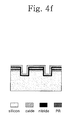
- FIGS. 4 a , 4 b , 4 c , 4 d , 4 e , 4 f , 4 g , 4 h , 4 i show steps for fabrication of the pattern depicted in FIG. 3;
- FIG. 5 is a scanning electron microscopic photograph of a microbridge fabricated in accordance with a micromechanical system fabrication method according to the present invention.
- FIG. 6 illustrates a comb drive fabricated in accordance with a micromechanical system fabrication method according to the present invention.
- FIG. 2 a shows two equilateral triangles surrounded by the ⁇ 111 ⁇ planes.
- FIG. 2 b shows a cross sectional view taken along line A-A′ showing other ⁇ 111 ⁇ planes.
- FIG. 2 c shows a cross sectional view taken along line B-B′ showing remaining ⁇ 111 ⁇ planes.
- the ⁇ 111 ⁇ planes slant against a [111] normal direction of the (111) planes at an angle of ⁇ 19.47°.
- the ⁇ 111 ⁇ planes which have been left after the etching step slant against the direction [111] at the angle of ⁇ 19.47°.
- FIG. 3 is a plan view of a pattern fabricated in accordance with the micromechanical system fabrication method according to the present invention.
- FIGS. 4 a to 4 i are cross sectional views taken along line C-C′ in FIG. 3 and show pattern fabrication steps.
- FIG. 3 also shows the ⁇ 111 ⁇ planes of the (111) single crystalline silicon and their normal directions. Especially, dotted lines in FIG. 3 indicate normal directions of the ⁇ 111 ⁇ planes left after the wet etching step using an aqueous alkaline solution (see FIG. 4 i ).
- a buffer oxide layer, a nitride layer, and a mask oxide layer are formed on a (111) single crystalline silicon substrate as shown in FIG. 4 a.
- Photolithography etching process (FIG. 4 b ) is then carried out on the buffer oxide layer, nitride layer, and mask oxide layer. After patterning as shown in FIG. 4 c , the photoresist layer is removed (FIG. 4 d ).
- a reactive ion etching (RIE) process is carried out on the (111) silicon substrate (FIG. 4 e ).
- the etch is performed vertically on the silicon substrate as shown in FIG. 4 e and an etched depth can be readily adjusted within the range from a sub-micrometer up to 500 ⁇ m in the RIE process.
- the etched depth on the silicon substrate corresponds to a thickness of a microstructure itself that will be finally separated from the silicon substrate in the micromechanical system.
- the thickness of the microstructure itself separated from the silicon substrate can be easily controlled within the range from the sub-micrometer up to 500 ⁇ m in this micromechanical system.
- the thickness of the microstructures are determined through the above first RIE step, and then a passivation step of overlaying protective films of the nitride layer and oxide layer is carried out (FIG. 4 f ). Subsequently, an other RIE process is performed with respect to the nitride layer and oxide layer as shown in FIG. 4 g.
- the second RIE process is also vertically carried out on the (111) silicon substrate (FIG. 4 h ).
- the etch is also performed vertically on the silicon substrate as shown in FIG. 4 h , and the etched depth can be readily adjusted within the range from a sub-micrometer up to 500 ⁇ m in the RIE process.
- the etched depth shown in FIG. 4 h corresponds to the spacing between the silicon substrate and the microstructures that will be finally separated from the silicon substrate in this micromechanical system.
- the etched depth on the silicon substrate can be controlled by using the RIE technique, thereby easily adjusting the spacing between the silicon substrate and the microstructures separated from the silicon substrate within the range from the sub-micrometer up to 500 ⁇ m in the micromechanical system.
- a wet etching step is carried out using an aqueous alkaline solution (FIG. 4 i ).
- the microstructures are separated from the silicon substrate through this step, so this step can be defined as a release-etching step.
- this release-etching step using an aqueous alkaline solution the ⁇ 100 ⁇ planes and the ⁇ 110 ⁇ planes are selectively etched, but the ⁇ 111 ⁇ planes is not etched.
- the microstructures that have been formed with the (111) single crystalline silicon are not damaged during the release-etching step. More specifically, the etching process does not damage a bottom surface of the microstructure.
- the ⁇ 111 ⁇ planes of the silicon substrate, which are left after the release-etching step, are not rough as shown in FIG. 4 i .
- the ⁇ 111 ⁇ planes left after the release-etching step slant against the [111] direction at an angle of ⁇ 19.47°, but this does not influence the microstructures separated from the silicon substrate. Since the etch is vertically carried out in the first RIE step as shown in FIG. 4 e , the side surfaces of the microstructures are patterned to be vertical.
- Such selective release-etching process also has an advantage of allowing the microstructure to be readily separated from the silicon substrate without additional etched holes.
- FIG. 5 is a scanning electron microscopic photograph of a microbridge fabricated in accordance with the micromechanical system fabrication method according to the present invention.
- the microbridge shown in FIG. 5 is formed to be 55 ⁇ m in length, 20 ⁇ m in width, and 4 ⁇ m in thickness.
- the spacing between the microbridge and the silicon substrate is 2 ⁇ m.
- the microbridge shown in FIG. 5 is formed by carrying out the RIE process on the (111) single crystalline silicon, so the side surfaces of the micro bridge are formed to be vertical.
- FIG. 6 illustrates a comb drive fabricated in accordance with the micromechanical system fabrication method.
- a moving beam in the form of tooth of a comb moves between tooth of a stationary beam that is also made in the form of tooth of a comb.
- Such movement of the moving beam causes change of spacing between the moving beam and the stationary beam.
- change of capacitance of a plate capacitor composed of the moving and stationary beams can be sensed.
- the side surfaces of microstructures such as the moving parts or the stationary parts can be formed to be vertical by using the RIE technique.
- the microstructures can be readily separated from the silicon substrate by employing the selective release-etching technique using slow etching ⁇ 111 ⁇ planes as the etch stop in an aqueous alkaline solution.
- the etched depth can be arbitrarily defined during the RIE step, thereby arbitrarily defining the thickness of the microstructures and the spacing between the microstructures and the silicon substrate.
Abstract
Description
Claims (23)
Priority Applications (1)
| Application Number | Priority Date | Filing Date | Title |
|---|---|---|---|
| US09/715,446 US6689694B1 (en) | 1998-04-01 | 2000-11-17 | Micromechanical system fabrication method using (111) single crystalline silicon |
Applications Claiming Priority (4)
| Application Number | Priority Date | Filing Date | Title |
|---|---|---|---|
| KR1019980011519A KR100300002B1 (en) | 1998-04-01 | 1998-04-01 | Micromachining method using single crystal silicon |
| KR98-11519 | 1998-04-01 | ||
| US09/250,519 US6150275A (en) | 1998-04-01 | 1999-02-16 | Micromechanical system fabrication method using (111) single crystalline silicon |
| US09/715,446 US6689694B1 (en) | 1998-04-01 | 2000-11-17 | Micromechanical system fabrication method using (111) single crystalline silicon |
Related Parent Applications (1)
| Application Number | Title | Priority Date | Filing Date |
|---|---|---|---|
| US09/250,519 Continuation US6150275A (en) | 1998-04-01 | 1999-02-16 | Micromechanical system fabrication method using (111) single crystalline silicon |
Publications (1)
| Publication Number | Publication Date |
|---|---|
| US6689694B1 true US6689694B1 (en) | 2004-02-10 |
Family
ID=30772278
Family Applications (1)
| Application Number | Title | Priority Date | Filing Date |
|---|---|---|---|
| US09/715,446 Expired - Lifetime US6689694B1 (en) | 1998-04-01 | 2000-11-17 | Micromechanical system fabrication method using (111) single crystalline silicon |
Country Status (1)
| Country | Link |
|---|---|
| US (1) | US6689694B1 (en) |
Cited By (5)
| Publication number | Priority date | Publication date | Assignee | Title |
|---|---|---|---|---|
| US20030049878A1 (en) * | 2000-04-11 | 2003-03-13 | Michael Offenberg | Micromechanical component and corresponding production method |
| US20040232502A1 (en) * | 2003-05-06 | 2004-11-25 | Walsin Lihwa Corporation | High-aspect-ratio-microstructure (HARM) |
| US20050070059A1 (en) * | 2001-12-04 | 2005-03-31 | Blakers Andrew William | Method of making thin silicon sheets for solar cells |
| WO2013023446A1 (en) * | 2011-08-12 | 2013-02-21 | 上海先进半导体制造股份有限公司 | Cavity manufacturing method |
| WO2015104086A1 (en) * | 2014-01-13 | 2015-07-16 | Robert Bosch Gmbh | Production method for a micromechanical part, and micromechanical part |
Citations (10)
| Publication number | Priority date | Publication date | Assignee | Title |
|---|---|---|---|---|
| US5195371A (en) | 1988-01-13 | 1993-03-23 | The Charles Stark Draper Laboratory, Inc. | Semiconductor chip transducer |
| US5594172A (en) | 1989-06-21 | 1997-01-14 | Nissan Motor Co., Ltd. | Semiconductor accelerometer having a cantilevered beam with a triangular or pentagonal cross section |
| US5725785A (en) | 1995-02-23 | 1998-03-10 | Kabushiki Kaisha Tokai Rika Denki Seisakusho | Method for manufacturing accelerometer sensor |
| US5883012A (en) | 1995-12-21 | 1999-03-16 | Motorola, Inc. | Method of etching a trench into a semiconductor substrate |
| US5882532A (en) | 1996-05-31 | 1999-03-16 | Hewlett-Packard Company | Fabrication of single-crystal silicon structures using sacrificial-layer wafer bonding |
| US5952572A (en) | 1996-01-19 | 1999-09-14 | Matsushita Electric Industrial Co., Ltd. | Angular rate sensor and acceleration sensor |
| US5962784A (en) | 1997-05-27 | 1999-10-05 | Alliedsignal Inc. | Micromachined rate and acceleration sensor |
| US5966066A (en) | 1994-06-10 | 1999-10-12 | Case Western Reserve University | Micromechanical memory sensor |
| US6020272A (en) | 1998-10-08 | 2000-02-01 | Sandia Corporation | Method for forming suspended micromechanical structures |
| US6150275A (en) * | 1998-04-01 | 2000-11-21 | Cho; Dong-Il | Micromechanical system fabrication method using (111) single crystalline silicon |
-
2000
- 2000-11-17 US US09/715,446 patent/US6689694B1/en not_active Expired - Lifetime
Patent Citations (10)
| Publication number | Priority date | Publication date | Assignee | Title |
|---|---|---|---|---|
| US5195371A (en) | 1988-01-13 | 1993-03-23 | The Charles Stark Draper Laboratory, Inc. | Semiconductor chip transducer |
| US5594172A (en) | 1989-06-21 | 1997-01-14 | Nissan Motor Co., Ltd. | Semiconductor accelerometer having a cantilevered beam with a triangular or pentagonal cross section |
| US5966066A (en) | 1994-06-10 | 1999-10-12 | Case Western Reserve University | Micromechanical memory sensor |
| US5725785A (en) | 1995-02-23 | 1998-03-10 | Kabushiki Kaisha Tokai Rika Denki Seisakusho | Method for manufacturing accelerometer sensor |
| US5883012A (en) | 1995-12-21 | 1999-03-16 | Motorola, Inc. | Method of etching a trench into a semiconductor substrate |
| US5952572A (en) | 1996-01-19 | 1999-09-14 | Matsushita Electric Industrial Co., Ltd. | Angular rate sensor and acceleration sensor |
| US5882532A (en) | 1996-05-31 | 1999-03-16 | Hewlett-Packard Company | Fabrication of single-crystal silicon structures using sacrificial-layer wafer bonding |
| US5962784A (en) | 1997-05-27 | 1999-10-05 | Alliedsignal Inc. | Micromachined rate and acceleration sensor |
| US6150275A (en) * | 1998-04-01 | 2000-11-21 | Cho; Dong-Il | Micromechanical system fabrication method using (111) single crystalline silicon |
| US6020272A (en) | 1998-10-08 | 2000-02-01 | Sandia Corporation | Method for forming suspended micromechanical structures |
Non-Patent Citations (6)
| Title |
|---|
| Bruce C. S. Chou, et al., "Anisotropic Etching of (111)-Oriented Silicon Applications," Part of the SPIE Conference on Micromachining and Microfabrication Process Technology IV, Santa Clara, California, SPIE, vol. 3511, pp. 337-341, Sep. 1998. |
| Graham Ensell, "Free Standing Single-Crystal Silicon Microstructures," J. Micromech, Microeng. 5, pp. 1-4, 1995. |
| J. G. Fleming, "Combining the Best of Bulk and Surface Micromachining Using Si (111) Substrates," Part of the SPIE Conference on Micromachining and Microfabrication Process Technology IV Santa Clara, California, SPIE, vol. 3511, pp. 162-168, Sep. 1998. |
| Sangwoo Lee, et al., "A New Micromachining Technology Using (111) Silicon," Digest of Papers Microprocesses and Nanotechnology '98, 1998 International Microprocesses and Nanotechnology Conference, Kyungju, Korea, pp. 174-175, Jul. 13-16, 1998. |
| Wolf et al. Silicon Processing For The VLSI Era Vol. 1: Process Technology, Lattice Press, Sunset Beach, A, USA, pp. 555, 1986. |
| Wolf et al., Silicon Processing for the VLSI Era, vol. 1: Process Technology, Lattice Press, Sunset Beach, CA, USA, pp. 1-5, 1986.* * |
Cited By (10)
| Publication number | Priority date | Publication date | Assignee | Title |
|---|---|---|---|---|
| US20030049878A1 (en) * | 2000-04-11 | 2003-03-13 | Michael Offenberg | Micromechanical component and corresponding production method |
| US7259436B2 (en) * | 2000-04-11 | 2007-08-21 | Robert Bosch Gmbh | Micromechanical component and corresponding production method |
| US20050070059A1 (en) * | 2001-12-04 | 2005-03-31 | Blakers Andrew William | Method of making thin silicon sheets for solar cells |
| US7169669B2 (en) * | 2001-12-04 | 2007-01-30 | Origin Energy Solar Pty. Ltd. | Method of making thin silicon sheets for solar cells |
| US20040232502A1 (en) * | 2003-05-06 | 2004-11-25 | Walsin Lihwa Corporation | High-aspect-ratio-microstructure (HARM) |
| US7088030B2 (en) * | 2003-05-06 | 2006-08-08 | Walsin Lihwa Corporation | High-aspect-ratio-microstructure (HARM) |
| WO2013023446A1 (en) * | 2011-08-12 | 2013-02-21 | 上海先进半导体制造股份有限公司 | Cavity manufacturing method |
| WO2015104086A1 (en) * | 2014-01-13 | 2015-07-16 | Robert Bosch Gmbh | Production method for a micromechanical part, and micromechanical part |
| CN105939958A (en) * | 2014-01-13 | 2016-09-14 | 罗伯特·博世有限公司 | Production method for a micromechanical part, and micromechanical part |
| CN105939958B (en) * | 2014-01-13 | 2018-09-21 | 罗伯特·博世有限公司 | Manufacturing method and micro-mechanical component for micro-mechanical component |
Similar Documents
| Publication | Publication Date | Title |
|---|---|---|
| US6150275A (en) | Micromechanical system fabrication method using (111) single crystalline silicon | |
| US5883012A (en) | Method of etching a trench into a semiconductor substrate | |
| US6428713B1 (en) | MEMS sensor structure and microfabrication process therefor | |
| EP0683921B1 (en) | Microstructures and single mask, single-crystal process for fabrication thereof | |
| US6582985B2 (en) | SOI/glass process for forming thin silicon micromachined structures | |
| US6379989B1 (en) | Process for manufacture of microoptomechanical structures | |
| US8828243B2 (en) | Scanning probe having integrated silicon tip with cantilever | |
| US20040121564A1 (en) | Method of forming semiconductor devices through epitaxy | |
| US20060278942A1 (en) | Antistiction MEMS substrate and method of manufacture | |
| US6694504B2 (en) | Method of fabricating an electrostatic vertical and torsional actuator using one single-crystalline silicon wafer | |
| EP0990195B1 (en) | Low-cost photoplastic cantilever | |
| US6756247B1 (en) | Integrated large area microstructures and micromechanical devices | |
| EP1062685A1 (en) | Integrated large area microstructures and micromechanical devices | |
| EP1582499A2 (en) | Encapsulation wafer process | |
| US6689694B1 (en) | Micromechanical system fabrication method using (111) single crystalline silicon | |
| US6187607B1 (en) | Manufacturing method for micromechanical component | |
| US20010009777A1 (en) | Method of etching a wafer layer using a sacrificial wall and structure formed thereby | |
| KR100732698B1 (en) | A method for fabricating a micro structures with multi thickness | |
| US6086774A (en) | Method of making released micromachined structures by directional etching | |
| US20020195417A1 (en) | Wet and dry etching process on <110> silicon and resulting structures | |
| US6790699B2 (en) | Method for manufacturing a semiconductor device | |
| EP1532637B1 (en) | Method of forming atomic force microscope tips | |
| Ayazi et al. | High aspect-ratio polysilicon micromachining technology | |
| EP1857407A2 (en) | Method of aligning mask layers to buried features | |
| US11731871B2 (en) | Actuator layer patterning with polysilicon and etch stop layer |
Legal Events
| Date | Code | Title | Description |
|---|---|---|---|
| AS | Assignment |
Owner name: CHO, DONG-IL, KOREA, REPUBLIC OF Free format text: ASSIGNMENT OF ASSIGNORS INTEREST;ASSIGNORS:LEE, SANGWOO;PARK, SANGJUN;REEL/FRAME:011328/0911 Effective date: 19991212 |
|
| AS | Assignment |
Owner name: CHROMUX TECHNOLOGIES, INC., CALIFORNIA Free format text: ASSIGNMENT OF ASSIGNORS INTEREST;ASSIGNOR:CHO, DONG-IL;REEL/FRAME:013975/0451 Effective date: 20030401 |
|
| AS | Assignment |
Owner name: CHO, DONG-II, KOREA, REPUBLIC OF Free format text: ASSIGNMENT OF ASSIGNORS INTEREST;ASSIGNOR:CHROMUX TECHNOLOGIES, INC.;REEL/FRAME:013998/0007 Effective date: 20030905 |
|
| STCF | Information on status: patent grant |
Free format text: PATENTED CASE |
|
| AS | Assignment |
Owner name: MICROMECHA, INC., JAPAN Free format text: ASSIGNMENT OF ASSIGNORS INTEREST;ASSIGNOR:CHO, DONG-IL;REEL/FRAME:015953/0545 Effective date: 20050321 |
|
| AS | Assignment |
Owner name: MICROMECHA, INC., KOREA, REPUBLIC OF Free format text: CORRECTED ASSIGNMENT TO CORRECT THE ASSIGNEE ADDRESS ON COVER SHEET PREVIOUSLY RECORDED AT REEL 015953 FRAME 0545;ASSIGNOR:CHO, DONG-IL;REEL/FRAME:016522/0706 Effective date: 20050321 |
|
| FPAY | Fee payment |
Year of fee payment: 4 |
|
| AS | Assignment |
Owner name: BARUN ELECTRONICS CO., LTD., KOREA, REPUBLIC OF Free format text: LICENSE;ASSIGNOR:MICROMECHA, INC.;REEL/FRAME:023304/0173 Effective date: 20090922 |
|
| FPAY | Fee payment |
Year of fee payment: 8 |
|
| AS | Assignment |
Owner name: BARUN ELECTRONICS CO., LTD., KOREA, REPUBLIC OF Free format text: CANCELLATION OF LICENSE AGREEMENT;ASSIGNOR:MICROMECHA, INC.;REEL/FRAME:031377/0459 Effective date: 20130930 |
|
| FPAY | Fee payment |
Year of fee payment: 12 |