US6717475B2 - Fast-acquisition phase-locked loop - Google Patents
Fast-acquisition phase-locked loop Download PDFInfo
- Publication number
- US6717475B2 US6717475B2 US10/032,848 US3284801A US6717475B2 US 6717475 B2 US6717475 B2 US 6717475B2 US 3284801 A US3284801 A US 3284801A US 6717475 B2 US6717475 B2 US 6717475B2
- Authority
- US
- United States
- Prior art keywords
- vco
- pll
- voltage
- charge
- time
- Prior art date
- Legal status (The legal status is an assumption and is not a legal conclusion. Google has not performed a legal analysis and makes no representation as to the accuracy of the status listed.)
- Expired - Lifetime, expires
Links
Images


Classifications
-
- H—ELECTRICITY
- H03—ELECTRONIC CIRCUITRY
- H03L—AUTOMATIC CONTROL, STARTING, SYNCHRONISATION, OR STABILISATION OF GENERATORS OF ELECTRONIC OSCILLATIONS OR PULSES
- H03L7/00—Automatic control of frequency or phase; Synchronisation
- H03L7/06—Automatic control of frequency or phase; Synchronisation using a reference signal applied to a frequency- or phase-locked loop
- H03L7/08—Details of the phase-locked loop
- H03L7/0802—Details of the phase-locked loop the loop being adapted for reducing power consumption
-
- H—ELECTRICITY
- H03—ELECTRONIC CIRCUITRY
- H03L—AUTOMATIC CONTROL, STARTING, SYNCHRONISATION, OR STABILISATION OF GENERATORS OF ELECTRONIC OSCILLATIONS OR PULSES
- H03L7/00—Automatic control of frequency or phase; Synchronisation
- H03L7/06—Automatic control of frequency or phase; Synchronisation using a reference signal applied to a frequency- or phase-locked loop
- H03L7/08—Details of the phase-locked loop
- H03L7/085—Details of the phase-locked loop concerning mainly the frequency- or phase-detection arrangement including the filtering or amplification of its output signal
- H03L7/089—Details of the phase-locked loop concerning mainly the frequency- or phase-detection arrangement including the filtering or amplification of its output signal the phase or frequency detector generating up-down pulses
- H03L7/0891—Details of the phase-locked loop concerning mainly the frequency- or phase-detection arrangement including the filtering or amplification of its output signal the phase or frequency detector generating up-down pulses the up-down pulses controlling source and sink current generators, e.g. a charge pump
-
- H—ELECTRICITY
- H03—ELECTRONIC CIRCUITRY
- H03L—AUTOMATIC CONTROL, STARTING, SYNCHRONISATION, OR STABILISATION OF GENERATORS OF ELECTRONIC OSCILLATIONS OR PULSES
- H03L7/00—Automatic control of frequency or phase; Synchronisation
- H03L7/06—Automatic control of frequency or phase; Synchronisation using a reference signal applied to a frequency- or phase-locked loop
- H03L7/08—Details of the phase-locked loop
- H03L7/10—Details of the phase-locked loop for assuring initial synchronisation or for broadening the capture range
- H03L7/101—Details of the phase-locked loop for assuring initial synchronisation or for broadening the capture range using an additional control signal to the controlled loop oscillator derived from a signal generated in the loop
- H03L7/102—Details of the phase-locked loop for assuring initial synchronisation or for broadening the capture range using an additional control signal to the controlled loop oscillator derived from a signal generated in the loop the additional signal being directly applied to the controlled loop oscillator
- H03L7/103—Details of the phase-locked loop for assuring initial synchronisation or for broadening the capture range using an additional control signal to the controlled loop oscillator derived from a signal generated in the loop the additional signal being directly applied to the controlled loop oscillator the additional signal being a digital signal
-
- H—ELECTRICITY
- H03—ELECTRONIC CIRCUITRY
- H03L—AUTOMATIC CONTROL, STARTING, SYNCHRONISATION, OR STABILISATION OF GENERATORS OF ELECTRONIC OSCILLATIONS OR PULSES
- H03L7/00—Automatic control of frequency or phase; Synchronisation
- H03L7/06—Automatic control of frequency or phase; Synchronisation using a reference signal applied to a frequency- or phase-locked loop
- H03L7/08—Details of the phase-locked loop
- H03L7/14—Details of the phase-locked loop for assuring constant frequency when supply or correction voltages fail or are interrupted
-
- H—ELECTRICITY
- H03—ELECTRONIC CIRCUITRY
- H03L—AUTOMATIC CONTROL, STARTING, SYNCHRONISATION, OR STABILISATION OF GENERATORS OF ELECTRONIC OSCILLATIONS OR PULSES
- H03L7/00—Automatic control of frequency or phase; Synchronisation
- H03L7/06—Automatic control of frequency or phase; Synchronisation using a reference signal applied to a frequency- or phase-locked loop
- H03L7/16—Indirect frequency synthesis, i.e. generating a desired one of a number of predetermined frequencies using a frequency- or phase-locked loop
- H03L7/18—Indirect frequency synthesis, i.e. generating a desired one of a number of predetermined frequencies using a frequency- or phase-locked loop using a frequency divider or counter in the loop
Definitions
- the invention relates to phase-locked loops (PLL's) and more particularly to compensating for variances in tuning voltage of a voltage-controlled oscillator (VCO) of a PLL during deactivated times of the PLL.
- PLL's phase-locked loops
- VCO voltage-controlled oscillator
- Portable telephones such as cellular telephones
- Portable telephones are very popular and becoming more popular and widespread every day. People enjoy the convenience of having a phone at their disposal no matter where they are. Impinging upon this convenience is the need to recharge the battery of the telephone periodically. If this time between recharges can be made longer, then the telephone becomes more convenient and useful.
- portable telephones sometimes are made to have an operating state called a paging mode.
- the phone periodically turns on the phone's receiver to check whether there is an incoming call.
- the phone is only on (activated) for a short period of time, and off (deactivated) for times between the on times, thus saving total average current and improving standby time (i.e., time when the phone is not in use).
- the fast-acquisition PLL may be broadly conceptualized as a system that compensates for VCO leakage current; thus reducing or eliminating frequency acquisition time.
- a fast-acquisition PLL that periodically activates and deactivates may utilize a system architecture that recognizes that VCO tuning voltage when the PLL is activated and the when PLL is locked (the VCO-lock voltage) is related to the lost charge while the PLL is deactivated.
- An implementation of the system architecture may include a charge pump, a loop filter connected to the charge pump, a VCO connected to the loop filter, a controller connected to the VCO, and a current source connected to the controller and the loop filter.
- the controller monitors a VCO tuning voltage at a VCO input and determines the amount of voltage lost during a deactivated time of the PLL, e.g., according to a difference between the VCO-lock voltage and the tuning voltage when the PLL is activated.
- the controller provides a signal to the current source indicating the lost voltage.
- the current source provides current to the loop filter to compensate for leakage current to help maintain the tuning voltage of the VCO at the VCO-lock voltage, or at least help ensure that the tuning voltage is approximately at the VCO-lock voltage when the PLL is activated.
- the current source may be several current sub-sources, such as current mirrors, that provide amounts of current that are related to each other, e.g., by a binary progression.
- the current sub-sources can be selected to provide appropriate amounts of current based on the signal from the controller.
- the current may be provided continuously throughout the deactivated time or may be provided during a portion of the deactivated time that is less than the entire deactivated time.
- fast-acquisition PLL may also utilize a system architecture that includes a charge pump, a loop filter connected to the charge pump, a VCO connected to the loop filter, and a controller connected to the VCO.
- the charge pump is responsive to the signal from the controller to turn on for at least a portion of the deactivated time of the PLL to provide sufficient charge to the VCO such that the tuning voltage when the PLL is activated is approximately at the VCO-lock voltage.
- the charge may be provided in one or more pulses and may be at an initial portion of the deactivated time of the PLL, or later.
- the controller can determine the lost charge from the VCO using techniques other than monitoring the VCO tuning voltage. For example, the controller can integrate charge provided to the loop filter by the charge pump during active time periods of the PLL. Alternatively, the controller can integrate an error signal provided by a phase detector of the PLL to the charge pump during active time periods of the PLL, e.g., from the time the PLL is activated until the PLL locks.
- FIG. 1 is a block diagram of a phase-locked loop system according to the invention.
- FIG. 2 is a block diagram of a current digital-to-analog converter shown in FIG. 1 .
- FIG. 3 is a graph of outputs of the converter shown in FIG. 2 .
- FIG. 4 is a graph of tuning voltage of a voltage-controlled oscillator shown in FIG. 1 in response to the outputs shown in FIG. 3 .
- FIG. 5 is a graph of an output of a charge pump shown in FIG. 1 .
- FIG. 6 is a graph of tuning voltage of the voltage-controlled oscillator shown in FIG. 1 in response to the outputs shown in FIG. 5 .
- FIG. 7 is a graph of an output of the charge pump shown in FIG. 1 .
- FIG. 8 is a graph of tuning voltage of the voltage-controlled oscillator shown in FIG. 1 in response to the output shown in FIG. 7 .
- FIG. 9 is a graph of outputs of the charge pump and a phase detector shown in FIG. 1 .
- FIG. 10 is a graph of a frequency difference between an output of the voltage-controlled oscillator shown in FIG. 1 and a frequency of a reference signal shown in FIG. 1 .
- FIG. 11 is a graph of tuning voltage of the voltage-controlled oscillator shown in FIG. 1 in response to the output of the charge pump shown in FIG. 9 .
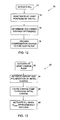
- FIG. 12 is a flowchart of a process of locking to a frequency using the system shown in FIG. 1 .
- FIG. 13 is a flowchart of initially compensating tuning voltage of the voltage-controlled oscillator shown in FIG. 1 .
- a phase-locked loop (PLL) 10 includes a synthesizer 12 , a loop filter 14 , and a voltage-controlled oscillator (VCO) 16 .
- the PLL 10 is configured to lock onto a reference frequency provided to the synthesizer 12 and output a signal of the same frequency from the VCO 16 .
- This output signal is provided by the VCO 16 in response to a tuning voltage provided at a tuning pin or tuning line 18 of the VCO 16 .
- the voltage provided to the tuning pin 18 is provided from the loop filter 14 .
- the loop filter 14 is a low-pass filter (LPF) that can be capacative in nature.
- LPF low-pass filter
- leakage current may flow from the synthesizer 12 (in particular, a charge pump 24 of the synthesizer 12 ), the loop filter 14 , and/or the VCO 16 .
- Leakage current may flow into the loop filter 14 from the charge pump 24 or from the charge pump 24 into the loop filter 14 .
- Leakage current from the loop filter 14 causes the tuning voltage at the tuning pin 18 to decrease during deactivated times of the PLL 10 and leakage current into the loop filter 14 acts to increase the tuning voltage at the tuning pin 18 .
- the synthesizer 12 is configured to, during active times of the PLL 10 , adjust the tuning voltage of the VCO 16 depending on a phase difference between the frequency of the VCO's output divided by N (of an N-counter described below) and the frequency of a reference signal.
- the synthesizer 12 is configured to adjust the tuning voltage until the output signal from the VCO 16 has approximately the same frequency as the frequency of the reference signal.
- the PLL 10 is considered to be locked to the reference frequency, with the tuning voltage at the tuning pin 18 being at a VCO-lock voltage.
- the VCO-lock voltage may be a range of voltages over which a frequency difference between the VCO output voltage signal and the reference signal REF is within an acceptable tolerance. This tolerance may be, for example, 100 Hz and the VCO sensitivity may be, for example, 45 MHz/volt.
- the synthesizer 12 includes control logic 20 , a circuit 22 , and a charge pump 24 .
- the circuit 22 includes a reference divider 23 , a pre-scalar 25 , and a phase detector 27 .
- the control logic 20 is configured to provide control signals to the charge pump 24 to regulate the amount and polarity of charge provided by the charge pump 24 .
- the charge pump 24 is configured to receive control signals from the control logic 20 and an error signal from the phase detector 27 , and in response to these signals, to provide charge to the loop filter 14 . The amount of time and polarity of the charge are determined by the control signals and the error signal.
- the charge from the charge pump 24 in filtered form, will be received by the VCO 16 and will affect the VCO tuning voltage, and therefore the output frequency of the output signal of the VCO 16 .
- the pre-scalar 25 is configured to receive a portion of the VCO output signal, scale the received signal portion, and pass a scaled signal to an N-counter of the reference divider 23 .
- the N-counter can divide the frequency of the scaled signal by N and provide the result 31 (f scal /N) to the phase detector 27 .
- An R-counter of the reference divider 23 can receive a reference signal REF, divide the REF signal by R and provide the divided signal 33 (REF/R) to the phase detector 27 .
- the phase detector 27 is configured to compare the signals from the R-divider and the N-divider and provide an error signal to the charge pump 24 indicative of the difference in frequencies of the R-divided and N-divided signals.
- the synthesizer 12 further includes a current digital-to-analog converter (DAC) 26 and an analog-to-digital converter (A/D) and control 28 .
- DAC current digital-to-analog converter
- A/D analog-to-digital converter
- These components 26 and 28 are configured to adjust the VCO tuning voltage while the PLL 10 is deactivated in response to, among other things, control signals from the control logic 20 .
- the A/D and control 28 is coupled to the tuning pin 18 and is configured to, in response to signals from the control logic 20 , monitor the tuning voltage.
- the monitored voltage includes the tuning voltage when the PLL 10 is initially activated (i.e., at the activation time t ac ) and when the PLL 10 is locked (i.e., the VCO-lock voltage).
- the A/D and control 28 is configured to, in response to signals from the control logic 20 , determine the difference between the VCO tuning voltage at the activation time t ac and the VCO-lock voltage. In response to this determination, the A/D and control 28 may output an indication of this difference to the current DAC 26 . In response to receiving the output from the A/D and control 28 , and receiving control signals from the control logic 20 , the current DAC 26 may supply a compensation current to the loop filter 14 . To supply the compensation current, the DAC 26 may be an adjustable current source that is responsive to the output from the A/D and control 28 , or may be multiple selectable current sources configured to be selected in response to the output from A/D and control 28 .
- the illustrated DAC 26 includes, here, a selector 30 , and three current mirrors 32 , 34 , and 36 , although other quantities of current mirrors may be employed.
- the selector 30 is coupled to the A/D and control 28 and configured to receive the output of the A/D and control 28 .
- the selector 30 is coupled to the control logic 20 (FIG. 1) and is configured to send and receive signals to and from the control logic 20 .
- the selector 30 can send indications of the output received from the A/D and control 28 to the control logic 20 and receive control signals from the control logic 20 indicative of which one or ones of the current mirrors 32 , 34 , and 36 to select.
- the selector 30 may select one or more of the current mirrors 32 , 34 , and 36 to provide any desired amounts of current.
- the one or more selected current mirrors 32 , 34 , and 36 each provide fixed amounts of current onto a common output line 38 , with currents from the mirrors, 32 , 34 , and 36 adding to form a single current on the output line 38 .
- the fixed amounts of the currents from the mirrors 32 , 34 , and 36 are preferably of differing amounts, here being a binary progression of current amplitudes with the current mirror 32 providing X amps of current, the current mirror 34 providing two times the number amps of the current mirror 32 (i.e., 2 ⁇ amps), and the current mirror 36 providing four times the amount of amps of the current mirror 32 (i.e., 4 ⁇ amps).
- the output line 38 is coupled to the loop filter 14 to provide the current from the current sources 32 , 34 , and 36 to the loop filter 14 to compensate for leakage current from the loop filter 14 during deactivated times of the PLL 10 (FIG. 1 ).
- the maximum and minimum current amounts providable by the current DAC 26 are determined to help ensure rapid locking of the PLL 10 .
- the maximum amount of current providable by the current mirrors 32 , 34 , and 36 corresponds to the expected maximum possible leakage current that might affect the tuning voltage.
- the smallest increment of current, here X amps, is selected to be less than an amount of current that would swing the VCO output signal from one extreme of the PLL's desired frequency tolerance to the other extreme. In other words, the smallest increment of current provided by the current DAC 26 is such that the total current will be able to adjust the VCO output signal to within the PLL's frequency tolerance.
- a process 70 of locking to a frequency with reduced acquisition times begins at stage 72 with the activation of the PLL 10 .
- Components of the PLL 10 are activated so that the PLL 10 may attempt to lock to a frequency of an incoming signal.
- the PLL 10 locks onto a reference frequency by adjusting the VCO tuning voltage until a frequency difference between the VCO output signal and the reference signal REF is within a selected frequency-difference tolerance, e.g. 100 Hz.
- the tolerance is the range in which the VCO is considered locked and can depend on the type of system in which the VCO resides.
- the circuit 22 determines the phase difference between the reference signal REF and the VCO output signal and provides an error signal indicating this difference to the charge pump 24 .
- This difference is proportional to the amount of time that the charge pump 24 is activated and to the polarity of the charge provided during this time by the charge pump 24 to the loop filter 14 .
- the loop filter 14 filters the charge from the charge pump 24 and provides the filtered charge to the tuning pin 18 of the VCO 16 .
- the VCO tuning voltage moves up or down, depending on the polarity and amount of the charge provided, and correspondingly provides a different frequency output, with the frequency increasing or decreasing depending on whether the VCO tuning voltage increased or decreased.
- the tuning voltage is adjusted until the phase difference detected by the circuit 22 is within a selected tolerance such that the frequency difference between the VCO output signal and the reference signal REF is within the selected frequency-difference tolerance.
- the PLL 10 is considered to be locked, with the VCO tuning voltage being within a VCO-lock voltage tolerance range.
- the VCO 16 can continue to refine its output frequency within the frequency tolerance, with the VCO tuning voltage approaching and possibly equaling a VCO-lock voltage at or near the center of the VCO-lock voltage tolerance range.
- the time from the activation time t ac , to the time when the PLL 10 is locked is referred to as the acquisition time t acquisition (FIG. 4) of the PLL 10 .
- the PLL 10 is deactivated some time later at a deactivation time t deac .
- At stage 74 at least some of the components of the PLL 10 used for locking to a frequency, are deactivated at the deactivation time t deac . While these PLL components are deactivated, absent compensating charge being provided to the VCO 16 , the VCO tuning voltage will drop, e.g., due to leakage current of the charge pump 24 , loop filter 14 , and/or the VCO 16 .
- the PLL 10 will experience some acquisition time to adjust the VCO tuning voltage such that VCO output signal and the reference signal REF are within the desired tolerance of each other. For example, if the PLL 10 is used as part of a cellular phone, and the cellular phone is in a paging mode in which the cellular phone periodically turns on and off (e.g., in an attempt to conserve battery time during stand-by) the PLL may experience repeated acquisition times.
- the acquisition time can be reduced or eliminated.
- the savings in time and energy for acquisition or re-acquisition of the proper VCO output signal more than compensates for the added energy to put the VCO tuning voltage at or near the VCO-lock voltage at the activation time t ac .
- the A/D and control 28 monitors the VCO tuning voltage and determines compensation current to be supplied to the loop filter 14 during deactivated times of the PLL 10 . This may be an interactive process with the compensation determined by putting the VCO tuning voltage closer to the VCO-lock voltage (or some other voltage) each iteration until a limit and/or an acceptable proximity is reached.
- the A/D and control 28 determines the difference between the tuning voltage at or near the activation time t ac and the VCO-lock voltage. To do this, the A/D and control 28 monitors the VCO tuning voltage at a time when the VCO tuning voltage is at a voltage VCO-lock 1 , e.g., a time t 1 , and at a time at or near the activation time t ac of the PLL 10 , e.g., t 2 . Alternatively, if the relationship between the voltage at or near time t ac and the voltage at another time between t deac and t ac is known, the voltage at this other time can be monitored.
- the A/D and control 28 determines the VCO-lock voltage VCO-lock 1 , and, as indicated by plot 40 in FIG. 4, at time t 2 , the A/D control 28 determines the VCO tuning voltage in the absence of any compensating current supplied to the loop filter 14 . By comparing these two voltages, the A/D and control 28 determines the amount of compensation current to be supplied to the loop filter 14 such that the VCO tuning voltage is at or near the VCO lock voltage VCO-lock 1 at the activation time t ac .
- the A/D and control 28 controls the current DAC 26 to provide compensation charge in the form of a current at the DAC output to the loop filter 14 to help ensure that the VCO tuning voltage at the activation time t ac is at or near a desired VCO-lock voltage.
- the A/D and control 28 may determine that the compensation current should be equal to I 1 to have the VCO tuning voltage at or near the VCO-lock voltage VCO-lock 1 at the acquisition time t ac .
- the A/D and control 28 controls the current DAC 26 to output the compensation current I 1 continuously from the deactivation time t deac to the activation time t ac as shown by plot 42 in FIG. 3 .
- the VCO tuning voltage initially declines after the deactivation time t deac and eventually returns to the previous VCO lock voltage VCO-lock 1 in time for the next activation time t ac .
- the A/D and control 28 can also determine compensation currents if the desired VCO tuning voltage for the next activation t ac is different than the VCO tuning voltage from the previous active time of the PLL 10 .
- the A/D and control 28 can control the current DAC 26 to output a compensation current I 2 , that is greater than I 1 , during the deactivated time of the PLL 10 to affect the VCO tuning voltage as indicated by plot 46 in FIG. 4 .
- I 2 compensation current of I 2
- the VCO tuning voltage approximately equals a VCO-lock 2 voltage at the next activation time t ac .
- the A/D and control 28 can control the current DAC 26 to provide a compensation current I 3 , that is less than I 1 (and possibly opposite in polarity), during the deactivated time of the PLL 10 to adjust the VCO tuning voltage as shown in plot 48 of FIG. 4 .
- the current I 3 causes the VCO tuning voltage to approximately equal a voltage VCO-lock 3 at the activation time t ac .
- VCO tuning voltage may be adjusted during deactivated times of the PLL 10 such as providing charge from the charge pump 24 to the loop filter 14 .
- the current DAC 26 can be eliminated and the A/D and control 28 coupled to the charge pump 24 and configured to control charge pump 24 to provide compensating charge during deactivated times of the PLL 10 .
- the A/D and control 28 may be configured to actuate the charge pump 24 for times and amounts that will adjust the VCO tuning voltage as desired. In at least some embodiments, for example, assuming that the VCO tuning voltage is to be returned to a VCO lock voltage VCO-lock 4 (FIG.
- the A/D and control 28 causes the charge pump 24 to activate at the deactivation time t deac of PLL 10 to provide a pulse 50 of charge to the loop filter 14 .
- the pulse 50 causes a corresponding increase in the VCO tuning voltage, because the VCO 16 indirectly receives charge from the synthesizer 12 .
- the increase in VCO tuning voltage is indicated in plot 52 in FIG. 6 .
- the VCO tuning voltage again indicated by the plot 52 , decreases, e.g., due to leakage current of the loop filter 14 , the charge pump 24 , and/or the VCO 16 .
- the duration and polarization of pulse 50 are determined by the A/D and control 28 such that the VCO tuning voltage returns to approximately the VCO lock voltage VCO-lock 4 by the next activation time t ac .
- the pulse duration may typically be less than about 0.001% of the deactivated time.
- the pulse of charge provided by the charge pump 24 can be before an initial activation time of the PLL 10 .
- a capacitor 17 of a resonant circuit 19 of the VCO 16 may be completely, or nearly completely, depleted of charge.
- the deactivation steady state may exist, e.g., if the PLL 10 has been deactivated for a long time, as when a system using the PLL 10 is turned off and is not in standby mode (e.g., a paging mode of a cellular telephone).
- a process 80 of initially compensating the tuning voltage begins at stage 82 where the charge pump 24 is activated.
- indicia of the amount and polarization of initial charge to be provided by the charge pump 24 can be stored, e.g., in memory associated with (e.g., included in) the control logic 20 and retrieved by the control logic 20 in response to powering up of the charge pump 24 .
- the control logic 20 sends signals to the charge pump 24 causing the pump 24 to supply the appropriate amount and polarization of initial charge in a pulse 60 to the loop filter 14 before the initial activation time t ac of the PLL 10 .
- VCO tuning voltage This causes the VCO tuning voltage to reach the lock voltage VCO-LOCK, preferably, approximately at the activation time t ac , when, at stage 88 , the PLL 10 is activated. Further adjustment of the VCO tuning voltage could be accomplished as discussed above using the initial and locked voltages.
- Initial setting of the VCO tuning voltage may be accomplished, e.g., by not activating (i.e., delaying activation) of all components of the PLL 10 when the PLL 10 is initially powered up, while allowing the charge pump 24 and the control logic 20 to operate. It may be desirable to let counters in the system 10 run for at least one cycle before turning on the charge pump 24 to help avoid having a counter output reflect a frequency of the VCO while the loop filter 14 is charging. Such a counter output may undesirably affect the output of the charge pump 24 , and put the VCO out of tolerance temporarily.
- the pulse of charge provided by the charge pump 24 does not need to be at the initial portion of the deactivated time (between t deac and t ac ) of the PLL 10 .
- the A/D and control 28 can activate the charge pump 24 at other times or portions of the deactivated time of the PLL 10 to adjust the VCO tuning voltage.
- the VCO tuning voltage, as affected by the pulse 54 is shown in FIG. 6 by a plot 56 . Also, more than one pulse can be provided to the filter 14 by the pump 24 during the deactivated time.
- the VCO tuning voltage is to be set to a different VCO lock voltage, such as from VCO lock voltage VCO-lock 4 to a VCO lock voltage VCO-lock 5 , then different amounts of charge than those provided by pulses 50 or 54 can be provided by the charge pump 24 . Accordingly, the VCO lock voltage VCO-lock 5 is lower than it would be if no compensating charge or currents were provided to the loop filter 14 during the deactivated time of the PLL 10 .
- the A/D and control 28 controls the charge pump 24 to provide a pulse 58 that is opposite in polarity to the pulse 50 .
- the pulse 58 causes the VCO tuning voltage to decrease further than it would absent any compensation during the deactivated time of the PLL 10 .
- the pulse amount is determined such that is causes the VCO tuning voltage to be at approximately the VCO lock voltage VCO-lock 5 at the next activation time t ac .
- the VCO tuning voltage may differ from the VCO lock voltage VCO-lock by an amount ⁇ V as shown in FIG. 11 .
- the charge pump 24 provides charge to the loop filter 14 until the PLL is locked at a time t L , marking the end of the acquisition time t acquisition .
- FIG. 10 shows the corresponding difference in phase of the VCO output signal and the reference signal REF. After the lock time t L , as the phase begins to differ between the VCO output signal and the reference signal REF, the difference will eventually exceed an acceptable tolerance ⁇ to 1 in the phase difference.
- both the charge pump output and the error signal output by the phase detector are indicative of the amount by which the VCO tuning voltage differs from the VCO-lock voltage at the activation time t ac .
- the phase detector output or the charge pump output can be used to determine the amount of deactivated-time compensation to be employed.
- This compensation corresponds to the difference in VCO tuning voltage at the activation time t ac and the desired VCO-lock voltage.
- An indication of this difference can be determined by integrating the phase detector output or the charge pump output during the acquisition time t acquisition , during the acquisition time t acquisition plus some additional time to allow the VCO tuning voltage to approach, and possibly equal, the VCO-lock voltage, or during the entire active time between the activation time t ac and the deactivation time t deac .
- the integration may result in compensation that is slightly off of an ideal compensation if the VCO tuning voltage at the end time of the integration is not at the desired VCO lock voltage. This slight error, however, will likely be better than no compensation, and thus may still be useful.
- the A/D and control 28 can be configured to monitor the phase detector output or the charge pump output and to integrate the monitored output.
- the A/D and control 28 may be configured to use the integrated output to determine a digitized control signal for the charge pump 24 or, if used, the current DAC 26 .
- the indication determined by the A/D and control 28 can be based upon maintaining or returning the VCO tuning voltage to the prior VCO-lock voltage, or based on setting the VCO tuning voltage to a voltage that differs from the previous VCO-lock voltage.
- the digitized control signal can be, or can be added to or subtracted from, a count of a counter 35 in the charge pump 24 (or, e.g., in the A/D and control 28 ). The count represents the length of time that a reduced output of the charge pump 24 , or a separate charge pump, will provide charge to the loop filter 14 during the next deactivated time to properly compensate for charge lost by the loop filter 14 .
- the A/D and control 28 can have an output of one or more bits.
- a one-bit output could indicate a fixed adjustment amount, of charge for the loop filter 14 , of a polarity corresponding to the value of the bit. The total adjustment amount could vary depending on how long the charge pump 24 provides charge in response to the A/D and control output.
- a multi-bit output of the A/D and control 28 could indicate both the polarity and amount of charge to provide to the loop filter 14 .
- each output is a square pulse with a width proportional to the initial frequency difference of the VCO output signal and the reference signal REF.
- the phase detector may have a value of either 1 or ⁇ 1. Alternatively, this may be implemented with two digital signals having values of 0 or 1, with one signal indicating on/off of the charge pump 24 and the other signal indicating the polarity for the charge pump output.
Abstract
Description
Claims (34)
Priority Applications (2)
| Application Number | Priority Date | Filing Date | Title |
|---|---|---|---|
| US10/032,848 US6717475B2 (en) | 2001-11-01 | 2001-11-01 | Fast-acquisition phase-locked loop |
| US10/754,388 US6867655B2 (en) | 2001-11-01 | 2004-01-09 | Fast-acquisition phase-locked loop |
Applications Claiming Priority (1)
| Application Number | Priority Date | Filing Date | Title |
|---|---|---|---|
| US10/032,848 US6717475B2 (en) | 2001-11-01 | 2001-11-01 | Fast-acquisition phase-locked loop |
Related Child Applications (1)
| Application Number | Title | Priority Date | Filing Date |
|---|---|---|---|
| US10/754,388 Continuation US6867655B2 (en) | 2001-11-01 | 2004-01-09 | Fast-acquisition phase-locked loop |
Publications (2)
| Publication Number | Publication Date |
|---|---|
| US20030080818A1 US20030080818A1 (en) | 2003-05-01 |
| US6717475B2 true US6717475B2 (en) | 2004-04-06 |
Family
ID=21867142
Family Applications (2)
| Application Number | Title | Priority Date | Filing Date |
|---|---|---|---|
| US10/032,848 Expired - Lifetime US6717475B2 (en) | 2001-11-01 | 2001-11-01 | Fast-acquisition phase-locked loop |
| US10/754,388 Expired - Lifetime US6867655B2 (en) | 2001-11-01 | 2004-01-09 | Fast-acquisition phase-locked loop |
Family Applications After (1)
| Application Number | Title | Priority Date | Filing Date |
|---|---|---|---|
| US10/754,388 Expired - Lifetime US6867655B2 (en) | 2001-11-01 | 2004-01-09 | Fast-acquisition phase-locked loop |
Country Status (1)
| Country | Link |
|---|---|
| US (2) | US6717475B2 (en) |
Cited By (5)
| Publication number | Priority date | Publication date | Assignee | Title |
|---|---|---|---|---|
| US20050046493A1 (en) * | 2003-08-04 | 2005-03-03 | Karl Hofmann | Circuit and method for faster frequency switching in a phase locked loop |
| US20050174179A1 (en) * | 2002-05-28 | 2005-08-11 | Koninklijke Philips Electronics N.V. | Pll circuit |
| US20070188242A1 (en) * | 2006-02-15 | 2007-08-16 | Hynix Semiconductor Inc. | Phase locked loop for stably operating in a matter that is insensitive to variation in process, voltage and temperature and method of operating the same |
| US20110012792A1 (en) * | 2009-07-17 | 2011-01-20 | Motorola, Inc. | Antenna arrangement for multimode communication device |
| US8098788B1 (en) * | 2008-05-21 | 2012-01-17 | Maxim Integrated Products, Inc. | System and method for automatic leakage control circuit for clock/data recovery and charge-pump phase locked loops |
Families Citing this family (6)
| Publication number | Priority date | Publication date | Assignee | Title |
|---|---|---|---|---|
| US7386085B2 (en) * | 2002-05-30 | 2008-06-10 | Broadcom Corporation | Method and apparatus for high speed signal recovery |
| US7365582B1 (en) | 2003-05-14 | 2008-04-29 | Marvell International Ltd. | Bootstrapped charge pump driver in a phase-lock loop |
| JP4176705B2 (en) * | 2004-12-02 | 2008-11-05 | シャープ株式会社 | PLL circuit |
| GB0626024D0 (en) * | 2006-12-29 | 2007-02-07 | Nokia Corp | Dynamically adjusted phase locked loop |
| TWI382668B (en) * | 2009-09-07 | 2013-01-11 | Richwave Technology Corp | Phase lock loop and control method thereof |
| JP2011259331A (en) * | 2010-06-11 | 2011-12-22 | Panasonic Corp | Pll circuit |
Citations (3)
| Publication number | Priority date | Publication date | Assignee | Title |
|---|---|---|---|---|
| US5920233A (en) * | 1996-11-18 | 1999-07-06 | Peregrine Semiconductor Corp. | Phase locked loop including a sampling circuit for reducing spurious side bands |
| US6157271A (en) * | 1998-11-23 | 2000-12-05 | Motorola, Inc. | Rapid tuning, low distortion digital direct modulation phase locked loop and method therefor |
| US6466096B1 (en) * | 2001-05-22 | 2002-10-15 | Analog Devices, Inc. | Tunable oscillator with leakage compensation |
Family Cites Families (5)
| Publication number | Priority date | Publication date | Assignee | Title |
|---|---|---|---|---|
| US5334952A (en) * | 1993-03-29 | 1994-08-02 | Spectralink Corporation | Fast settling phase locked loop |
| US6046646A (en) * | 1997-06-13 | 2000-04-04 | Lo; Pedro W. | Modulation of a phase locked loop for spreading the spectrum of an output clock signal |
| US6064274A (en) * | 1998-10-30 | 2000-05-16 | Sony Corporation Of Japan | RCB cancellation in high-side low power supply current sources |
| FR2800939B1 (en) * | 1999-11-09 | 2002-01-25 | St Microelectronics Sa | DIGITAL LOOP WITH PHASE LOCK |
| US6509801B1 (en) * | 2001-06-29 | 2003-01-21 | Sierra Monolithics, Inc. | Multi-gigabit-per-sec clock recovery apparatus and method for optical communications |
-
2001
- 2001-11-01 US US10/032,848 patent/US6717475B2/en not_active Expired - Lifetime
-
2004
- 2004-01-09 US US10/754,388 patent/US6867655B2/en not_active Expired - Lifetime
Patent Citations (3)
| Publication number | Priority date | Publication date | Assignee | Title |
|---|---|---|---|---|
| US5920233A (en) * | 1996-11-18 | 1999-07-06 | Peregrine Semiconductor Corp. | Phase locked loop including a sampling circuit for reducing spurious side bands |
| US6157271A (en) * | 1998-11-23 | 2000-12-05 | Motorola, Inc. | Rapid tuning, low distortion digital direct modulation phase locked loop and method therefor |
| US6466096B1 (en) * | 2001-05-22 | 2002-10-15 | Analog Devices, Inc. | Tunable oscillator with leakage compensation |
Cited By (9)
| Publication number | Priority date | Publication date | Assignee | Title |
|---|---|---|---|---|
| US20050174179A1 (en) * | 2002-05-28 | 2005-08-11 | Koninklijke Philips Electronics N.V. | Pll circuit |
| US7116177B2 (en) * | 2002-05-28 | 2006-10-03 | Koninklijke Philips Electronics N.V. | PLL circuit leakage compensation circuit for generating a leakage compensation signal |
| US20050046493A1 (en) * | 2003-08-04 | 2005-03-03 | Karl Hofmann | Circuit and method for faster frequency switching in a phase locked loop |
| US7129791B2 (en) * | 2003-08-04 | 2006-10-31 | Atmel Germany Gmbh | Circuit and method for faster frequency switching in a phase locked loop |
| US20070188242A1 (en) * | 2006-02-15 | 2007-08-16 | Hynix Semiconductor Inc. | Phase locked loop for stably operating in a matter that is insensitive to variation in process, voltage and temperature and method of operating the same |
| US7443249B2 (en) * | 2006-02-15 | 2008-10-28 | Hynix Semiconductor Inc. | Phase locked loop for stably operating in a matter that is insensitive to variation in process, voltage and temperature and method of operating the same |
| US20090033429A1 (en) * | 2006-02-15 | 2009-02-05 | Hynix Semiconductor, Inc. | Phase locked loop for stably operating in a matter that is insensitive to variation in process, voltage and temperature and method of operating the same |
| US8098788B1 (en) * | 2008-05-21 | 2012-01-17 | Maxim Integrated Products, Inc. | System and method for automatic leakage control circuit for clock/data recovery and charge-pump phase locked loops |
| US20110012792A1 (en) * | 2009-07-17 | 2011-01-20 | Motorola, Inc. | Antenna arrangement for multimode communication device |
Also Published As
| Publication number | Publication date |
|---|---|
| US20040142671A1 (en) | 2004-07-22 |
| US6867655B2 (en) | 2005-03-15 |
| US20030080818A1 (en) | 2003-05-01 |
Similar Documents
| Publication | Publication Date | Title |
|---|---|---|
| US6806786B1 (en) | Phase-locked loop with self-selecting multi-band VCO | |
| AU729665B2 (en) | Method and apparatus for reducing standby current in communications equipment | |
| US6667642B1 (en) | Method and circuit for reducing the power up time of a phase lock loop | |
| US6717475B2 (en) | Fast-acquisition phase-locked loop | |
| US8073416B2 (en) | Method and apparatus for controlling a bias current of a VCO in a phase-locked loop | |
| EP0899637A1 (en) | Spacecraft disciplined reference oscillator | |
| EP0464139A4 (en) | Frequency synthesizer with control of start-up battery saving operations | |
| US7884657B2 (en) | Oscillation frequency control circuit | |
| US20040000956A1 (en) | Phase-locked loop with automatic frequency tuning | |
| WO2004075414B1 (en) | Circuitry to reduce pll lock acquisition time | |
| AU759155B2 (en) | Oscillator using calibration means | |
| EP2066035B1 (en) | Oscillation frequency control circuit | |
| JP4216075B2 (en) | Fractional N-Frequency Synthesizer using Fractional Compensation Method (Fractional-NFREQUENCYSYNTHESIZER) | |
| JP4355350B2 (en) | Oscillation frequency control circuit | |
| US6466069B1 (en) | Fast settling charge pump | |
| US20080191760A1 (en) | PLLS covering wide operating frequency ranges | |
| US8629728B2 (en) | VCO control circuit and method thereof, fast locking PLL and method for fast locking PLL | |
| US6411144B1 (en) | Phase-locked loop circuit | |
| US20070024381A1 (en) | Charge supply apparatus and method in frequency synthesizer | |
| US11303284B1 (en) | Low-power fractional analog PLL without feedback divider | |
| US6747521B1 (en) | Analog memory cell in a low power oscillator | |
| US6734748B2 (en) | Phase-locked loop oscillator with counter bypass | |
| US6278304B1 (en) | Look-ahead enabling charge pump in phase-locked loop circuits | |
| US20070241825A1 (en) | Phase Locked Loop Circuit | |
| US8432201B1 (en) | Phase-locked loop (PLL) circuit |
Legal Events
| Date | Code | Title | Description |
|---|---|---|---|
| AS | Assignment |
Owner name: CONEXANT SYSTEMS, INC., CALIFORNIA Free format text: ASSIGNMENT OF ASSIGNORS INTEREST;ASSIGNOR:MCCARTHY, EVAN S.;REEL/FRAME:012423/0826 Effective date: 20011024 |
|
| AS | Assignment |
Owner name: ALPHA INDUSTRIES, INC., MASSACHUSETTS Free format text: MERGER;ASSIGNOR:WASHINGTON SUB, INC.;REEL/FRAME:013180/0123 Effective date: 20020625 Owner name: SKYWORKS SOLUTIONS, INC., CALIFORNIA Free format text: MERGER;ASSIGNOR:ALPHA INDUSTRIES, INC.;REEL/FRAME:013180/0095 Effective date: 20020625 Owner name: WASHINGTON SUB, INC., CALIFORNIA Free format text: ASSIGNMENT OF ASSIGNORS INTEREST;ASSIGNOR:CONEXANT SYSTEMS, INC.;REEL/FRAME:013180/0082 Effective date: 20020625 |
|
| AS | Assignment |
Owner name: CONEXANT SYSTEMS, INC., CALIFORNIA Free format text: SECURITY INTEREST;ASSIGNOR:ALPHA INDUSTRIES, INC.;REEL/FRAME:013240/0860 Effective date: 20020625 |
|
| AS | Assignment |
Owner name: ALPHA INDUSTRIES, INC., MASSACHUSETTS Free format text: RELEASE AND RECONVEYANCE/SECURITY INTEREST;ASSIGNOR:CONEXANT SYSTEMS, INC.;REEL/FRAME:014580/0880 Effective date: 20030307 |
|
| STCF | Information on status: patent grant |
Free format text: PATENTED CASE |
|
| FEPP | Fee payment procedure |
Free format text: PAYOR NUMBER ASSIGNED (ORIGINAL EVENT CODE: ASPN); ENTITY STATUS OF PATENT OWNER: LARGE ENTITY |
|
| FPAY | Fee payment |
Year of fee payment: 4 |
|
| REMI | Maintenance fee reminder mailed | ||
| CC | Certificate of correction | ||
| FEPP | Fee payment procedure |
Free format text: PAYOR NUMBER ASSIGNED (ORIGINAL EVENT CODE: ASPN); ENTITY STATUS OF PATENT OWNER: LARGE ENTITY Free format text: PAYER NUMBER DE-ASSIGNED (ORIGINAL EVENT CODE: RMPN); ENTITY STATUS OF PATENT OWNER: LARGE ENTITY |
|
| FPAY | Fee payment |
Year of fee payment: 8 |
|
| FPAY | Fee payment |
Year of fee payment: 12 |