US6725114B1 - Method and apparatus for automatically generating schedules for wafer processing within a multichamber semiconductor wafer processing tool - Google Patents
Method and apparatus for automatically generating schedules for wafer processing within a multichamber semiconductor wafer processing tool Download PDFInfo
- Publication number
- US6725114B1 US6725114B1 US09/771,254 US77125401A US6725114B1 US 6725114 B1 US6725114 B1 US 6725114B1 US 77125401 A US77125401 A US 77125401A US 6725114 B1 US6725114 B1 US 6725114B1
- Authority
- US
- United States
- Prior art keywords
- overscore
- wafer
- vertex
- successor
- schedule
- Prior art date
- Legal status (The legal status is an assumption and is not a legal conclusion. Google has not performed a legal analysis and makes no representation as to the accuracy of the status listed.)
- Expired - Fee Related, expires
Links
Images


Classifications
-
- H—ELECTRICITY
- H01—ELECTRIC ELEMENTS
- H01L—SEMICONDUCTOR DEVICES NOT COVERED BY CLASS H10
- H01L21/00—Processes or apparatus adapted for the manufacture or treatment of semiconductor or solid state devices or of parts thereof
-
- H—ELECTRICITY
- H01—ELECTRIC ELEMENTS
- H01L—SEMICONDUCTOR DEVICES NOT COVERED BY CLASS H10
- H01L21/00—Processes or apparatus adapted for the manufacture or treatment of semiconductor or solid state devices or of parts thereof
- H01L21/67—Apparatus specially adapted for handling semiconductor or electric solid state devices during manufacture or treatment thereof; Apparatus specially adapted for handling wafers during manufacture or treatment of semiconductor or electric solid state devices or components ; Apparatus not specifically provided for elsewhere
- H01L21/67005—Apparatus not specifically provided for elsewhere
- H01L21/67242—Apparatus for monitoring, sorting or marking
- H01L21/67276—Production flow monitoring, e.g. for increasing throughput
-
- G—PHYSICS
- G03—PHOTOGRAPHY; CINEMATOGRAPHY; ANALOGOUS TECHNIQUES USING WAVES OTHER THAN OPTICAL WAVES; ELECTROGRAPHY; HOLOGRAPHY
- G03F—PHOTOMECHANICAL PRODUCTION OF TEXTURED OR PATTERNED SURFACES, e.g. FOR PRINTING, FOR PROCESSING OF SEMICONDUCTOR DEVICES; MATERIALS THEREFOR; ORIGINALS THEREFOR; APPARATUS SPECIALLY ADAPTED THEREFOR
- G03F7/00—Photomechanical, e.g. photolithographic, production of textured or patterned surfaces, e.g. printing surfaces; Materials therefor, e.g. comprising photoresists; Apparatus specially adapted therefor
- G03F7/70—Microphotolithographic exposure; Apparatus therefor
- G03F7/70483—Information management; Active and passive control; Testing; Wafer monitoring, e.g. pattern monitoring
- G03F7/70491—Information management, e.g. software; Active and passive control, e.g. details of controlling exposure processes or exposure tool monitoring processes
- G03F7/70533—Controlling abnormal operating mode, e.g. taking account of waiting time, decision to rework or rework flow
-
- Y—GENERAL TAGGING OF NEW TECHNOLOGICAL DEVELOPMENTS; GENERAL TAGGING OF CROSS-SECTIONAL TECHNOLOGIES SPANNING OVER SEVERAL SECTIONS OF THE IPC; TECHNICAL SUBJECTS COVERED BY FORMER USPC CROSS-REFERENCE ART COLLECTIONS [XRACs] AND DIGESTS
- Y10—TECHNICAL SUBJECTS COVERED BY FORMER USPC
- Y10S—TECHNICAL SUBJECTS COVERED BY FORMER USPC CROSS-REFERENCE ART COLLECTIONS [XRACs] AND DIGESTS
- Y10S438/00—Semiconductor device manufacturing: process
- Y10S438/907—Continuous processing
- Y10S438/908—Utilizing cluster apparatus
Definitions
- the present invention relates to a multiple chamber wafer processing tool and, more particularly, to a method and apparatus for automatically generating a schedule(s) for a semiconductor wafer within a multiple chamber semiconductor wafer processing tool.
- FIG. 1 depicts, in part, a schematic diagram of the Endura® System.
- the wafers 128 are typically carried from storage to the system in a plastic transport cassette 126 that is placed within one of the loadlock chambers 120 or 122 .
- the robotic transport mechanism 124 transports the wafers 128 , one at a time, from the cassette 126 to any of the three chambers 118 , 102 , or 114 .
- a given wafer is first placed in the wafer orienter/degas chamber 118 , then moved to the preclean chamber 114 .
- the cooldown chamber 102 is generally not used until after the wafer is processed within the process chambers 104 , 106 , 108 , 110 .
- Individual wafers are carried upon a wafer transport blade 130 that is located at the distal end of the first robotic mechanism 124 .
- the transport operation is controlled by a sequencer 136 .
- the transfer chamber 112 is surrounded by and has access to the four process chambers 104 , 106 , 108 and 110 as well as the preclean chamber 114 and the cooldown chamber 102 .
- the transfer chamber 112 contains a second robotic transport mechanism 132 .
- the mechanism 132 has a wafer transport blade 134 attached to its distal end for carrying the individual wafers.
- the wafer transport blade 134 of the second transport mechanism 132 retrieves a wafer from the preclean chamber 114 and carries that wafer to the first stage of processing, for example, a physical vapor deposition (PVD) stage within chamber 104 . Once the wafer is processed and the PVD stage deposits material upon the wafer, the wafer can then be moved to a second stage of processing and so on.
- PVD physical vapor deposition
- the transport mechanism 132 moves the wafer from the process chamber and transports the wafer to the cooldown chamber 102 .
- the wafer is then removed from the cooldown chamber using the first transport mechanism 124 within the buffer chamber 116 .
- the wafer is placed in the transport cassette 126 within the loadlock chamber 122 .
- a cluster tool may be coupled to a factory interface comprising at least one factory interface robot, one or more metrology chambers/defect control chambers and one or more load ports, and one or more wafer orienting chambers.
- the factory interface is coupled to the load locks of the cluster tool.
- a cluster tool contains n chambers, denoted by C 1 , C 2 , . . . , C n , one or more transfer chambers (robots) 112 and 116 , and one or more loadlocks 120 and 122 .
- the exact arrangement of chambers, robots and loadlocks is referred to as the “configuration” of the tool.
- a wafer W a to be processed is taken from a loadlock, placed successively into various chambers as each chamber performs a particular process upon the wafer.
- a wafer's trace is the trajectory of a particular wafer through the cluster tool; that is, a trace is the order in which chambers are visited by a wafer (not necessarily C i+1 after C i ). This should be distinguished from the term “processing sequence” which is the order of applying processes (recipes) to a wafer. If more than one chamber performs the same process (parallel chambers), a given processing sequence may be satisfied by several different traces.
- a wafer which completes its processing sequence and is returned to the loadlock is said to be processed by the tool.
- scheduling routine A routine which schedules the movement of wafers through the cluster tool (based on a given processing sequence) is referred to as a “scheduling routine.”
- the steady-state throughput of a tool under scheduling routine A is denoted by S(A). If n>1 then, depending on a given processing sequence, one may consider a number of scheduling routines that fulfill the processing sequence. The routine which maximizes the value of throughput is deemed the “optimum” routine and the maximum attainable value of throughput is known as the tool's “capacity.” That is, if A is the set of all possible scheduling routines for a given processing sequence, then A* is optimum if
- the tool's capacity S(A*) depends on a given processing sequence as well as on chamber and robot parameters within the processing sequence.
- the problem of finding efficient scheduling routines for a given processing sequence is of considerable practical importance.
- a first embodiment of the invention uses a set of deterministic rules to compute the various schedules.
- a schedule is defined as a series of “letters” that form a “word”.
- Each letter in the word defines a possible positioning of wafers within a cluster tool.
- the positioning of the wafers within the tool must fulfill the trace, i.e., each letter must follow from a predecessor letter in accordance with a particular set of rules that define the trace.
- the invention Given a letter (input letter) representing present wafer positions, the invention computes all possible successor wafer positions, i.e., all possible valid successor letters, as well as the total number of successors for the input letter.
- the invention provides individual “modules” for successor computation for serial traces, parallel traces, and mixed traces.
- a schedule tree is derived. The schedule tree contains all possible schedules that will fulfill a given trace. Each and every schedule can then be modeled to determine the expected throughput of each schedule. By comparing the throughput associated with each schedule, an optimal schedule or schedules is identified.
- a method and apparatus performs successive application of three digraph based processes.
- a digraph G N ( ⁇ 0,1 ⁇ N ,E) is formed to determine a directed edge from vertex ⁇ overscore (u) ⁇ 0,1 ⁇ N to vertex ⁇ overscore (u) ⁇ 0,1 ⁇ N only if ⁇ overscore (u) ⁇ and ⁇ overscore (v) ⁇ differ in at most two coordinates and ⁇ overscore (v) ⁇ is chosen by modifying ⁇ overscore (u) ⁇ according to the rules derived from a cluster tool's operation.
- N is the number of chambers in the tool
- E is an edge set
- u and v are coordinates representing wafer positions in the tool.
- the invention determines simple cycles in G N ( ⁇ 0,1 ⁇ N ,E) that correspond to various schedules for moving wafers through the system.
- FIG. 1 depicts a schematic diagram of a multiple chamber semiconductor wafer processing tool being controlled by a sequencer that operates using scheduling routines generated by a schedule generator in accordance with the present invention
- FIG. 2 depicts block diagram of schedule generator that performs operative steps in accordance with the present invention
- FIG. 3 depicts a flow diagram of a 4-chamber serial trace
- FIG. 4 depicts a flow diagram of a 4-chamber mixed trace
- FIG. 5 depicts a flow diagram of a schedule optimization routine of the present invention
- FIG. 6 depicts a tree diagram representing all possible schedules for a 2-chamber serial trace
- FIG. 6A depicts a schematic diagram of a 2-chamber serial trace of FIG. 6 showing a wafer in position (1,0);
- FIG. 7 depicts a tree diagram representing all possible schedules for a 3-chamber serial trace
- FIG. 7A depicts a schematic diagram of a 3-chamber serial trace of FIG. 7 showing a wafer in position (0,1,0);
- FIG. 8 depicts a tree diagram representing all possible schedules for a trace: LL-C 1 -(C 2 , C 3 )-LL;
- FIG. 8A depicts a schematic diagram of a 3-chamber mixed trace of FIG. 8 showing a wafer in position (1,1,0);
- FIG. 9 depicts a tree diagram containing partial schedules as constructed using the present invention.
- FIG. 10 depicts a flow diagram of a routine for producing all possible schedules for a given trace using a backtracking technique
- FIG. 11 depicts a chamber occupancy digraph associated with a two chamber serial wafer flow
- FIG. 11A illustrates wafer positions in a 2-chamber cluster tool associated with the digraph of FIG. 11;
- FIG. 12 depicts a chamber occupancy digraph associated with a three chamber serial wafer flow
- FIG. 12A illustrates wafer positioning in a 3-chamber cluster tool associated with the digraph of FIG. 12;
- FIG. 13 depicts a chamber occupancy digraph associated with a four chamber serial wafer flow
- FIG. 13A illustrates wafer positioning in a 4-chamber cluster tool associated with the digraph of FIG. 13;
- FIG. 14 depicts a chamber occupancy digraph associated with a LL-C 1 -(C 2 , C 3 )-LL wafer flow
- FIG. 14A illustrates wafer positioning in a 3-chamber cluster tool associated with the digraph of FIG. 14;
- FIG. 15 depicts a chamber occupancy digraph associated with a LL-(C 1 , C 2 )-C 3 -LL wafer flow
- FIG. 15A illustrates wafer positioning in a 3-chamber cluster tool associated with the digraph of FIG. 15;
- FIG. 16 depicts a digraph having an exponential number of simple cycles
- FIG. 17 depicts a flow diagram of a recursive enumeration process of the present invention.
- FIG. 18 depicts an adjacency matrix for the digraph of FIG. 11;
- FIG. 19 depicts a flow diagram of a backtrack process for identifying successor vertices to produce a digraph
- FIG. 20 depicts a chamber occupancy digraph and adjacency matrix for a chamber with a cleaning process
- FIG. 21 depicts a chamber occupancy digraph and adjacency matrix for a two chamber wafer flow with a cleaning process.
- FIG. 1 depicts, in part, a schematic diagram of a conventional multiple chamber semiconductor wafer processing tool.
- the depicted cluster tool 100 is controlled by a sequencer that executes the scheduling routines determined by the present invention.
- the present invention is embodied in a schedule generator 50 that produces scheduling routines which are executed by the sequencer 136 .
- FIG. 2 depicts a block diagram of the scheduling generator 50 that produces the scheduling routines executed by the sequencer to control the cluster tool 100 of FIG. 1 . Additionally, the schedule generator 50 operates to determine an optimal sequencing routine for a given processing sequence and tool configuration. Although, the schedule generator is shown to remotely produce schedules and download one or more schedules to the sequencer, those skilled in the art will understand that the invention could be practiced on a processor within the sequencer.
- the schedule generator 50 contains a microprocessor 200 as well as memory 202 for storing a schedule generation routine 210 , a schedule optimization routine 212 and the scheduling routine(s) generated by routines 210 and 212 .
- the microprocessor 200 cooperates with conventional support circuitry 206 such as power supplies, clock circuits, cache, and the like as well as circuits that assist in executing the software routines.
- conventional support circuitry 206 such as power supplies, clock circuits, cache, and the like as well as circuits that assist in executing the software routines.
- it is contemplated that some of the process steps discussed herein as software processes may be implemented within hardware, e.g., as circuitry that cooperates with the microprocessor to perform various process steps.
- the schedule generator 50 also contains input/output circuitry 208 that forms an interface between conventional input/output (I/O) devices 214 such as a keyboard, mouse, and display as well as an interface to the sequencer.
- I/O input/output
- the schedule generator 50 is depicted as a general purpose computer that is programmed to determine scheduling routines in accordance with the present invention, the invention can be implemented in hardware as an application specific integrated circuit (ASIC).
- ASIC application specific integrated circuit
- the automatic schedule generator 50 of the present invention executes a schedule generation routine 210 that generates all possible schedules for a given trace.
- a schedule optimization routine 212 facilitates an automated process of producing an optimum schedule for a given cluster tool using an exhaustive search of all possible schedules.
- Tool configuration describes physical placement of chambers within a cluster tool.
- the tool may have chambers C 1, C 2 , C 3 and C 4 , a LoadLock (LL) as well as one or more robots.
- LL LoadLock
- Process sequence is the order in which processes are applied to a given wafer.
- P n is the name of the n-th process (e.g., etch) and, P 1 , P 2 , P 3 , (which also may be written as P 1 ⁇ P 2 ⁇ P 3 ) is a process sequence.
- “Processing capability” of a cluster tool is the result of mapping a required process sequence onto the set of chambers within the tool.
- the image of this mapping is called a “trace”.
- a process sequence P 1 ⁇ P 2 ⁇ P 3 may be mapped onto four chambers C 1 , C 2 , C 3 and C 4 to yield a trace
- processes P 1 and P 3 are mapped into chambers C 1 and C 4 , respectively, while process P 2 is mapped into C 2 vC 3 (the process P 2 is performed in both C 2 and C 3 ).
- Chambers C 2 and C 3 are said to be parallel because a wafer visits (is placed into) either C 2 or C 3 (but not both).
- the sign v in C 2 vC 3 represents an exclusive OR function.
- “Stage” is a set of one or more chambers which correspond to the same process. Wafers visit exactly one chamber from a given stage.
- the notation (C x vC y vC z ) means that wafers can move to either chambers C x or C y or C z , but only into one of the chambers. That is, (C x vC y vC z ) is a stage comprised of three “parallel, chambers.
- Traces are available in three different configurations, A trace is parallel if it is comprised of exactly one stage; a trace is serial if each stage has exactly one chamber and a trace is mixed if it is neither serial nor parallel. (Clearly, to have a mixed trace, the number of chambers in the trace is at least three.) A trace is said to be knotted if there is a chamber whose name appears more than once in the trace (that is, the corresponding process sequence contains a processing loop). To illustrate, FIGS. 3 and 4 schematically depict 4-stage serial and mixed traces, respectively.
- FIG. 5 depicts a high level flow diagram of the schedule optimization routine 212 .
- the optimization routine contains a schedule generation routine 210 that produces all possible schedules in an alphabet induced by a given trace.
- Routine 212 is an automated process that performs the following steps:
- step 508 generates all possible successor positions (letters) to which a wafer can be moved from a present position (letter) and the second step (step 510 ) uses a backtracking technique to change wafer positions such that other successor positions (letters) can be computed by step 508 ,
- step (c) requires a throughput simulation program, for computational efficiency, steps (a), (b) and (d) are generally incorporated into the simulation program.
- Section B A plurality of embodiments of the present invention are discussed below in Sections B, C, D and E of this disclosure. Specifically, the definitions of a schedule in a ⁇ 0,1 ⁇ n alphabet, rules for generating successors of a given letter, and modules needed for computation of successors are given in Section B for a serial trace and Section C for mixed and parallel traces. In Section D, these processes are extended to include robot utilization in the computations. Lastly, a generalized backtracking routine for generating all possible schedules from a given trace, applicable to any trace with or without a robot, is presented in Section E.
- a schedule S is a finite string of binary n-tuples
- any two consecutive n-tuples ⁇ overscore (u) ⁇ and ⁇ overscore (v) ⁇ in the string, ⁇ overscore (v) ⁇ being a successor of ⁇ overscore (u) ⁇ , differ in at most two coordinates and are related in accordance with the following rules:
- FIG. 6 illustrates all possible schedules available (i.e., two schedules) in a 2-chamber serial trace.
- FIG. 6A depicts a schematic diagram of the 2-chamber serial trace of FIG. 6 having a wafer in position represented by the 2-tuple (1,0). These n-tuples are referred to herein as the coordinates of wafer positioning. From position (1,0), the schedule of FIG. 6 dictates that the wafer is next moved to a position represented by the 2-tuple (0,1), i.e., a wafer is now in chamber C 2 and no wafer is in chamber C 1 .
- each 2-tuple represents a set of possible positions for a wafer or wafers that validly fulfill a step in the trace.
- FIG. 7 illustrates the seven possible schedules available in a 3-chamber serial trace and FIG. 7A depicts a schematic diagram of the trace of FIG. 7 having a wafer positioning represented by the 3-tuple (0,1,0). From FIG. 7, the strings
- Such schedules may contain a set of robot and chamber parameters that yield higher or lower throughput than other schedules in the set of all schedules.
- the only way to determine an optimum schedule is to examine the throughput under all possible schedules and, using the optimization routine, determine which of the schedules is optimal.
- the 2 n binary n-tuples are regarded as letters from the alphabet ⁇ 0,1 ⁇ n .
- a finite string of letters is referred to as a word.
- strings S p , S w , and S x are all 5-letter words.
- W(i) ⁇ overscore (u) ⁇ i ).
- the number of successors (variable nmb below) is easily determined by the following function:
- SerCount ( ⁇ overscore (u) ⁇ k ) represents the number of successors of ⁇ overscore (u) ⁇ k in a serial n-chamber trace. Since, in an exhaustive search, all the successors are examined, the foregoing pseudo-code determines the total number of successor letter that must be computed to complete an exhaustive search.
- Function copy ( ⁇ overscore (u) ⁇ , ⁇ overscore (v) ⁇ ) returns letter ⁇ overscore (u) ⁇ that is a replica of letter ⁇ overscore (v) ⁇ .
- Function store ( ⁇ overscore (v) ⁇ ,Z) copies letter ⁇ overscore (v) ⁇ into a proper row of matrix Z.
- routine copies a binary n-tuple twice; clearly, in inplementation, the routine copies the successor of ⁇ overscore (u) ⁇ (slightly altered n-tuple ⁇ overscore (u) ⁇ ) into the proper row of matrix Z directly.
- the pseudo-code uses the foregoing pseudo-code and given a letter ⁇ overscore (u) ⁇ in a serial trace, the pseudo-code generates all possible successor letters of ⁇ overscore (u) ⁇ and stores them in matrix Z. For example, in FIG. 7, given the letter (0,0,0), the e.g., letters (1,0,1), (0,1,0), (1,1,0), and (0,0,0). Given a different initial letter, a different valid set of successors is produced, e.g., letter (0,1,0) may produce letters (1,1,0), (1,0,1), (1,0,0) and (0,1,0).
- FIG. 4 depicts an illustrative mixed trace containing four stages with six chambers, where chambers C 1 and C 4 are serial and chamber pairs C 2 (a), C 2 (b) and C 3 (a), C 3 (b) are parallel.
- an n-chamber mixed trace is comprised of k successive stages, F 1 , F 2 , . . . , F k , k ⁇ n. If 1,2, . . . , n are positions in a binary n-tuple ⁇ overscore (x) ⁇ that corresponds to chambers C 1 , C 2 , . . . , C n , respectively, then positions 1,2, . . . ,
- chamber C i belongs to stage F t , then position i in the corresponding associated binary n-tuple ⁇ overscore (x) ⁇ belongs to F t and i ⁇ F t (while, in fact, i is one of the consecutive
- a schedule is a finite string of binary n-tuples which starts and ends with the same binary n-tuple. This is the only repeated letter in the word.
- ⁇ overscore (v) ⁇ is a successor of ⁇ overscore (u) ⁇
- ⁇ overscore (u) ⁇ and ⁇ overscore (v) ⁇ differ in at most two coordinates and the following rules define the relationship of ⁇ overscore (u) ⁇ and ⁇ overscore (v) ⁇ :
- a function that generates and stores all successors of a given letter in a mixed trace is:
- FIG. 8 depicts an illustrative schedule tree for a 3-chamber mixed trace, (e.g., LL ⁇ C 1 ⁇ (C 2 vC 3 ) ⁇ LL), where the successors of a particular letter are determined using the MixGenerator( ⁇ overscore (u) ⁇ ) pseudo-code.
- FIG. 8A depicts a schematic diagram of the trace of FIG. 8 having wafers positioned in position (1,1,0).
- the first n coordinates of ⁇ overscore (x) ⁇ are from ⁇ 0,1 ⁇ .
- the robot position is described by the last coordinate of ⁇ overscore (x) ⁇ , i.e., x 3 in the 3-tuple (x 1 ,x 2 ;x 3 ), where x 1 and x 2 are wafer coordinates and x 3 is a robot coordinate.
- S 2 ⁇ (0,0;0), (0,0;1), (0,0;2); (0,1;0), (0,1;1), (0,1;2); (1,0;0), (1,0;1), (1,0;2); (1,1;0), (1,1;1), (1,1;2) ⁇ .
- abcdaxy is a word, but not a schedule.
- a schedule S is a word (a string of the above described (n+1)-tuples),
- any two consecutive letters ⁇ overscore (u) ⁇ and ⁇ overscore (v) ⁇ (where ⁇ overscore (v) ⁇ is a successor of ⁇ overscore (u) ⁇ ) differ in at most three coordinates and are related in accordance with the following rules:
- rules (a), (b), and (c) above are, in fact rules (s 1 ), (s 2 ), and (s 3 ), respectively, when the robot is already prepositioned to move a wafer, while (d), (e), and (f) correspond to prepositioning the robot for moves defined by rules (a), (b), and (c), respectively.
- a routine that calculates the number of successors of a given letter as well as finds and stores these successors is designed in a similar manner as in the previous cases for mixed and serial traces (this time by following the steps (a) through (f)).
- Backtracking algorithms use special problem-tailored techniques to systematically explore implicitly directed graphs (usually trees). Such algorithms are well known in the art.
- a backtracking algorithm is used in conjunction with one or more of the previously discussed successor generation routines (e.g., SerGenerator( ⁇ overscore (u) ⁇ ) or MixGenerator( ⁇ overscore (u) ⁇ )) to produce every possible schedule given a particular trace.
- ⁇ overscore (u) ⁇ 1 be the starting letter of a schedule.
- S ⁇ overscore (u) ⁇ 1 ⁇ overscore (u) ⁇ 2 . . . ⁇ overscore (u) ⁇ k .
- a routine checks whether or not
- the routine either prints or stores the full schedule ⁇ overscore (u) ⁇ i ⁇ overscore (u) ⁇ i+1 . . . ⁇ overscore (u) ⁇ k+1 .
- the routine removes ⁇ overscore (u) ⁇ k+1 from the full schedule S and looks at some other unused successor of ⁇ overscore (u) ⁇ k . If there is such a successor, say letter ⁇ overscore (z) ⁇ , the routine checks if ⁇ overscore (u) ⁇ 1 . . .
- ⁇ overscore (u) ⁇ k ⁇ overscore (z) ⁇ is a full schedule. If ⁇ overscore (u) ⁇ 1 . . . ⁇ overscore (u) ⁇ k ⁇ overscore (z) ⁇ is not a full schedule, the routine looks at unused successors of ⁇ overscore (z) ⁇ and so on. If ⁇ overscore (u) ⁇ 1 . . . ⁇ overscore (u) ⁇ k ⁇ overscore (z) ⁇ is a full schedule, the routine removes ⁇ overscore (z) ⁇ and looks at another unused successor of ⁇ overscore (u) ⁇ k .
- the routine goes back (backtrack) and looks at unused successors of ⁇ overscore (u) ⁇ k ⁇ 1 and so on, until the routine returns to the starting letter ⁇ overscore (u) ⁇ 1 .
- the routine contains the following sequence of steps:
- the routine must ensure that it does not print (store) duplicate schedules in Step 4 as well as that the routine has printed (stored) all possible schedules.
- the former is accomplished in Step 3 where the routine appends only an unused successor of the last letter to the partial schedule.
- the latter is ensured by a proper termination condition (for example, the routine is at ⁇ overscore (u) ⁇ 1 (the initial letter) and there are no unused successors).
- ⁇ overscore (u) ⁇ 1 ⁇ overscore (O) ⁇ or ⁇ overscore (e) ⁇ 1 , where ⁇ overscore (e) ⁇ k is the k-th column (row) of an n by n identity matrix.
- the routine builds a tree whose nodes are letters. If ⁇ overscore (x) ⁇ is such a node, the children of ⁇ overscore (x) ⁇ are successors of a letter ⁇ overscore (x) ⁇ and, for serial traces, there are exactly SerCount( ⁇ overscore (x) ⁇ ) of the successors. As such, the routine produces ⁇ overscore (O) ⁇ , ⁇ overscore (O) ⁇ overscore (e) ⁇ 1 and ⁇ overscore (O) ⁇ overscore (e) ⁇ 1 and ⁇ overscore (O) ⁇ overscore (e) ⁇ 1 ⁇ overscore (e) ⁇ 2 as successive partial schedules.
- ⁇ overscore (e) ⁇ 3 has two successors ( ⁇ overscore (e) ⁇ 1 + ⁇ overscore (e) ⁇ 3 and ⁇ overscore (e) ⁇ 4 ), while ⁇ overscore (e) ⁇ 1 + ⁇ overscore (e) ⁇ 2 has only one successor ( ⁇ overscore (e) ⁇ 1 + ⁇ overscore (e) ⁇ 3 ).
- S is a partial schedule of length L
- S ⁇ w has length L ⁇ 1 (in short, + means append a letter and ⁇ means remove a letter).
- a basic schedule generator routine can be summarized by the following five steps:
- step 1 the routine initializes the schedule, S, and the level of the search tree, L.
- L must be initialized to 1.
- the routine uses a letter that has only one successor.
- a letter ⁇ overscore (O) ⁇ corresponds to a situation in which all chambers are empty (i.e., the tool has just begun processing wafers).
- Function cnt( ⁇ overscore (x) ⁇ ) returns the number of successors of a given letter ⁇ overscore (x) ⁇ . Then, by using the rules which determine the successor of a given letter, the routine finds, stores and marks unused successors of ⁇ overscore (x) ⁇ .
- a successor may be a record with two fields: the first field is the actual letter, while the second field is a Boolean variable with value true if the successor was not used in a particular partial schedule S and value false otherwise. (Or the routine may use a matrix representation for the list of successors as described in Sections C and D above.)
- step 3 one of the unused successors of the last letter ⁇ overscore (x) ⁇ is appended to the partial schedule S, the length of schedule L is increased by 1 and the number of unused successors of ⁇ overscore (x) ⁇ is decreased by 1. (There will always be at least one successor to any given letter.)
- step 4 the routine checks if S is a full schedule by comparing the newly added (the last) letter S(L) with all previous letters S( 1 ), S( 2 ), . . . , S(L ⁇ 1). (That should be accomplished every time a new letter is appended to a partial schedule.) If S(L) is a repeated letter, the routine prints (stores) the schedule; else, the routine continues with building the schedule.
- FIG. 10 depicts a flow diagram of a schedule generation routine 1000 that operates as generally discussed above.
- the routine 1000 begins at step 1002 by initializing the schedule, e.g., setting an initial letter to an n-tuple (n-string) of zeros.
- the routine finds, stores and marks all unused successors of the last letter in a partial schedule.
- the successor letters are determined using the pseudo-code routines SerGenerator, ParGenerator and MixGenerator and the number of successor letters for each letter is determined using SerCount, ParCount and MixCount.
- these pseudo-code routines must be appropriately modified to accommodate the expanded letters and the modify rules of successor generation.
- the routine appends an unused successor of the last letter to a partial schedule as well as increases the length of the schedule by one and decreases the number of unused successors by one.
- the routine queries, at step 1008 , whether the last letter of the partial trace has been reached. If the query is negatively answered, the routine proceeds along the NO path to step 1004 . If the query is affirmatively answered, the routine proceeds to step 1010 where the schedule is either printed or stored.
- Steps 1012 , 1014 , 1016 and 1018 represent a backtracking process.
- the routine removes the last letter of the schedule to produce a partial schedule and reduce the schedule length by one.
- the routine queries whether the length of schedule is one. If the query is affirmatively answered, the routine stops at step 1016 . However, if the query is negatively answered, the routine proceeds to step 1018 .
- the routine queries whether there is an unused successor to the last letter. If the query is negatively answered, the routine proceeds along the NO path to step 1012 . Otherwise, the routine proceeds to step 1020 where an unused successor is appended to the partial schedule. The routine then returns to step 1004 .
- each schedule is used by the model to predict a throughput for that schedule.
- the throughputs for all the schedules are compared to find the schedule having the highest (best) throughput.
- the schedule with the highest throughput is deemed optimal and is used to control the sequencer.
- the throughput model may be executed upon the sequencer computer or, more likely, it is executed on a remote computer, and the optimal schedule is downloaded to the sequencer.
- the schedule generation process is performed using digraphs that represent a plurality of schedules that are available for a particular cluster tool configuration.
- This schedule is defined as a finite string of binary n-tuples,
- the length of a schedule is the number of different binary vectors comprising it.
- vector (0101) has three successors, namely (1101) and (0100) and (0011). They are obtained by applying s 1 and s 2 and s 3 , respectively.
- the above rules s 1 ,s 2 ,s 3 correspond to a wafer being moved from a load-lock into the first chamber C 1 , from the last chamber C n into the load-lock, and from the chamber C i into the successor chamber C i+1 , respectively.
- FIGS. 11A, 12 A, and 13 A illustrate wafer positioning within the cluster tool, where an empty circle represents an empty chamber and a circle containing a dot represents a chamber containing a wafer.
- a schedule is then a finite string ⁇ overscore (x) ⁇ . . . ⁇ overscore (u) ⁇ overscore (v) ⁇ . . . ⁇ overscore (x) ⁇ corresponding to a cycle in G n (V,E) that starts and ends at ⁇ overscore (x) ⁇ .
- f(n) is the total number of schedules.
- ⁇ overscore (v) ⁇ is the immediate successor of ⁇ overscore (u) ⁇ in the schedule
- ⁇ overscore (u) ⁇ and ⁇ overscore (v) ⁇ differ in at most two coordinates, and v must be chosen according to the above rules (s 1 ,s 2 ,s 3 ).
- G n (V,E) Distribution of cycle lengths in G n (V,E) is not known. For example, all cycles in G 2 (V,E) have length three, all cycles in G 3 (V,E) have length four, and in G 4 (V,E) there are 24 cycles of length five and six cycles of length ten.
- the estimate for the length of the longest cycle in G n (V,E) is not known either. At present, even the estimates or bounds for f(n) seem to be out of reach.
- an n-chamber mixed wafer flow is comprised of k successive stages (or families), F 1 , F 2 , . . . , F k , where k ⁇ n. If 1,2, . . . , n are positions in a binary n-tuple ⁇ overscore (x) ⁇ that correspond to chambers C 1, C 2 , . . . , C n , respectively, then make positions 1,2, . . . ,
- FIGS. 14 and 15 and FIGS. 14A and 15A illustrate wafer positions within the cluster tools.
- the set of all schedules can be divided into equivalence classes under a “cyclic shift” operation.
- a class is comprised of a schedule Q and all schedules derived from Q by applying the successor occupancy vector rules m 1 ,m 2 and m 3 so that all letters are on the same simple cycle of the associated digraph.
- the optimum schedule produced by evaluation of simple cycles is globally optimal, i.e., there is no cycle in the associated digraph G( ⁇ 0,1 ⁇ n ,E) yielding smaller throughput than the optimum simple cycle.
- the digraph G( ⁇ 0,1 ⁇ n ,E) is being traversed (from a vertex ⁇ overscore (x) ⁇ to one of the vertices in s( ⁇ overscore (x) ⁇ ) to one of the vertices in s( ⁇ overscore (y) ⁇ ), where ⁇ overscore (y) ⁇ s( ⁇ overscore (x) ⁇ ), and so on).
- the problem of finding an optimum schedule calls for finding all simple cycles in G( ⁇ 0,1 ⁇ n ,E) whose vertices are occupancy-vectors from ⁇ 0,1 ⁇ n and whose edges are defined by either ⁇ s 1 ,s 2 ,s 3 ⁇ or by ⁇ m 1 ,m 2 ,m 3 ⁇ rules. That is, for any pair of vertices ⁇ overscore (x) ⁇ , ⁇ overscore (y) ⁇ 0,1 ⁇ n there is an edge from ⁇ overscore (x) ⁇ to ⁇ overscore (y) ⁇ if and only if ⁇ overscore (y) ⁇ s( ⁇ overscore (x) ⁇ ).
- the schedules then correspond to simple cycles in G( ⁇ 0,1 ⁇ n ,E).
- the number of cycles in a digraph can be exponential in the number of vertices. For example, it is known that the complete digraph of n vertices and (n ⁇ 1) edges contains ( n i ) ⁇ ( i - 1 ) !
- FIG. 16 Another example of a digraph with exponential number of simple cycles is given in FIG. 16 .
- the number of edges is substantially smaller than in case of a complete digraph.
- an algorithm can be polynomial in the size of the input (here, the input has size 2 n where n is the number of stages).
- algorithms can be produced that generate the cycles in time O((
- FIG. 17 depicts a flow diagram of a recursive enumeration process 1700 .
- the process begins at step 102 and proceeds to step 1704 .
- a search begins at vertex s by building a directed path (s,v 1 ,v 2 . . . , v k ) at step 1706 , such that v i >s for 1 ⁇ i ⁇ k.
- the process 1700 To prevent traversing cycles that originate at a vertex v i during the search for cycles rooted at s, the process 1700 must exclude all vertices on the current path (except s) as extensions of that path. A vertex v will be marked as unavailable by setting avail(v) to false as soon as v is appended to the current path. The vertex v will remain unavailable at least until the process 1700 has backed up past v to the previous vertex on the current path. If the current path up to vertex v did not lead to a cycle rooted at s, v will remain unavailable for awhile even after the process backs up past it. This prevents searching for cycles in parts of the digraph on which such searches have been previously unsuccessful.
- a vertex v is added to the top of the stack before the search continues (by a recursive call) and is removed from the top of the stack in backing up (on return from the recursive call).
- the vertex is marked unavailable as the vertex is put on the stack and, if the vertex leads to a cycle rooted at s, made available again after the vertex is removed from the stack. If the process did not lead to a cycle rooted at s, then the cycle remains temporarily unavailable.
- a record is kept of the predecessors of all unavailable vertices that are not on the current path by maintaining sets B(w) for each w ⁇ V:
- B(w) is the set of unavailable predecessors of w ⁇ V.
- v k+1 s
- a new cycle (s,v 1 ,v 2 , . . . . , v k ,s) has been generated.
- the process outputs (e.g., print) the cycle and then set flag ⁇ true to indicate that a cycle (rooted at s) going through v k has been found.
- the process appends v k+1 to the current path by making a recursive call to the cycle generating procedure.
- v k+1 is unavailable, then the process ignores the cycle and looks for another edge starting at v k . If there are no unexplored edges starting at v k , v k is deleted from the path and the process backs up to v k ⁇ 1 . In backing up to v k ⁇ 1 , the process makes v k available again if it led to a cycle (i.e., if flag is true). Otherwise, the cycle is left unavailable and the vertices w that are successors of v k have v k added to their set B(w).
- a back edge of a digraph generated in a depth-first search corresponds to a simple cycle.
- a forward edge may correspond to a “short-cut” of a cycle.
- a cross edge in the same tree) may correspond to one or more other simple cycles.
- edges are specified by the successor relationship as
- the set E in G( ⁇ 0,1 ⁇ 2 ,E) has five edges, namely ((00), (10)), ((01), (11)), ((01), (00)), ((10), (01)) and ((11), (10)), as shown in FIG. 11 .
- D(x,y) 1 if and only if y ⁇ s(x).
- Adjacency Matrix D 00 01 10 11 00 0 0 1 0 01 1 0 0 1 10 0 1 0 0 11 0 0 1 0
- Matrix D 3 00 01 10 11 00 1 0 0 1 01 0 2 0 0 10 0 0 2 0 11 1 0 0 1
- a string ⁇ overscore (u) ⁇ 1 ⁇ overscore (u) ⁇ 2 . . . ⁇ overscore (u) ⁇ k ⁇ overscore (u) ⁇ k+1 is a cycle if it is built according to rules for successor occupancy-vector, all vertices ⁇ overscore (u) ⁇ 1 ⁇ overscore (u) ⁇ 2 . . . ⁇ overscore (u) ⁇ k+1 are different, and the successor of ⁇ overscore (u) ⁇ k+1 is the starting vertex ⁇ overscore (u) ⁇ 1 . If ⁇ overscore (u) ⁇ 1 ⁇ overscore (u) ⁇ k+2 . . .
- ⁇ overscore (u) ⁇ k ⁇ overscore (u) ⁇ k+1 happens to be a simple-cycle, the process stores the cycle (or print it), removes the vertex ⁇ overscore (u) ⁇ k+1 from the cycle and looks at some other unused successor of ⁇ overscore (u) ⁇ k . If there is such a successor, say ⁇ overscore (z) ⁇ , the process checks if ⁇ overscore (u) ⁇ 1 ⁇ overscore (u) ⁇ 2 . . . ⁇ overscore (u) ⁇ k ⁇ overscore (z) ⁇ a cycle. If ⁇ overscore (u) ⁇ 1 ⁇ overscore (u) ⁇ 2 . . .
- ⁇ overscore (u) ⁇ k ⁇ overscore (z) ⁇ is not a cycle, the process appends an unused successor of ⁇ overscore (z) ⁇ and so on. If ⁇ overscore (u) ⁇ 1 ⁇ overscore (u) ⁇ 2 . . . ⁇ overscore (u) ⁇ k ⁇ overscore (z) ⁇ is a cycle, the process removes ⁇ overscore (z) ⁇ and look for another unused successor of ⁇ overscore (u) ⁇ k .
- FIG. 19 depicts a flow diagram of the backtrack process 1900 .
- the process performs the following sequence of steps:
- Step 1902 (Initialize.) Choose the first vertex ⁇ overscore (u) ⁇ 1 of a cycle and go to Step 1904 .
- Step 1904 If ⁇ overscore (u) ⁇ 1 ⁇ overscore (u) ⁇ 2 . . . ⁇ overscore (u) ⁇ k is not a cycle, go to Step 1906 . Else, go to Step 1908 .
- Step 1906 Find a successor vertex (of the last vertex ⁇ overscore (u) ⁇ k in the cycle) which was not used, go to step 1908 . If there are no unused successors, go to Step 1912 .
- Step 1908 Append the vertex to the path and go to Step 1904 .
- Step 1908 Output (print or store) the cycle and go to Step 1912 .
- Step 1912 If there are no more vertices, then STOP at step 1914 . Else, go to Step 1916 .
- Step 1916 Remove the last visited vertex from the cycle and go to Step 1906 .
- the process 1900 must ensure that the process doesn't produce duplicate cycles in Step 1908 as well as that the process have produced all possible cycles.
- the former is performed in Step 19010 where the process appends only an unused successor of the last vertex to the path.
- the latter is ensured by the proper termination condition (i.e., the process is at ⁇ overscore (u) ⁇ 1 and there are no unused successors of ⁇ overscore (u) ⁇ 1 ).
- the process needs to the backtrack search for each vertex from ⁇ 0,1 ⁇ n .
- ⁇ ( ⁇ overscore (x) ⁇ ) is the number of cycles that start with the vertex ⁇ overscore (x) ⁇ , the total number of cycles is ⁇ ⁇ overscore (x) ⁇ 0,1 ⁇ n ⁇ ( ⁇ overscore (x) ⁇ ).
- FIG. 20 depicts digraph G 1 ( ⁇ 0,1,C ⁇ ,E) that takes account of cleaning processes.
- FIG. 20 also depicts the digraph's corresponding adjacency matrix and an illustrative wafer positioning.
- FIG. 21 depicting a digraph, an adjacency matrix and illustrative wafer positioning in a cluster tool for a 2-chamber serial wafer flow with chamber clean.
- FIG. 21 depicting a digraph, an adjacency matrix and illustrative wafer positioning in a cluster tool for a 2-chamber serial wafer flow with chamber clean.
- FIG. 21 depicting a digraph, an adjacency matrix and illustrative wafer positioning in a cluster tool for a 2-chamber serial wafer flow with chamber clean.
- the associated 9-vertex digraph there are now seven cycles of length two, 4 cycles of length three, two cycles of length five, three cycles of length six, one cycle of length seven and one of length eight.
- the present invention rapidly computes all possible schedules for a given cluster tool configuration.
- the schedules are then executed by a throughput model to determine the optimal schedule.
- the present invention facilitates automatic determination of an optimal schedule in a rapid and accurate manner that has heretofore been unavailable in the prior art.
Abstract
A method and apparatus for producing schedules for a wafer in a multichamber semiconductor wafer processing tool comprising the steps of providing a trace defining a series of chambers that are visited by a wafer as the wafer is processed by the tool; initializing a sequence generator with a vertex defining initial wafer positioning within the tool; generating all successor vertices to produce a series of vectors interconnecting the vertices that, when taken together produce a cycle that represents a schedule. All the possible schedules are analyzed to determine a schedule that produces the highest throughput of all the schedules.
Description
This application is a continuation-in-part of U.S. patent application Ser. No. 08/871,746, filed Jun. 9, 1997 and incorporated herein by reference now U.S. Pat. No. 6,201,999.
1. Field of the Invention
The present invention relates to a multiple chamber wafer processing tool and, more particularly, to a method and apparatus for automatically generating a schedule(s) for a semiconductor wafer within a multiple chamber semiconductor wafer processing tool.
2. Description of the Background Art
Semiconductor wafers are processed to produce integrated circuits using a plurality of sequential process steps. These steps are performed using a plurality of process chambers. An assemblage of process chambers served by a wafer transport robot is known as a multiple chamber semiconductor wafer processing tool or cluster tool. Examples of cluster tools include the Centura® HDP CVD System and the Endura® system manufactured by Applied Materials, Inc. of Santa Clara, Calif. FIG. 1 depicts, in part, a schematic diagram of the Endura® System.
The cluster tool 100 contains, for example, four process chambers 104, 106, 108, 110, a transfer chamber 112, a preclean chamber 114, a buffer chamber 116, a wafer orienter/degas chamber 118, a cooldown chamber 102, and a pair of loadlock chambers 120 and 122. Each chamber represents a different stage or phase of semiconductor wafer processing. The buffer chamber 116 is centrally located with respect to the loadlock chambers 120 and 122, the wafer orienter/degas chamber 118, the preclean chamber 114 and the cooldown chamber 102. To effectuate wafer transfer amongst these chambers, the buffer chamber 116 contains a first robotic transfer mechanism 124. The wafers 128 are typically carried from storage to the system in a plastic transport cassette 126 that is placed within one of the loadlock chambers 120 or 122. The robotic transport mechanism 124 transports the wafers 128, one at a time, from the cassette 126 to any of the three chambers 118, 102, or 114. Typically, a given wafer is first placed in the wafer orienter/degas chamber 118, then moved to the preclean chamber 114. The cooldown chamber 102 is generally not used until after the wafer is processed within the process chambers 104, 106, 108, 110. Individual wafers are carried upon a wafer transport blade 130 that is located at the distal end of the first robotic mechanism 124. The transport operation is controlled by a sequencer 136.
The transfer chamber 112 is surrounded by and has access to the four process chambers 104, 106, 108 and 110 as well as the preclean chamber 114 and the cooldown chamber 102. To effectuate transport of a wafer amongst the chambers, the transfer chamber 112 contains a second robotic transport mechanism 132. The mechanism 132 has a wafer transport blade 134 attached to its distal end for carrying the individual wafers. In operation, the wafer transport blade 134 of the second transport mechanism 132 retrieves a wafer from the preclean chamber 114 and carries that wafer to the first stage of processing, for example, a physical vapor deposition (PVD) stage within chamber 104. Once the wafer is processed and the PVD stage deposits material upon the wafer, the wafer can then be moved to a second stage of processing and so on.
Once processing is complete within the process chambers, the transport mechanism 132 moves the wafer from the process chamber and transports the wafer to the cooldown chamber 102. The wafer is then removed from the cooldown chamber using the first transport mechanism 124 within the buffer chamber 116. Lastly, the wafer is placed in the transport cassette 126 within the loadlock chamber 122.
A cluster tool may be coupled to a factory interface comprising at least one factory interface robot, one or more metrology chambers/defect control chambers and one or more load ports, and one or more wafer orienting chambers. The factory interface is coupled to the load locks of the cluster tool.
More generally, a cluster tool contains n chambers, denoted by C1, C2, . . . , Cn, one or more transfer chambers (robots) 112 and 116, and one or more loadlocks 120 and 122. The exact arrangement of chambers, robots and loadlocks is referred to as the “configuration” of the tool. A wafer Wa to be processed is taken from a loadlock, placed successively into various chambers as each chamber performs a particular process upon the wafer.
A wafer's trace is the trajectory of a particular wafer through the cluster tool; that is, a trace is the order in which chambers are visited by a wafer (not necessarily Ci+1 after Ci). This should be distinguished from the term “processing sequence” which is the order of applying processes (recipes) to a wafer. If more than one chamber performs the same process (parallel chambers), a given processing sequence may be satisfied by several different traces.
A wafer which completes its processing sequence and is returned to the loadlock is said to be processed by the tool. Roughly speaking, a tool's throughput is the number of wafers processed by the tool per unit of time. That is, if the tool needs t seconds to process nt wafers, then 
is the tool's throughput measured in the interval [0,t].
There are many ways to improve the tool's throughput for a given processing sequence. However, one important improvement is to use efficient scheduling routines for a given processing sequence.
The optimization of scheduling involves the choice of criteria used in deciding when to transfer a wafer from one chamber into the next (and which wafers should be moved, if any, prior to that move). A routine which schedules the movement of wafers through the cluster tool (based on a given processing sequence) is referred to as a “scheduling routine.”
The steady-state throughput of a tool under scheduling routine A is denoted by S(A). If n>1 then, depending on a given processing sequence, one may consider a number of scheduling routines that fulfill the processing sequence. The routine which maximizes the value of throughput is deemed the “optimum” routine and the maximum attainable value of throughput is known as the tool's “capacity.” That is, if A is the set of all possible scheduling routines for a given processing sequence, then A* is optimum if
Clearly, the tool's capacity S(A*) depends on a given processing sequence as well as on chamber and robot parameters within the processing sequence. The problem of finding efficient scheduling routines for a given processing sequence (especially, finding optimum routines, where possible) is of considerable practical importance.
Presently there is not an automatic method of determining the best schedule, given a particular trace, that provides the highest throughput for that trace. Typically, a trial and error method is used until a schedule is determined that provides a sufficient throughput. However, the sufficient throughput may not be the best throughput that is possible for a given trace.
Therefore, a need exists in the art for a method and apparatus that determines all possible schedules given a particular trace and, using a throughput modeling program determines the throughput for each of the possible schedules and selects a schedule for use within a cluster tool that provides the maximum throughput for the given trace.
The disadvantages heretofore associated with the prior art are overcome by an invention of a method and apparatus for determining all possible schedules that accomplish a given trace, applying a throughput model to each of the schedules, and determining the schedule or schedules that result in the highest throughput.
More specifically, a first embodiment of the invention uses a set of deterministic rules to compute the various schedules. First, a schedule is defined as a series of “letters” that form a “word”. Each letter in the word defines a possible positioning of wafers within a cluster tool. Of course, the positioning of the wafers within the tool must fulfill the trace, i.e., each letter must follow from a predecessor letter in accordance with a particular set of rules that define the trace.
Given a letter (input letter) representing present wafer positions, the invention computes all possible successor wafer positions, i.e., all possible valid successor letters, as well as the total number of successors for the input letter. The invention provides individual “modules” for successor computation for serial traces, parallel traces, and mixed traces. Using a backtracking technique to repeatedly compute, from any letter, all possible successor letters, and then compute all possible successor letters of the successor letters, a schedule tree is derived. The schedule tree contains all possible schedules that will fulfill a given trace. Each and every schedule can then be modeled to determine the expected throughput of each schedule. By comparing the throughput associated with each schedule, an optimal schedule or schedules is identified.
In a second embodiment of the invention, a method and apparatus performs successive application of three digraph based processes. First, a digraph GN({0,1}N,E) is formed to determine a directed edge from vertex {overscore (u)}∈{0,1}N to vertex {overscore (u)}∈{0,1}N only if {overscore (u)} and {overscore (v)} differ in at most two coordinates and {overscore (v)} is chosen by modifying {overscore (u)} according to the rules derived from a cluster tool's operation. N is the number of chambers in the tool, E is an edge set, u and v are coordinates representing wafer positions in the tool. Second, the invention determines simple cycles in GN({0,1}N,E) that correspond to various schedules for moving wafers through the system. Third, by using a throughput simulation program all possible cycles (schedules) are executed and the schedule that yields the highest throughput is chosen as an optimal schedule.
The teachings of the present invention can be readily understood by considering the following detailed description in conjunction with the accompanying drawings, in which:
FIG. 1 depicts a schematic diagram of a multiple chamber semiconductor wafer processing tool being controlled by a sequencer that operates using scheduling routines generated by a schedule generator in accordance with the present invention;
FIG. 2 depicts block diagram of schedule generator that performs operative steps in accordance with the present invention;
FIG. 3 depicts a flow diagram of a 4-chamber serial trace;
FIG. 4 depicts a flow diagram of a 4-chamber mixed trace;
FIG. 5 depicts a flow diagram of a schedule optimization routine of the present invention;
FIG. 6 depicts a tree diagram representing all possible schedules for a 2-chamber serial trace;
FIG. 6A depicts a schematic diagram of a 2-chamber serial trace of FIG. 6 showing a wafer in position (1,0);
FIG. 7 depicts a tree diagram representing all possible schedules for a 3-chamber serial trace;
FIG. 7A depicts a schematic diagram of a 3-chamber serial trace of FIG. 7 showing a wafer in position (0,1,0);
FIG. 8 depicts a tree diagram representing all possible schedules for a trace: LL-C1-(C2, C3)-LL;
FIG. 8A depicts a schematic diagram of a 3-chamber mixed trace of FIG. 8 showing a wafer in position (1,1,0);
FIG. 9 depicts a tree diagram containing partial schedules as constructed using the present invention;
FIG. 10 depicts a flow diagram of a routine for producing all possible schedules for a given trace using a backtracking technique;
FIG. 11 depicts a chamber occupancy digraph associated with a two chamber serial wafer flow;
FIG. 11A illustrates wafer positions in a 2-chamber cluster tool associated with the digraph of FIG. 11;
FIG. 12 depicts a chamber occupancy digraph associated with a three chamber serial wafer flow;
FIG. 12A illustrates wafer positioning in a 3-chamber cluster tool associated with the digraph of FIG. 12;
FIG. 13 depicts a chamber occupancy digraph associated with a four chamber serial wafer flow;
FIG. 13A illustrates wafer positioning in a 4-chamber cluster tool associated with the digraph of FIG. 13;
FIG. 14 depicts a chamber occupancy digraph associated with a LL-C1-(C2, C3)-LL wafer flow;
FIG. 14A illustrates wafer positioning in a 3-chamber cluster tool associated with the digraph of FIG. 14;
FIG. 15 depicts a chamber occupancy digraph associated with a LL-(C1, C2)-C3-LL wafer flow;
FIG. 15A illustrates wafer positioning in a 3-chamber cluster tool associated with the digraph of FIG. 15;
FIG. 16 depicts a digraph having an exponential number of simple cycles;
FIG. 17 depicts a flow diagram of a recursive enumeration process of the present invention;
FIG. 18 depicts an adjacency matrix for the digraph of FIG. 11;
FIG. 19 depicts a flow diagram of a backtrack process for identifying successor vertices to produce a digraph;
FIG. 20 depicts a chamber occupancy digraph and adjacency matrix for a chamber with a cleaning process;
FIG. 21 depicts a chamber occupancy digraph and adjacency matrix for a two chamber wafer flow with a cleaning process.
To facilitate understanding, identical reference numerals have been used, where possible, to designate identical elements that are common to the figures.
As discussed above, FIG. 1 depicts, in part, a schematic diagram of a conventional multiple chamber semiconductor wafer processing tool. The depicted cluster tool 100 is controlled by a sequencer that executes the scheduling routines determined by the present invention. The present invention is embodied in a schedule generator 50 that produces scheduling routines which are executed by the sequencer 136.
FIG. 2 depicts a block diagram of the scheduling generator 50 that produces the scheduling routines executed by the sequencer to control the cluster tool 100 of FIG. 1. Additionally, the schedule generator 50 operates to determine an optimal sequencing routine for a given processing sequence and tool configuration. Although, the schedule generator is shown to remotely produce schedules and download one or more schedules to the sequencer, those skilled in the art will understand that the invention could be practiced on a processor within the sequencer.
The schedule generator 50 contains a microprocessor 200 as well as memory 202 for storing a schedule generation routine 210, a schedule optimization routine 212 and the scheduling routine(s) generated by routines 210 and 212. The microprocessor 200 cooperates with conventional support circuitry 206 such as power supplies, clock circuits, cache, and the like as well as circuits that assist in executing the software routines. As such, it is contemplated that some of the process steps discussed herein as software processes may be implemented within hardware, e.g., as circuitry that cooperates with the microprocessor to perform various process steps. The schedule generator 50 also contains input/output circuitry 208 that forms an interface between conventional input/output (I/O) devices 214 such as a keyboard, mouse, and display as well as an interface to the sequencer. Although the schedule generator 50 is depicted as a general purpose computer that is programmed to determine scheduling routines in accordance with the present invention, the invention can be implemented in hardware as an application specific integrated circuit (ASIC). As such, the process steps described herein are intended to be broadly interpreted as being equivalently performed by software, hardware, or a combination thereof.
The automatic schedule generator 50 of the present invention executes a schedule generation routine 210 that generates all possible schedules for a given trace. A schedule optimization routine 212 facilitates an automated process of producing an optimum schedule for a given cluster tool using an exhaustive search of all possible schedules.
The following definitions are used throughout this disclosure:
“Tool configuration” describes physical placement of chambers within a cluster tool. For example, the tool may have chambers C1, C 2, C3 and C4, a LoadLock (LL) as well as one or more robots.
“Process sequence” is the order in which processes are applied to a given wafer. For example, Pn is the name of the n-th process (e.g., etch) and, P1, P2, P3, (which also may be written as P1→P2→P3) is a process sequence.
“Processing capability” of a cluster tool is the result of mapping a required process sequence onto the set of chambers within the tool. The image of this mapping is called a “trace”. For example, a process sequence P1→P2→P3 may be mapped onto four chambers C1, C2, C3 and C4 to yield a trace
LL→C1→(C2vC3)→C4→LL.
Note that processes P1 and P3 are mapped into chambers C1 and C4, respectively, while process P2 is mapped into C2vC3 (the process P2 is performed in both C2 and C3). Chambers C2 and C3 are said to be parallel because a wafer visits (is placed into) either C2 or C3 (but not both). In other words, the sign v in C2vC3 represents an exclusive OR function.
“Stage” is a set of one or more chambers which correspond to the same process. Wafers visit exactly one chamber from a given stage. The notation (CxvCyvCz) means that wafers can move to either chambers Cx or Cy or Cz, but only into one of the chambers. That is, (CxvCyvCz) is a stage comprised of three “parallel, chambers.
Generally speaking, the term “schedule” means a finite and repeatable sequence of wafer and robot movements through the cluster tool. More formally, let S be the set of all possible wafer and robot states. A string of symbols (letters) from a finite set of states S is referred to as a word. Symbols are represented as letters from the alphabet S. For example, if S={0,1}2, then (0,0), (0,1), (1,0), and (1,1) are all possible letters in alphabet S and (0,1) (1,1) (0,1) is a word having a length of 3 letters over S. Each letter identifies the instantaneous state of the tool. For example, as is discussed in detail below, a letter may define the particular positioning of a wafer or wafers within a tool at a particular point in the trace.
Broadly speaking, whatever the specific alphabet, a schedule S is represented as a word,
S=xyz . . . uv . . . urtx,
which starts and ends with the same letter (e.g., x), this is the only repeated letter, and a successor v of a given letter u must satisfy alphabet dependent rules, i.e., rules which define a valid trace.
Traces are available in three different configurations, A trace is parallel if it is comprised of exactly one stage; a trace is serial if each stage has exactly one chamber and a trace is mixed if it is neither serial nor parallel. (Clearly, to have a mixed trace, the number of chambers in the trace is at least three.) A trace is said to be knotted if there is a chamber whose name appears more than once in the trace (that is, the corresponding process sequence contains a processing loop). To illustrate, FIGS. 3 and 4 schematically depict 4-stage serial and mixed traces, respectively.
FIG. 5 depicts a high level flow diagram of the schedule optimization routine 212. The optimization routine contains a schedule generation routine 210 that produces all possible schedules in an alphabet induced by a given trace. Routine 212 is an automated process that performs the following steps:
a) Input a trace L (step 500),
b) Produce all possible schedules over L (routine 210) using a two step process, where the first step (step 508) generates all possible successor positions (letters) to which a wafer can be moved from a present position (letter) and the second step (step 510) uses a backtracking technique to change wafer positions such that other successor positions (letters) can be computed by step 508,
c) Evaluate each of the schedules in (b) with respect to throughput (for a given set of robot and process parameters) (step 504),
d) Record a schedule or a set of schedules which have the highest throughput for the given trace L (step 506).
Since step (c) requires a throughput simulation program, for computational efficiency, steps (a), (b) and (d) are generally incorporated into the simulation program.
A plurality of embodiments of the present invention are discussed below in Sections B, C, D and E of this disclosure. Specifically, the definitions of a schedule in a {0,1}n alphabet, rules for generating successors of a given letter, and modules needed for computation of successors are given in Section B for a serial trace and Section C for mixed and parallel traces. In Section D, these processes are extended to include robot utilization in the computations. Lastly, a generalized backtracking routine for generating all possible schedules from a given trace, applicable to any trace with or without a robot, is presented in Section E.
An n-chamber serial trace (as illustratively depicted in FIG. 3), comprised of chambers C1, C2, . . . Cn, is associated with an n-tuple from the alphabet {0,1}n. If {overscore (x)} is such a tuple, then, for i=1,2, . . . , n; {overscore (x)}[i]=0, if chamber Ci is empty, and {overscore (x)}[i]=1, if Ci contains a wafer. In accordance with this representation, a schedule S is a finite string of binary n-tuples,
S={overscore (x)} . . . {overscore (u)} {overscore (v)} . . . {overscore (x)},
which starts and ends with the same binary n-tuple and this is the only repeated n-tuple in the string. In addition, any two consecutive n-tuples {overscore (u)} and {overscore (v)} in the string, {overscore (v)} being a successor of {overscore (u)}, differ in at most two coordinates and are related in accordance with the following rules:
s1) If {overscore (u)}[1]=0, then {overscore (v)}[1]=1. For all k>1, {overscore (v)}[k]={overscore (u)}[k]. (This corresponds to a wafer being moved from the loadlock into C1.)
s2) If {overscore (u)}[n]=1, then {overscore (v)}[n]=0. For all k<n, {overscore (v)}[k]={overscore (u)}[k]. (This corresponds to a wafer being moved from Cn into the loadlock).
s3) If, for some k∉{0,n}, {overscore (u)}[k]=1 and {overscore (u)}[k+1]=0, then {overscore (v)}[k]=0 and {overscore (v)}[k+1]=1. For all i∉{k,k+1}, {overscore (v)}[i]={overscore (u)}[i]. (This corresponds to a wafer being moved from Ck into Ck≠1.)
FIG. 6 illustrates all possible schedules available (i.e., two schedules) in a 2-chamber serial trace. FIG. 6A depicts a schematic diagram of the 2-chamber serial trace of FIG. 6 having a wafer in position represented by the 2-tuple (1,0). These n-tuples are referred to herein as the coordinates of wafer positioning. From position (1,0), the schedule of FIG. 6 dictates that the wafer is next moved to a position represented by the 2-tuple (0,1), i.e., a wafer is now in chamber C2 and no wafer is in chamber C1. Thereafter, the schedule may follow one of two paths, either the wafer in C2 is moved to the loadlock (a wafer positioning that is represented by 2-tuple (0,0)) or another wafer is moved into chamber C1 (a wafer positioning that is represented by 2-tuple (1,1)). As such, each 2-tuple represents a set of possible positions for a wafer or wafers that validly fulfill a step in the trace.
Similarly, FIG. 7, illustrates the seven possible schedules available in a 3-chamber serial trace and FIG. 7A depicts a schematic diagram of the trace of FIG. 7 having a wafer positioning represented by the 3-tuple (0,1,0). From FIG. 7, the strings
Sp=(1,1,1) (1,1,0) (1,0,1) (0,1,1,) (1,1,1)
Sw=(1,0,0) (0,1,0) (0,0,1) (0,0,0) (1,0,0)
Sx=(1,0,1) (0,1,1) (0,1,0) (1,1,0) (1,0,1).
represents particular scheduling routines that are generated by the schedule generator for a three chamber serial trace.
Such schedules may contain a set of robot and chamber parameters that yield higher or lower throughput than other schedules in the set of all schedules. As such, the only way to determine an optimum schedule is to examine the throughput under all possible schedules and, using the optimization routine, determine which of the schedules is optimal.
As mentioned above, the 2n binary n-tuples (position coordinates) are regarded as letters from the alphabet {0,1}n. A finite string of letters is referred to as a word. For example, strings Sp, Sw, and Sx are all 5-letter words. In this terminology, a partial schedule S of length k is a k-letter word S(1))S(2)) . . . S(k) in which next letter S(i+1) depends only on the previous letter S(i), i=1,2, . . . , k−1, and is built according to rules (s1) (s2), and (s3) stated above. In accordance with these rules, all letters in a partial schedule are different. A full schedule is a word W(1))W(2)) . . . W(n) such that W(1))W(2)) . . . W(n−1) is a partial schedule and W(n)=W(1)). For example, the word W=(1,1,1) (1,1,0) (1,0,1) (0,1,1) is a partial schedule, where W(1))=(1,1,1) and W(4)=(0,1,1). (Generally, if W={overscore (u)}1{overscore (u)}2 . . . {overscore (u)}k, then W(i)={overscore (u)}i).
From the definition of a schedule, if {overscore (u)}1{overscore (u)}2 . . . {overscore (u)}k is a partial schedule, then {overscore (u)}1{overscore (u)}2 . . . {overscore (u)}k{overscore (u)}k+1 is also a schedule (partial or full) {overscore (u)}k+1 is obtained from {overscore (u)}k according to rules (s1), (s2), and (s3). A given letter {overscore (u)}k may have anywhere from 1 to [n/2]=1 successors {overscore (u)}k+1. The number of successors (variable nmb below) is easily determined by the following function:
| function SerCount({overscore (u)}k:letter): integer; | ||
| var | ||
| i, nmb:integer; |
| begin |
| nmb:=0 | |
| for i:=1 to n−1 |
| if {overscore (u)}k[i]=1 and {overscore (u)}k[i+1]=0 | |
| then nmb:=nmb+1; |
| nmb:=nmb+{overscore (u)}k[n] + ((1+{overscore (u)}k[1]) (mod 2)) | |
| return (nmb) |
| end; | ||
where SerCount ({overscore (u)}k) represents the number of successors of {overscore (u)}k in a serial n-chamber trace. Since, in an exhaustive search, all the successors are examined, the foregoing pseudo-code determines the total number of successor letter that must be computed to complete an exhaustive search.
Generating all SerCount ({overscore (u)}) successors of a given letter {overscore (u)} is not particularly difficult. As each successor of {overscore (u)} is generated, it is stored in a binary matrix Z that has SerCount ({overscore (u)}) rows and (n+1) columns. The last column of Z is reserved for a Boolean variable that is set to true if the successor was not used. This entry is used later in the backtracking routine (discussed below with reference to FIG. 10) that generates all possible schedules for a given trace. The successors of a given letter are determined by the following function.
| function SerGenerator ({overscore (u)}:letter) : matrix; | ||
| var | ||
| i:integer; |
| begin |
| if {overscore (u)}[1] = 0 then begin | |
| copy ({overscore (u)}, {overscore (v)}); | |
| {overscore (v)}[1] = 1; | |
| store({overscore (v)}, Z); |
| end; | |
| if {overscore (u)}[n] = 1 then begin |
| copy ({overscore (u)}, {overscore (v)}); | |
| {overscore (v)}[n] = 0; | |
| store ({overscore (v)},Z); | |
| end; | |
| for i:=1 to n−1 | |
| if {overscore (u)}[i]=1 and {overscore (u)}[i+1]=0 then begin |
| copy ({overscore (u)}, {overscore (v)}); | |
| {overscore (v)}[1]=0; {overscore (v)}[i+1]:=1; | |
| store ({overscore (v)},Z); |
| end; | |
| return (Z); |
| end; | ||
There are two functions which are used repeatedly in the above pseudo-code. Function copy ({overscore (u)},{overscore (v)}) returns letter {overscore (u)} that is a replica of letter {overscore (v)}. This manner of implementing rules (s1), (s2) and (s3), in which the routine first copies {overscore (u)} and {overscore (u)} and then modifies {overscore (u)}, is not inefficient because {overscore (u)} and {overscore (v)} differ in at most two coordinates. Function store ({overscore (v)},Z) copies letter {overscore (v)} into a proper row of matrix Z. Note that in the above module, the routine copies a binary n-tuple twice; clearly, in inplementation, the routine copies the successor of {overscore (u)} (slightly altered n-tuple {overscore (u)}) into the proper row of matrix Z directly.
Using the foregoing pseudo-code and given a letter {overscore (u)} in a serial trace, the pseudo-code generates all possible successor letters of {overscore (u)} and stores them in matrix Z. For example, in FIG. 7, given the letter (0,0,0), the e.g., letters (1,0,1), (0,1,0), (1,1,0), and (0,0,0). Given a different initial letter, a different valid set of successors is produced, e.g., letter (0,1,0) may produce letters (1,1,0), (1,0,1), (1,0,0) and (0,1,0).
The representation of an n-chamber mixed trace by a binary n-tuple is slightly more involved because exactly one chamber from a given stage is visited by a wafer and there are no wafer transfers within the stage. Thus, the schedule generation routine must recognize different stages as well as parallel chambers within a stage. FIG. 4 depicts an illustrative mixed trace containing four stages with six chambers, where chambers C1 and C4 are serial and chamber pairs C2(a), C2(b) and C3(a), C3(b) are parallel.
Without loss of generality, it is assumed that an n-chamber mixed trace is comprised of k successive stages, F1, F2, . . . , Fk, k≦n. If 1,2, . . . , n are positions in a binary n-tuple {overscore (x)} that corresponds to chambers C1, C2, . . . , Cn, respectively, then positions 1,2, . . . , |F1| corresponds to chambers in stage 1, positions |F1|+1,|F1|+2, . . . |F1|+|F2| correspond to chambers in stage 2, and so on. If chamber Ci belongs to stage Ft, then position i in the corresponding associated binary n-tuple {overscore (x)} belongs to Ft and i∈Ft (while, in fact, i is one of the consecutive |Ft| positions in {overscore (x)}).
In this representation, a schedule is a finite string of binary n-tuples which starts and ends with the same binary n-tuple. This is the only repeated letter in the word. In addition, if {overscore (v)} is a successor of {overscore (u)}, then {overscore (u)} and {overscore (v)} differ in at most two coordinates and the following rules define the relationship of {overscore (u)} and {overscore (v)}:
m1) If for some i∈F1, {overscore (u)}[i]=0, then {overscore (v)}[i]=1. For all k≠i, {overscore (v)}[k]={overscore (u)}[k] (This corresponds to a wafer being moved from the loadlock into stage 1.)
m2) If for some i∈Fk, {overscore (u)}[i]=1, then {overscore (v)}[i]=0. For all j≠i, {overscore (v)}[j]={overscore (u)}[j]. (This corresponds to a wafer being moved from the last stage Fk into the loadlock).
m3) If for some i∈Ft and some j∈Ft+1, {overscore (u)}[i]=1 and {overscore (u)}[j]=0, then {overscore (v)}[i]0 and {overscore (v)}[j]=1. For all r∉{i,j}, {overscore (v)}[r]={overscore (u)}[r]. (This corresponds to a wafer being moved from stage Ft into the next stage Ft−1)
In determining the number of successors of a given letter {overscore (u)}, it will be handy to define a sequence Mo=0 and
Mt=|F1|+|F2|+ . . . +|Ft|,
where |Ft| is the size (number of chambers) of stage Ft. The above sequence reflects the partition of the index set of {overscore (u)} into stages. Clearly, Mk=n, where n is the number of chambers. The number of successors of {overscore (u)} is determined by the following function:
| function MixCount({overscore (u)}:letter):integer; | ||
| var | ||
| t, i, j, nmb:integer; |
| begin |
| nmb:=0 | |
| for i:=1 to M1 |
| if {overscore (u)}[i]= 0 | |
| then nmb:=nmb+1 |
| for j:1+Mk−1 to Mk |
| if {overscore (u)}[i] = 1 | |
| then nmb:=nmb+1 |
| for t:=1 to k−1 | |
| for i:=1+Mt−1 to Mt | |
| for j:=1+Mt to Mt+1 |
| if {overscore (u)}[i] = 1 and {overscore (u)}[j] = 0 | |
| then nmb:=nmb+1; |
| return (nmb) |
| end; | ||
Obviously, if Mt=t and k=n in the above pseudo-code, then MixCount({overscore (u)}) becomes SerCount({overscore (u)}). Also, for a pure parallel n-chamber trace, due to k=1, the 3-nested “for” statements in the above pseudo-code are null; by joining the first two loops (since there is just one stage), the pseudo-code reduces to:
| function ParCount ({overscore (u)} : letter) : integer; | ||
| var | ||
| i,nmb:integer; |
| begin |
| nmb:=0; | |
| for i:=1 to n |
| if {overscore (u)}[i] = 0 or {overscore (u)}[i] = 1 | |
| then nmb:=nmb+1; |
| return (nmb) |
| end; | ||
which always returns nmb=n. Thus, in a pure parallel n-chamber trace, any given letter has n successors.
A function that generates and stores all successors of a given letter in a mixed trace is:
| function MixGenerator ({overscore (u)}:letter) :matrix; | ||
| var | ||
| t,i,j:integer; |
| begin |
| for i:=1 to M1 |
| if {overscore (u)}[i] = 0 then begin | |
| copy ({overscore (u)}, {overscore (v)}); | |
| {overscore (v)}[i]:=1; | |
| store({overscore (v)}, Z) |
| end; | |
| for j:=1+Mk−1 to Mk |
| if {overscore (u)}[j]=1 then begin | |
| copy({overscore (u)}, {overscore (v)}); | |
| {overscore (v)}[j]:=0; | |
| store ({overscore (v)}, Z) |
| end; | |
| for t:=1 to k−1 | |
| for i:=1+Mt−1 to Mt | |
| for j:=1+Mt to Mt+1 |
| if {overscore (u)}[i] = 1 and {overscore (u)}[j] = 0 then begin | |
| copy ({overscore (u)}, {overscore (v)}); | |
| {overscore (v)}[i]:=0; {overscore (v)}[j]:=1; | |
| store ({overscore (v)}, Z) |
| end; | |
| return (Z); |
| end; | ||
Functions copy ({overscore (u)},{overscore (v)}) and store ({overscore (v)},Z) are the same as in the corresponding routine for serial traces. (Note that this time matrix Z has MixCountu rows and (n+1) columns.) Again, if Mt=t and k=n in the above function, then MixGenerator({overscore (u)}) becomes SerGenerator({overscore (u)}). For pure parallel traces, due to k=1, a function that generates successors of a given letter {overscore (u)} is:
| function ParGenerator ({overscore (u)}: letter) :matrix; | ||
| var | ||
| i:integer; |
| begin |
| for i:=1 to n | |
| begin |
| copy ({overscore (u)}, {overscore (v)}); | |
| if {overscore (u)}[i] = 1 | |
| then {overscore (v)}[i]:=0 | |
| else {overscore (v)}[i]:=1 | |
| store ({overscore (v)}, Z) |
| end; | |
| return (Z) |
| end; | ||
Note the similarity between functions that count successors and functions that generate successors. In fact, conditions for identifying a successor are identical in both types of function; the difference is what is performed once the condition is detected.
FIG. 8 depicts an illustrative schedule tree for a 3-chamber mixed trace, (e.g., LL→C1→(C2vC3)→LL), where the successors of a particular letter are determined using the MixGenerator({overscore (u)}) pseudo-code. FIG. 8A depicts a schematic diagram of the trace of FIG. 8 having wafers positioned in position (1,1,0).
When the schedule generation routine includes robot movements, than to an n-chamber serial trace, comprised of chambers C1, C2, . . . , Cn, the routine must associate a (n+1)-tuple from {0,1}n×{0,1 . . . , n}. If {overscore (x)} is such a tuple, then, for i=1,2, . . . , n, {overscore (x)}[i]=0, if chamber Ci is empty; and {overscore (x)}[i]=1, if Ci contains a wafer. Thus, as before, the first n coordinates of {overscore (x)} are from {0,1}. The robot position is described by the last coordinate of {overscore (x)}, i.e., x3 in the 3-tuple (x1,x2;x3), where x1 and x2 are wafer coordinates and x3 is a robot coordinate. We set {overscore (x)}[n+1]=k if (and only if) the robot is in a home position at chamber Ck. If {overscore (x)}[n+1]=0, the robot is positioned at the loadlock.
Let Sn represent the alphabet of the above association. For example, if n=2, then S2 is comprised of twelve 3-tuples, namely,
S2={(0,0;0), (0,0;1), (0,0;2); (0,1;0), (0,1;1), (0,1;2); (1,0;0), (1,0;1), (1,0;2); (1,1;0), (1,1;1), (1,1;2)}.
For an n-chamber serial trace, |Sn| is the number of (n+1)-tuples from {0,1}n({0,1, . . . , n} and thus |Sn|=(n+1)2n. These (n+1)-tuples are referred to as letters from the alphabet Sn. As before, a word is a finite string of letters from Sn. For example,
(0,0;0) (1,0;1) (0,1;2) (0,1;0) (1,1;1) (1,1;2) (1,0;0) (1,0;1)
is an 8-letter word. Note that a word may contain repeated letters. For example, abcdaxy is a word, but not a schedule.
In this representation, a schedule S is a word (a string of the above described (n+1)-tuples),
S={overscore (x)}{overscore (z)} . . . {overscore (u)}{overscore (v)} . . . {overscore (y)}{overscore (x)} . . . ,
which starts and ends with the same letter and this is the only repeated letter. Furthermore, any two consecutive letters {overscore (u)} and {overscore (v)}(where {overscore (v)} is a successor of {overscore (u)}) differ in at most three coordinates and are related in accordance with the following rules:
a) If {overscore (u)}[1]=0 and {overscore (u)}[n+1]=0, then {overscore (v)}[1]=1 and {overscore (v)}[n+1]=1. For all i∉{1,n+1}, {overscore (v)}[i]={overscore (u)}[i]. (This correspondence to a wafer being moved from the loadlock to C1.)
b) If {overscore (u)}[n]=1 and {overscore (u)}[n+1]=n, then {overscore (v)}[n]=0 and {overscore (v)}[n+1]=0. For all i∉{n,n+1}, {overscore (v)}[i]={overscore (u)}[i]. (This corresponds to a wafer being moved from Cn into the loadlock.)
c) If for some r∉{0,n}, {overscore (u)}[r]=1 and {overscore (u)}[r+1]=0 and {overscore (u)}[n+1]=r, then {overscore (v)}[r]=0 and {overscore (v)}[r+1]=1 and {overscore (v)}[n+1]=r+ 1. For all i∉{r,r+1,n+1}, {overscore (v)}[i]={overscore (u)}[i]. (This corresponds to a wafer being moved from Ck into C(k+1), where neither Ck nor C(k+1) is a loadlock.)
d) If {overscore (u)}[1]=0 and {overscore (u)}[n+1]=j where j≠0, then {overscore (v)}[n+1]=0. For all i≠n+1, {overscore (v)}[i]={overscore (u)}[i]. (This corresponds to a robot moving from home position at Cj to a home position at a loadlock in preparation for a wafer moving from the loadlock into C1.)
e) If {overscore (u)}[n]=1 and {overscore (u)}[n+1]=j where j≠n, then {overscore (v)}[n+1]=n. For all i≠n+1, {overscore (v)}[i]={overscore (u)} [i]. (This corresponds to a robot moving from a home position at Cj to a home position at Cn in preparation for a wafer move from Cn into loadlock.)
f) If for some r∉{0,n}, {overscore (u)}[r]=1 and {overscore (u)}[r+1]=0 and {overscore (u)}[n+1]=j where j≠r, then {overscore (v)}[n+1]=r. For all i≠n+1, {overscore (v)}[i]={overscore (u)}[i]. (This corresponds to a robot moving from a home position at Ci to a home position at Cr in preparation for a wafer moving from Cr into Cr+1; Co represents the loadlock.)
Note that rules (a), (b), and (c) above are, in fact rules (s1), (s2), and (s3), respectively, when the robot is already prepositioned to move a wafer, while (d), (e), and (f) correspond to prepositioning the robot for moves defined by rules (a), (b), and (c), respectively.
A routine that calculates the number of successors of a given letter as well as finds and stores these successors is designed in a similar manner as in the previous cases for mixed and serial traces (this time by following the steps (a) through (f)). In such a routine, the number of successors is considerably large because, every time a wafer transfer is possible (e.g., {overscore (u)}[i]=0 or {overscore (u)}[n]i=1 or {overscore (u)}[i]=1 and {overscore (u)}[i+1]=0, a robot may have to be prepositioned (e.g., from any of the n−1 positions j≠0 or j≠n or j≠i). To achieve routines for determining the number of successors and the successors themselves that includes robot position, the new functions used are modifications of SerCount({overscore (u)}) and SerGenerator({overscore (u)}) (or MixCount({overscore (u)}) and MixGenerator({overscore (u)})). Given the foregoing description of SerCount({overscore (u)}), SerGenerator({overscore (u)}), MixCount({overscore (u)}) and MixGenerator({overscore (u)}), a person skilled in the art could readily modify these functions to account for robot position using the aforementioned rules (a)-(f).
Backtracking algorithms use special problem-tailored techniques to systematically explore implicitly directed graphs (usually trees). Such algorithms are well known in the art. In the schedule generation routine, a backtracking algorithm is used in conjunction with one or more of the previously discussed successor generation routines (e.g., SerGenerator({overscore (u)}) or MixGenerator({overscore (u)})) to produce every possible schedule given a particular trace.
Let {overscore (u)}1 be the starting letter of a schedule. By using the rules for adding a successor letter as discussed in Sections B, C or D above, the foregoing routines build a partial schedule, say S={overscore (u)}1{overscore (u)}2 . . . {overscore (u)}k. There are two questions to answer every time a new letter {overscore (u)}k+1 is added to partial trace S:
a) Is {overscore (u)}1{overscore (u)}2 . . . {overscore (u)}k{overscore (u)}k+1 a full schedule?
b) If {overscore (u)}1{overscore (u)}2 . . . {overscore (u)}k{overscore (u)}k+1 is a full schedule, are there other full schedules which have not been recorded?
A word {overscore (u)}1{overscore (u)}k+2 . . . {overscore (u)}k+1 is recognized as a full schedule if it is built according to rules for successor letters and if there exists an index i<k+1 such that {overscore (u)}i={overscore (u)}k+1 and all letters {overscore (u)}1{overscore (u)}2 . . . {overscore (u)}k are different. Thus, to determine a full schedule a routine checks whether or not
{overscore (u)}k+1≠{overscore (u)}i, i=1,2, . . . , k,
for every newly appended letter {overscore (u)}k+1 which is a proper successor of {overscore (u)}k.
Once it is found that {overscore (u)}i={overscore (u)}k+1 for some i<k+1, the routine either prints or stores the full schedule {overscore (u)}i {overscore (u)}i+1 . . . {overscore (u)}k+1. To find other schedules, the routine removes {overscore (u)}k+1 from the full schedule S and looks at some other unused successor of {overscore (u)}k. If there is such a successor, say letter {overscore (z)}, the routine checks if {overscore (u)}1 . . . {overscore (u)}k{overscore (z)} is a full schedule. If {overscore (u)}1 . . . {overscore (u)}k{overscore (z)} is not a full schedule, the routine looks at unused successors of {overscore (z)} and so on. If {overscore (u)}1 . . . {overscore (u)}k{overscore (z)} is a full schedule, the routine removes {overscore (z)} and looks at another unused successor of {overscore (u)}k. If there are no unused successors of {overscore (u)}k, the routine goes back (backtrack) and looks at unused successors of {overscore (u)}k−1 and so on, until the routine returns to the starting letter {overscore (u)}1. Basically, the routine contains the following sequence of steps:
1. (Initialize.) Choose the letter {overscore (u)}1 of a schedule and go to Step 2.
2. If schedule {overscore (u)}1{overscore (u)}2 . . . {overscore (u)}k is not complete, go to step 3. Else, go to Step 4.
3. Find a successor letter (of the last letter {overscore (u)}k, in the schedule) which was not used, append it to the partial schedule and go to Step 2. If there are no unused successors, go to step 5.
4. Print or store the schedule and go to Step 5.
5. If there are no more schedules, then STOP. Else, go to Step 6.
6. (Backtrack.) Remove the last letter from the complete schedule and go to Step 3.
Clearly, the routine must ensure that it does not print (store) duplicate schedules in Step 4 as well as that the routine has printed (stored) all possible schedules. The former is accomplished in Step 3 where the routine appends only an unused successor of the last letter to the partial schedule. The latter is ensured by a proper termination condition (for example, the routine is at {overscore (u)}1 (the initial letter) and there are no unused successors). It is convenient to choose the first letter {overscore (u)}1 so that it has only one successor, e.g., {overscore (u)}1={overscore (O)} or {overscore (e)}1, where {overscore (e)}k is the k-th column (row) of an n by n identity matrix.
For example, as illustrated in FIG. 9, starting with letter {overscore (O)}, the routine builds a tree whose nodes are letters. If {overscore (x)} is such a node, the children of {overscore (x)} are successors of a letter {overscore (x)} and, for serial traces, there are exactly SerCount({overscore (x)}) of the successors. As such, the routine produces {overscore (O)}, {overscore (O)}{overscore (e)}1 and {overscore (O)}{overscore (e)}1 and {overscore (O)}{overscore (e)}1{overscore (e)}2 as successive partial schedules. (The word {overscore (O)}{overscore (e)}2 is a directed path from node {overscore (O)} to node {overscore (e)}2.) Since {overscore (e)}1+{overscore (e)}2 and {overscore (e)}3 are successors (children) of {overscore (e)}2, words {overscore (O)}{overscore (e)}1{overscore (e)}2 ({overscore (e)}1+{overscore (e)}2) and {overscore (O)}{overscore (e)}1{overscore (e)}2{overscore (e)}3 are partial schedules as well. Now, {overscore (e)}3 has two successors ({overscore (e)}1+{overscore (e)}3 and {overscore (e)}4), while {overscore (e)}1+{overscore (e)}2 has only one successor ({overscore (e)}1+{overscore (e)}3). Hence, {overscore (O)}{overscore (e)}1{overscore (e)}2 ({overscore (e)}1{overscore (e)}2 ) ({overscore (e)}1+{overscore (e)}3) and {overscore (O)}{overscore (e)}1{overscore (e)}2{overscore (e)}3 ({overscore (e)}1+{overscore (e)}3) and {overscore (O)}{overscore (e)}1{overscore (e)}2{overscore (e)}3 {overscore (e)} 4 are all partial schedules and so on.
As mentioned previously, letters comprising a given word (or partial schedule) S are distinguished by their positions; so S(1) is the first letter in S, S(2)) is the second, and so on. The level of a search tree is denoted by L this is also the length of a partial schedule. Partial schedules of length L are thus paths of length L in a search tree. Function scnt({overscore (x)}) returns the number of successors of {overscore (x)}. As such scnt({overscore (x)}) is either SerCount({overscore (x)}) or MixCount({overscore (x)}) or either of these for a model which includes robot movements. If S is a partial schedule of length L, then S+w or Sw is a partial schedule of length L+1 and S(L+1)=w. Similarly, if length of S is L and S(L)=w, then S−w has length L−1 (in short, + means append a letter and − means remove a letter).
Finally, a commitment to data organization (structure) is necessary in an efficiently designed routine. Keep in mind that the number of chambers (and thus the number of successors of a given word) is relatively small. Thus, it does not make any difference if the routine generates all successors of a given letter and stores them, as opposed to dynamically generating the successors one-by-one as the need arises.
A basic schedule generator routine can be summarized by the following five steps:
1. Initialize the schedule: S←{overscore (O)} and L←1 and go to Step 2.
2. {overscore (x)}←S(L) and δ←cnt({overscore (x)}). Store δ successors of {overscore (x)}, {overscore (y)}1, {overscore (y)}2, . . . , {overscore (y)}6, and mark them unused. Go to Step 3.
3. S←S+{overscore (y)}1 and L←L+1 and δ←δ←1. Mark {overscore (y)}1 used and go to Step 4.
4. Compare S(L) with S(1), S(2),. . . ,S(L−1), respectively. If S(i)=S(L) for some i<1, print S and L and go to Step 5; else, go to Step 2.
5. S←S-S(L) and L←L− 1. If L=1, STOP; else, go to Step 6.
6. If δ=0, go to Step 5. Else (δ>0), append an unused successor of S(L) to S, mark it used, δ←δ−1, and go to Step 2.
In step 1, the routine initializes the schedule, S, and the level of the search tree, L. Clearly, L must be initialized to 1. As for the initial letter in schedule S, for convenience, the routine uses a letter that has only one successor. A letter {overscore (O)} corresponds to a situation in which all chambers are empty (i.e., the tool has just begun processing wafers).
In step 2, the routine first finds the number of successors, δ, of the last letter, say {overscore (x)}, in a partial schedule S(clearly, {overscore (x)}=S(1)). Function cnt({overscore (x)}) returns the number of successors of a given letter {overscore (x)}. Then, by using the rules which determine the successor of a given letter, the routine finds, stores and marks unused successors of {overscore (x)}. As a result, a successor may be a record with two fields: the first field is the actual letter, while the second field is a Boolean variable with value true if the successor was not used in a particular partial schedule S and value false otherwise. (Or the routine may use a matrix representation for the list of successors as described in Sections C and D above.)
In step 3, one of the unused successors of the last letter {overscore (x)} is appended to the partial schedule S, the length of schedule L is increased by 1 and the number of unused successors of {overscore (x)} is decreased by 1. (There will always be at least one successor to any given letter.)
In step 4, the routine checks if S is a full schedule by comparing the newly added (the last) letter S(L) with all previous letters S(1), S(2), . . . , S(L−1). (That should be accomplished every time a new letter is appended to a partial schedule.) If S(L) is a repeated letter, the routine prints (stores) the schedule; else, the routine continues with building the schedule.
When a partial schedule becomes a full schedule, S(1)) S(2)) . . . S(L), after storing the schedule, the routine removes the last letter S(L) and look for some other unused successor of S(L−1). If there are some unused successors, the routine appends a successor to the partial schedule, finds its successors, appends one of these successors and so on. If there are no successors, the routine removes S(L−1) from S and looks for unused successors of S(L−2) and so on. The program terminates when L=1 and δ=0 (meaning there are no unused successors of the first letter).
The routine above is valid for any representation of the scheduling problem. That is, either serial or mixed traces with letters from {0,1}n or either of these traces with robot position being part of the model (and thus alphabet from {0,1}n×{0,1 . . . , n}). Clearly, functions that count and generate successors of a given letter are different each time.
FIG. 10 depicts a flow diagram of a schedule generation routine 1000 that operates as generally discussed above. The routine 1000 begins at step 1002 by initializing the schedule, e.g., setting an initial letter to an n-tuple (n-string) of zeros. At step 1004, the routine finds, stores and marks all unused successors of the last letter in a partial schedule. The successor letters are determined using the pseudo-code routines SerGenerator, ParGenerator and MixGenerator and the number of successor letters for each letter is determined using SerCount, ParCount and MixCount. Of course, as mentioned above, if the robot position is to be taken into account, these pseudo-code routines must be appropriately modified to accommodate the expanded letters and the modify rules of successor generation.
Then, at step 1006, the routine appends an unused successor of the last letter to a partial schedule as well as increases the length of the schedule by one and decreases the number of unused successors by one. The routine queries, at step 1008, whether the last letter of the partial trace has been reached. If the query is negatively answered, the routine proceeds along the NO path to step 1004. If the query is affirmatively answered, the routine proceeds to step 1010 where the schedule is either printed or stored.
Once all possible schedules are determined and stored in memory, the schedules are processed by a conventional throughput model. Specifically, each schedule is used by the model to predict a throughput for that schedule. The throughputs for all the schedules are compared to find the schedule having the highest (best) throughput. The schedule with the highest throughput is deemed optimal and is used to control the sequencer. The throughput model may be executed upon the sequencer computer or, more likely, it is executed on a remote computer, and the optimal schedule is downloaded to the sequencer.
In another embodiment of the invention, the schedule generation process is performed using digraphs that represent a plurality of schedules that are available for a particular cluster tool configuration. As stated above, if there are n chambers in the system, denoted by C1, C 2, . . . , Cn, then the invention uses a vector {overscore (u)}∈{0,1}n to describe the state-occupancy of the wafer processing system (cluster tool). That is, if there is a wafer in chamber Ck, then {overscore (u)}k=1, else (chamber empty) the invention sets {overscore (u)}k=0. This schedule is defined as a finite string of binary n-tuples,
{overscore (x)} . . . {overscore (u)}{overscore (v)} . . . ,
which starts and ends with the same binary n-tuple and this is the only repeated n-tuple. Any two consecutive n-tuples {overscore (u)} and {overscore (v)}in the schedule, {overscore (v)} being a successor of {overscore (u)} and denoted by {overscore (u)}=s({overscore (u)}), will differ in at most two coordinates.
The length of a schedule is the number of different binary vectors comprising it. For example, {overscore (x)}{overscore (a)}1{overscore (a)}2{overscore (a)}3{overscore (x)} is a schedule of length four, if {overscore (a)}1=s({overscore (x)}) and {overscore (a)}j+1=s({overscore (a)}j) for j=1,2, and {overscore (x)}=s({overscore (a)}3).
The following disclosure, for example, considers two set of rules (cases) in choosing a successor occupancy vector. The examples correspond to a serial and a mixed wafer flow, respectively. Parallel flows need not be considered since their optimum scheduling algorithm is well-known.
1) Serial Wafer Flow
In a serial wafer flow, s={s1,s2,s3} and the successor occupancy-vector {overscore (v)}=s({overscore (u)}) is chosen according to the following three rules:
s1) If {overscore (u)}[1]=0, then {overscore (v)}[1]=1. For all k=2,3, . . . n, {overscore (v)}[k]k={overscore (u)}[k].
s2) If {overscore (u)}[n]=1, then {overscore (v)}[n]0. For all k=1,2, . . . n−1, {overscore (v)}[k]={overscore (u)}[k].
s3) If {overscore (u)}[i]=1 and {overscore (u)}[i+1]=0, then {overscore (v)}[i]=0 and {overscore (v)}[i+1]=1. For all {overscore (k)}∉{i,i+1}, {overscore (v)}[k]={overscore (u)}[k].
For example, according to the above rules s[(001)]={(101), (000)} and s[(010)]={(110), (001)} for a serial 3-chamber wafer flow. It is easy to see that number of successors of any given state cannot exceed [(n+1)/2] for a serial n-chamber wafer flow. For example, vector (0101) has three successors, namely (1101) and (0100) and (0011). They are obtained by applying s1 and s2 and s3, respectively. The above rules s1,s2,s3 correspond to a wafer being moved from a load-lock into the first chamber C1, from the last chamber Cn into the load-lock, and from the chamber Ci into the successor chamber Ci+1, respectively.
In graph theoretic terms, the above formulation is even simpler. With n>1, let Gn(V,E) be the directed graph (herein referred to as a digraph) with vertex set V={0,1}n and edge set E given as follows:
with {overscore (u)}=(u1,u2, . . . , un) and {overscore (v)}=(v1,v2, . . . , vn), 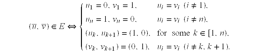
Diagrams of G2, G3 and G4 are shown in FIGS. 11,12 and 13, respectively. FIGS. 11A, 12A, and 13A illustrate wafer positioning within the cluster tool, where an empty circle represents an empty chamber and a circle containing a dot represents a chamber containing a wafer. Let f(n)=ΣCl(C), where the sum is over all cycles in Gn(V,E)and l(C)denotes the length of a cycle C. Direct enumeration (by an algorithm to be discussed in detail below) gives f(2)=6, f(3)=24, f(4)=180, f(5)=29,112, and j(6)=1,025,039,736.
A schedule is then a finite string {overscore (x)} . . . {overscore (u)}{overscore (v)} . . . {overscore (x)} corresponding to a cycle in Gn(V,E) that starts and ends at {overscore (x)}. Hence, f(n) is the total number of schedules. If {overscore (v)} is the immediate successor of {overscore (u)} in the schedule, then {overscore (u)} and {overscore (v)} differ in at most two coordinates, and v must be chosen according to the above rules (s1,s2,s3). These rules give rise to the requirements for ({overscore (u)},{overscore (v)})∈E(Gn).
A digraph Gn(V,E) defined above has the property that the length of each cycle in it is a multiple of n+1 where n is the number of stages. To see this, assign to each vertex {overscore (u)} a corresponding weight w({overscore (u)})=Σkkuk. From the above description of Gn(V,E), if ({overscore (u)}u,{overscore (v)}) is any edge of Gn(V,E), then either
1) w({overscore (v)})−w({overscore (u)})=1, or
2) w({overscore (v)})−w({overscore (u)})=−n.
Suppose there is a cycle of length r. If this cycle contains k edges ({overscore (u)},{overscore (v)}) where (2) above holds, then (r−k)×1+(−n)×k=0, and hence r=k×(n+1).
Distribution of cycle lengths in Gn(V,E) is not known. For example, all cycles in G2(V,E) have length three, all cycles in G3(V,E) have length four, and in G4(V,E) there are 24 cycles of length five and six cycles of length ten. The estimate for the length of the longest cycle in Gn(V,E)is not known either. At present, even the estimates or bounds for f(n) seem to be out of reach.
2) Mixed Wafer Flow
Without loss of generality, in a mixed wafer example, it is assumed that an n-chamber mixed wafer flow is comprised of k successive stages (or families), F1, F2, . . . , Fk, where k≦n. If 1,2, . . . , n are positions in a binary n-tuple {overscore (x)} that correspond to chambers C1, C 2, . . . , Cn, respectively, then make positions 1,2, . . . , |F1| correspond to chambers in stage (family) 1, positions |F1|+1,|F1|+2, . . . , |F1|+|F2| correspond to chambers in stage (family) 2, and so on. If chamber Ci belongs to stage (family) Ft, then the position i in the associated binary n-tuple {overscore (x)} belongs to Ft and write i∈Ft (while, in fact, i is one of the |Ft| consecutive positions in {overscore (x)}).
In this mixed flow example, s={m1,m2,m3} and the successor occupancy vector {overscore (v)}=s({overscore (u)}) is chosen according to the following rules:
m1) If for some i∈F1 and {overscore (u)}[i]=0, then {overscore (v)}[i]=1. For all k≠i, {overscore (v)}[k]={overscore (u)}[k].
m2) If for some i∈Fk {overscore (u)}[i]=1, then {overscore (v)}[i]=0. For all j≠i, {overscore (v)}[j]={overscore (u)}[j].
m3) If for some i∈Ft and for some j∈Ft+1 {overscore (u)}[i]=1 and {overscore (u)}[j]=0, then {overscore (v)}[i]=0 and {overscore (v)}[j]=1. For all r∉{i,j}, {overscore (v)}[r]={overscore (u)}[r].
For example, if |F1|=2 and |F2|=1, then s[(001)]={(101), (000), (011)} and s[(100)]=s[(010)]={(110), (001)}, which is quite different than the case |Ft|=1 for t=1,2,3. The above rules {m1,m2,m3} correspond to a wafer being moved from load-lock into the stage (family) 1, from the last stage (family) Fk into the load-lock, and from the stage (family) Ft into the next stage (family) Ft+1, respectively. Clearly, if |Ft=1 for all t=1,2, . . . , k, then {m1,m2,m3}={s 1,s2,s3}.
For mixed wafer flows, the two smallest possible configurations (two chambers in the first stage-and one in the second stage and vice versa) have been examined. Their associated digraphs are shown in FIGS. 14 and 15 and FIGS. 14A and 15A illustrate wafer positions within the cluster tools. The set of all schedules can be divided into equivalence classes under a “cyclic shift” operation. A class is comprised of a schedule Q and all schedules derived from Q by applying the successor occupancy vector rules m1,m2 and m3 so that all letters are on the same simple cycle of the associated digraph. By inspection, from FIGS. 14 and 15, it can be seen that for the smallest 2-stage mixed wafer flow schedules are either of length three or six.
As already mentioned, once the simple cycles are listed, the invention tests each cycle for throughput by using a throughput simulator. The cycle yielding maximum throughput is then deemed the optimum schedule. The importance of schedules found by the above method is that one cannot do better by scheduling wafers any other way. This conclusion can be formalized in the following statement:
The optimum schedule produced by evaluation of simple cycles is globally optimal, i.e., there is no cycle in the associated digraph G({0,1}n,E) yielding smaller throughput than the optimum simple cycle.
To prove the above statement, note that as wafers are being moved through the cluster tool, the digraph G({0,1}n,E), is being traversed (from a vertex {overscore (x)} to one of the vertices in s({overscore (x)}) to one of the vertices in s({overscore (y)}), where {overscore (y)}∈s({overscore (x)}), and so on). Hence, given a sufficient number of wafers, there will be a vertex in G({0,1}n,E) which is visited twice. (This is because the number of vertices in G({0,1}n,E) is 2n, where n is the number of chambers.) Any such cycle is a union of simple cycles and thus its corresponding throughput is the sum of throughputs of the simple cycles. It then follows from the fact that the sum of any M non-negative numbers (throughputs) is larger than M times the smallest number (throughput).
As discussed above, the problem of finding an optimum schedule calls for finding all simple cycles in G({0,1}n,E) whose vertices are occupancy-vectors from {0,1}n and whose edges are defined by either {s1,s2,s3} or by {m1,m2,m3} rules. That is, for any pair of vertices {overscore (x)},{overscore (y)}∈{0,1}n there is an edge from {overscore (x)} to {overscore (y)} if and only if {overscore (y)}∈s({overscore (x)}). The schedules then correspond to simple cycles in G({0,1}n,E).
The number of cycles in a digraph can be exponential in the number of vertices. For example, it is known that the complete digraph of n vertices and (n−1) edges contains 
cycles of length i for a total of 
cycles.
Another example of a digraph with exponential number of simple cycles is given in FIG. 16. In this case, however, the number of edges is substantially smaller than in case of a complete digraph. Thus, one can hardly expect an algorithm to be polynomial in the size of the input (here, the input has size 2n where n is the number of stages). However, algorithms can be produced that generate the cycles in time O((|V|+|E|)(c+1)), where c is the number of cycles in the digraph. Such an algorithm would be very good, since the time taken just to print the cycles must be L·c, where L is the average cycle length, which is upper bounded by number of vertices, i.e., L=O(|V|). These cycles can be enumerated in several ways as discussed below.
a) Recursive Enumeration
In order to ensure that each generated cycle is new, vertices are assumed to be represented as integers from 1 to |V|=2”, and each cycle is assumed to be rooted at the cycle's smallest vertex. FIG. 17 depicts a flow diagram of a recursive enumeration process 1700. The process begins at step 102 and proceeds to step 1704. At step 1704, a search begins at vertex s by building a directed path (s,v1,v2. . . , vk) at step 1706, such that vi>s for 1≦i≦k. A cycle is identified (and stored) only when the next vertex vk+1=s is identified. After generating the cycle (s,v1,v2, . . . ,vk,s), the next edge extending from vk is explored at step 1708. If all edges going out of vk have been explored, the process 1700 proceeds through query 1710 to the previous vertex vk−1 at step 1716 and attempts to list cycles from that vertex and so on. This process is continued through step 1710 until the process 1700 backs up past the starting vertex s; all cycles containing vertex s have then been generated. The process is repeated for every vertex s=1,2, . . . , |V| (i.e., until query 1712 is affirmatively answered). The process stops at step 1714.
To prevent traversing cycles that originate at a vertex vi during the search for cycles rooted at s, the process 1700 must exclude all vertices on the current path (except s) as extensions of that path. A vertex v will be marked as unavailable by setting avail(v) to false as soon as v is appended to the current path. The vertex v will remain unavailable at least until the process 1700 has backed up past v to the previous vertex on the current path. If the current path up to vertex v did not lead to a cycle rooted at s, v will remain unavailable for awhile even after the process backs up past it. This prevents searching for cycles in parts of the digraph on which such searches have been previously unsuccessful.
As the search progresses, the vertices on the current path are stored in a stack called path: a vertex v is added to the top of the stack before the search continues (by a recursive call) and is removed from the top of the stack in backing up (on return from the recursive call). The vertex is marked unavailable as the vertex is put on the stack and, if the vertex leads to a cycle rooted at s, made available again after the vertex is removed from the stack. If the process did not lead to a cycle rooted at s, then the cycle remains temporarily unavailable. A record is kept of the predecessors of all unavailable vertices that are not on the current path by maintaining sets B(w) for each w∈V:
B(w):={v∈V|(v,w) ∈ E and v is unavailable and not on the current path}
In other words, B(w)is the set of unavailable predecessors of w∈V. When the current path is (s,v1,v2, . . . , vk) and the next edge traversed is (vk,vk+1), there are three cases to consider:
1. If vk+1=s, a new cycle (s,v1,v2, . . . . . , vk,s) has been generated. The process outputs (e.g., print) the cycle and then set flag←true to indicate that a cycle (rooted at s) going through vk has been found.
2. If vk+1≠s and vk+1 is available, the process appends vk+1 to the current path by making a recursive call to the cycle generating procedure.
3. If vk+1 is unavailable, then the process ignores the cycle and looks for another edge starting at vk. If there are no unexplored edges starting at vk, vk is deleted from the path and the process backs up to vk−1. In backing up to vk−1, the process makes vk available again if it led to a cycle (i.e., if flag is true). Otherwise, the cycle is left unavailable and the vertices w that are successors of vk have vk added to their set B(w).
b) Digraph Generation Based On A Depth-First Search
In the case of generating a digraph using a depth-first search, a back edge of a digraph generated in a depth-first search corresponds to a simple cycle. A forward edge may correspond to a “short-cut” of a cycle. A cross edge (in the same tree) may correspond to one or more other simple cycles.
For example, in {0,1}2={(00), (01), (10), (11)} and serial wafer flow, edges are specified by the successor relationship as
s[(00)]={(10)}
s[(01)]={(11), (00)}
s[(10)]={(00)}
s[(11)]={(0)}
Thus, the set E in G({0,1}2,E) has five edges, namely ((00), (10)), ((01), (11)), ((01), (00)), ((10), (01)) and ((11), (10)), as shown in FIG. 11. There are only two distinct simple cycles of length three in the associated digraph. Since each k-cycle corresponds to k schedules, a 2-chamber serial wafer flow has six schedules.
The adjacency matrix shown in FIG. 18 that is associated with the digraph of FIG. 11 is a 4 by 4 binary matrix D such that D(x,y)=1 if and only if y∈s(x). There is, of course, a one-to-one correspondence between these two objects, i.e., given the adjacency matrix D it is possible to recover digraph G({0,1}2,E) within the isomorphism.
The adjacency matrix D for a two chamber serial wafer flow is given below. Note that, for example, D((01), (11))=1 because vertix (state) (11) is in the set s(01).
| |
| 00 | 01 | 10 | 11 | ||
| 00 | 0 | 0 | 1 | 0 |
| 01 | 1 | 0 | 0 | 1 |
| 10 | 0 | 1 | 0 | 0 |
| 11 | 0 | 0 | 1 | 0 |
By using matrices Dk for k=2,3, . . . it is easy to recognize paths or cycles of length k. For example, from the matrix D3 below,
| |
| 00 | 01 | 10 | 11 | ||
| 00 | 1 | 0 | 0 | 1 |
| 01 | 0 | 2 | 0 | 0 |
| 10 | 0 | 0 | 2 | 0 |
| 11 | 1 | 0 | 0 | 1 |
it is easy to see that associated digraph has two cycles of length three (vertices) (01) and (10) below to both cycles while vertices (00) and (11) are on only one cycle). The real advantage of this association is for large digraphs which have many cycles.
Digraph Generation Using A Backtrack Search
To find all cycles in a given digraph, the invention may use a simple backtrack search. Let {overscore (u)}1 be the starting vertex of a cycle. By using the rules for adding a successor vertix of a process builds a path, say S={overscore (u)}1{overscore (u)}2 . . . {overscore (u)}k. There are two questions the process must answer every time it appends a new vertex {overscore (u)}k+1 to path S:
a) Is {overscore (u)}1{overscore (u)}2 . . . {overscore (u)}k{overscore (u)}k+1 a cycle;
b) If {overscore (u)}1{overscore (u)}2 . . . {overscore (u)}k{overscore (u)}k+1 is a cycle, are there other cycles which have not been recorded.
A string {overscore (u)}1{overscore (u)}2 . . . {overscore (u)}k{overscore (u)}k+1 is a cycle if it is built according to rules for successor occupancy-vector, all vertices {overscore (u)}1{overscore (u)}2 . . . {overscore (u)}k+1 are different, and the successor of {overscore (u)}k+1 is the starting vertex {overscore (u)}1. If {overscore (u)}1{overscore (u)}k+2 . . . {overscore (u)}k{overscore (u)}k+1 happens to be a simple-cycle, the process stores the cycle (or print it), removes the vertex {overscore (u)}k+1 from the cycle and looks at some other unused successor of {overscore (u)}k. If there is such a successor, say {overscore (z)}, the process checks if {overscore (u)}1{overscore (u)}2 . . . {overscore (u)}k{overscore (z)} a cycle. If {overscore (u)}1{overscore (u)}2 . . . {overscore (u)}k{overscore (z)} is not a cycle, the process appends an unused successor of {overscore (z)} and so on. If {overscore (u)}1{overscore (u)}2 . . . {overscore (u)}k{overscore (z)} is a cycle, the process removes {overscore (z)} and look for another unused successor of {overscore (u)}k. If there are no unused successors of {overscore (u)}k, the process returns (backtracks) and looks at unused successors of {overscore (u)}k−1 and so on until the process returns to the starting vertex {overscore (u)}1. FIG. 19 depicts a flow diagram of the backtrack process 1900. The process performs the following sequence of steps:
Clearly, the process 1900 must ensure that the process doesn't produce duplicate cycles in Step 1908 as well as that the process have produced all possible cycles. The former is performed in Step 19010 where the process appends only an unused successor of the last vertex to the path. The latter is ensured by the proper termination condition (i.e., the process is at {overscore (u)}1 and there are no unused successors of {overscore (u)}1). To find all schedules, the process needs to the backtrack search for each vertex from {0,1}n. If α({overscore (x)}) is the number of cycles that start with the vertex {overscore (x)}, the total number of cycles is Σ{overscore (x)}∈{0,1} n α({overscore (x)}).
When chamber cleaning process is taken into account in the schedule generation process, a chamber has three states: 0 (empty chamber), 1 (wafer in chamber), and C (chamber undergoing a cleaning process). Only an empty chamber can initiate a cleaning process. When a cleaning process is over, a chamber either remains empty or a wafer is put in. FIG. 20 depicts digraph G1({0,1,C},E) that takes account of cleaning processes. FIG. 20 also depicts the digraph's corresponding adjacency matrix and an illustrative wafer positioning.
Due to a chamber cleaning process, the number of states increases considerably and is given by 3n where n is the number of stages. This is illustrated in FIG. 21 depicting a digraph, an adjacency matrix and illustrative wafer positioning in a cluster tool for a 2-chamber serial wafer flow with chamber clean. In the associated 9-vertex digraph, there are now seven cycles of length two, 4 cycles of length three, two cycles of length five, three cycles of length six, one cycle of length seven and one of length eight.
When a chamber cleaning process happens frequently (e.g. clean after processing every wafer), one must deal with the extended 3n-node digraph that accounts for “chamber-clean” state. The procedure however remains the same as described above. The process is only longer because the number of simple-cycles is bigger. When a chamber clean is infrequent, one can ignore the cleaning process and use the schedule obtained for 2-state chamber occupancy modified for the chamber clean. That is, every time a chamber clean happens, the cycle starts from a new vertex and is optimum until the next clean happens.
The present invention rapidly computes all possible schedules for a given cluster tool configuration. The schedules are then executed by a throughput model to determine the optimal schedule. As such, the present invention facilitates automatic determination of an optimal schedule in a rapid and accurate manner that has heretofore been unavailable in the prior art.
Although various embodiments which incorporate the teachings of the present invention have been shown and described in detail herein, those skilled in the art can readily devise many of the varied embodiments that still incorporate these teachings.
Claims (22)
1. A method of producing schedules for processing a wafer in a multichamber semiconductor wafer processing tool comprising the steps of:
(a) providing a trace defining a series of chambers that are visited by a wafer as the wafer is processed by the tool;
(b) initializing a sequence generator with an initial digraph vertex defining an initial wafer positioning with the tool; and
(c) generating vectors that represent all valid wafer movements related to the initial digraph vertex that lead to valid successor vertices, where said vectors and vertices, taken together, form a digraph that represents at least one schedule for processing a wafer.
2. The method of claim 1 wherein combinations of vertices and vectors form cycles in the digraph, where each cycle represents a schedule.
3. The method of claim 1 further comprising the steps of:
(d) backtracking through a set of vertices and applying step (c) to a prior vertex to produce further successor vertices and vectors; and
(e) stopping said backtracking when all possible cycles are produced that represent all possible valid schedules.
4. The method of claim 3 further comprising the step of:
(f) identifying at least one schedule in all possible valid schedules that provides an optimal throughput for a given trace.
5. The method of claim 4 wherein said identifying step (f) further comprises the step of computing the throughput for each and every schedule of said all possible schedules and selecting an optimum schedule for the trace which produces the highest throughput.
6. The method of claim 3 wherein said backtracking step (d) further comprises the steps of:
(a′) initializing a vertex;
(b′) identifying an unused successor vertex;
(c′) appending the unused successor vertex to a path;
(d′) querying whether the last vertex is the same as a previous vertex in the path and, if not, repeat steps (b′), (c′), and (d′) until the last vertex of the path is the same as some previous vertex in the path;
(e′) storing the path as a cycle;
(f′) querying whether any other cycles remain and, if not, stopping; otherwise, proceeding to step (g′);
(g′) removing the last vertex of the cycle;
(h′) querying whether there is an unused successor vertex and, if there are no unused successor vertices, repeating steps (f′), (g′) and (h′) until there is an unused successor vertex;
(i′) appending the unused successor vertex to a new path, marking the successor vertex as used; and
(k′) returning to step (b′).
7. The method of claim 6 wherein successor vertices are defined by successor generation rules that are prescribed by wafer processing parameters.
8. The method of claim 6 wherein successor vertices are generated with regard to transport-robot positioning.
9. Apparatus for producing schedules for processing a wafer in a multichamber semiconductor wafer processing tool, having a trace defining a series of chambers that are visited by a wafer as the wafer is processed by the tool, said apparatus comprising:
a sequence generator, being initialized with an initial value of a vertex defining an initial wafer positioning within the tool, for generating values of said vertex that represent all valid successor wafer positions related to the initial vertex, where said vertices and vectors connecting the vertices, taken together, form at least one cycle that represents a schedule for processing a wafer.
10. The apparatus of claim 9 further comprising a throughput model, coupled to said sequence generator, for computing a throughput value for each possible schedule in said all possible schedules.
11. The apparatus of claim 10 further comprising means for identifying at least one schedule that has the largest throughput value.
12. Apparatus for producing schedules for processing a wafer in a multichamber semiconductor wafer processing tool, having a trace defining a series of chambers that are visited by a wafer as the wafer is processed by the tool, said apparatus comprising:
(a) means for providing a trace defining a series of chambers that are visited by a wafer as the wafer is processed by the tool;
(b) means for initializing a sequence generator with an initial digraph vertex defining an initial wafer positioning with the tool; and
(c) means for generating vectors that represent all valid wafer movements related to the initial digraph vertex that lead to valid successor vertices, where said vectors and vertices, taken together, form a cycle that represents at least one schedule for processing a wafer.
13. The apparatus of claim 12 wherein combinations of vertices and vectors form cycles in the digraph, where each cycle represents a schedule.
14. The apparatus of claim 12 further comprising:
(d) means for backtracking through a set of vertices and applying said means for generating vectors to a prior vertex to produce further successor vertices and vectors; and
(e) means for stopping said backtracking when all possible cycles are produced that represent all possible valid schedules.
15. A computer readable memory containing software that, when executed by a processor, causes a sequence generator to perform a method of producing schedules for processing a wafer in a multichamber semiconductor wafer processing tool comprising the steps of:
(a) providing a trace defining a series of chambers that are visited by a wafer as the wafer is processed by the tool;
(b) initializing a sequence generator with an initial digraph vertex defining an initial wafer positioning with the tool; and
(c) generating vectors that represent all valid wafer movements related to the initial digraph vertex that lead to valid successor vertices, where said vectors and vertices, taken together, form a digraph that represents at least one schedule for processing a wafer.
16. The method of claim 15 wherein combinations of vertices and vectors form cycles in the digraph, where each cycle represents a schedule.
17. The method of claim 15 further comprising the steps of:
(d) backtracking through a set of vertices and applying step (c) to a prior vertex to produce further successor vertices and vectors; and
(e) stopping said backtracking when all possible cycles are produced that represent all possible valid schedules.
18. The method of claim 17 further comprising the step of:
(f) identifying at least one schedule in all possible valid schedules that provides an optimal throughput for a given trace.
19. The method of claim 18 wherein said identifying step (f) further comprises the step of computing the throughput for each and every schedule of said all possible schedules and selecting an optimum schedule for the trace which produces the highest throughput.
20. The method of claim 17 wherein said backtracking step (d) further comprises the steps of:
(a′) initializing a vertex;
(b′) identifying an unused successor vertex;
(c′) appending the unused successor vertex to a path;
(d′) querying whether the last vertex is the same as a previous vertex in the path and, if not, repeat steps (b′), (c′), and (d′) until the last vertex of the path is the same as some previous vertex in the path;
(e′) storing the path as a cycle;
(f′) querying whether any other cycles remain and, if not, stopping; otherwise, proceeding to step (g′);
(g′) removing the last vertex of the cycle;
(h′) querying whether there is an unused successor vertex and, if there are no unused successor vertices, repeating steps (f′), (g′) and (h′) until there is an unused successor vertex;
(i′) appending the unused successor vertex to a new path, marking the successor vertex as used; and
(j′) returning to step (b′).
21. The method of claim 20 wherein successor vertices are defined by successor generation rules that are implied by a wafer processing sequence.
22. The method of claim 20 wherein successor vertices are generated with regard to transport-robot positioning.
Priority Applications (3)
| Application Number | Priority Date | Filing Date | Title |
|---|---|---|---|
| US09/771,254 US6725114B1 (en) | 1997-06-09 | 2001-01-26 | Method and apparatus for automatically generating schedules for wafer processing within a multichamber semiconductor wafer processing tool |
| PCT/US2002/002378 WO2002059704A2 (en) | 2001-01-26 | 2002-01-28 | Method and apparatus for automatically generating schedules for wafer processing within a multichamber semiconductor wafer processing tool |
| TW091101415A TW526530B (en) | 2001-01-26 | 2002-01-28 | Method and apparatus for automatically generating schedules for wafer processing within a multichamber semiconductor wafer processing tool |
Applications Claiming Priority (2)
| Application Number | Priority Date | Filing Date | Title |
|---|---|---|---|
| US08/871,746 US6201999B1 (en) | 1997-06-09 | 1997-06-09 | Method and apparatus for automatically generating schedules for wafer processing within a multichamber semiconductor wafer processing tool |
| US09/771,254 US6725114B1 (en) | 1997-06-09 | 2001-01-26 | Method and apparatus for automatically generating schedules for wafer processing within a multichamber semiconductor wafer processing tool |
Related Parent Applications (1)
| Application Number | Title | Priority Date | Filing Date |
|---|---|---|---|
| US08/871,746 Continuation-In-Part US6201999B1 (en) | 1997-06-09 | 1997-06-09 | Method and apparatus for automatically generating schedules for wafer processing within a multichamber semiconductor wafer processing tool |
Publications (1)
| Publication Number | Publication Date |
|---|---|
| US6725114B1 true US6725114B1 (en) | 2004-04-20 |
Family
ID=25358037
Family Applications (3)
| Application Number | Title | Priority Date | Filing Date |
|---|---|---|---|
| US08/871,746 Expired - Fee Related US6201999B1 (en) | 1997-06-09 | 1997-06-09 | Method and apparatus for automatically generating schedules for wafer processing within a multichamber semiconductor wafer processing tool |
| US09/771,254 Expired - Fee Related US6725114B1 (en) | 1997-06-09 | 2001-01-26 | Method and apparatus for automatically generating schedules for wafer processing within a multichamber semiconductor wafer processing tool |
| US09/804,808 Expired - Fee Related US6496746B2 (en) | 1997-06-09 | 2001-03-13 | Method and apparatus for automatically generating schedules for wafer processing within a multichamber semiconductor wafer processing tool |
Family Applications Before (1)
| Application Number | Title | Priority Date | Filing Date |
|---|---|---|---|
| US08/871,746 Expired - Fee Related US6201999B1 (en) | 1997-06-09 | 1997-06-09 | Method and apparatus for automatically generating schedules for wafer processing within a multichamber semiconductor wafer processing tool |
Family Applications After (1)
| Application Number | Title | Priority Date | Filing Date |
|---|---|---|---|
| US09/804,808 Expired - Fee Related US6496746B2 (en) | 1997-06-09 | 2001-03-13 | Method and apparatus for automatically generating schedules for wafer processing within a multichamber semiconductor wafer processing tool |
Country Status (6)
| Country | Link |
|---|---|
| US (3) | US6201999B1 (en) |
| EP (1) | EP1021821A1 (en) |
| JP (1) | JP2002511193A (en) |
| KR (1) | KR20010013606A (en) |
| TW (1) | TW449793B (en) |
| WO (1) | WO1998057358A1 (en) |
Cited By (13)
| Publication number | Priority date | Publication date | Assignee | Title |
|---|---|---|---|---|
| US20030171972A1 (en) * | 2002-01-28 | 2003-09-11 | James Heskin | Scheduling system and method |
| US20060137609A1 (en) * | 2004-09-13 | 2006-06-29 | Puchacz Jerzy P | Multi-single wafer processing apparatus |
| US20070004052A1 (en) * | 2003-05-08 | 2007-01-04 | Tokyo Electron Limited | Processing schedule creaitng method, coating and developing apparatus, pattern forming apparatus and processing system |
| US20080260500A1 (en) * | 2007-02-27 | 2008-10-23 | Meulen Peter Van Der | Batch substrate handling |
| US20090138114A1 (en) * | 2005-05-11 | 2009-05-28 | Richard Gerard Burda | Method of release and product flow management for a manufacturing facility |
| US20090240366A1 (en) * | 2008-03-08 | 2009-09-24 | Tokyo Electron Limited | Method and system for detection of tool performance degradation and mismatch |
| US20100138026A1 (en) * | 2008-03-08 | 2010-06-03 | Tokyo Electron Limited | Method and apparatus for self-learning and self-improving a semiconductor manufacturing tool |
| US20100168892A1 (en) * | 2008-12-31 | 2010-07-01 | Kilian Schmidt | Method and system for synchronizing chamber down times by controlling transport sequencing in a process tool |
| US20110144792A1 (en) * | 2009-12-14 | 2011-06-16 | Teruo Nakata | Semiconductor processing system and program |
| US20140060735A1 (en) * | 2012-08-31 | 2014-03-06 | Samsung Display Co., Ltd. | Substrate processing apparatus |
| US9275335B2 (en) | 2008-03-08 | 2016-03-01 | Tokyo Electron Limited | Autonomous biologically based learning tool |
| US10043693B1 (en) | 2017-06-06 | 2018-08-07 | Applied Materials, Inc. | Method and apparatus for handling substrates in a processing system having a buffer chamber |
| US10073444B2 (en) * | 2015-09-20 | 2018-09-11 | Macau University Of Science And Technology | Petri net-based optimal one-wafer cyclic scheduling of treelike hybrid multi-cluster tools |
Families Citing this family (437)
| Publication number | Priority date | Publication date | Assignee | Title |
|---|---|---|---|---|
| US6201999B1 (en) * | 1997-06-09 | 2001-03-13 | Applied Materials, Inc. | Method and apparatus for automatically generating schedules for wafer processing within a multichamber semiconductor wafer processing tool |
| US6865437B1 (en) * | 1998-12-31 | 2005-03-08 | Asml Holdings N.V. | Robot pre-positioning in a wafer processing system |
| US6768930B2 (en) | 1998-12-31 | 2004-07-27 | Asml Holding N.V. | Method and apparatus for resolving conflicts in a substrate processing system |
| US6678572B1 (en) * | 1998-12-31 | 2004-01-13 | Asml Holdings, N.V. | Recipe cascading in a wafer processing system |
| US6418356B1 (en) | 1998-12-31 | 2002-07-09 | Silicon Valley Group, Inc. | Method and apparatus for resolving conflicts in a substrate processing system |
| US6556949B1 (en) | 1999-05-18 | 2003-04-29 | Applied Materials, Inc. | Semiconductor processing techniques |
| US6456894B1 (en) * | 1999-06-01 | 2002-09-24 | Applied Materials, Inc. | Semiconductor processing techniques |
| US6408220B1 (en) | 1999-06-01 | 2002-06-18 | Applied Materials, Inc. | Semiconductor processing techniques |
| AU5636600A (en) * | 1999-06-23 | 2001-01-09 | Silicon Valley Group, Inc. | Robot pre-positioning in a wafer processing system |
| US6889110B1 (en) | 1999-10-01 | 2005-05-03 | Novellus Systems, Inc. | Operational lists for simultaneous wafer scheduling and system event scheduling |
| JP2001159910A (en) * | 1999-12-03 | 2001-06-12 | Mitsubishi Electric Corp | System and method for selecting process device |
| WO2001054187A1 (en) * | 2000-01-17 | 2001-07-26 | Ebara Corporation | Wafer transfer control apparatus and method for transferring wafer |
| US6405144B1 (en) * | 2000-01-18 | 2002-06-11 | Advanced Micro Devices, Inc. | Method and apparatus for programmed latency for improving wafer-to-wafer uniformity |
| US6519498B1 (en) * | 2000-03-10 | 2003-02-11 | Applied Materials, Inc. | Method and apparatus for managing scheduling in a multiple cluster tool |
| DE10112681B4 (en) | 2000-03-31 | 2004-02-12 | International Business Machines Corp. | Computer system with methods for planning operations in a steel mill and program storage device for performing the method |
| US6952656B1 (en) | 2000-04-28 | 2005-10-04 | Applied Materials, Inc. | Wafer fabrication data acquisition and management systems |
| US6759255B2 (en) | 2000-05-10 | 2004-07-06 | Kla-Tencor Technologies Corp. | Method and system for detecting metal contamination on a semiconductor wafer |
| US7010788B1 (en) | 2000-05-19 | 2006-03-07 | Hewlett-Packard Development Company, L.P. | System for computing the optimal static schedule using the stored task execution costs with recent schedule execution costs |
| US6418350B1 (en) * | 2000-06-09 | 2002-07-09 | Brooks Automation Inc. | Periodic scheduler for dual-arm robots in cluster tools with process-module residency constraints |
| US6954716B2 (en) | 2000-07-07 | 2005-10-11 | Tokyo Electron Limited | Method of automatically resetting processing apparatus |
| EP1319244A1 (en) * | 2000-09-20 | 2003-06-18 | Kla-Tencor Inc. | Methods and systems for semiconductor fabrication processes |
| US6673637B2 (en) * | 2000-09-20 | 2004-01-06 | Kla-Tencor Technologies | Methods and systems for determining a presence of macro defects and overlay of a specimen |
| US6891627B1 (en) | 2000-09-20 | 2005-05-10 | Kla-Tencor Technologies Corp. | Methods and systems for determining a critical dimension and overlay of a specimen |
| US6812045B1 (en) | 2000-09-20 | 2004-11-02 | Kla-Tencor, Inc. | Methods and systems for determining a characteristic of a specimen prior to, during, or subsequent to ion implantation |
| US6694284B1 (en) | 2000-09-20 | 2004-02-17 | Kla-Tencor Technologies Corp. | Methods and systems for determining at least four properties of a specimen |
| US6782337B2 (en) * | 2000-09-20 | 2004-08-24 | Kla-Tencor Technologies Corp. | Methods and systems for determining a critical dimension an a presence of defects on a specimen |
| US6599368B1 (en) * | 2000-10-05 | 2003-07-29 | Applied Materials, Inc. | System architecture of semiconductor manufacturing equipment |
| US6560507B1 (en) | 2000-10-20 | 2003-05-06 | Novellus Systems Inc. | Module classification approach for moving semiconductor wafers in a wafer processing system |
| US20020142568A1 (en) * | 2001-03-27 | 2002-10-03 | Taiwan Semiconductor Manufacturing Co., Ltd., | Method and system for efficiently scheduling multi-chamber fabrication tool capacity |
| US7539630B2 (en) * | 2001-12-27 | 2009-05-26 | Jda Software Group | System, method, and computer program for replenishment by manufacture with attribute based planning |
| JP2003203963A (en) * | 2002-01-08 | 2003-07-18 | Tokyo Electron Ltd | Transport mechanism, processing system and transport method |
| US7236847B2 (en) * | 2002-01-16 | 2007-06-26 | Kla-Tencor Technologies Corp. | Systems and methods for closed loop defect reduction |
| US6701205B2 (en) | 2002-03-06 | 2004-03-02 | Massachusetts Institute Of Technology | System integration based on time-dependent periodic complexity |
| US6642151B2 (en) | 2002-03-06 | 2003-11-04 | Applied Materials, Inc | Techniques for plasma etching silicon-germanium |
| AU2003228859A1 (en) * | 2002-05-03 | 2003-11-17 | Manugistics, Inc. | Scheduling and sequencing supply chain resources |
| EP1523761A1 (en) * | 2002-06-21 | 2005-04-20 | Applied Materials, Inc. | Transfer chamber for vacuum processing system |
| US7012438B1 (en) | 2002-07-10 | 2006-03-14 | Kla-Tencor Technologies Corp. | Methods and systems for determining a property of an insulating film |
| US7064565B1 (en) | 2002-10-31 | 2006-06-20 | Kla-Tencor Technologies Corp. | Methods and systems for determining an electrical property of an insulating film |
| US7248062B1 (en) | 2002-11-04 | 2007-07-24 | Kla-Tencor Technologies Corp. | Contactless charge measurement of product wafers and control of corona generation and deposition |
| US20050221603A1 (en) * | 2003-06-23 | 2005-10-06 | Applied Materials, Inc. | System architecture of semiconductor manufacturing equipment |
| JP4209373B2 (en) * | 2003-10-13 | 2009-01-14 | エーエスエムエル ネザーランズ ビー.ブイ. | Lithographic apparatus or method of operating a lithographic processing cell, lithographic apparatus and lithographic processing cell |
| US7103484B1 (en) | 2003-10-31 | 2006-09-05 | Kla-Tencor Technologies Corp. | Non-contact methods for measuring electrical thickness and determining nitrogen content of insulating films |
| US6876894B1 (en) * | 2003-11-05 | 2005-04-05 | Taiwan Semiconductor Maufacturing Company, Ltd. | Forecast test-out of probed fabrication by using dispatching simulation method |
| US7646906B2 (en) * | 2004-01-29 | 2010-01-12 | Kla-Tencor Technologies Corp. | Computer-implemented methods for detecting defects in reticle design data |
| US7784164B2 (en) * | 2004-06-02 | 2010-08-31 | Applied Materials, Inc. | Electronic device manufacturing chamber method |
| TWI298895B (en) * | 2004-06-02 | 2008-07-11 | Applied Materials Inc | Electronic device manufacturing chamber and methods of forming the same |
| TWI231526B (en) * | 2004-06-23 | 2005-04-21 | Powerchip Semiconductor Corp | Chamber based dispatch method |
| US7477956B2 (en) * | 2004-07-12 | 2009-01-13 | Applied Materials, Inc. | Methods and apparatus for enhancing electronic device manufacturing throughput |
| US7266417B2 (en) * | 2004-09-03 | 2007-09-04 | Taiwan Semiconductor Manufacturing Company, Ltd. | System and method for semiconductor manufacturing automation |
| JP4904034B2 (en) * | 2004-09-14 | 2012-03-28 | ケーエルエー−テンカー コーポレイション | Method, system and carrier medium for evaluating reticle layout data |
| DE102005032601A1 (en) * | 2005-01-07 | 2006-07-20 | Heidelberger Druckmaschinen Ag | press |
| US20060167583A1 (en) * | 2005-01-22 | 2006-07-27 | Applied Materials, Inc. | Method and apparatus for on the fly positioning and continuous monitoring of a substrate in a chamber |
| US7769225B2 (en) | 2005-08-02 | 2010-08-03 | Kla-Tencor Technologies Corp. | Methods and systems for detecting defects in a reticle design pattern |
| WO2007022538A2 (en) * | 2005-08-19 | 2007-02-22 | Kla-Tencor Technologies Corporation | Test pads for measuring properties of a wafer |
| JP4884801B2 (en) * | 2005-10-06 | 2012-02-29 | 東京エレクトロン株式会社 | Processing system |
| US7570796B2 (en) * | 2005-11-18 | 2009-08-04 | Kla-Tencor Technologies Corp. | Methods and systems for utilizing design data in combination with inspection data |
| US7676077B2 (en) | 2005-11-18 | 2010-03-09 | Kla-Tencor Technologies Corp. | Methods and systems for utilizing design data in combination with inspection data |
| US8041103B2 (en) * | 2005-11-18 | 2011-10-18 | Kla-Tencor Technologies Corp. | Methods and systems for determining a position of inspection data in design data space |
| US7289860B1 (en) * | 2006-01-25 | 2007-10-30 | Advanced Micro Devices, Inc. | Method and apparatus for reserving a processing tool in a semiconductor fabrication facility |
| US20080025821A1 (en) * | 2006-07-25 | 2008-01-31 | Applied Materials, Inc. | Octagon transfer chamber |
| US7715936B2 (en) * | 2006-08-25 | 2010-05-11 | I-Factory Inc. | System and method for the production of goods or products |
| WO2008077100A2 (en) | 2006-12-19 | 2008-06-26 | Kla-Tencor Corporation | Systems and methods for creating inspection recipes |
| WO2008086282A2 (en) * | 2007-01-05 | 2008-07-17 | Kla-Tencor Corporation | Methods and systems for using electrical information for a device being fabricated on a wafer to perform one or more defect-related functions |
| JP5023146B2 (en) | 2007-04-20 | 2012-09-12 | 株式会社荏原製作所 | Polishing apparatus and program thereof |
| US7962863B2 (en) * | 2007-05-07 | 2011-06-14 | Kla-Tencor Corp. | Computer-implemented methods, systems, and computer-readable media for determining a model for predicting printability of reticle features on a wafer |
| US7738093B2 (en) | 2007-05-07 | 2010-06-15 | Kla-Tencor Corp. | Methods for detecting and classifying defects on a reticle |
| US8213704B2 (en) * | 2007-05-09 | 2012-07-03 | Kla-Tencor Corp. | Methods and systems for detecting defects in a reticle design pattern |
| US7796804B2 (en) * | 2007-07-20 | 2010-09-14 | Kla-Tencor Corp. | Methods for generating a standard reference die for use in a die to standard reference die inspection and methods for inspecting a wafer |
| US7711514B2 (en) * | 2007-08-10 | 2010-05-04 | Kla-Tencor Technologies Corp. | Computer-implemented methods, carrier media, and systems for generating a metrology sampling plan |
| JP5425779B2 (en) * | 2007-08-20 | 2014-02-26 | ケーエルエー−テンカー・コーポレーション | A computer-implemented method for determining whether an actual defect is a potential systematic defect or a potentially random defect |
| US8139844B2 (en) * | 2008-04-14 | 2012-03-20 | Kla-Tencor Corp. | Methods and systems for determining a defect criticality index for defects on wafers |
| US9659670B2 (en) | 2008-07-28 | 2017-05-23 | Kla-Tencor Corp. | Computer-implemented methods, computer-readable media, and systems for classifying defects detected in a memory device area on a wafer |
| JP5261085B2 (en) * | 2008-09-05 | 2013-08-14 | 東京エレクトロン株式会社 | Substrate placing mechanism, substrate processing apparatus, substrate placing mechanism control method, and storage medium |
| US10378106B2 (en) | 2008-11-14 | 2019-08-13 | Asm Ip Holding B.V. | Method of forming insulation film by modified PEALD |
| US8775101B2 (en) | 2009-02-13 | 2014-07-08 | Kla-Tencor Corp. | Detecting defects on a wafer |
| US8204297B1 (en) | 2009-02-27 | 2012-06-19 | Kla-Tencor Corp. | Methods and systems for classifying defects detected on a reticle |
| US8112241B2 (en) * | 2009-03-13 | 2012-02-07 | Kla-Tencor Corp. | Methods and systems for generating an inspection process for a wafer |
| US9394608B2 (en) | 2009-04-06 | 2016-07-19 | Asm America, Inc. | Semiconductor processing reactor and components thereof |
| US8802201B2 (en) | 2009-08-14 | 2014-08-12 | Asm America, Inc. | Systems and methods for thin-film deposition of metal oxides using excited nitrogen-oxygen species |
| US8483861B2 (en) * | 2009-08-31 | 2013-07-09 | Applied Materials, Inc. | Scheduling modeling system for adaptive, automated data collection and performance analysis of manufacturing system for optimal scheduling |
| US8655472B2 (en) | 2010-01-12 | 2014-02-18 | Ebara Corporation | Scheduler, substrate processing apparatus, and method of transferring substrates in substrate processing apparatus |
| JP5586271B2 (en) * | 2010-03-02 | 2014-09-10 | 株式会社日立ハイテクノロジーズ | Vacuum processing apparatus and program |
| JP5392190B2 (en) * | 2010-06-01 | 2014-01-22 | 東京エレクトロン株式会社 | Substrate processing system and substrate processing method |
| JP2012028659A (en) * | 2010-07-27 | 2012-02-09 | Hitachi High-Technologies Corp | Vacuum processing apparatus |
| US8781781B2 (en) | 2010-07-30 | 2014-07-15 | Kla-Tencor Corp. | Dynamic care areas |
| US9170211B2 (en) | 2011-03-25 | 2015-10-27 | Kla-Tencor Corp. | Design-based inspection using repeating structures |
| US9312155B2 (en) | 2011-06-06 | 2016-04-12 | Asm Japan K.K. | High-throughput semiconductor-processing apparatus equipped with multiple dual-chamber modules |
| US9793148B2 (en) | 2011-06-22 | 2017-10-17 | Asm Japan K.K. | Method for positioning wafers in multiple wafer transport |
| US10364496B2 (en) | 2011-06-27 | 2019-07-30 | Asm Ip Holding B.V. | Dual section module having shared and unshared mass flow controllers |
| US10854498B2 (en) | 2011-07-15 | 2020-12-01 | Asm Ip Holding B.V. | Wafer-supporting device and method for producing same |
| US20130023129A1 (en) | 2011-07-20 | 2013-01-24 | Asm America, Inc. | Pressure transmitter for a semiconductor processing environment |
| US9087367B2 (en) | 2011-09-13 | 2015-07-21 | Kla-Tencor Corp. | Determining design coordinates for wafer defects |
| US9096931B2 (en) | 2011-10-27 | 2015-08-04 | Asm America, Inc | Deposition valve assembly and method of heating the same |
| US9341296B2 (en) | 2011-10-27 | 2016-05-17 | Asm America, Inc. | Heater jacket for a fluid line |
| US9017481B1 (en) | 2011-10-28 | 2015-04-28 | Asm America, Inc. | Process feed management for semiconductor substrate processing |
| US9005539B2 (en) | 2011-11-23 | 2015-04-14 | Asm Ip Holding B.V. | Chamber sealing member |
| US9167625B2 (en) | 2011-11-23 | 2015-10-20 | Asm Ip Holding B.V. | Radiation shielding for a substrate holder |
| US9997384B2 (en) * | 2011-12-01 | 2018-06-12 | Taiwan Semiconductor Manufacturing Company, Ltd. | Methods for transporting wafers between wafer holders and chambers |
| US8831334B2 (en) | 2012-01-20 | 2014-09-09 | Kla-Tencor Corp. | Segmentation for wafer inspection |
| US9202727B2 (en) | 2012-03-02 | 2015-12-01 | ASM IP Holding | Susceptor heater shim |
| US8946830B2 (en) | 2012-04-04 | 2015-02-03 | Asm Ip Holdings B.V. | Metal oxide protective layer for a semiconductor device |
| JP5738796B2 (en) * | 2012-04-11 | 2015-06-24 | 株式会社日立ハイテクノロジーズ | Processing room assignment setting device and processing room assignment setting program |
| US9029253B2 (en) | 2012-05-02 | 2015-05-12 | Asm Ip Holding B.V. | Phase-stabilized thin films, structures and devices including the thin films, and methods of forming same |
| US8728832B2 (en) | 2012-05-07 | 2014-05-20 | Asm Ip Holdings B.V. | Semiconductor device dielectric interface layer |
| US8826200B2 (en) | 2012-05-25 | 2014-09-02 | Kla-Tencor Corp. | Alteration for wafer inspection |
| US8933375B2 (en) | 2012-06-27 | 2015-01-13 | Asm Ip Holding B.V. | Susceptor heater and method of heating a substrate |
| US9558931B2 (en) | 2012-07-27 | 2017-01-31 | Asm Ip Holding B.V. | System and method for gas-phase sulfur passivation of a semiconductor surface |
| US9117866B2 (en) | 2012-07-31 | 2015-08-25 | Asm Ip Holding B.V. | Apparatus and method for calculating a wafer position in a processing chamber under process conditions |
| US9659799B2 (en) | 2012-08-28 | 2017-05-23 | Asm Ip Holding B.V. | Systems and methods for dynamic semiconductor process scheduling |
| US9169975B2 (en) | 2012-08-28 | 2015-10-27 | Asm Ip Holding B.V. | Systems and methods for mass flow controller verification |
| US9021985B2 (en) | 2012-09-12 | 2015-05-05 | Asm Ip Holdings B.V. | Process gas management for an inductively-coupled plasma deposition reactor |
| US9324811B2 (en) | 2012-09-26 | 2016-04-26 | Asm Ip Holding B.V. | Structures and devices including a tensile-stressed silicon arsenic layer and methods of forming same |
| JP6002532B2 (en) * | 2012-10-10 | 2016-10-05 | 株式会社日立ハイテクノロジーズ | Vacuum processing apparatus and vacuum processing method |
| US10714315B2 (en) | 2012-10-12 | 2020-07-14 | Asm Ip Holdings B.V. | Semiconductor reaction chamber showerhead |
| US9189844B2 (en) | 2012-10-15 | 2015-11-17 | Kla-Tencor Corp. | Detecting defects on a wafer using defect-specific information |
| JP6094148B2 (en) * | 2012-10-29 | 2017-03-15 | 東京エレクトロン株式会社 | Substrate processing equipment |
| US9146551B2 (en) * | 2012-11-29 | 2015-09-29 | Asm Ip Holding B.V. | Scheduler for processing system |
| US9640416B2 (en) | 2012-12-26 | 2017-05-02 | Asm Ip Holding B.V. | Single-and dual-chamber module-attachable wafer-handling chamber |
| US9053527B2 (en) | 2013-01-02 | 2015-06-09 | Kla-Tencor Corp. | Detecting defects on a wafer |
| US9134254B2 (en) | 2013-01-07 | 2015-09-15 | Kla-Tencor Corp. | Determining a position of inspection system output in design data space |
| US9311698B2 (en) | 2013-01-09 | 2016-04-12 | Kla-Tencor Corp. | Detecting defects on a wafer using template image matching |
| US8894870B2 (en) | 2013-02-01 | 2014-11-25 | Asm Ip Holding B.V. | Multi-step method and apparatus for etching compounds containing a metal |
| WO2014149197A1 (en) | 2013-02-01 | 2014-09-25 | Kla-Tencor Corporation | Detecting defects on a wafer using defect-specific and multi-channel information |
| US9589770B2 (en) | 2013-03-08 | 2017-03-07 | Asm Ip Holding B.V. | Method and systems for in-situ formation of intermediate reactive species |
| US9484191B2 (en) | 2013-03-08 | 2016-11-01 | Asm Ip Holding B.V. | Pulsed remote plasma method and system |
| US9865512B2 (en) | 2013-04-08 | 2018-01-09 | Kla-Tencor Corp. | Dynamic design attributes for wafer inspection |
| US9310320B2 (en) | 2013-04-15 | 2016-04-12 | Kla-Tencor Corp. | Based sampling and binning for yield critical defects |
| US8993054B2 (en) | 2013-07-12 | 2015-03-31 | Asm Ip Holding B.V. | Method and system to reduce outgassing in a reaction chamber |
| US9018111B2 (en) | 2013-07-22 | 2015-04-28 | Asm Ip Holding B.V. | Semiconductor reaction chamber with plasma capabilities |
| US9793115B2 (en) | 2013-08-14 | 2017-10-17 | Asm Ip Holding B.V. | Structures and devices including germanium-tin films and methods of forming same |
| US9396934B2 (en) | 2013-08-14 | 2016-07-19 | Asm Ip Holding B.V. | Methods of forming films including germanium tin and structures and devices including the films |
| US9824318B1 (en) * | 2013-09-25 | 2017-11-21 | Amazon Technologies, Inc. | Generating labor requirements |
| US9240412B2 (en) | 2013-09-27 | 2016-01-19 | Asm Ip Holding B.V. | Semiconductor structure and device and methods of forming same using selective epitaxial process |
| US9556516B2 (en) | 2013-10-09 | 2017-01-31 | ASM IP Holding B.V | Method for forming Ti-containing film by PEALD using TDMAT or TDEAT |
| US9605343B2 (en) | 2013-11-13 | 2017-03-28 | Asm Ip Holding B.V. | Method for forming conformal carbon films, structures conformal carbon film, and system of forming same |
| US10179947B2 (en) | 2013-11-26 | 2019-01-15 | Asm Ip Holding B.V. | Method for forming conformal nitrided, oxidized, or carbonized dielectric film by atomic layer deposition |
| US10683571B2 (en) | 2014-02-25 | 2020-06-16 | Asm Ip Holding B.V. | Gas supply manifold and method of supplying gases to chamber using same |
| US9447498B2 (en) | 2014-03-18 | 2016-09-20 | Asm Ip Holding B.V. | Method for performing uniform processing in gas system-sharing multiple reaction chambers |
| US10167557B2 (en) | 2014-03-18 | 2019-01-01 | Asm Ip Holding B.V. | Gas distribution system, reactor including the system, and methods of using the same |
| US11015245B2 (en) | 2014-03-19 | 2021-05-25 | Asm Ip Holding B.V. | Gas-phase reactor and system having exhaust plenum and components thereof |
| JP2015211043A (en) * | 2014-04-23 | 2015-11-24 | 株式会社荏原製作所 | Substrate processing method |
| US9404587B2 (en) | 2014-04-24 | 2016-08-02 | ASM IP Holding B.V | Lockout tagout for semiconductor vacuum valve |
| US10858737B2 (en) | 2014-07-28 | 2020-12-08 | Asm Ip Holding B.V. | Showerhead assembly and components thereof |
| US9543180B2 (en) | 2014-08-01 | 2017-01-10 | Asm Ip Holding B.V. | Apparatus and method for transporting wafers between wafer carrier and process tool under vacuum |
| US9890456B2 (en) | 2014-08-21 | 2018-02-13 | Asm Ip Holding B.V. | Method and system for in situ formation of gas-phase compounds |
| US10941490B2 (en) | 2014-10-07 | 2021-03-09 | Asm Ip Holding B.V. | Multiple temperature range susceptor, assembly, reactor and system including the susceptor, and methods of using the same |
| US9657845B2 (en) | 2014-10-07 | 2017-05-23 | Asm Ip Holding B.V. | Variable conductance gas distribution apparatus and method |
| KR102300403B1 (en) | 2014-11-19 | 2021-09-09 | 에이에스엠 아이피 홀딩 비.브이. | Method of depositing thin film |
| KR102263121B1 (en) | 2014-12-22 | 2021-06-09 | 에이에스엠 아이피 홀딩 비.브이. | Semiconductor device and manufacuring method thereof |
| KR102296919B1 (en) * | 2015-01-16 | 2021-09-02 | 삼성디스플레이 주식회사 | Thin film encapsulation manufacturing device and manufacturing method of thin film encapsulation |
| US9478415B2 (en) | 2015-02-13 | 2016-10-25 | Asm Ip Holding B.V. | Method for forming film having low resistance and shallow junction depth |
| US10529542B2 (en) | 2015-03-11 | 2020-01-07 | Asm Ip Holdings B.V. | Cross-flow reactor and method |
| US10276355B2 (en) | 2015-03-12 | 2019-04-30 | Asm Ip Holding B.V. | Multi-zone reactor, system including the reactor, and method of using the same |
| US10458018B2 (en) | 2015-06-26 | 2019-10-29 | Asm Ip Holding B.V. | Structures including metal carbide material, devices including the structures, and methods of forming same |
| US10600673B2 (en) | 2015-07-07 | 2020-03-24 | Asm Ip Holding B.V. | Magnetic susceptor to baseplate seal |
| US10043661B2 (en) | 2015-07-13 | 2018-08-07 | Asm Ip Holding B.V. | Method for protecting layer by forming hydrocarbon-based extremely thin film |
| US9899291B2 (en) | 2015-07-13 | 2018-02-20 | Asm Ip Holding B.V. | Method for protecting layer by forming hydrocarbon-based extremely thin film |
| US10083836B2 (en) | 2015-07-24 | 2018-09-25 | Asm Ip Holding B.V. | Formation of boron-doped titanium metal films with high work function |
| US10087525B2 (en) | 2015-08-04 | 2018-10-02 | Asm Ip Holding B.V. | Variable gap hard stop design |
| US9647114B2 (en) | 2015-08-14 | 2017-05-09 | Asm Ip Holding B.V. | Methods of forming highly p-type doped germanium tin films and structures and devices including the films |
| US9711345B2 (en) | 2015-08-25 | 2017-07-18 | Asm Ip Holding B.V. | Method for forming aluminum nitride-based film by PEALD |
| US10295979B2 (en) * | 2015-09-15 | 2019-05-21 | Applied Materials, Inc. | Scheduling in manufacturing environments |
| US9960072B2 (en) | 2015-09-29 | 2018-05-01 | Asm Ip Holding B.V. | Variable adjustment for precise matching of multiple chamber cavity housings |
| US9909214B2 (en) | 2015-10-15 | 2018-03-06 | Asm Ip Holding B.V. | Method for depositing dielectric film in trenches by PEALD |
| US10211308B2 (en) | 2015-10-21 | 2019-02-19 | Asm Ip Holding B.V. | NbMC layers |
| US10322384B2 (en) | 2015-11-09 | 2019-06-18 | Asm Ip Holding B.V. | Counter flow mixer for process chamber |
| US9455138B1 (en) | 2015-11-10 | 2016-09-27 | Asm Ip Holding B.V. | Method for forming dielectric film in trenches by PEALD using H-containing gas |
| US9905420B2 (en) | 2015-12-01 | 2018-02-27 | Asm Ip Holding B.V. | Methods of forming silicon germanium tin films and structures and devices including the films |
| US9607837B1 (en) | 2015-12-21 | 2017-03-28 | Asm Ip Holding B.V. | Method for forming silicon oxide cap layer for solid state diffusion process |
| US9735024B2 (en) | 2015-12-28 | 2017-08-15 | Asm Ip Holding B.V. | Method of atomic layer etching using functional group-containing fluorocarbon |
| US9627221B1 (en) | 2015-12-28 | 2017-04-18 | Asm Ip Holding B.V. | Continuous process incorporating atomic layer etching |
| US11139308B2 (en) | 2015-12-29 | 2021-10-05 | Asm Ip Holding B.V. | Atomic layer deposition of III-V compounds to form V-NAND devices |
| US10468251B2 (en) | 2016-02-19 | 2019-11-05 | Asm Ip Holding B.V. | Method for forming spacers using silicon nitride film for spacer-defined multiple patterning |
| US10529554B2 (en) | 2016-02-19 | 2020-01-07 | Asm Ip Holding B.V. | Method for forming silicon nitride film selectively on sidewalls or flat surfaces of trenches |
| US9754779B1 (en) | 2016-02-19 | 2017-09-05 | Asm Ip Holding B.V. | Method for forming silicon nitride film selectively on sidewalls or flat surfaces of trenches |
| US10501866B2 (en) | 2016-03-09 | 2019-12-10 | Asm Ip Holding B.V. | Gas distribution apparatus for improved film uniformity in an epitaxial system |
| US10343920B2 (en) | 2016-03-18 | 2019-07-09 | Asm Ip Holding B.V. | Aligned carbon nanotubes |
| US9892913B2 (en) | 2016-03-24 | 2018-02-13 | Asm Ip Holding B.V. | Radial and thickness control via biased multi-port injection settings |
| US10087522B2 (en) | 2016-04-21 | 2018-10-02 | Asm Ip Holding B.V. | Deposition of metal borides |
| US10865475B2 (en) | 2016-04-21 | 2020-12-15 | Asm Ip Holding B.V. | Deposition of metal borides and silicides |
| US10190213B2 (en) | 2016-04-21 | 2019-01-29 | Asm Ip Holding B.V. | Deposition of metal borides |
| US10367080B2 (en) | 2016-05-02 | 2019-07-30 | Asm Ip Holding B.V. | Method of forming a germanium oxynitride film |
| US10032628B2 (en) | 2016-05-02 | 2018-07-24 | Asm Ip Holding B.V. | Source/drain performance through conformal solid state doping |
| KR102592471B1 (en) | 2016-05-17 | 2023-10-20 | 에이에스엠 아이피 홀딩 비.브이. | Method of forming metal interconnection and method of fabricating semiconductor device using the same |
| US11453943B2 (en) | 2016-05-25 | 2022-09-27 | Asm Ip Holding B.V. | Method for forming carbon-containing silicon/metal oxide or nitride film by ALD using silicon precursor and hydrocarbon precursor |
| US10388509B2 (en) | 2016-06-28 | 2019-08-20 | Asm Ip Holding B.V. | Formation of epitaxial layers via dislocation filtering |
| US9859151B1 (en) | 2016-07-08 | 2018-01-02 | Asm Ip Holding B.V. | Selective film deposition method to form air gaps |
| US10612137B2 (en) | 2016-07-08 | 2020-04-07 | Asm Ip Holdings B.V. | Organic reactants for atomic layer deposition |
| US9793135B1 (en) | 2016-07-14 | 2017-10-17 | ASM IP Holding B.V | Method of cyclic dry etching using etchant film |
| US10714385B2 (en) | 2016-07-19 | 2020-07-14 | Asm Ip Holding B.V. | Selective deposition of tungsten |
| US10381226B2 (en) | 2016-07-27 | 2019-08-13 | Asm Ip Holding B.V. | Method of processing substrate |
| US9812320B1 (en) | 2016-07-28 | 2017-11-07 | Asm Ip Holding B.V. | Method and apparatus for filling a gap |
| US9887082B1 (en) | 2016-07-28 | 2018-02-06 | Asm Ip Holding B.V. | Method and apparatus for filling a gap |
| KR102532607B1 (en) | 2016-07-28 | 2023-05-15 | 에이에스엠 아이피 홀딩 비.브이. | Substrate processing apparatus and method of operating the same |
| US10395919B2 (en) | 2016-07-28 | 2019-08-27 | Asm Ip Holding B.V. | Method and apparatus for filling a gap |
| US10177025B2 (en) | 2016-07-28 | 2019-01-08 | Asm Ip Holding B.V. | Method and apparatus for filling a gap |
| US10090316B2 (en) | 2016-09-01 | 2018-10-02 | Asm Ip Holding B.V. | 3D stacked multilayer semiconductor memory using doped select transistor channel |
| US10410943B2 (en) | 2016-10-13 | 2019-09-10 | Asm Ip Holding B.V. | Method for passivating a surface of a semiconductor and related systems |
| US10643826B2 (en) | 2016-10-26 | 2020-05-05 | Asm Ip Holdings B.V. | Methods for thermally calibrating reaction chambers |
| US11532757B2 (en) | 2016-10-27 | 2022-12-20 | Asm Ip Holding B.V. | Deposition of charge trapping layers |
| US10643904B2 (en) | 2016-11-01 | 2020-05-05 | Asm Ip Holdings B.V. | Methods for forming a semiconductor device and related semiconductor device structures |
| US10714350B2 (en) | 2016-11-01 | 2020-07-14 | ASM IP Holdings, B.V. | Methods for forming a transition metal niobium nitride film on a substrate by atomic layer deposition and related semiconductor device structures |
| US10229833B2 (en) | 2016-11-01 | 2019-03-12 | Asm Ip Holding B.V. | Methods for forming a transition metal nitride film on a substrate by atomic layer deposition and related semiconductor device structures |
| US10435790B2 (en) | 2016-11-01 | 2019-10-08 | Asm Ip Holding B.V. | Method of subatmospheric plasma-enhanced ALD using capacitively coupled electrodes with narrow gap |
| US10134757B2 (en) | 2016-11-07 | 2018-11-20 | Asm Ip Holding B.V. | Method of processing a substrate and a device manufactured by using the method |
| KR102546317B1 (en) | 2016-11-15 | 2023-06-21 | 에이에스엠 아이피 홀딩 비.브이. | Gas supply unit and substrate processing apparatus including the same |
| US10340135B2 (en) | 2016-11-28 | 2019-07-02 | Asm Ip Holding B.V. | Method of topologically restricted plasma-enhanced cyclic deposition of silicon or metal nitride |
| KR20180068582A (en) | 2016-12-14 | 2018-06-22 | 에이에스엠 아이피 홀딩 비.브이. | Substrate processing apparatus |
| US9916980B1 (en) | 2016-12-15 | 2018-03-13 | Asm Ip Holding B.V. | Method of forming a structure on a substrate |
| US11581186B2 (en) | 2016-12-15 | 2023-02-14 | Asm Ip Holding B.V. | Sequential infiltration synthesis apparatus |
| US11447861B2 (en) | 2016-12-15 | 2022-09-20 | Asm Ip Holding B.V. | Sequential infiltration synthesis apparatus and a method of forming a patterned structure |
| KR20180070971A (en) | 2016-12-19 | 2018-06-27 | 에이에스엠 아이피 홀딩 비.브이. | Substrate processing apparatus |
| US10269558B2 (en) | 2016-12-22 | 2019-04-23 | Asm Ip Holding B.V. | Method of forming a structure on a substrate |
| US10867788B2 (en) | 2016-12-28 | 2020-12-15 | Asm Ip Holding B.V. | Method of forming a structure on a substrate |
| US11390950B2 (en) | 2017-01-10 | 2022-07-19 | Asm Ip Holding B.V. | Reactor system and method to reduce residue buildup during a film deposition process |
| US10655221B2 (en) | 2017-02-09 | 2020-05-19 | Asm Ip Holding B.V. | Method for depositing oxide film by thermal ALD and PEALD |
| US10468261B2 (en) | 2017-02-15 | 2019-11-05 | Asm Ip Holding B.V. | Methods for forming a metallic film on a substrate by cyclical deposition and related semiconductor device structures |
| US10283353B2 (en) | 2017-03-29 | 2019-05-07 | Asm Ip Holding B.V. | Method of reforming insulating film deposited on substrate with recess pattern |
| US10529563B2 (en) | 2017-03-29 | 2020-01-07 | Asm Ip Holdings B.V. | Method for forming doped metal oxide films on a substrate by cyclical deposition and related semiconductor device structures |
| US10103040B1 (en) | 2017-03-31 | 2018-10-16 | Asm Ip Holding B.V. | Apparatus and method for manufacturing a semiconductor device |
| USD830981S1 (en) | 2017-04-07 | 2018-10-16 | Asm Ip Holding B.V. | Susceptor for semiconductor substrate processing apparatus |
| KR102457289B1 (en) | 2017-04-25 | 2022-10-21 | 에이에스엠 아이피 홀딩 비.브이. | Method for depositing a thin film and manufacturing a semiconductor device |
| US10770286B2 (en) | 2017-05-08 | 2020-09-08 | Asm Ip Holdings B.V. | Methods for selectively forming a silicon nitride film on a substrate and related semiconductor device structures |
| US10446393B2 (en) | 2017-05-08 | 2019-10-15 | Asm Ip Holding B.V. | Methods for forming silicon-containing epitaxial layers and related semiconductor device structures |
| US10892156B2 (en) | 2017-05-08 | 2021-01-12 | Asm Ip Holding B.V. | Methods for forming a silicon nitride film on a substrate and related semiconductor device structures |
| US10504742B2 (en) | 2017-05-31 | 2019-12-10 | Asm Ip Holding B.V. | Method of atomic layer etching using hydrogen plasma |
| US10886123B2 (en) | 2017-06-02 | 2021-01-05 | Asm Ip Holding B.V. | Methods for forming low temperature semiconductor layers and related semiconductor device structures |
| US11306395B2 (en) | 2017-06-28 | 2022-04-19 | Asm Ip Holding B.V. | Methods for depositing a transition metal nitride film on a substrate by atomic layer deposition and related deposition apparatus |
| US10685834B2 (en) | 2017-07-05 | 2020-06-16 | Asm Ip Holdings B.V. | Methods for forming a silicon germanium tin layer and related semiconductor device structures |
| KR20190009245A (en) | 2017-07-18 | 2019-01-28 | 에이에스엠 아이피 홀딩 비.브이. | Methods for forming a semiconductor device structure and related semiconductor device structures |
| US10541333B2 (en) | 2017-07-19 | 2020-01-21 | Asm Ip Holding B.V. | Method for depositing a group IV semiconductor and related semiconductor device structures |
| US11374112B2 (en) | 2017-07-19 | 2022-06-28 | Asm Ip Holding B.V. | Method for depositing a group IV semiconductor and related semiconductor device structures |
| US11018002B2 (en) | 2017-07-19 | 2021-05-25 | Asm Ip Holding B.V. | Method for selectively depositing a Group IV semiconductor and related semiconductor device structures |
| US10605530B2 (en) | 2017-07-26 | 2020-03-31 | Asm Ip Holding B.V. | Assembly of a liner and a flange for a vertical furnace as well as the liner and the vertical furnace |
| US10312055B2 (en) | 2017-07-26 | 2019-06-04 | Asm Ip Holding B.V. | Method of depositing film by PEALD using negative bias |
| US10590535B2 (en) | 2017-07-26 | 2020-03-17 | Asm Ip Holdings B.V. | Chemical treatment, deposition and/or infiltration apparatus and method for using the same |
| US10770336B2 (en) | 2017-08-08 | 2020-09-08 | Asm Ip Holding B.V. | Substrate lift mechanism and reactor including same |
| US10692741B2 (en) | 2017-08-08 | 2020-06-23 | Asm Ip Holdings B.V. | Radiation shield |
| US11769682B2 (en) | 2017-08-09 | 2023-09-26 | Asm Ip Holding B.V. | Storage apparatus for storing cassettes for substrates and processing apparatus equipped therewith |
| US11139191B2 (en) | 2017-08-09 | 2021-10-05 | Asm Ip Holding B.V. | Storage apparatus for storing cassettes for substrates and processing apparatus equipped therewith |
| US10249524B2 (en) | 2017-08-09 | 2019-04-02 | Asm Ip Holding B.V. | Cassette holder assembly for a substrate cassette and holding member for use in such assembly |
| US10236177B1 (en) | 2017-08-22 | 2019-03-19 | ASM IP Holding B.V.. | Methods for depositing a doped germanium tin semiconductor and related semiconductor device structures |
| USD900036S1 (en) | 2017-08-24 | 2020-10-27 | Asm Ip Holding B.V. | Heater electrical connector and adapter |
| US11830730B2 (en) | 2017-08-29 | 2023-11-28 | Asm Ip Holding B.V. | Layer forming method and apparatus |
| US11295980B2 (en) | 2017-08-30 | 2022-04-05 | Asm Ip Holding B.V. | Methods for depositing a molybdenum metal film over a dielectric surface of a substrate by a cyclical deposition process and related semiconductor device structures |
| US11056344B2 (en) | 2017-08-30 | 2021-07-06 | Asm Ip Holding B.V. | Layer forming method |
| KR102491945B1 (en) | 2017-08-30 | 2023-01-26 | 에이에스엠 아이피 홀딩 비.브이. | Substrate processing apparatus |
| US10359769B2 (en) | 2017-09-15 | 2019-07-23 | Applied Materials, Inc. | Substrate routing and throughput modeling |
| US10607895B2 (en) | 2017-09-18 | 2020-03-31 | Asm Ip Holdings B.V. | Method for forming a semiconductor device structure comprising a gate fill metal |
| KR102630301B1 (en) | 2017-09-21 | 2024-01-29 | 에이에스엠 아이피 홀딩 비.브이. | Method of sequential infiltration synthesis treatment of infiltrateable material and structures and devices formed using same |
| US10844484B2 (en) | 2017-09-22 | 2020-11-24 | Asm Ip Holding B.V. | Apparatus for dispensing a vapor phase reactant to a reaction chamber and related methods |
| US10658205B2 (en) | 2017-09-28 | 2020-05-19 | Asm Ip Holdings B.V. | Chemical dispensing apparatus and methods for dispensing a chemical to a reaction chamber |
| US10403504B2 (en) | 2017-10-05 | 2019-09-03 | Asm Ip Holding B.V. | Method for selectively depositing a metallic film on a substrate |
| US10319588B2 (en) | 2017-10-10 | 2019-06-11 | Asm Ip Holding B.V. | Method for depositing a metal chalcogenide on a substrate by cyclical deposition |
| US10923344B2 (en) | 2017-10-30 | 2021-02-16 | Asm Ip Holding B.V. | Methods for forming a semiconductor structure and related semiconductor structures |
| US10910262B2 (en) | 2017-11-16 | 2021-02-02 | Asm Ip Holding B.V. | Method of selectively depositing a capping layer structure on a semiconductor device structure |
| KR102443047B1 (en) | 2017-11-16 | 2022-09-14 | 에이에스엠 아이피 홀딩 비.브이. | Method of processing a substrate and a device manufactured by the same |
| US11022879B2 (en) | 2017-11-24 | 2021-06-01 | Asm Ip Holding B.V. | Method of forming an enhanced unexposed photoresist layer |
| JP7206265B2 (en) | 2017-11-27 | 2023-01-17 | エーエスエム アイピー ホールディング ビー.ブイ. | Equipment with a clean mini-environment |
| CN111316417B (en) | 2017-11-27 | 2023-12-22 | 阿斯莫Ip控股公司 | Storage device for storing wafer cassettes for use with batch ovens |
| US10290508B1 (en) | 2017-12-05 | 2019-05-14 | Asm Ip Holding B.V. | Method for forming vertical spacers for spacer-defined patterning |
| US10872771B2 (en) | 2018-01-16 | 2020-12-22 | Asm Ip Holding B. V. | Method for depositing a material film on a substrate within a reaction chamber by a cyclical deposition process and related device structures |
| CN111630203A (en) | 2018-01-19 | 2020-09-04 | Asm Ip私人控股有限公司 | Method for depositing gap filling layer by plasma auxiliary deposition |
| TW202325889A (en) | 2018-01-19 | 2023-07-01 | 荷蘭商Asm 智慧財產控股公司 | Deposition method |
| USD903477S1 (en) | 2018-01-24 | 2020-12-01 | Asm Ip Holdings B.V. | Metal clamp |
| US11018047B2 (en) | 2018-01-25 | 2021-05-25 | Asm Ip Holding B.V. | Hybrid lift pin |
| US10535516B2 (en) | 2018-02-01 | 2020-01-14 | Asm Ip Holdings B.V. | Method for depositing a semiconductor structure on a surface of a substrate and related semiconductor structures |
| USD880437S1 (en) | 2018-02-01 | 2020-04-07 | Asm Ip Holding B.V. | Gas supply plate for semiconductor manufacturing apparatus |
| US11081345B2 (en) | 2018-02-06 | 2021-08-03 | Asm Ip Holding B.V. | Method of post-deposition treatment for silicon oxide film |
| WO2019158960A1 (en) | 2018-02-14 | 2019-08-22 | Asm Ip Holding B.V. | A method for depositing a ruthenium-containing film on a substrate by a cyclical deposition process |
| US10896820B2 (en) | 2018-02-14 | 2021-01-19 | Asm Ip Holding B.V. | Method for depositing a ruthenium-containing film on a substrate by a cyclical deposition process |
| US10731249B2 (en) | 2018-02-15 | 2020-08-04 | Asm Ip Holding B.V. | Method of forming a transition metal containing film on a substrate by a cyclical deposition process, a method for supplying a transition metal halide compound to a reaction chamber, and related vapor deposition apparatus |
| KR102636427B1 (en) | 2018-02-20 | 2024-02-13 | 에이에스엠 아이피 홀딩 비.브이. | Substrate processing method and apparatus |
| US10658181B2 (en) | 2018-02-20 | 2020-05-19 | Asm Ip Holding B.V. | Method of spacer-defined direct patterning in semiconductor fabrication |
| US10975470B2 (en) | 2018-02-23 | 2021-04-13 | Asm Ip Holding B.V. | Apparatus for detecting or monitoring for a chemical precursor in a high temperature environment |
| US11473195B2 (en) | 2018-03-01 | 2022-10-18 | Asm Ip Holding B.V. | Semiconductor processing apparatus and a method for processing a substrate |
| US11629406B2 (en) | 2018-03-09 | 2023-04-18 | Asm Ip Holding B.V. | Semiconductor processing apparatus comprising one or more pyrometers for measuring a temperature of a substrate during transfer of the substrate |
| US11114283B2 (en) | 2018-03-16 | 2021-09-07 | Asm Ip Holding B.V. | Reactor, system including the reactor, and methods of manufacturing and using same |
| KR102646467B1 (en) | 2018-03-27 | 2024-03-11 | 에이에스엠 아이피 홀딩 비.브이. | Method of forming an electrode on a substrate and a semiconductor device structure including an electrode |
| US11230766B2 (en) | 2018-03-29 | 2022-01-25 | Asm Ip Holding B.V. | Substrate processing apparatus and method |
| US10510536B2 (en) | 2018-03-29 | 2019-12-17 | Asm Ip Holding B.V. | Method of depositing a co-doped polysilicon film on a surface of a substrate within a reaction chamber |
| US11088002B2 (en) | 2018-03-29 | 2021-08-10 | Asm Ip Holding B.V. | Substrate rack and a substrate processing system and method |
| KR102501472B1 (en) | 2018-03-30 | 2023-02-20 | 에이에스엠 아이피 홀딩 비.브이. | Substrate processing method |
| KR20190128558A (en) | 2018-05-08 | 2019-11-18 | 에이에스엠 아이피 홀딩 비.브이. | Methods for depositing an oxide film on a substrate by a cyclical deposition process and related device structures |
| TW202349473A (en) | 2018-05-11 | 2023-12-16 | 荷蘭商Asm Ip私人控股有限公司 | Methods for forming a doped metal carbide film on a substrate and related semiconductor device structures |
| KR102596988B1 (en) | 2018-05-28 | 2023-10-31 | 에이에스엠 아이피 홀딩 비.브이. | Method of processing a substrate and a device manufactured by the same |
| TW202013553A (en) | 2018-06-04 | 2020-04-01 | 荷蘭商Asm 智慧財產控股公司 | Wafer handling chamber with moisture reduction |
| US11718913B2 (en) | 2018-06-04 | 2023-08-08 | Asm Ip Holding B.V. | Gas distribution system and reactor system including same |
| US11286562B2 (en) | 2018-06-08 | 2022-03-29 | Asm Ip Holding B.V. | Gas-phase chemical reactor and method of using same |
| US10797133B2 (en) | 2018-06-21 | 2020-10-06 | Asm Ip Holding B.V. | Method for depositing a phosphorus doped silicon arsenide film and related semiconductor device structures |
| KR102568797B1 (en) | 2018-06-21 | 2023-08-21 | 에이에스엠 아이피 홀딩 비.브이. | Substrate processing system |
| US10698392B2 (en) * | 2018-06-22 | 2020-06-30 | Applied Materials, Inc. | Using graphics processing unit for substrate routing and throughput modeling |
| WO2020003000A1 (en) | 2018-06-27 | 2020-01-02 | Asm Ip Holding B.V. | Cyclic deposition methods for forming metal-containing material and films and structures including the metal-containing material |
| CN112292478A (en) | 2018-06-27 | 2021-01-29 | Asm Ip私人控股有限公司 | Cyclic deposition methods for forming metal-containing materials and films and structures containing metal-containing materials |
| US10612136B2 (en) | 2018-06-29 | 2020-04-07 | ASM IP Holding, B.V. | Temperature-controlled flange and reactor system including same |
| KR20200002519A (en) | 2018-06-29 | 2020-01-08 | 에이에스엠 아이피 홀딩 비.브이. | Method for depositing a thin film and manufacturing a semiconductor device |
| US10755922B2 (en) | 2018-07-03 | 2020-08-25 | Asm Ip Holding B.V. | Method for depositing silicon-free carbon-containing film as gap-fill layer by pulse plasma-assisted deposition |
| US10388513B1 (en) | 2018-07-03 | 2019-08-20 | Asm Ip Holding B.V. | Method for depositing silicon-free carbon-containing film as gap-fill layer by pulse plasma-assisted deposition |
| US10767789B2 (en) | 2018-07-16 | 2020-09-08 | Asm Ip Holding B.V. | Diaphragm valves, valve components, and methods for forming valve components |
| US10483099B1 (en) | 2018-07-26 | 2019-11-19 | Asm Ip Holding B.V. | Method for forming thermally stable organosilicon polymer film |
| US11053591B2 (en) | 2018-08-06 | 2021-07-06 | Asm Ip Holding B.V. | Multi-port gas injection system and reactor system including same |
| US10883175B2 (en) | 2018-08-09 | 2021-01-05 | Asm Ip Holding B.V. | Vertical furnace for processing substrates and a liner for use therein |
| US10829852B2 (en) | 2018-08-16 | 2020-11-10 | Asm Ip Holding B.V. | Gas distribution device for a wafer processing apparatus |
| US11430674B2 (en) | 2018-08-22 | 2022-08-30 | Asm Ip Holding B.V. | Sensor array, apparatus for dispensing a vapor phase reactant to a reaction chamber and related methods |
| KR20200030162A (en) | 2018-09-11 | 2020-03-20 | 에이에스엠 아이피 홀딩 비.브이. | Method for deposition of a thin film |
| US11024523B2 (en) | 2018-09-11 | 2021-06-01 | Asm Ip Holding B.V. | Substrate processing apparatus and method |
| US11049751B2 (en) | 2018-09-14 | 2021-06-29 | Asm Ip Holding B.V. | Cassette supply system to store and handle cassettes and processing apparatus equipped therewith |
| CN110970344A (en) | 2018-10-01 | 2020-04-07 | Asm Ip控股有限公司 | Substrate holding apparatus, system including the same, and method of using the same |
| US11232963B2 (en) | 2018-10-03 | 2022-01-25 | Asm Ip Holding B.V. | Substrate processing apparatus and method |
| KR102592699B1 (en) | 2018-10-08 | 2023-10-23 | 에이에스엠 아이피 홀딩 비.브이. | Substrate support unit and apparatuses for depositing thin film and processing the substrate including the same |
| US10847365B2 (en) | 2018-10-11 | 2020-11-24 | Asm Ip Holding B.V. | Method of forming conformal silicon carbide film by cyclic CVD |
| US10811256B2 (en) | 2018-10-16 | 2020-10-20 | Asm Ip Holding B.V. | Method for etching a carbon-containing feature |
| KR102546322B1 (en) | 2018-10-19 | 2023-06-21 | 에이에스엠 아이피 홀딩 비.브이. | Substrate processing apparatus and substrate processing method |
| KR102605121B1 (en) | 2018-10-19 | 2023-11-23 | 에이에스엠 아이피 홀딩 비.브이. | Substrate processing apparatus and substrate processing method |
| USD948463S1 (en) | 2018-10-24 | 2022-04-12 | Asm Ip Holding B.V. | Susceptor for semiconductor substrate supporting apparatus |
| US10381219B1 (en) | 2018-10-25 | 2019-08-13 | Asm Ip Holding B.V. | Methods for forming a silicon nitride film |
| US11087997B2 (en) | 2018-10-31 | 2021-08-10 | Asm Ip Holding B.V. | Substrate processing apparatus for processing substrates |
| KR20200051105A (en) | 2018-11-02 | 2020-05-13 | 에이에스엠 아이피 홀딩 비.브이. | Substrate support unit and substrate processing apparatus including the same |
| US11572620B2 (en) | 2018-11-06 | 2023-02-07 | Asm Ip Holding B.V. | Methods for selectively depositing an amorphous silicon film on a substrate |
| US11031242B2 (en) | 2018-11-07 | 2021-06-08 | Asm Ip Holding B.V. | Methods for depositing a boron doped silicon germanium film |
| US10847366B2 (en) | 2018-11-16 | 2020-11-24 | Asm Ip Holding B.V. | Methods for depositing a transition metal chalcogenide film on a substrate by a cyclical deposition process |
| US10818758B2 (en) | 2018-11-16 | 2020-10-27 | Asm Ip Holding B.V. | Methods for forming a metal silicate film on a substrate in a reaction chamber and related semiconductor device structures |
| US10559458B1 (en) | 2018-11-26 | 2020-02-11 | Asm Ip Holding B.V. | Method of forming oxynitride film |
| US11217444B2 (en) | 2018-11-30 | 2022-01-04 | Asm Ip Holding B.V. | Method for forming an ultraviolet radiation responsive metal oxide-containing film |
| KR102636428B1 (en) | 2018-12-04 | 2024-02-13 | 에이에스엠 아이피 홀딩 비.브이. | A method for cleaning a substrate processing apparatus |
| US11158513B2 (en) | 2018-12-13 | 2021-10-26 | Asm Ip Holding B.V. | Methods for forming a rhenium-containing film on a substrate by a cyclical deposition process and related semiconductor device structures |
| TW202037745A (en) | 2018-12-14 | 2020-10-16 | 荷蘭商Asm Ip私人控股有限公司 | Method of forming device structure, structure formed by the method and system for performing the method |
| TWI819180B (en) | 2019-01-17 | 2023-10-21 | 荷蘭商Asm 智慧財產控股公司 | Methods of forming a transition metal containing film on a substrate by a cyclical deposition process |
| KR20200091543A (en) | 2019-01-22 | 2020-07-31 | 에이에스엠 아이피 홀딩 비.브이. | Semiconductor processing device |
| CN111524788B (en) | 2019-02-01 | 2023-11-24 | Asm Ip私人控股有限公司 | Method for topologically selective film formation of silicon oxide |
| JP2020136678A (en) | 2019-02-20 | 2020-08-31 | エーエスエム・アイピー・ホールディング・ベー・フェー | Method for filing concave part formed inside front surface of base material, and device |
| TW202104632A (en) | 2019-02-20 | 2021-02-01 | 荷蘭商Asm Ip私人控股有限公司 | Cyclical deposition method and apparatus for filling a recess formed within a substrate surface |
| US11482533B2 (en) | 2019-02-20 | 2022-10-25 | Asm Ip Holding B.V. | Apparatus and methods for plug fill deposition in 3-D NAND applications |
| KR102626263B1 (en) | 2019-02-20 | 2024-01-16 | 에이에스엠 아이피 홀딩 비.브이. | Cyclical deposition method including treatment step and apparatus for same |
| TW202100794A (en) | 2019-02-22 | 2021-01-01 | 荷蘭商Asm Ip私人控股有限公司 | Substrate processing apparatus and method for processing substrate |
| KR20200108242A (en) | 2019-03-08 | 2020-09-17 | 에이에스엠 아이피 홀딩 비.브이. | Method for Selective Deposition of Silicon Nitride Layer and Structure Including Selectively-Deposited Silicon Nitride Layer |
| KR20200108243A (en) | 2019-03-08 | 2020-09-17 | 에이에스엠 아이피 홀딩 비.브이. | Structure Including SiOC Layer and Method of Forming Same |
| US11742198B2 (en) | 2019-03-08 | 2023-08-29 | Asm Ip Holding B.V. | Structure including SiOCN layer and method of forming same |
| JP2020167398A (en) | 2019-03-28 | 2020-10-08 | エーエスエム・アイピー・ホールディング・ベー・フェー | Door opener and substrate processing apparatus provided therewith |
| KR20200116855A (en) | 2019-04-01 | 2020-10-13 | 에이에스엠 아이피 홀딩 비.브이. | Method of manufacturing semiconductor device |
| KR20200123380A (en) | 2019-04-19 | 2020-10-29 | 에이에스엠 아이피 홀딩 비.브이. | Layer forming method and apparatus |
| KR20200125453A (en) | 2019-04-24 | 2020-11-04 | 에이에스엠 아이피 홀딩 비.브이. | Gas-phase reactor system and method of using same |
| KR20200130121A (en) | 2019-05-07 | 2020-11-18 | 에이에스엠 아이피 홀딩 비.브이. | Chemical source vessel with dip tube |
| KR20200130118A (en) | 2019-05-07 | 2020-11-18 | 에이에스엠 아이피 홀딩 비.브이. | Method for Reforming Amorphous Carbon Polymer Film |
| KR20200130652A (en) | 2019-05-10 | 2020-11-19 | 에이에스엠 아이피 홀딩 비.브이. | Method of depositing material onto a surface and structure formed according to the method |
| JP2020188255A (en) | 2019-05-16 | 2020-11-19 | エーエスエム アイピー ホールディング ビー.ブイ. | Wafer boat handling device, vertical batch furnace, and method |
| USD947913S1 (en) | 2019-05-17 | 2022-04-05 | Asm Ip Holding B.V. | Susceptor shaft |
| USD975665S1 (en) | 2019-05-17 | 2023-01-17 | Asm Ip Holding B.V. | Susceptor shaft |
| USD935572S1 (en) | 2019-05-24 | 2021-11-09 | Asm Ip Holding B.V. | Gas channel plate |
| USD922229S1 (en) | 2019-06-05 | 2021-06-15 | Asm Ip Holding B.V. | Device for controlling a temperature of a gas supply unit |
| KR20200141002A (en) | 2019-06-06 | 2020-12-17 | 에이에스엠 아이피 홀딩 비.브이. | Method of using a gas-phase reactor system including analyzing exhausted gas |
| KR20200143254A (en) | 2019-06-11 | 2020-12-23 | 에이에스엠 아이피 홀딩 비.브이. | Method of forming an electronic structure using an reforming gas, system for performing the method, and structure formed using the method |
| USD944946S1 (en) | 2019-06-14 | 2022-03-01 | Asm Ip Holding B.V. | Shower plate |
| USD931978S1 (en) | 2019-06-27 | 2021-09-28 | Asm Ip Holding B.V. | Showerhead vacuum transport |
| KR20210005515A (en) | 2019-07-03 | 2021-01-14 | 에이에스엠 아이피 홀딩 비.브이. | Temperature control assembly for substrate processing apparatus and method of using same |
| JP2021015791A (en) | 2019-07-09 | 2021-02-12 | エーエスエム アイピー ホールディング ビー.ブイ. | Plasma device and substrate processing method using coaxial waveguide |
| CN112216646A (en) | 2019-07-10 | 2021-01-12 | Asm Ip私人控股有限公司 | Substrate supporting assembly and substrate processing device comprising same |
| KR20210010307A (en) | 2019-07-16 | 2021-01-27 | 에이에스엠 아이피 홀딩 비.브이. | Substrate processing apparatus |
| KR20210010820A (en) | 2019-07-17 | 2021-01-28 | 에이에스엠 아이피 홀딩 비.브이. | Methods of forming silicon germanium structures |
| KR20210010816A (en) | 2019-07-17 | 2021-01-28 | 에이에스엠 아이피 홀딩 비.브이. | Radical assist ignition plasma system and method |
| US11643724B2 (en) | 2019-07-18 | 2023-05-09 | Asm Ip Holding B.V. | Method of forming structures using a neutral beam |
| TW202121506A (en) | 2019-07-19 | 2021-06-01 | 荷蘭商Asm Ip私人控股有限公司 | Method of forming topology-controlled amorphous carbon polymer film |
| CN112309843A (en) | 2019-07-29 | 2021-02-02 | Asm Ip私人控股有限公司 | Selective deposition method for achieving high dopant doping |
| CN112309900A (en) | 2019-07-30 | 2021-02-02 | Asm Ip私人控股有限公司 | Substrate processing apparatus |
| CN112309899A (en) | 2019-07-30 | 2021-02-02 | Asm Ip私人控股有限公司 | Substrate processing apparatus |
| US11587814B2 (en) | 2019-07-31 | 2023-02-21 | Asm Ip Holding B.V. | Vertical batch furnace assembly |
| US11227782B2 (en) | 2019-07-31 | 2022-01-18 | Asm Ip Holding B.V. | Vertical batch furnace assembly |
| US11587815B2 (en) | 2019-07-31 | 2023-02-21 | Asm Ip Holding B.V. | Vertical batch furnace assembly |
| CN112323048B (en) | 2019-08-05 | 2024-02-09 | Asm Ip私人控股有限公司 | Liquid level sensor for chemical source container |
| USD965044S1 (en) | 2019-08-19 | 2022-09-27 | Asm Ip Holding B.V. | Susceptor shaft |
| USD965524S1 (en) | 2019-08-19 | 2022-10-04 | Asm Ip Holding B.V. | Susceptor support |
| JP2021031769A (en) | 2019-08-21 | 2021-03-01 | エーエスエム アイピー ホールディング ビー.ブイ. | Production apparatus of mixed gas of film deposition raw material and film deposition apparatus |
| USD949319S1 (en) | 2019-08-22 | 2022-04-19 | Asm Ip Holding B.V. | Exhaust duct |
| USD940837S1 (en) | 2019-08-22 | 2022-01-11 | Asm Ip Holding B.V. | Electrode |
| KR20210024423A (en) | 2019-08-22 | 2021-03-05 | 에이에스엠 아이피 홀딩 비.브이. | Method for forming a structure with a hole |
| USD930782S1 (en) | 2019-08-22 | 2021-09-14 | Asm Ip Holding B.V. | Gas distributor |
| USD979506S1 (en) | 2019-08-22 | 2023-02-28 | Asm Ip Holding B.V. | Insulator |
| KR20210024420A (en) | 2019-08-23 | 2021-03-05 | 에이에스엠 아이피 홀딩 비.브이. | Method for depositing silicon oxide film having improved quality by peald using bis(diethylamino)silane |
| US11286558B2 (en) | 2019-08-23 | 2022-03-29 | Asm Ip Holding B.V. | Methods for depositing a molybdenum nitride film on a surface of a substrate by a cyclical deposition process and related semiconductor device structures including a molybdenum nitride film |
| KR20210029090A (en) | 2019-09-04 | 2021-03-15 | 에이에스엠 아이피 홀딩 비.브이. | Methods for selective deposition using a sacrificial capping layer |
| KR20210029663A (en) | 2019-09-05 | 2021-03-16 | 에이에스엠 아이피 홀딩 비.브이. | Substrate processing apparatus |
| US11562901B2 (en) | 2019-09-25 | 2023-01-24 | Asm Ip Holding B.V. | Substrate processing method |
| CN112593212B (en) | 2019-10-02 | 2023-12-22 | Asm Ip私人控股有限公司 | Method for forming topologically selective silicon oxide film by cyclic plasma enhanced deposition process |
| TW202129060A (en) | 2019-10-08 | 2021-08-01 | 荷蘭商Asm Ip控股公司 | Substrate processing device, and substrate processing method |
| TW202115273A (en) | 2019-10-10 | 2021-04-16 | 荷蘭商Asm Ip私人控股有限公司 | Method of forming a photoresist underlayer and structure including same |
| KR20210045930A (en) | 2019-10-16 | 2021-04-27 | 에이에스엠 아이피 홀딩 비.브이. | Method of Topology-Selective Film Formation of Silicon Oxide |
| US11637014B2 (en) | 2019-10-17 | 2023-04-25 | Asm Ip Holding B.V. | Methods for selective deposition of doped semiconductor material |
| KR20210047808A (en) | 2019-10-21 | 2021-04-30 | 에이에스엠 아이피 홀딩 비.브이. | Apparatus and methods for selectively etching films |
| US11646205B2 (en) | 2019-10-29 | 2023-05-09 | Asm Ip Holding B.V. | Methods of selectively forming n-type doped material on a surface, systems for selectively forming n-type doped material, and structures formed using same |
| KR20210054983A (en) | 2019-11-05 | 2021-05-14 | 에이에스엠 아이피 홀딩 비.브이. | Structures with doped semiconductor layers and methods and systems for forming same |
| US11501968B2 (en) | 2019-11-15 | 2022-11-15 | Asm Ip Holding B.V. | Method for providing a semiconductor device with silicon filled gaps |
| KR20210062561A (en) | 2019-11-20 | 2021-05-31 | 에이에스엠 아이피 홀딩 비.브이. | Method of depositing carbon-containing material on a surface of a substrate, structure formed using the method, and system for forming the structure |
| KR20210065848A (en) | 2019-11-26 | 2021-06-04 | 에이에스엠 아이피 홀딩 비.브이. | Methods for selectivley forming a target film on a substrate comprising a first dielectric surface and a second metallic surface |
| CN112951697A (en) | 2019-11-26 | 2021-06-11 | Asm Ip私人控股有限公司 | Substrate processing apparatus |
| CN112885693A (en) | 2019-11-29 | 2021-06-01 | Asm Ip私人控股有限公司 | Substrate processing apparatus |
| CN112885692A (en) | 2019-11-29 | 2021-06-01 | Asm Ip私人控股有限公司 | Substrate processing apparatus |
| JP2021090042A (en) | 2019-12-02 | 2021-06-10 | エーエスエム アイピー ホールディング ビー.ブイ. | Substrate processing apparatus and substrate processing method |
| KR20210070898A (en) | 2019-12-04 | 2021-06-15 | 에이에스엠 아이피 홀딩 비.브이. | Substrate processing apparatus |
| KR20210078405A (en) | 2019-12-17 | 2021-06-28 | 에이에스엠 아이피 홀딩 비.브이. | Method of forming vanadium nitride layer and structure including the vanadium nitride layer |
| US11527403B2 (en) | 2019-12-19 | 2022-12-13 | Asm Ip Holding B.V. | Methods for filling a gap feature on a substrate surface and related semiconductor structures |
| KR20210095050A (en) | 2020-01-20 | 2021-07-30 | 에이에스엠 아이피 홀딩 비.브이. | Method of forming thin film and method of modifying surface of thin film |
| TW202130846A (en) | 2020-02-03 | 2021-08-16 | 荷蘭商Asm Ip私人控股有限公司 | Method of forming structures including a vanadium or indium layer |
| TW202146882A (en) | 2020-02-04 | 2021-12-16 | 荷蘭商Asm Ip私人控股有限公司 | Method of verifying an article, apparatus for verifying an article, and system for verifying a reaction chamber |
| US11776846B2 (en) | 2020-02-07 | 2023-10-03 | Asm Ip Holding B.V. | Methods for depositing gap filling fluids and related systems and devices |
| TW202146715A (en) | 2020-02-17 | 2021-12-16 | 荷蘭商Asm Ip私人控股有限公司 | Method for growing phosphorous-doped silicon layer and system of the same |
| KR20210116240A (en) | 2020-03-11 | 2021-09-27 | 에이에스엠 아이피 홀딩 비.브이. | Substrate handling device with adjustable joints |
| US11876356B2 (en) | 2020-03-11 | 2024-01-16 | Asm Ip Holding B.V. | Lockout tagout assembly and system and method of using same |
| KR20210124042A (en) | 2020-04-02 | 2021-10-14 | 에이에스엠 아이피 홀딩 비.브이. | Thin film forming method |
| TW202146689A (en) | 2020-04-03 | 2021-12-16 | 荷蘭商Asm Ip控股公司 | Method for forming barrier layer and method for manufacturing semiconductor device |
| TW202145344A (en) | 2020-04-08 | 2021-12-01 | 荷蘭商Asm Ip私人控股有限公司 | Apparatus and methods for selectively etching silcon oxide films |
| US11821078B2 (en) | 2020-04-15 | 2023-11-21 | Asm Ip Holding B.V. | Method for forming precoat film and method for forming silicon-containing film |
| KR20210132605A (en) | 2020-04-24 | 2021-11-04 | 에이에스엠 아이피 홀딩 비.브이. | Vertical batch furnace assembly comprising a cooling gas supply |
| US11898243B2 (en) | 2020-04-24 | 2024-02-13 | Asm Ip Holding B.V. | Method of forming vanadium nitride-containing layer |
| KR20210132600A (en) | 2020-04-24 | 2021-11-04 | 에이에스엠 아이피 홀딩 비.브이. | Methods and systems for depositing a layer comprising vanadium, nitrogen, and a further element |
| KR20210134869A (en) | 2020-05-01 | 2021-11-11 | 에이에스엠 아이피 홀딩 비.브이. | Fast FOUP swapping with a FOUP handler |
| KR20210141379A (en) | 2020-05-13 | 2021-11-23 | 에이에스엠 아이피 홀딩 비.브이. | Laser alignment fixture for a reactor system |
| KR20210143653A (en) | 2020-05-19 | 2021-11-29 | 에이에스엠 아이피 홀딩 비.브이. | Substrate processing apparatus |
| KR20210145078A (en) | 2020-05-21 | 2021-12-01 | 에이에스엠 아이피 홀딩 비.브이. | Structures including multiple carbon layers and methods of forming and using same |
| TW202201602A (en) | 2020-05-29 | 2022-01-01 | 荷蘭商Asm Ip私人控股有限公司 | Substrate processing device |
| TW202218133A (en) | 2020-06-24 | 2022-05-01 | 荷蘭商Asm Ip私人控股有限公司 | Method for forming a layer provided with silicon |
| TW202217953A (en) | 2020-06-30 | 2022-05-01 | 荷蘭商Asm Ip私人控股有限公司 | Substrate processing method |
| KR20220010438A (en) | 2020-07-17 | 2022-01-25 | 에이에스엠 아이피 홀딩 비.브이. | Structures and methods for use in photolithography |
| TW202204662A (en) | 2020-07-20 | 2022-02-01 | 荷蘭商Asm Ip私人控股有限公司 | Method and system for depositing molybdenum layers |
| TW202212623A (en) | 2020-08-26 | 2022-04-01 | 荷蘭商Asm Ip私人控股有限公司 | Method of forming metal silicon oxide layer and metal silicon oxynitride layer, semiconductor structure, and system |
| USD990534S1 (en) | 2020-09-11 | 2023-06-27 | Asm Ip Holding B.V. | Weighted lift pin |
| USD1012873S1 (en) | 2020-09-24 | 2024-01-30 | Asm Ip Holding B.V. | Electrode for semiconductor processing apparatus |
| TW202229613A (en) | 2020-10-14 | 2022-08-01 | 荷蘭商Asm Ip私人控股有限公司 | Method of depositing material on stepped structure |
| TW202217037A (en) | 2020-10-22 | 2022-05-01 | 荷蘭商Asm Ip私人控股有限公司 | Method of depositing vanadium metal, structure, device and a deposition assembly |
| TW202223136A (en) | 2020-10-28 | 2022-06-16 | 荷蘭商Asm Ip私人控股有限公司 | Method for forming layer on substrate, and semiconductor processing system |
| JP2022072570A (en) * | 2020-10-30 | 2022-05-17 | 株式会社荏原製作所 | Method for determining extraction timing of substrate from cassette in substrate processing apparatus, device, program, and substrate processing apparatus |
| TW202235675A (en) | 2020-11-30 | 2022-09-16 | 荷蘭商Asm Ip私人控股有限公司 | Injector, and substrate processing apparatus |
| US11946137B2 (en) | 2020-12-16 | 2024-04-02 | Asm Ip Holding B.V. | Runout and wobble measurement fixtures |
| TW202231903A (en) | 2020-12-22 | 2022-08-16 | 荷蘭商Asm Ip私人控股有限公司 | Transition metal deposition method, transition metal layer, and deposition assembly for depositing transition metal on substrate |
| USD980814S1 (en) | 2021-05-11 | 2023-03-14 | Asm Ip Holding B.V. | Gas distributor for substrate processing apparatus |
| USD980813S1 (en) | 2021-05-11 | 2023-03-14 | Asm Ip Holding B.V. | Gas flow control plate for substrate processing apparatus |
| USD981973S1 (en) | 2021-05-11 | 2023-03-28 | Asm Ip Holding B.V. | Reactor wall for substrate processing apparatus |
| USD990441S1 (en) | 2021-09-07 | 2023-06-27 | Asm Ip Holding B.V. | Gas flow control plate |
Citations (13)
| Publication number | Priority date | Publication date | Assignee | Title |
|---|---|---|---|---|
| US5105362A (en) * | 1987-04-03 | 1992-04-14 | Mitsubishi Denki Kabushiki Kaisha | Method for producing semiconductor devices |
| US5241465A (en) * | 1990-04-27 | 1993-08-31 | Hitachi Ltd. | Method for determining optimum schedule in computer-aided scheduling system |
| US5354413A (en) * | 1993-03-18 | 1994-10-11 | Advanced Micro Devices, Inc. | Electrode position controller for a semiconductor etching device |
| US5444632A (en) | 1994-04-28 | 1995-08-22 | Texas Instruments Incorporated | Apparatus and method for controlling and scheduling processing machines |
| US5580819A (en) * | 1995-03-22 | 1996-12-03 | Ppg Industries, Inc. | Coating composition, process for producing antireflective coatings, and coated articles |
| US5580419A (en) * | 1994-03-23 | 1996-12-03 | Trw Inc. | Process of making semiconductor device using focused ion beam for resistless in situ etching, deposition, and nucleation |
| US5654903A (en) * | 1995-11-07 | 1997-08-05 | Lucent Technologies Inc. | Method and apparatus for real time monitoring of wafer attributes in a plasma etch process |
| US5855681A (en) * | 1996-11-18 | 1999-01-05 | Applied Materials, Inc. | Ultra high throughput wafer vacuum processing system |
| US5904487A (en) * | 1996-10-08 | 1999-05-18 | Advanced Micro Devices, Inc. | Electrode reshaping in a semiconductor etching device |
| US5909994A (en) * | 1996-11-18 | 1999-06-08 | Applied Materials, Inc. | Vertical dual loadlock chamber |
| US6074443A (en) | 1996-10-21 | 2000-06-13 | Applied Materials, Inc. | Method and apparatus for scheduling wafer processing within a multiple chamber semiconductor wafer processing tool having a multiple blade robot |
| EP1058172A2 (en) | 1999-06-01 | 2000-12-06 | Applied Materials, Inc. | Semiconductor processing techniques |
| WO2000079355A1 (en) | 1999-06-22 | 2000-12-28 | Brooks Automation, Inc. | Run-to-run controller for use in microelectronic fabrication |
Family Cites Families (5)
| Publication number | Priority date | Publication date | Assignee | Title |
|---|---|---|---|---|
| US4896269A (en) * | 1988-02-29 | 1990-01-23 | General Electric Company | Job shop scheduling and production method and apparatus |
| JPH07237095A (en) * | 1993-12-27 | 1995-09-12 | Hitachi Ltd | Continuous production method for various kinds and device therefor |
| JP2982038B2 (en) * | 1994-04-01 | 1999-11-22 | 東京エレクトロン株式会社 | Scheduling method and apparatus for processing of object to be processed |
| US6201999B1 (en) * | 1997-06-09 | 2001-03-13 | Applied Materials, Inc. | Method and apparatus for automatically generating schedules for wafer processing within a multichamber semiconductor wafer processing tool |
| US6336204B1 (en) * | 1998-05-07 | 2002-01-01 | Applied Materials, Inc. | Method and apparatus for handling deadlocks in multiple chamber cluster tools |
-
1997
- 1997-06-09 US US08/871,746 patent/US6201999B1/en not_active Expired - Fee Related
-
1998
- 1998-06-02 TW TW087108668A patent/TW449793B/en active
- 1998-06-08 JP JP50276899A patent/JP2002511193A/en active Pending
- 1998-06-08 EP EP98930057A patent/EP1021821A1/en not_active Withdrawn
- 1998-06-08 WO PCT/US1998/011320 patent/WO1998057358A1/en not_active Application Discontinuation
- 1998-06-08 KR KR19997011616A patent/KR20010013606A/en not_active Application Discontinuation
-
2001
- 2001-01-26 US US09/771,254 patent/US6725114B1/en not_active Expired - Fee Related
- 2001-03-13 US US09/804,808 patent/US6496746B2/en not_active Expired - Fee Related
Patent Citations (13)
| Publication number | Priority date | Publication date | Assignee | Title |
|---|---|---|---|---|
| US5105362A (en) * | 1987-04-03 | 1992-04-14 | Mitsubishi Denki Kabushiki Kaisha | Method for producing semiconductor devices |
| US5241465A (en) * | 1990-04-27 | 1993-08-31 | Hitachi Ltd. | Method for determining optimum schedule in computer-aided scheduling system |
| US5354413A (en) * | 1993-03-18 | 1994-10-11 | Advanced Micro Devices, Inc. | Electrode position controller for a semiconductor etching device |
| US5580419A (en) * | 1994-03-23 | 1996-12-03 | Trw Inc. | Process of making semiconductor device using focused ion beam for resistless in situ etching, deposition, and nucleation |
| US5444632A (en) | 1994-04-28 | 1995-08-22 | Texas Instruments Incorporated | Apparatus and method for controlling and scheduling processing machines |
| US5580819A (en) * | 1995-03-22 | 1996-12-03 | Ppg Industries, Inc. | Coating composition, process for producing antireflective coatings, and coated articles |
| US5654903A (en) * | 1995-11-07 | 1997-08-05 | Lucent Technologies Inc. | Method and apparatus for real time monitoring of wafer attributes in a plasma etch process |
| US5904487A (en) * | 1996-10-08 | 1999-05-18 | Advanced Micro Devices, Inc. | Electrode reshaping in a semiconductor etching device |
| US6074443A (en) | 1996-10-21 | 2000-06-13 | Applied Materials, Inc. | Method and apparatus for scheduling wafer processing within a multiple chamber semiconductor wafer processing tool having a multiple blade robot |
| US5855681A (en) * | 1996-11-18 | 1999-01-05 | Applied Materials, Inc. | Ultra high throughput wafer vacuum processing system |
| US5909994A (en) * | 1996-11-18 | 1999-06-08 | Applied Materials, Inc. | Vertical dual loadlock chamber |
| EP1058172A2 (en) | 1999-06-01 | 2000-12-06 | Applied Materials, Inc. | Semiconductor processing techniques |
| WO2000079355A1 (en) | 1999-06-22 | 2000-12-28 | Brooks Automation, Inc. | Run-to-run controller for use in microelectronic fabrication |
Non-Patent Citations (1)
| Title |
|---|
| PCT Search Report for corresponding Application PCT/US02/01445, dated Jan. 14, 2003. |
Cited By (23)
| Publication number | Priority date | Publication date | Assignee | Title |
|---|---|---|---|---|
| US20030171972A1 (en) * | 2002-01-28 | 2003-09-11 | James Heskin | Scheduling system and method |
| US7449349B2 (en) * | 2003-05-08 | 2008-11-11 | Tokyo Electron Limited | Processing schedule creating method, coating and developing apparatus, pattern forming apparatus and processing system |
| US20070004052A1 (en) * | 2003-05-08 | 2007-01-04 | Tokyo Electron Limited | Processing schedule creaitng method, coating and developing apparatus, pattern forming apparatus and processing system |
| US20060137609A1 (en) * | 2004-09-13 | 2006-06-29 | Puchacz Jerzy P | Multi-single wafer processing apparatus |
| US8165704B2 (en) * | 2005-05-11 | 2012-04-24 | International Business Machines Corporation | Method of release and product flow management for a manufacturing facility |
| US20090138114A1 (en) * | 2005-05-11 | 2009-05-28 | Richard Gerard Burda | Method of release and product flow management for a manufacturing facility |
| US20080260500A1 (en) * | 2007-02-27 | 2008-10-23 | Meulen Peter Van Der | Batch substrate handling |
| US8950998B2 (en) * | 2007-02-27 | 2015-02-10 | Brooks Automation, Inc. | Batch substrate handling |
| US9275335B2 (en) | 2008-03-08 | 2016-03-01 | Tokyo Electron Limited | Autonomous biologically based learning tool |
| US20090240366A1 (en) * | 2008-03-08 | 2009-09-24 | Tokyo Electron Limited | Method and system for detection of tool performance degradation and mismatch |
| US20100138026A1 (en) * | 2008-03-08 | 2010-06-03 | Tokyo Electron Limited | Method and apparatus for self-learning and self-improving a semiconductor manufacturing tool |
| US8396582B2 (en) * | 2008-03-08 | 2013-03-12 | Tokyo Electron Limited | Method and apparatus for self-learning and self-improving a semiconductor manufacturing tool |
| US9424528B2 (en) | 2008-03-08 | 2016-08-23 | Tokyo Electron Limited | Method and apparatus for self-learning and self-improving a semiconductor manufacturing tool |
| US8725667B2 (en) | 2008-03-08 | 2014-05-13 | Tokyo Electron Limited | Method and system for detection of tool performance degradation and mismatch |
| US8744607B2 (en) | 2008-03-08 | 2014-06-03 | Tokyo Electron Limited | Method and apparatus for self-learning and self-improving a semiconductor manufacturing tool |
| US20100168892A1 (en) * | 2008-12-31 | 2010-07-01 | Kilian Schmidt | Method and system for synchronizing chamber down times by controlling transport sequencing in a process tool |
| US8798778B2 (en) * | 2008-12-31 | 2014-08-05 | Advanced Micro Devices, Inc. | Method and system for synchronizing chamber down times by controlling transport sequencing in a process tool |
| US20110144792A1 (en) * | 2009-12-14 | 2011-06-16 | Teruo Nakata | Semiconductor processing system and program |
| US9385016B2 (en) | 2009-12-14 | 2016-07-05 | Hitachi High-Technologies Corporation | Semiconductor processing system and program |
| US9184073B2 (en) * | 2012-08-31 | 2015-11-10 | Samsung Display Co., Ltd. | Substrate processing apparatus |
| US20140060735A1 (en) * | 2012-08-31 | 2014-03-06 | Samsung Display Co., Ltd. | Substrate processing apparatus |
| US10073444B2 (en) * | 2015-09-20 | 2018-09-11 | Macau University Of Science And Technology | Petri net-based optimal one-wafer cyclic scheduling of treelike hybrid multi-cluster tools |
| US10043693B1 (en) | 2017-06-06 | 2018-08-07 | Applied Materials, Inc. | Method and apparatus for handling substrates in a processing system having a buffer chamber |
Also Published As
| Publication number | Publication date |
|---|---|
| KR20010013606A (en) | 2001-02-26 |
| TW449793B (en) | 2001-08-11 |
| WO1998057358A1 (en) | 1998-12-17 |
| US6496746B2 (en) | 2002-12-17 |
| JP2002511193A (en) | 2002-04-09 |
| EP1021821A1 (en) | 2000-07-26 |
| US20010011198A1 (en) | 2001-08-02 |
| US6201999B1 (en) | 2001-03-13 |
Similar Documents
| Publication | Publication Date | Title |
|---|---|---|
| US6725114B1 (en) | Method and apparatus for automatically generating schedules for wafer processing within a multichamber semiconductor wafer processing tool | |
| Uzsoy et al. | Minimizing total weighted completion time on a single batch processing machine | |
| Zuberek | Timed Petri nets in modeling and analysis of cluster tools | |
| Kiefer et al. | Optimum balanced block and Latin square designs for correlated observations | |
| Hsu et al. | On the probabilistic foundations of probabilistic roadmap planning | |
| Kim et al. | Scheduling analysis of time-constrained dual-armed cluster tools | |
| Srinivasan | Modeling and performance analysis of cluster tools using Petri nets | |
| Kim et al. | Random matchings which induce Hamilton cycles and Hamiltonian decompositions of random regular graphs | |
| Anbarasu et al. | Multiple molecular sequence alignment by island parallel genetic algorithm | |
| Buchholz | Iterative decomposition and aggregation of labeled GSPNs | |
| Osiakwan et al. | The maximum weight perfect matching problem for complete weighted graphs is in pc | |
| Heitzig et al. | The number of unlabeled orders on fourteen elements | |
| Pfeifle et al. | Computing triangulations using oriented matroids | |
| US6505316B1 (en) | Peripheral partitioning and tree decomposition for partial scan | |
| WO2002059704A2 (en) | Method and apparatus for automatically generating schedules for wafer processing within a multichamber semiconductor wafer processing tool | |
| Wu et al. | Local search for DAG scheduling and task assignment | |
| US7676781B1 (en) | Method and mechanism for implementing a minimum spanning tree | |
| Kokosiński et al. | Efficient graph coloring with parallel genetic algorithms | |
| Gallo et al. | A note on minimum makespan assembly plans | |
| Chakraborty et al. | Branching process analysis of linear ranking and binary tournament selection in genetic algorithms | |
| Huang et al. | Gate matrix partitioning | |
| Gill et al. | Canonical labelling of Latin squares in average-case polynomial time | |
| Ashvinkumar et al. | Parallel and distributed exact single-source shortest paths with negative edge weights | |
| Kireev et al. | Software implementation of asynchronous and synchronous cellular automata with maximum domino tiles coverage | |
| Chen et al. | Solving the all-pair shortest path problem on interval and circular-arc graphs |
Legal Events
| Date | Code | Title | Description |
|---|---|---|---|
| AS | Assignment |
Owner name: APPLIED MATERIALS, INC., CALIFORNIA Free format text: ASSIGNMENT OF ASSIGNORS INTEREST;ASSIGNOR:JEVTIC, DUSAN B.;REEL/FRAME:011498/0634 Effective date: 20010126 |
|
| CC | Certificate of correction | ||
| FPAY | Fee payment |
Year of fee payment: 4 |
|
| REMI | Maintenance fee reminder mailed | ||
| LAPS | Lapse for failure to pay maintenance fees | ||
| STCH | Information on status: patent discontinuation |
Free format text: PATENT EXPIRED DUE TO NONPAYMENT OF MAINTENANCE FEES UNDER 37 CFR 1.362 |
|
| FP | Lapsed due to failure to pay maintenance fee |
Effective date: 20120420 |