US6744130B1 - Isolated stripline structure - Google Patents
Isolated stripline structure Download PDFInfo
- Publication number
- US6744130B1 US6744130B1 US10/615,063 US61506303A US6744130B1 US 6744130 B1 US6744130 B1 US 6744130B1 US 61506303 A US61506303 A US 61506303A US 6744130 B1 US6744130 B1 US 6744130B1
- Authority
- US
- United States
- Prior art keywords
- receiver
- transmitter
- layer
- power
- disposed
- Prior art date
- Legal status (The legal status is an assumption and is not a legal conclusion. Google has not performed a legal analysis and makes no representation as to the accuracy of the status listed.)
- Expired - Lifetime
Links
Images


Classifications
-
- H—ELECTRICITY
- H05—ELECTRIC TECHNIQUES NOT OTHERWISE PROVIDED FOR
- H05K—PRINTED CIRCUITS; CASINGS OR CONSTRUCTIONAL DETAILS OF ELECTRIC APPARATUS; MANUFACTURE OF ASSEMBLAGES OF ELECTRICAL COMPONENTS
- H05K1/00—Printed circuits
- H05K1/02—Details
- H05K1/0213—Electrical arrangements not otherwise provided for
- H05K1/0237—High frequency adaptations
- H05K1/0245—Lay-out of balanced signal pairs, e.g. differential lines or twisted lines
-
- H—ELECTRICITY
- H01—ELECTRIC ELEMENTS
- H01L—SEMICONDUCTOR DEVICES NOT COVERED BY CLASS H10
- H01L23/00—Details of semiconductor or other solid state devices
- H01L23/58—Structural electrical arrangements for semiconductor devices not otherwise provided for, e.g. in combination with batteries
- H01L23/64—Impedance arrangements
- H01L23/66—High-frequency adaptations
-
- H—ELECTRICITY
- H01—ELECTRIC ELEMENTS
- H01L—SEMICONDUCTOR DEVICES NOT COVERED BY CLASS H10
- H01L2223/00—Details relating to semiconductor or other solid state devices covered by the group H01L23/00
- H01L2223/58—Structural electrical arrangements for semiconductor devices not otherwise provided for
- H01L2223/64—Impedance arrangements
- H01L2223/66—High-frequency adaptations
- H01L2223/6605—High-frequency electrical connections
- H01L2223/6616—Vertical connections, e.g. vias
-
- H—ELECTRICITY
- H01—ELECTRIC ELEMENTS
- H01L—SEMICONDUCTOR DEVICES NOT COVERED BY CLASS H10
- H01L2224/00—Indexing scheme for arrangements for connecting or disconnecting semiconductor or solid-state bodies and methods related thereto as covered by H01L24/00
- H01L2224/01—Means for bonding being attached to, or being formed on, the surface to be connected, e.g. chip-to-package, die-attach, "first-level" interconnects; Manufacturing methods related thereto
- H01L2224/10—Bump connectors; Manufacturing methods related thereto
- H01L2224/15—Structure, shape, material or disposition of the bump connectors after the connecting process
- H01L2224/16—Structure, shape, material or disposition of the bump connectors after the connecting process of an individual bump connector
-
- H—ELECTRICITY
- H01—ELECTRIC ELEMENTS
- H01L—SEMICONDUCTOR DEVICES NOT COVERED BY CLASS H10
- H01L2924/00—Indexing scheme for arrangements or methods for connecting or disconnecting semiconductor or solid-state bodies as covered by H01L24/00
- H01L2924/15—Details of package parts other than the semiconductor or other solid state devices to be connected
- H01L2924/151—Die mounting substrate
- H01L2924/1517—Multilayer substrate
- H01L2924/15172—Fan-out arrangement of the internal vias
- H01L2924/15173—Fan-out arrangement of the internal vias in a single layer of the multilayer substrate
-
- H—ELECTRICITY
- H01—ELECTRIC ELEMENTS
- H01L—SEMICONDUCTOR DEVICES NOT COVERED BY CLASS H10
- H01L2924/00—Indexing scheme for arrangements or methods for connecting or disconnecting semiconductor or solid-state bodies as covered by H01L24/00
- H01L2924/15—Details of package parts other than the semiconductor or other solid state devices to be connected
- H01L2924/151—Die mounting substrate
- H01L2924/153—Connection portion
- H01L2924/1531—Connection portion the connection portion being formed only on the surface of the substrate opposite to the die mounting surface
- H01L2924/15311—Connection portion the connection portion being formed only on the surface of the substrate opposite to the die mounting surface being a ball array, e.g. BGA
-
- H—ELECTRICITY
- H01—ELECTRIC ELEMENTS
- H01L—SEMICONDUCTOR DEVICES NOT COVERED BY CLASS H10
- H01L2924/00—Indexing scheme for arrangements or methods for connecting or disconnecting semiconductor or solid-state bodies as covered by H01L24/00
- H01L2924/30—Technical effects
- H01L2924/301—Electrical effects
- H01L2924/3011—Impedance
-
- H—ELECTRICITY
- H05—ELECTRIC TECHNIQUES NOT OTHERWISE PROVIDED FOR
- H05K—PRINTED CIRCUITS; CASINGS OR CONSTRUCTIONAL DETAILS OF ELECTRIC APPARATUS; MANUFACTURE OF ASSEMBLAGES OF ELECTRICAL COMPONENTS
- H05K2201/00—Indexing scheme relating to printed circuits covered by H05K1/00
- H05K2201/09—Shape and layout
- H05K2201/09209—Shape and layout details of conductors
- H05K2201/09218—Conductive traces
- H05K2201/09236—Parallel layout
-
- H—ELECTRICITY
- H05—ELECTRIC TECHNIQUES NOT OTHERWISE PROVIDED FOR
- H05K—PRINTED CIRCUITS; CASINGS OR CONSTRUCTIONAL DETAILS OF ELECTRIC APPARATUS; MANUFACTURE OF ASSEMBLAGES OF ELECTRICAL COMPONENTS
- H05K2201/00—Indexing scheme relating to printed circuits covered by H05K1/00
- H05K2201/09—Shape and layout
- H05K2201/09209—Shape and layout details of conductors
- H05K2201/0929—Conductive planes
- H05K2201/093—Layout of power planes, ground planes or power supply conductors, e.g. having special clearance holes therein
-
- H—ELECTRICITY
- H05—ELECTRIC TECHNIQUES NOT OTHERWISE PROVIDED FOR
- H05K—PRINTED CIRCUITS; CASINGS OR CONSTRUCTIONAL DETAILS OF ELECTRIC APPARATUS; MANUFACTURE OF ASSEMBLAGES OF ELECTRICAL COMPONENTS
- H05K2201/00—Indexing scheme relating to printed circuits covered by H05K1/00
- H05K2201/09—Shape and layout
- H05K2201/09209—Shape and layout details of conductors
- H05K2201/0929—Conductive planes
- H05K2201/09327—Special sequence of power, ground and signal layers in multilayer PCB
-
- H—ELECTRICITY
- H05—ELECTRIC TECHNIQUES NOT OTHERWISE PROVIDED FOR
- H05K—PRINTED CIRCUITS; CASINGS OR CONSTRUCTIONAL DETAILS OF ELECTRIC APPARATUS; MANUFACTURE OF ASSEMBLAGES OF ELECTRICAL COMPONENTS
- H05K2201/00—Indexing scheme relating to printed circuits covered by H05K1/00
- H05K2201/09—Shape and layout
- H05K2201/09209—Shape and layout details of conductors
- H05K2201/095—Conductive through-holes or vias
- H05K2201/09627—Special connections between adjacent vias, not for grounding vias
-
- H—ELECTRICITY
- H05—ELECTRIC TECHNIQUES NOT OTHERWISE PROVIDED FOR
- H05K—PRINTED CIRCUITS; CASINGS OR CONSTRUCTIONAL DETAILS OF ELECTRIC APPARATUS; MANUFACTURE OF ASSEMBLAGES OF ELECTRICAL COMPONENTS
- H05K2201/00—Indexing scheme relating to printed circuits covered by H05K1/00
- H05K2201/09—Shape and layout
- H05K2201/09209—Shape and layout details of conductors
- H05K2201/09654—Shape and layout details of conductors covering at least two types of conductors provided for in H05K2201/09218 - H05K2201/095
- H05K2201/09663—Divided layout, i.e. conductors divided in two or more parts
-
- H—ELECTRICITY
- H05—ELECTRIC TECHNIQUES NOT OTHERWISE PROVIDED FOR
- H05K—PRINTED CIRCUITS; CASINGS OR CONSTRUCTIONAL DETAILS OF ELECTRIC APPARATUS; MANUFACTURE OF ASSEMBLAGES OF ELECTRICAL COMPONENTS
- H05K3/00—Apparatus or processes for manufacturing printed circuits
- H05K3/46—Manufacturing multilayer circuits
- H05K3/4602—Manufacturing multilayer circuits characterized by a special circuit board as base or central core whereon additional circuit layers are built or additional circuit boards are laminated
Definitions
- This invention relates to the field of integrated circuit fabrication. More particularly, this invention relates to packaging for integrated circuits.
- Some types of integrated circuits are completely custom designed, where each of the electrical devices in the integrated circuit is specifically selected for the custom design, and the integrated circuit is laid out in a customize manner.
- Such integrated circuits tend to have a relatively large amount of overhead associated with them. For example, there is a large amount of design work involved in producing such a customized integrated circuit. Further, customized mask sets and tooling are required to produce the integrated circuits. When it is expected that a very large number of the integrated circuits will be sold, then it can be cost effective to invest in the overhead associated with the customized integrated circuit, as the overhead can be paid off over a large number of the integrated circuits.
- ASIC application specific integrated circuit
- ASICs are designed using standardized design elements, or modules, which are combined in a desired configuration to support the intended application.
- the design of the integrated circuit is application-specific, as the name implies.
- ASICs tend to be much cheaper to design and produce than custom integrated circuits, because the standardized design elements have already been designed. Further, mask designs already exist for the design elements. Thus, there is a tremendous head-start on the design process, and ASICs therefore tend to be much less expensive to fabricate than completely customized integrated circuits.
- the above and other needs are met by a package substrate adapted to receive an integrated circuit.
- the package substrate includes an upper contact layer, a transmitter power layer, a transmitter ground layer, a transmitter routing layer disposed between the transmitter power layer and the transmitter ground layer, a receiver power layer, a receiver ground layer, a receiver routing layer disposed between the receiver power layer and the receiver ground layer, and a lower contact layer.
- transceiver core contact patterns are disposed in transceiver core contact patterns on the upper contact layer, and are adapted to make electrical connections with the integrated circuit.
- Each of the transceiver core contact patterns includes several different kinds of contacts, as described below.
- Two transmitter signal contacts are disposed in a transmitter signal contact differential pair adapted to conduct transmitter signals.
- Two receiver signal contacts are disposed in a receiver signal contact differential pair adapted to conduct receiver signals.
- Transmitter power contacts are disposed in a transmitter power contact group and adapted to provide power for only the transmitter signals conducted by the transmitter signal contact differential pair.
- Receiver power contacts are disposed in a receiver power contact group and adapted to provide power for only the receiver signals conducted by the receiver signal contact differential pair.
- Ground contacts are adapted to provide ground for both the transmitter signals and the receiver signals.
- Electrically conductive transmitter signal traces are disposed in transmitter signal trace differential pairs on the transmitter routing layer. Electrically conductive transmitter signal vias are disposed in transmitter signal via differential pairs, which electrically connect the transmitter signal trace differential pairs with the transmitter signal contact differential pairs.
- Electrically conductive transmitter power planes are disposed on the transmitter power layer, and electrically conductive transmitter power vias electrically connect the transmitter power planes with the transmitter power contact groups. Electrically conductive transmitter ground vias electrically connect the transmitter ground layer with the ground contacts.
- a given one of each of the transmitter power planes is associated with and aligned with a given one of each of the transmitter signal trace differential pairs. The association is based on the given one of the transmitter power planes and the given one of the transmitter signal trace differential pairs being electrically connected to contacts disposed within a single one of the transceiver core contact patterns.
- electrically conductive receiver signal traces are disposed in receiver signal trace differential pairs on the receiver routing layer.
- Electrically conductive receiver signal vias are disposed in receiver signal via differential pairs, and electrically connect the receiver signal trace differential pairs with the receiver signal contact differential pairs.
- Electrically conductive receiver power planes are disposed on the receiver power layer, and electrically conductive receiver power vias electrically connect the receiver power planes with the receiver power contact groups. Electrically conductive receiver ground vias electrically connect the receiver ground layer with the ground contacts.
- a given one of each of the receiver power planes is associated with and aligned with a given one of each of the receiver signal trace differential pairs. The association is based on the given one of the receiver power planes and the given one of the receiver signal trace differential pairs being electrically connected to contacts disposed within a single one of the transceiver core contact patterns.
- Lower electrical contacts are disposed on the lower contact layer and are electrically connected to the transmitter signal traces, the transmitter power planes, the transmitter ground layer, the receiver signal traces, the receiver power planes, and the receiver ground layer. None of the receiver signal traces in the package substrate are disposed on the transmitter routing layer and none of the transmitter signal traces in the package substrate are disposed on the receiver routing layer.
- each differential trace pair is on the same layer as, nor can they interfere with the differential receiver trace pairs.
- each differential trace pair is isolated by a ground plane on one side, and a dedicated power plane on the other side, which power plane the trace pair does not share with any other trace pair.
- the package substrate is cross-talk tolerant to very high speed core devices.
- a package substrate according to the present invention has standardized transceiver contact patterns and routing layers, which can be used with a wide variety of different ASIC designs, thereby lowering the costs associated with packaging the different ASIC devices.
- the transmitter routing layer is disposed above the receiver routing layer.
- the transmitter power layer is preferably disposed below the transmitter routing layer and the transmitter ground layer is preferably disposed above the transmitter routing layer.
- the receiver power layer is disposed below the receiver routing layer and the receiver ground layer is disposed above the receiver routing layer.
- a packaged integrated circuit including an integrated circuit and the package substrate described above is also described herein.
- FIG. 1 is a top plan view of the contact layer of a platform according to a preferred embodiment of the present invention
- FIG. 2 is a cross section view of a package substrate depicting the separate transmitter layer and receiver layer
- FIG. 3 is a top plan view of a ground reference layer for either the transmitter layer or the receiver layer
- FIG. 4 is a top plan view of a signal routing layer for either the transmitter layer or the receiver layer
- FIG. 5 is a top plan view of a power reference layer for either the transmitter layer or the receiver layer.
- FIG. 6 is a composite top plan view of a power reference layer overlaid with a signal routing layer.
- FIG. 1 there is depicted a top plan view of the contact layer of a platform 10 according to a preferred embodiment of the present invention.
- the term “platform” as used herein refers to both a package substrate and a printed circuit board, and is used for convenience so as to not become unduly repetitive by referencing both the package substrate and the printed circuit board in all relevant instances.
- the platform 10 may be a package substrate that is adapted to receive an integrated circuit, such as an ASIC, and make electrical connections with the integrated circuit through the electrical contacts available at the top surface of the platform 10 , as described with more particularity herein.
- the platform 10 may also be a printed circuit board that is adapted to receive a packaged integrated circuit, or a bare integrated circuit in some specialized embodiments, and make electrical connections with the packaged integrated circuit through the electrical contacts available at the top surface of the platform 10 .
- Any electrical connection technology can work with the present invention, including ball grid array and chip scale package connections.
- the invention is compatible with many different printed circuit board types and package types, including ceramic and plastic, and with either wire bond or flip chip devices.
- FIG. 1 Depicted in FIG. 1 are two transceiver blocks 12 a and 12 b .
- the transceiver blocks 12 a and 12 b are delineated in FIG. 1 by phantom lines. It is appreciated that in actual implementation, no such lines physically exist on the platform 10 structure.
- the phantom lines are depicted in the figures for the purposes of more clearly explaining the construction of the blocks 12 a and 12 b according to the present invention.
- the transceiver blocks 12 a and 12 b are each preferably constructed with eighteen electrically conductive contacts in an array of three columns by six rows.
- the electrically conductive contacts are adapted for making electrical connections between an integrated circuit connected to one portion of the package substrate and a printed circuit board connected to other portions of the package substrate.
- the electrically conductive contacts are adapted for making electrical connections between a packaged integrated circuit connected to one portion of the printed circuit board and other circuitry connected to other portions of the printed circuit board.
- each transceiver block 12 has four dedicated transmitter power contacts 18 and three dedicated receiver power contacts 22 .
- the transceiver blocks 12 preferably also have six common ground contacts 16 , which are shared by both the two transmitter signal contacts 20 and the two receiver signal contacts 24 .
- the two transmitter signal contacts 20 are preferably configured as a differential signal pair, and are most preferably disposed adjacent one another.
- the two receiver signal contacts 24 are preferably configured as a differential signal pair, and are most preferably disposed adjacent one another.
- Also depicted in FIG. 1 are additional rows of core ground contacts 26 and core power contacts 28 , which are not within the repeating transceiver blocks 12 .
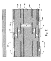
- FIG. 2 there is depicted a cross sectional view of a portion of a packaged integrated circuit, including an integrated circuit 15 and a package substrate 10 , depicting the separate transmitter routing layer 36 and receiver routing layer 44 .
- the layer 36 may be either the transmitter routing layer or the receiver routing layer, but in the preferred embodiment the transmitter routing layer is disposed above the receiver routing layer.
- references to layers being “upper” layers or “above” another layer have reference to layers that are closer to the integrated circuit 15 side of the package substrate 10
- references to layers being “lower” layers or “below” another layer have reference to layers that are farther from the integrated circuit 15 side of the package substrate 10 .
- a transmitter ground layer 34 and a transmitter power layer 38 Disposed on either side of the transmitter routing layer 36 are a transmitter ground layer 34 and a transmitter power layer 38 . It is appreciated that in alternate embodiments the transmitter ground layer could be below the transmitter routing layer and the transmitter power layer could be above the transmitter routing layer. However, in the preferred embodiment the transmitter ground layer 34 is disposed above the transmitter routing layer 36 , and the transmitter power layer 38 is disposed below the transmitter routing layer 36 , as depicted in FIG. 2 .
- a receiver ground layer 42 and a receiver power layer 46 disposed on either side of the receiver routing layer 44 . It is appreciated that in alternate embodiments the receiver ground layer could be below the receiver routing layer and the receiver power layer could be above the receiver routing layer. However, in the preferred embodiment the receiver ground layer 42 is disposed above the receiver routing layer 44 , and the receiver power layer 46 is disposed below the receiver routing layer 44 , as depicted in FIG. 2 .
- the various electrically conductive layers are disposed as described above, with electrically nonconductive layers disposed between them.
- the two additional layers 52 and 54 are preferably a second transmitter ground layer 52 and a second receiver ground layer 54 .
- the second transmitter ground layer 52 most preferably resides below the transmitter power layer 38 .
- the second receiver ground layer 54 most preferably resides below the receiver power layer 46 .
- the functions of the layers can be changed for an eight layer symmetric switching scenario, which is a specialized embodiment.
- the routing layer is bounded on either side by a ground layer, with a power layer disposed between one of the ground layers and the routing layer, while in the standard embodiment the routing layer is bounded on either side by a power layer, with a ground layer disposed adjacent one of the power layers.
- one of each of the two ground layers for the transmitter routing layer 36 and the receiver routing layer 44 is changed to a second power layer.
- FIG. 2 also depicts contact openings 30 in the upper solder mask layer 32 , where connections are made to the integrated circuit 15 .
- This comprises an upper contact layer, which is coplanar in this embodiment with the transmitter ground layer 34 .
- Contact openings 50 in the lower solder mask layer 48 provide connections to external circuitry.
- This comprises a lower contact layer, which is coplanar in this embodiment with the second receiver ground layer 54 .
- Electrically conductive vias 14 provide electrical connections from the contacts 30 and 50 on either side of the package substrate 10 through the various electrically nonconductive layers and between the various electrically conductive layers, as depicted.
- an electrically conductive ground layer of the package substrate 10 which may be either a transmitter ground layer 34 or a receiver ground layer 42 .
- the phantom blocks 12 a and 12 b depict a generalized projected location for the transceiver blocks 12 a and 12 b from the upper contact layer, and are provided for a reference.
- the ground layer tends to be a relatively large, unbroken conductive sheet. It is appreciated that there are preferably openings in the sheet for via contacts that must pass through the ground layer.
- the ground layer as described above, is electrically connected to the appropriate ground contacts in the transceiver pattern block 12 .
- FIG. 4 depicts a signal routing layer of the package substrate 10 , which may be either a transmitter routing layer 36 or a receiver routing layer 44 .
- the phantom blocks 12 a and 12 b depict a generalized projected location for the transceiver blocks 12 a and 12 b from the upper contact layer, and are provided for a reference.
- the signal routing layer includes transmitter signal traces 56 or receiver signal traces 58 , but not both.
- a routing layer includes one or the other type of signal traces, but not both, so that there is a greater degree of electrical isolation between the two different kinds of signal, be they transmitter or receiver.
- the signal traces 56 / 58 are preferably disposed in differential pairs, which are kept in close proximity one to another to improve the signal quality, where the spacing is preferably determined by the differential pair impedance that is required or desired.
- the signal traces 56 / 58 are connected to signal vias 20 / 24 , which are either transmitter signal vias 20 or receiver signal vias 24 , which are also disposed in differential pairs.
- the signal traces 56 / 58 route the signals to contacts 60 at the distal end of the differential pair of signal traces 56 / 58 .
- FIG. 5 depicts a power layer of the package substrate 10 , which may be either a transmitter power layer 38 or a receiver power layer 46 .
- the power layer 38 / 46 is preferably split into several power planes a-d, the purpose of which are described in more detail hereafter.
- the power planes a-d are electrically connected to the respective power contacts, either transmitter power contacts 18 or receiver power contacts 22 as appropriate in the transceiver array block 12 .
- the power planes 38 a-d are electrically connected to the transmitter power contacts 18 in the transceiver array 12 if the power layer is a transmitter power layer 38 .
- the power planes 46 a-d are electrically connected to the receiver power contacts 22 in the transceiver array 12 if the power layer is a receiver power layer 46 .
- FIG. 6 is a composite depiction of the power layer overlaid with the signal routing layer, to better illustrate how the power planes are associated with the signal routing traces. As depicted, only a single differential pair of signal traces 56 / 58 is associated with and is aligned with a given power plane 38 / 46 . In this manner, the signal traces 56 / 58 are provide with a relatively high degree of electrical isolation one from another, even while residing on the same routing layer.
- the association between power planes and signal traces is based on the transceiver block 12 .
- Signal traces that are electrically connected to transmitter or receiver contacts within a given transceiver block 12 are associated with and overlie power planes that are electrically connected to power contacts within the same transceiver block 12 .
- differential transmitter signal trace pairs 56 that are electrically connected to transmitter signal contacts 20 within a given transceiver block 12 a , are associated with and overlie a power plane 38 c that is electrically connected to transmitter power contacts 18 within the same transceiver block 12 a .
- differential receiver signal trace pairs 58 that are electrically connected to receiver signal contacts 24 within a given transceiver block 12 a , are associated with and overlie power plane 46 c that is electrically connected to receiver power contacts 22 within the same transceiver block 12 a .
- paired and dedicated power within a transceiver block is used within an isolation plane for associated signal traces.
- Lower electrical contacts 50 are disposed on the lower contact layer 46 and are electrically connected to the transmitter signal traces, the transmitter power planes, the transmitter ground layer, the receiver signal traces, the receiver power planes, and the receiver ground layer.
- a package substrate 10 according to the present invention provides isolation not only between transmitter signals and receiver signals, by placing them on separate routing layers, but also provides isolation between differential pairs of signal traces on the same layer, by sandwiching them between associated dedicated isolating power planes and common ground planes. In this manner, a very high speed transceiver core design can be used in a semi-custom package substrate design, which can accommodate a wide variety of different integrated circuit designs.
Abstract
Description
Claims (20)
Priority Applications (1)
| Application Number | Priority Date | Filing Date | Title |
|---|---|---|---|
| US10/615,063 US6744130B1 (en) | 2003-07-08 | 2003-07-08 | Isolated stripline structure |
Applications Claiming Priority (1)
| Application Number | Priority Date | Filing Date | Title |
|---|---|---|---|
| US10/615,063 US6744130B1 (en) | 2003-07-08 | 2003-07-08 | Isolated stripline structure |
Publications (1)
| Publication Number | Publication Date |
|---|---|
| US6744130B1 true US6744130B1 (en) | 2004-06-01 |
Family
ID=32326894
Family Applications (1)
| Application Number | Title | Priority Date | Filing Date |
|---|---|---|---|
| US10/615,063 Expired - Lifetime US6744130B1 (en) | 2003-07-08 | 2003-07-08 | Isolated stripline structure |
Country Status (1)
| Country | Link |
|---|---|
| US (1) | US6744130B1 (en) |
Cited By (8)
| Publication number | Priority date | Publication date | Assignee | Title |
|---|---|---|---|---|
| US20040216071A1 (en) * | 2003-04-22 | 2004-10-28 | Miller Leah M. | Routing structure for transceiver core |
| EP1631130A2 (en) * | 2004-08-30 | 2006-03-01 | Hirose Electric Co., Ltd. | Transmission circuit board |
| WO2017078717A1 (en) * | 2015-11-05 | 2017-05-11 | Intel Corporation | Stacked package assembly with voltage reference plane |
| CN108701684A (en) * | 2015-12-26 | 2018-10-23 | 英特尔公司 | The ground plane for being guided through the horizontal data signal transmission line of packaging is isolated vertically, ground path is coaxially isolated and impedance-tumed |
| US10194524B1 (en) * | 2017-07-26 | 2019-01-29 | Cisco Technology, Inc. | Anti-pad for signal and power vias in printed circuit board |
| US20190098765A1 (en) * | 2017-09-28 | 2019-03-28 | Juniper Networks, Inc. | Clearance size reduction for backdrilled differential vias |
| CN115767882A (en) * | 2023-01-09 | 2023-03-07 | 苏州浪潮智能科技有限公司 | Differential signal transmission circuit, circuit board, electronic device, and circuit manufacturing method |
| WO2023164078A1 (en) | 2022-02-25 | 2023-08-31 | E Ink Corporation | Electro-optic displays with edge seal components and methods of making the same |
Citations (3)
| Publication number | Priority date | Publication date | Assignee | Title |
|---|---|---|---|---|
| US5714801A (en) * | 1995-03-31 | 1998-02-03 | Kabushiki Kaisha Toshiba | Semiconductor package |
| US6184477B1 (en) * | 1998-12-02 | 2001-02-06 | Kyocera Corporation | Multi-layer circuit substrate having orthogonal grid ground and power planes |
| US6586828B2 (en) * | 2001-10-17 | 2003-07-01 | International Business Machines Corporation | Integrated circuit bus grid having wires with pre-selected variable widths |
-
2003
- 2003-07-08 US US10/615,063 patent/US6744130B1/en not_active Expired - Lifetime
Patent Citations (3)
| Publication number | Priority date | Publication date | Assignee | Title |
|---|---|---|---|---|
| US5714801A (en) * | 1995-03-31 | 1998-02-03 | Kabushiki Kaisha Toshiba | Semiconductor package |
| US6184477B1 (en) * | 1998-12-02 | 2001-02-06 | Kyocera Corporation | Multi-layer circuit substrate having orthogonal grid ground and power planes |
| US6586828B2 (en) * | 2001-10-17 | 2003-07-01 | International Business Machines Corporation | Integrated circuit bus grid having wires with pre-selected variable widths |
Cited By (16)
| Publication number | Priority date | Publication date | Assignee | Title |
|---|---|---|---|---|
| US7062742B2 (en) * | 2003-04-22 | 2006-06-13 | Lsi Logic Corporation | Routing structure for transceiver core |
| US20040216071A1 (en) * | 2003-04-22 | 2004-10-28 | Miller Leah M. | Routing structure for transceiver core |
| EP1631130A2 (en) * | 2004-08-30 | 2006-03-01 | Hirose Electric Co., Ltd. | Transmission circuit board |
| EP1631130A3 (en) * | 2004-08-30 | 2007-08-08 | Hirose Electric Co., Ltd. | Transmission circuit board |
| US10403604B2 (en) | 2015-11-05 | 2019-09-03 | Intel Corporation | Stacked package assembly with voltage reference plane |
| WO2017078717A1 (en) * | 2015-11-05 | 2017-05-11 | Intel Corporation | Stacked package assembly with voltage reference plane |
| CN108701684A (en) * | 2015-12-26 | 2018-10-23 | 英特尔公司 | The ground plane for being guided through the horizontal data signal transmission line of packaging is isolated vertically, ground path is coaxially isolated and impedance-tumed |
| US10580734B2 (en) * | 2015-12-26 | 2020-03-03 | Intel Corporation | Ground plane vertical isolation of, ground line coaxial isolation of, and impedance tuning of horizontal data signal transmission lines routed through package devices |
| US10194524B1 (en) * | 2017-07-26 | 2019-01-29 | Cisco Technology, Inc. | Anti-pad for signal and power vias in printed circuit board |
| CN109587942A (en) * | 2017-09-28 | 2019-04-05 | 瞻博网络公司 | Gap size for back-drilling formula difference through-hole reduces |
| US10470311B2 (en) * | 2017-09-28 | 2019-11-05 | Juniper Networks, Inc. | Clearance size reduction for backdrilled differential vias |
| US20190098765A1 (en) * | 2017-09-28 | 2019-03-28 | Juniper Networks, Inc. | Clearance size reduction for backdrilled differential vias |
| US10863628B2 (en) | 2017-09-28 | 2020-12-08 | Juniper Networks, Inc. | Clearance size reduction for backdrilled differential vias |
| CN109587942B (en) * | 2017-09-28 | 2022-03-08 | 瞻博网络公司 | Clearance size reduction for backdrilled differential vias |
| WO2023164078A1 (en) | 2022-02-25 | 2023-08-31 | E Ink Corporation | Electro-optic displays with edge seal components and methods of making the same |
| CN115767882A (en) * | 2023-01-09 | 2023-03-07 | 苏州浪潮智能科技有限公司 | Differential signal transmission circuit, circuit board, electronic device, and circuit manufacturing method |
Similar Documents
| Publication | Publication Date | Title |
|---|---|---|
| US5847936A (en) | Optimized routing scheme for an integrated circuit/printed circuit board | |
| US6388890B1 (en) | Technique for reducing the number of layers in a multilayer circuit board | |
| US7256354B2 (en) | Technique for reducing the number of layers in a multilayer circuit board | |
| US6011695A (en) | External bus interface printed circuit board routing for a ball grid array integrated circuit package | |
| WO1984002631A1 (en) | Semiconductor chip package | |
| JP2005515611A (en) | High performance low cost micro circuit package with interposer | |
| US7095107B2 (en) | Ball assignment schemes for integrated circuit packages | |
| US7062742B2 (en) | Routing structure for transceiver core | |
| US20020038724A1 (en) | Chip scale package, printed circuit board, and method of designing a piinted circuit board | |
| US6664620B2 (en) | Integrated circuit die and/or package having a variable pitch contact array for maximization of number of signal lines per routing layer | |
| EP1361612B1 (en) | Organic substrate for flip chip bonding | |
| US6744130B1 (en) | Isolated stripline structure | |
| US20050109535A1 (en) | High performance chip carrier substrate | |
| US20010008313A1 (en) | Chip package with degassing holes | |
| CN100525578C (en) | Method for increasing a routing density for a circuit board and such a circuit board | |
| US5914533A (en) | Multilayer module with thinfilm redistribution area | |
| CN1327519C (en) | Device package, a printed wiring board, and an electronic apparatus | |
| US5691569A (en) | Integrated circuit package that has a plurality of staggered pins | |
| CN110911384A (en) | Embedded passive bridge chip and application thereof | |
| JPH0239101B2 (en) | ||
| US6479319B1 (en) | Contact escape pattern | |
| US7105926B2 (en) | Routing scheme for differential pairs in flip chip substrates | |
| US20090174072A1 (en) | Semiconductor system having bga package with radially ball-depopulated substrate zones and board with radial via zones | |
| KR20040057895A (en) | Technique for electrically interconnecting electrical signals between an electronic component and a multilayer signal routing device | |
| KR100505672B1 (en) | Array printed circuit board having symmetric layout |
Legal Events
| Date | Code | Title | Description |
|---|---|---|---|
| AS | Assignment |
Owner name: LSI LOGIC CORPORATION, CALIFORNIA Free format text: ASSIGNMENT OF ASSIGNORS INTEREST;ASSIGNORS:MILLER, LEAH M.;THURAIRAJARATNAM, ARITHARAN;FULCHER, EDWIN M.;REEL/FRAME:014298/0534;SIGNING DATES FROM 20030630 TO 20030707 |
|
| STCF | Information on status: patent grant |
Free format text: PATENTED CASE |
|
| FPAY | Fee payment |
Year of fee payment: 4 |
|
| FEPP | Fee payment procedure |
Free format text: PAYOR NUMBER ASSIGNED (ORIGINAL EVENT CODE: ASPN); ENTITY STATUS OF PATENT OWNER: LARGE ENTITY |
|
| FPAY | Fee payment |
Year of fee payment: 8 |
|
| AS | Assignment |
Owner name: DEUTSCHE BANK AG NEW YORK BRANCH, AS COLLATERAL AG Free format text: PATENT SECURITY AGREEMENT;ASSIGNORS:LSI CORPORATION;AGERE SYSTEMS LLC;REEL/FRAME:032856/0031 Effective date: 20140506 |
|
| AS | Assignment |
Owner name: LSI CORPORATION, CALIFORNIA Free format text: CHANGE OF NAME;ASSIGNOR:LSI LOGIC CORPORATION;REEL/FRAME:033102/0270 Effective date: 20070406 |
|
| AS | Assignment |
Owner name: AVAGO TECHNOLOGIES GENERAL IP (SINGAPORE) PTE. LTD Free format text: ASSIGNMENT OF ASSIGNORS INTEREST;ASSIGNOR:LSI CORPORATION;REEL/FRAME:035390/0388 Effective date: 20140814 |
|
| FPAY | Fee payment |
Year of fee payment: 12 |
|
| AS | Assignment |
Owner name: LSI CORPORATION, CALIFORNIA Free format text: TERMINATION AND RELEASE OF SECURITY INTEREST IN PATENT RIGHTS (RELEASES RF 032856-0031);ASSIGNOR:DEUTSCHE BANK AG NEW YORK BRANCH, AS COLLATERAL AGENT;REEL/FRAME:037684/0039 Effective date: 20160201 Owner name: AGERE SYSTEMS LLC, PENNSYLVANIA Free format text: TERMINATION AND RELEASE OF SECURITY INTEREST IN PATENT RIGHTS (RELEASES RF 032856-0031);ASSIGNOR:DEUTSCHE BANK AG NEW YORK BRANCH, AS COLLATERAL AGENT;REEL/FRAME:037684/0039 Effective date: 20160201 |
|
| AS | Assignment |
Owner name: BANK OF AMERICA, N.A., AS COLLATERAL AGENT, NORTH CAROLINA Free format text: PATENT SECURITY AGREEMENT;ASSIGNOR:AVAGO TECHNOLOGIES GENERAL IP (SINGAPORE) PTE. LTD.;REEL/FRAME:037808/0001 Effective date: 20160201 Owner name: BANK OF AMERICA, N.A., AS COLLATERAL AGENT, NORTH Free format text: PATENT SECURITY AGREEMENT;ASSIGNOR:AVAGO TECHNOLOGIES GENERAL IP (SINGAPORE) PTE. LTD.;REEL/FRAME:037808/0001 Effective date: 20160201 |
|
| AS | Assignment |
Owner name: AVAGO TECHNOLOGIES GENERAL IP (SINGAPORE) PTE. LTD., SINGAPORE Free format text: TERMINATION AND RELEASE OF SECURITY INTEREST IN PATENTS;ASSIGNOR:BANK OF AMERICA, N.A., AS COLLATERAL AGENT;REEL/FRAME:041710/0001 Effective date: 20170119 Owner name: AVAGO TECHNOLOGIES GENERAL IP (SINGAPORE) PTE. LTD Free format text: TERMINATION AND RELEASE OF SECURITY INTEREST IN PATENTS;ASSIGNOR:BANK OF AMERICA, N.A., AS COLLATERAL AGENT;REEL/FRAME:041710/0001 Effective date: 20170119 |
|
| AS | Assignment |
Owner name: BELL SEMICONDUCTOR, LLC, ILLINOIS Free format text: ASSIGNMENT OF ASSIGNORS INTEREST;ASSIGNORS:AVAGO TECHNOLOGIES GENERAL IP (SINGAPORE) PTE. LTD.;BROADCOM CORPORATION;REEL/FRAME:044886/0766 Effective date: 20171208 |
|
| AS | Assignment |
Owner name: CORTLAND CAPITAL MARKET SERVICES LLC, AS COLLATERA Free format text: SECURITY INTEREST;ASSIGNORS:HILCO PATENT ACQUISITION 56, LLC;BELL SEMICONDUCTOR, LLC;BELL NORTHERN RESEARCH, LLC;REEL/FRAME:045216/0020 Effective date: 20180124 |
|
| AS | Assignment |
Owner name: BELL NORTHERN RESEARCH, LLC, ILLINOIS Free format text: RELEASE BY SECURED PARTY;ASSIGNOR:CORTLAND CAPITAL MARKET SERVICES LLC;REEL/FRAME:059723/0382 Effective date: 20220401 Owner name: BELL SEMICONDUCTOR, LLC, ILLINOIS Free format text: RELEASE BY SECURED PARTY;ASSIGNOR:CORTLAND CAPITAL MARKET SERVICES LLC;REEL/FRAME:059723/0382 Effective date: 20220401 Owner name: HILCO PATENT ACQUISITION 56, LLC, ILLINOIS Free format text: RELEASE BY SECURED PARTY;ASSIGNOR:CORTLAND CAPITAL MARKET SERVICES LLC;REEL/FRAME:059723/0382 Effective date: 20220401 |