US6777149B2 - Electrophotographic image forming apparatus and process cartridge, and electrophotographic photoreceptor therefor - Google Patents

Electrophotographic image forming apparatus and process cartridge, and electrophotographic photoreceptor therefor Download PDF

Info

Publication number
US6777149B2
US6777149B2 US10/104,078 US10407802A US6777149B2 US 6777149 B2 US6777149 B2 US 6777149B2 US 10407802 A US10407802 A US 10407802A US 6777149 B2 US6777149 B2 US 6777149B2
Authority
US
United States
Prior art keywords
group
substituted
ring
unsubstituted
charge generation
Prior art date
Legal status (The legal status is an assumption and is not a legal conclusion. Google has not performed a legal analysis and makes no representation as to the accuracy of the status listed.)
Expired - Lifetime
Application number
US10/104,078
Other versions
US20030059693A1 (en
Inventor
Takaaki Ikegami
Akihiro Sugino
Current Assignee (The listed assignees may be inaccurate. Google has not performed a legal analysis and makes no representation or warranty as to the accuracy of the list.)
Ricoh Co Ltd
Original Assignee
Ricoh Co Ltd
Priority date (The priority date is an assumption and is not a legal conclusion. Google has not performed a legal analysis and makes no representation as to the accuracy of the date listed.)
Filing date
Publication date
Application filed by Ricoh Co Ltd filed Critical Ricoh Co Ltd
Assigned to RICOH COMPANY LIMITED reassignment RICOH COMPANY LIMITED ASSIGNMENT OF ASSIGNORS INTEREST (SEE DOCUMENT FOR DETAILS). Assignors: IKEGAMI, TAKAAKI, SUGINO, AKIHIRO
Publication of US20030059693A1 publication Critical patent/US20030059693A1/en
Application granted granted Critical
Publication of US6777149B2 publication Critical patent/US6777149B2/en
Anticipated expiration legal-status Critical
Expired - Lifetime legal-status Critical Current

Links

Images

Classifications

    • GPHYSICS
    • G03PHOTOGRAPHY; CINEMATOGRAPHY; ANALOGOUS TECHNIQUES USING WAVES OTHER THAN OPTICAL WAVES; ELECTROGRAPHY; HOLOGRAPHY
    • G03GELECTROGRAPHY; ELECTROPHOTOGRAPHY; MAGNETOGRAPHY
    • G03G5/00Recording members for original recording by exposure, e.g. to light, to heat, to electrons; Manufacture thereof; Selection of materials therefor
    • G03G5/02Charge-receiving layers
    • G03G5/04Photoconductive layers; Charge-generation layers or charge-transporting layers; Additives therefor; Binders therefor
    • G03G5/06Photoconductive layers; Charge-generation layers or charge-transporting layers; Additives therefor; Binders therefor characterised by the photoconductive material being organic
    • G03G5/0664Dyes
    • G03G5/0675Azo dyes
    • G03G5/0679Disazo dyes
    • GPHYSICS
    • G03PHOTOGRAPHY; CINEMATOGRAPHY; ANALOGOUS TECHNIQUES USING WAVES OTHER THAN OPTICAL WAVES; ELECTROGRAPHY; HOLOGRAPHY
    • G03GELECTROGRAPHY; ELECTROPHOTOGRAPHY; MAGNETOGRAPHY
    • G03G5/00Recording members for original recording by exposure, e.g. to light, to heat, to electrons; Manufacture thereof; Selection of materials therefor
    • G03G5/02Charge-receiving layers
    • G03G5/04Photoconductive layers; Charge-generation layers or charge-transporting layers; Additives therefor; Binders therefor
    • G03G5/043Photoconductive layers characterised by having two or more layers or characterised by their composite structure
    • G03G5/047Photoconductive layers characterised by having two or more layers or characterised by their composite structure characterised by the charge-generation layers or charge transport layers
    • GPHYSICS
    • G03PHOTOGRAPHY; CINEMATOGRAPHY; ANALOGOUS TECHNIQUES USING WAVES OTHER THAN OPTICAL WAVES; ELECTROGRAPHY; HOLOGRAPHY
    • G03GELECTROGRAPHY; ELECTROPHOTOGRAPHY; MAGNETOGRAPHY
    • G03G5/00Recording members for original recording by exposure, e.g. to light, to heat, to electrons; Manufacture thereof; Selection of materials therefor
    • G03G5/14Inert intermediate or cover layers for charge-receiving layers

Definitions

  • the present invention relates to an electrophotographic image forming apparatus and a process cartridge as well as an electrophotographic photoreceptor used for copiers and printers using coherent light as the light sources.
  • a printer having a laser diode as the light source is widely used because of its compactness, high reliability, high-speed printing and high image quality.
  • a photoreceptor which is sensitive to infrared light is desired because the laser diode has a wavelength of from 780 to 830 nm.
  • inorganic photoreceptors formed from cadmium sulfide doped with copper, indium, etc. and from selenium including increased tellurium have been used.
  • organic photoreceptors are prevailing recently in view of the low pollution high productivity, stable quality and low cost.
  • the organic photoreceptors particularly a functionally-separated multilayer photoreceptor having a charge generation layer and a charge transport layer attracts attention in view of the high sensitivity and high durability because the materials can be flexibly selected.
  • the charge generation layer of the multilayer photoreceptor generates a charge by absorbing light, and the thickness of the layer is typically 0.01 to 5 ⁇ m for shortening the carrying range of the photo-carrier to prevent the recombination and the trap thereof.
  • a charge transport layer which scarcely absorbs imagewise light is typically used in view of the sensitivity.
  • the light volume which is absorbed in the photosensitive layer has a limit.
  • the imagewise light coming in the photosensitive layer is not all absorbed therein, and some of the light reach the substrate and reflect on the surface thereof.
  • the reflected light comes in the photosensitive layer again, and interferes with the imagewise light and the light reflecting on the surface of the photosensitive layer.
  • Such a phenomenon remarkably occurs when the imagewise light is a coherent laser beam, causing image-density irregularity when a solid image and a half tone image are produced.
  • an intermediate layer including a resin containing a dispersed pigment having a large refraction index and an average particle diameter of from about 0.2 ⁇ m to 5 ⁇ m, is formed between the substrate and the photosensitive layer to scatter the light and prevent the mirror reflection.
  • an intermediate layer cannot completely prevent the light interference when the imagewise light volume and the developing condition change, and when a minimization of the diameter of the imagewise light and a high-density writing are desired for a higher image quality
  • a non-cut aluminium tube is considered instead of a conventional cut aluminium tube recently in view of the manufacturing cost and the adherence to the photosensitive layer.
  • the non-cut aluminium tube has a surface having a high smoothness and a high reflectance, and has the opposite effect to the light interference.
  • an object of the present invention is to provide an electrophotographic image forming apparatus preventing the image-density irregularity due to the light interference.
  • an image forming apparatus including at least an image irradiator configured to irradiate a photoreceptor with a coherent light beam while scanning to form pixel light spots thereon for forming an electrostatic latent image thereon, wherein the light spots overlap with adjacent light spots; and an image developer configured to develop the electrostatic latent image with a developer, wherein the photoreceptor comprises an intermediate layer located overlying an electroconductive substrate, a charge generation layer located overlying the intermediate layer and a charge transport layer located overlying the charge generation layer, wherein the charge generation layer satisfies the following relationship:
  • T1 represents a relative mirror reflectance of the charge generation layer against the coherent light beam when the coherent light beam irradiates the charge generation layer formed on the intermediate layer at an incident angle of 5°.
  • FIG. 1 is a schematic view illustrating a relationship between the coherent light spots
  • FIG. 2 is a graph showing a relationship between a coherent light beam and an adjacent coherent light beam
  • FIG. 3 is a measuring principle of the relative mirror reflectance
  • FIG. 4 is a schematic view of an embodiment of the electrophotographic process of the present invention.
  • FIG. 5 is a schematic view of another embodiment of the electrophotographic process of the present invention.
  • FIG. 6 is a schematic view of an embodiment of the process cartridge of the present invention.
  • the present invention provides an electrophotographic image forming apparatus preventing the image-density irregularity due to the light interference.
  • an image irradiation is performed by irradiating coherent light, in which an interval between a coherent light spot and an adjacent coherent light spot is smaller than the diameter of the coherent light, namely there is an overlapped portion between the coherent light spot and the adjacent coherent light spot.
  • the present inventors found that the overlapped portion is a cause of the image-density irregularity in case of the above-mentioned irradiation. Particularly, when the overlapped area becomes large in proportion to high image resolution, the inventors found that the light interference affects the image-density irregularity far more than considered.
  • the image-density irregularity due to the light interference in the photoreceptor including an intermediate layer between the substrate and the photosensitive layer occurs when the relative mirror reflectance of the charge generation layer against the coherent light when the coherent light irradiates the charge generation layer formed on the intermediate layer at an incident angle of 5°is greater than 3.5%, and that the image-density irregularity can be prevented when the relative mirror reflectance is not greater than 3.5%.
  • T1 represents a relative mirror reflectance of the charge generation layer
  • T2 represents a relative mirror reflectance against the coherent light when the coherent light irradiates the intermediate layer at an incident angle of 5°.
  • a photoreceptor having the relative mirror reflectance of the present invention is particularly effective for an electrophotographic device in which the diameter of the pixel light spots is not greater than 40 ⁇ m and the overlapped area is not less than 50% of the area of each of the light spot.
  • the diameter of the pixel light spots is preferably not greater than 25 ⁇ m.
  • FIG. 1 is a schematic view illustrating a relationship between the coherent light spots
  • FIG. 2 is a graph showing a relationship between a coherent light beam and an adjacent coherent light beam.
  • the intervals (a and a′) between the coherent light spots is determined depending on the density (writing resolution) of a latent image formed by the coherent light.
  • the coherent light diameter (d and d′) is defined as an area in which the light energy is ⁇ /e 2 or more when ⁇ is a peak energy of the coherent light having a Gauss distribution.
  • the relative mirror reflectance against the coherent light having an incident angle of 5° can be typically measured by a measuring device based on the measuring principle as shown in FIG. 3 .
  • An aluminium-deposited mirror having a stable spectral reflectance is preferably used as a reflection standard.
  • T1 is preferably not greater than 3.0%, and more preferably not greater than 2.5%.
  • T2 is preferably not greater than 3.5%, and more preferably not greater than 3.0%.
  • the intermediate layer of the present invention preferably includes a resin containing a dispersed pigment having a large refractive index.
  • Known pigment powders can be used for the dispersed pigment particulate powder.
  • white powders or others which are similar thereto are preferable in consideration of the high sensitivity of the resultant photoreceptor.
  • Specific examples of such powders include metal oxides such as titanium oxide, zinc oxide, tin oxide, indium oxide, zirconium oxide, alumina and silica. These are preferably used because they are not hygroscopic and do not change much in quality due to change of the environment.
  • the titanium oxide having a good refractive index and electrical properties is preferably used.
  • a binder resin for the intermediate layer of the present invention appropriate resins can be used.
  • a resin having a high solvent resistance against general organic solvents is preferably used because a photosensitive layer is coated on the intermediate layer.
  • resins include water-soluble resins such as polyvinylalcohol, casein and sodium polyacrylate; alcohol-soluble resins such as nylon copolymers and methoxymethylated nylon; and curing resins forming a 3-dimensional network structure such as polyurethane resins, melamine resins and epoxy resins.
  • the intermediate layer preferably has a thickness of from 0.5 to 50 ⁇ m, and more preferably from 1.0 to 20 ⁇ m.
  • the volume ratio of the powder (P) and the binder resin (R), i.e., P/R of the intermediate layer is preferably from 1/1 to 3/1.
  • P/R binder resin
  • the properties of the intermediate layer tend to depend on the properties of the resin.
  • the P/R is greater than 3/1, the intermediate layer has many empty spaces therein and air bubbles tend to generate in the photosensitive layer formed thereon.
  • the relative mirror reflectance T2 of the present invention changes in accordance with the pigment.
  • T2 can be also controlled by the dispersed condition of the pigment, and the affinity and mixing ratio of the pigment and the binder resin.
  • a pigment which is sensitive to a long wavelength can be used.
  • phthalocyanine pigments such as metallic phthalocyanine and metal-free phthalocyanine, azulenium salt pigments, Squarilium salt pigments and azo pigments can be used.
  • the relative mirror reflectance T1 can be preferably obtained by using a disazo pigment having the following formula (I).
  • a coupler residual group having the formula (II) can be preferably used in respect of sensitivity of the resultant photoreceptor.
  • a and B independently represent a coupler residual
  • X 1 represents —OH, —NHCOCH 3 or —NHSO 2 CH 3 ;
  • Y 1 represents —CON(R 2 )(R 3 ), —CONHN ⁇ C(R 6 )(R 7 ), —CONHN (R 8 )(R 9 ), —CONHCONH(R 12 ), a hydrogen atom, —COOH, —COOCH 3 , COOC 6 H 5 or a benzimidazolyl group,
  • R 2 and R 3 independently represent a hydrogen atom, a substituted or unsubstituted alkyl group, a substituted or unsubstituted aryl group and a substituted or unsubstituted hetero ring group; R 2 and R 3 optionally form a ring together with a nitrogen atom; R 6 and R 7 independently represent a hydrogen atom, a substituted or unsubstituted alkyl group, a substituted or unsubstituted aralkyl group, a substituted or unsubstituted aryl group, a substituted or unsubstituted styryl group and a substituted or unsubstituted hetero ring group; R 6 and R 7 optionally form a ring together with a carbon atom; R 8 and R 9 independently represent a hydrogen atom, a substituted or unsubstituted alkyl group, a substituted or unsubstituted aralkyl group, a substituted or unsubstit
  • R 4 represents a hydrogen atom, a substituted or unsubstituted alkyl group, or a substituted or unsubstituted aryl group;
  • R 5 represents a hydrogen atom, a substituted or unsubstituted alkyl group, or a substituted or unsubstituted aryl group;
  • Y represents a divalent aromatic hydrocarbon group or a divalent hetero ring including a nitrogen atom in the ring;
  • Y represents a divalent aromatic hydrocarbon group or a divalent hetero ring including a nitrogen atom in the ring;
  • R 10 represents a hydrogen atom, a lower alkyl group having 1 to 6 carbon atoms, a carboxyl group or an ester of a carboxyl group; and Ar 1 represents a substituted or unsubstituted aromatic hydrocarbon ring group; and
  • R 10 represents a hydrogen atom, a lower alkyl group having 1 to 6 carbon atoms, a carboxyl group or an ester of a carboxyl group; and Ar 1 represents a substituted or unsubstituted aromatic hydrocarbon ring group.
  • alkyl group means a saturated hydrocarbyl group having from 1 to 16 carbons, preferably from 1 to 11 carbons.
  • Preferred alkyl groups include, but are not limited to methyl, ethyl, propyl, butyl, pentyl, hexyl, heptyl, octyl, nonyl, decyl, and undecyl groups, either linear or branched. More preferred are methyl, ethyl, propyl, butyl, hexyl and undecyl.
  • aryl group means mono to hexavalent aromatic hydrocarbon groups made of aromatic hydrocarbon rings, preferably including but not limited to, phenyl, naphthyl, anthracenyl and pyrenyl, which may be unsubstited or substituted.
  • aralkyl group means a combination of one of the above mentioned aryl groups and one of the above mentioned alkyl groups, wherein the group is preferably attached to the molecule core through the alkyl portion of the group.
  • hetero ring group means mono-to-hexavalent aromatic heterocyclic groups having one or more aromatic heterocyclic rings.
  • the aromatic heterocyclic rings include, but are not limited to, pyridinyl, quinolinyl, thiophenyl, furyl, oxazolyl, oxadiazolyl and carbazolyl, wherein the heterocyclic ring may be substituted or unsubtituted.
  • the substituents can be selected from any substituent that does not interfere with the charge generation properties of the compound.
  • the substituent includes, but is not limited to, one or more groups independently selected from alkyl having 1 to 16 carbons, alkoxy groups having 1 to 16 carbons, halogen groups and aryl groups as defined above. More preferably, the substituent(s) include one or more groups independently selected from methyl, ethyl, propyl, butyl, hexyl, undecyl, methoxy, ethoxy, propoxy, butoxy, fluoro, chloro, bromo, iodo and the above noted aryl groups.
  • Couplers forming a coupler residual group of the disazo pigments having the formula (I) are shown in Tables 1 to 16.
  • Coupler No. (R)n Melting Point (° C.) 133 H >300 134 2-OCH 3 268 135 3-OCH 3 281.0 to 283.0 136 4-OCH 3 293 137 2-CH 3 297 138 3-CH 3 296 139 4-CH 3 >300 140 4-Cl >300 141 2-NO 2 >300 142 4-NO 2 >300 143 2-OH >300 144 2-OH, 3-NO 2 >300 145 2-OH, 5-NO 2 >300 146 2-OH, 3-OCH 3 >300
  • Coupler No. (R 2 )n 262 4-CH 3 263 3-NO 2 264 2-Cl 265 3-Cl 266 4-Cl 267 2-Cl, 3-Cl 268 2-Cl, 4-Cl 269 3-Cl, 5-Cl 270 2-Cl, 5-Cl 271 3-Cl, 4-Cl
  • the charge generation layer can be formed by the following method:
  • the above-mentioned charge generation materials are dispersed in a liquid solution of a binder resin such as polyester resins, polycarbonate resins, polyvinylbutyral resins and acrylic resins by a ball mill, an attritor, a sand mill, etc; and
  • a binder resin such as polyester resins, polycarbonate resins, polyvinylbutyral resins and acrylic resins
  • the dispersed liquid is properly diluted and coated on a substrate by a dip coating, a spray coating, a bead coating method, etc.
  • the relative mirror reflectance T1 of the present invention changes in accordance with the charge generation material.
  • T1 can be also controlled by the dispersed condition of the charge generation material, and the affinity and mixing ratio of the pigment and the binder resin as well as the composition of the above-mentioned intermediate layer.
  • the charge generation layer preferably has a thickness of from 0.01 to 5 ⁇ m, and more preferably from 0.1 to 2 ⁇ m.
  • the charge transport layer is formed from a charge transport material and a binder resin which is optionally used.
  • the material is dissolved or dispersed in a proper solvent, and the liquid solution is coated on a substrate and dried to form the charge transport layer.
  • the charge transport materials there are a hole transport material and an electron transport material.
  • the hole transport materials include electron imparting materials such as poly-N-vinylcarbazole and its derivatives, poly- ⁇ -carbazolylethylgultamate and its derivatives, pyrene-formaldehyde condensates and their derivatives, polyvinylpyrene, polyvinylphenanthrene, oxazole derivatives, oxadiazole derivatives, imidazole derivatives, triphenylamine derivatives, 9-(P-diethylaminostyryl)anthracene, 1,1-bis-(4-dibenzylaminophenyl)propane, styrylanthracene, styrylpyrazoline, phenylhydrazone compounds and ⁇ -phenylstilbene derivatives.
  • electron imparting materials such as poly-N-vinylcarbazole and its derivatives, poly- ⁇ -carbazolylethylgultamate and its derivatives, pyrene-formaldeh
  • the electron transport materials include electron accepting materials such as chloranil, bromoanil, tetracyanoethylene, tetracyanoquinodimethane, 2,4,7-trinitro-9-fluorenone, 2,4,5,7-tetranitro-9-fluorenone, 2,4,5,7-tetranitroxanthone, 2,4,8-trinitrothioxanthone, 2,6,8-trinitro-indeno [1,2-b] thiophene-4-one and 1,3,7-trinitrodibenzothiophene-5,5-dioxide.
  • electron accepting materials such as chloranil, bromoanil, tetracyanoethylene, tetracyanoquinodimethane, 2,4,7-trinitro-9-fluorenone, 2,4,5,7-tetranitro-9-fluorenone, 2,4,5,7-tetranitroxanthone, 2,4,8-trinitrothioxanthone, 2,6,8-trinitro-indeno [1,2-b] thioph
  • binder resins for optional use in the present invention include thermoplastic or thermosetting resins such as polystyrene resins, styrene-acrylonitrile copolymers, styrene-butadiene copolymers, styrene-maleic anhydride copolymers, polyester resins, polyvinyl chloride resins, vinyl chloride-vinyl acetate copolymers, polyvinyl acetate resins, polyvinylidene chloride resins, polyarylate resins, polycarbonate resins, cellulose acetate resins, ethyl cellulose resins, polyvinyl butyral resins, polyvinyl formal resins, polyvinyl toluene resins, poly-N-vinylcarbazole resins, acrylic resins, silicone resins, epoxy resins, melamine resins, urethane resins, phenol resins and alkyd resins.
  • thermoplastic or thermosetting resins such as polystyren
  • solvents include tetrahydrofuran, dioxane, toluene, monochlorobenzene, dichloroethane, methylene chloride, etc.
  • the charge transport layer preferably has a thickness of from 5 to 100 ⁇ /m.
  • a plasticizer and a leveling agent can be included in the charge transport layer of the present invention.
  • the plasticizer conventional plasticizers for resins, such as dibutylphthalate and dioctylphthalate can be used.
  • the content of the plasticizer is preferably from 0 to 30% by weight per 100% by weight of the binder resin.
  • the leveling agent silicone oils such as dimethyl silicone oils and methyl phenyl silicone oils can be used.
  • the content of the leveling agent is preferably from 0 to 1% by weight per 100% by weight of the binder resin.
  • an insulating layer and a protective layer can be formed on the photosensitive layer in the present invention.
  • the substrate used for the photoreceptor of the present invention is formed as follows. Metals such as aluminium and nickel are deposited or laminated on metallic drums and sheets such as aluminium, brass, stainless and nickel; polyethyleneterephthalate; polypropylene; nylon; paper, etc. Among the substrates, a cylindrical drum formed of aluminium or its alloyed metals is widely used at present. Particularly, non-cut aluminium tube without a cutting process is preferably used because the manufacturing cost is lower and the adherence to the photosensitive layer is higher than that of a conventional cut aluminium tube.
  • the photoreceptor having the relative mirror reflectance of the present invention can prevent image-density irregularity of the resultant image even if the non-cut aluminium tube is used for the substrate.
  • Such aluminium alloys are formed by the method disclosed in JIS3003, 5000, 6000, etc. and the non-cut aluminium tube is formed by a conventional method such as EI, ED, DI and II methods.
  • FIG. 4 is a schematic view for explaining the electrophotographic process and device of the present invention, and the following modified example also belongs to the present invention.
  • a photoreceptor 1 includes a drum substrate on which a photosensitive layer is formed.
  • a charger 3 a pre-transfer charger 7 , a transfer charger 10 , a separation charger 11 and a pre-cleaning charger 13 , known chargers such as corotrons, scorotrons, solid state chargers and charging rollers are used.
  • the transfer means the above-mentioned chargers can be used, however, a combination of a transfer charger 10 and a separation charger 11 as shown in FIG. 4 is effectively used.
  • coherent light such as light emitting diodes (LEDS), laser diode (LDs) and electroluminescence (EL) lamps is used.
  • LEDS light emitting diodes
  • LDs laser diode
  • EL electroluminescence
  • any known illuminators such as fluorescent lamps, tungsten lamps, halogen lamps, mercury lamps, sodium lamps, light emitting diodes (LEDs), laser diodes (LDs) and electro luminescense (EL) lamps can be used.
  • various filters such as sharp cut filters, band pass filters, near infrared cutting filters, dichroic filters, interference filters and conversion filters can be also used.
  • Such light sources can be also used for irradiating the photoreceptor in processes such as a transfer process combined with light irradiation, a charge eliminating process, a cleaning process, a pre-exposure process, etc. as well as the processes mentioned above.
  • Toner images formed on the photoreceptor 1 by developing unit 6 are transferred on a transfer paper 9 . However, all of the toner particles of the toner images are not transferred on the transfer paper 9 and there also remain toner particles on the photoreceptor 1 . Such toner particles are removed from photoreceptors by a fur brush 14 and a blade 15 . Cleaning may be made only by a known cleaning brush such as fur brushes and mag-fur brushes.
  • FIG. 5 shows another embodiment of the electrophotographic process of the present invention.
  • a photoreceptor 21 has the photosensitive layer of the present invention, and is driven by driving rollers 22 a and 22 b .
  • the photoreceptor 21 is charged by a charger 23 , and exposed to light emitted by a light source 24 to form a latent image thereon.
  • the latent image is developed by an image developer (not illustrated) to form a toner image thereon.
  • the toner image is transferred on a transfer paper (not shown) using a charger 25 .
  • the photoreceptor 21 is then subjected to a cleaning pre-exposure treatment using a light source 26 , a cleaning treatment using a brush 27 and a discharging treatment using a light source 28 . These processes are repeatedly performed to produce images.
  • pre-cleaning light irradiates the photoreceptor 21 from the substrate side. (In this case, the substrate is transparent.)
  • the cleaning pre-exposure is made from the substrate side
  • the cleaning pre-exposure may be made from the photosensitive layer side.
  • irradiation of image exposure and discharging can be made from the substrate side.
  • the image exposure, cleaning pre-exposure and discharging exposure are illustrated.
  • light irradiation such as pre-transfer exposure, pre-exposure of image exposure and other known light irradiation processes can be made to the photoreceptors.
  • the electrophotographic device as mentioned above can be fixedly installed into copiers, facsimiles and printers. In addition, they can be installed into these devices in the form of a process cartridge as well.
  • the process cartridge is a device (part) containing at least a photoreceptor, and at least one of a charger, an image irradiator, an image developer, an image transfer, a cleaner and a discharger.
  • FIG. 6 is a schematic view illustrating an embodiment of the process cartridge of the present invention.
  • a photoreceptor 16 has a photosensitive layer of the present invention.
  • a polyvinylbutyral resin 1 (S-LEC BM-S from Sekisui Chemical Co., Ltd.) Cyclohexanone 250
  • a polyvinylbutyral resin 1 (XYHL from Union Carbide Corp.) Cyclohexanone 250
  • A-type titanylphthalocyanine 5 A polyvinylbutyral resin 5 (S-LEC BM-S from Sekisui Chemical Co., LTD.) Methyl ethyl ketone 350
  • A-type titanylphthalocyanine 5 A disazo pigment 5
  • a polyvinylbutyral resin 5 (S-LEC BM-S from Sekisui Chemical Co., LTD.) Cyclohexanone 250
  • each coating liquid was coated on a non-cut aluminium tube formed by an ED method, having an outer diameter of 30 mm and a length of 340 mm.
  • a coating liquid for a charge transport layer having the following components was further coated on each coated tube, and dried to form a charge transport layer having a thickness of 20 ⁇ m.
  • each process cartridge was installed in the following electrophotographic processes A to E shown in FIG. 4 .
  • Wavelength of light source for Diameter of image image irradiator writing light beam Light spot interval/ (LD) by a polygon mirror overlapped area
  • Example 9 and Comparative Example 15 durability test for Example 9 and Comparative Example 15 was performed by producing continuous 50,000 images. It was observed that the end of the photosensitive layer of the photoreceptor of Example 15 was partly peeled off, and that the non-cut aluminium tube used in Example 9 had higher adherence to the photosensitive layer than that of Example 15.

Abstract

An image forming apparatus including at least an image irradiator configured to irradiate a photoreceptor with a coherent light beam while scanning to form pixel light spots thereon for forming an electrostatic latent image thereon, wherein the light spots overlap with adjacent light spots; and an image developer configured to develop the electrostatic latent image with a developer, wherein the photoreceptor comprises an intermediate layer located overlying an electroconductive substrate, a charge generation layer located overlying the intermediate layer and a charge transport layer located overlying the charge generation layer, wherein the charge generation layer satisfies the following relationship:
T1≦3.5%
wherein T1 represents a relative mirror reflectance of the charge generation layer against the coherent light beam when the coherent light beam irradiates the charge generation layer at an incident angle of 5°.

Description

BACKGROUND OF THE INVENTION
1. Field of the Invention
The present invention relates to an electrophotographic image forming apparatus and a process cartridge as well as an electrophotographic photoreceptor used for copiers and printers using coherent light as the light sources.
2. Discussion of the Background
Recently, a printer having a laser diode as the light source is widely used because of its compactness, high reliability, high-speed printing and high image quality. However, a photoreceptor which is sensitive to infrared light is desired because the laser diode has a wavelength of from 780 to 830 nm. As such photoreceptors, inorganic photoreceptors formed from cadmium sulfide doped with copper, indium, etc. and from selenium including increased tellurium have been used. However, organic photoreceptors are prevailing recently in view of the low pollution high productivity, stable quality and low cost. Among the organic photoreceptors, particularly a functionally-separated multilayer photoreceptor having a charge generation layer and a charge transport layer attracts attention in view of the high sensitivity and high durability because the materials can be flexibly selected.
The charge generation layer of the multilayer photoreceptor generates a charge by absorbing light, and the thickness of the layer is typically 0.01 to 5 μm for shortening the carrying range of the photo-carrier to prevent the recombination and the trap thereof.
In addition, a charge transport layer which scarcely absorbs imagewise light is typically used in view of the sensitivity.
Generally, the light volume which is absorbed in the photosensitive layer has a limit. The imagewise light coming in the photosensitive layer is not all absorbed therein, and some of the light reach the substrate and reflect on the surface thereof. The reflected light comes in the photosensitive layer again, and interferes with the imagewise light and the light reflecting on the surface of the photosensitive layer. Such a phenomenon remarkably occurs when the imagewise light is a coherent laser beam, causing image-density irregularity when a solid image and a half tone image are produced.
In order to prevent such a light interference, there is a method, in which an intermediate layer, including a resin containing a dispersed pigment having a large refraction index and an average particle diameter of from about 0.2 μm to 5 μm, is formed between the substrate and the photosensitive layer to scatter the light and prevent the mirror reflection. However, such an intermediate layer cannot completely prevent the light interference when the imagewise light volume and the developing condition change, and when a minimization of the diameter of the imagewise light and a high-density writing are desired for a higher image quality
On the other hand, a non-cut aluminium tube is considered instead of a conventional cut aluminium tube recently in view of the manufacturing cost and the adherence to the photosensitive layer. However, the non-cut aluminium tube has a surface having a high smoothness and a high reflectance, and has the opposite effect to the light interference.
SUMMARY OF THE INVENTION
Accordingly, an object of the present invention is to provide an electrophotographic image forming apparatus preventing the image-density irregularity due to the light interference.
Briefly this object and other objects of the present invention as hereinafter will become more readily apparent can be attained by an image forming apparatus including at least an image irradiator configured to irradiate a photoreceptor with a coherent light beam while scanning to form pixel light spots thereon for forming an electrostatic latent image thereon, wherein the light spots overlap with adjacent light spots; and an image developer configured to develop the electrostatic latent image with a developer, wherein the photoreceptor comprises an intermediate layer located overlying an electroconductive substrate, a charge generation layer located overlying the intermediate layer and a charge transport layer located overlying the charge generation layer, wherein the charge generation layer satisfies the following relationship:
T13.5%
wherein T1 represents a relative mirror reflectance of the charge generation layer against the coherent light beam when the coherent light beam irradiates the charge generation layer formed on the intermediate layer at an incident angle of 5°.
These and other objects, features and advantages of the present invention will become apparent upon consideration of the following description of the preferred embodiments of the present invention taken in conjunction with the accompanying drawings.
BRIEF DESCRIPTION OF THE DRAWINGS
Various other objects, features and attendant advantages of the present invention will be more fully appreciated as the same becomes better understood from the detailed description when considered in connection with the accompanying drawings in which like reference characters designate like corresponding parts throughout and wherein:
FIG. 1 is a schematic view illustrating a relationship between the coherent light spots;
FIG. 2 is a graph showing a relationship between a coherent light beam and an adjacent coherent light beam;
FIG. 3 is a measuring principle of the relative mirror reflectance;
FIG. 4 is a schematic view of an embodiment of the electrophotographic process of the present invention;
FIG. 5 is a schematic view of another embodiment of the electrophotographic process of the present invention; and
FIG. 6 is a schematic view of an embodiment of the process cartridge of the present invention.
DETAILED DESCRIPTION OF THE INVENTION
Generally, the present invention provides an electrophotographic image forming apparatus preventing the image-density irregularity due to the light interference.
In an electrophotographic device, an image irradiation is performed by irradiating coherent light, in which an interval between a coherent light spot and an adjacent coherent light spot is smaller than the diameter of the coherent light, namely there is an overlapped portion between the coherent light spot and the adjacent coherent light spot. The present inventors found that the overlapped portion is a cause of the image-density irregularity in case of the above-mentioned irradiation. Particularly, when the overlapped area becomes large in proportion to high image resolution, the inventors found that the light interference affects the image-density irregularity far more than considered. As a result of the inventors' investigation, it was found that the image-density irregularity due to the light interference in the photoreceptor including an intermediate layer between the substrate and the photosensitive layer occurs when the relative mirror reflectance of the charge generation layer against the coherent light when the coherent light irradiates the charge generation layer formed on the intermediate layer at an incident angle of 5°is greater than 3.5%, and that the image-density irregularity can be prevented when the relative mirror reflectance is not greater than 3.5%.
In addition, as a result of the inventors' further investigation, it was found that when a photoreceptor including at least an intermediate layer, a charge generation layer and charge transport layer has the intermediate layer and the charge generation layer satisfying the following relationship, the image-density irregularity can be more effectively prevented.
T1≦T2≦3.5%
wherein T1 represents a relative mirror reflectance of the charge generation layer; and T2 represents a relative mirror reflectance against the coherent light when the coherent light irradiates the intermediate layer at an incident angle of 5°.
A photoreceptor having the relative mirror reflectance of the present invention is particularly effective for an electrophotographic device in which the diameter of the pixel light spots is not greater than 40 μm and the overlapped area is not less than 50% of the area of each of the light spot. The diameter of the pixel light spots is preferably not greater than 25 μm.
Intervals and Diameter of the Coherent Light Spots
FIG. 1 is a schematic view illustrating a relationship between the coherent light spots, and FIG. 2 is a graph showing a relationship between a coherent light beam and an adjacent coherent light beam.
The intervals (a and a′) between the coherent light spots is determined depending on the density (writing resolution) of a latent image formed by the coherent light. The coherent light diameter (d and d′) is defined as an area in which the light energy is α/e2 or more when α is a peak energy of the coherent light having a Gauss distribution.
Relative Mirror Reflectance
The relative mirror reflectance against the coherent light having an incident angle of 5° can be typically measured by a measuring device based on the measuring principle as shown in FIG. 3. An aluminium-deposited mirror having a stable spectral reflectance is preferably used as a reflection standard.
In principle, from about 5 to 60° can be selected as the incident angle. However, when the incident angle becomes large, scattered light increases and a precise judgement cannot be made for the object of the present invention.
In the present invention, T1 is preferably not greater than 3.0%, and more preferably not greater than 2.5%. T2 is preferably not greater than 3.5%, and more preferably not greater than 3.0%.
Intermediate Layer
The intermediate layer of the present invention preferably includes a resin containing a dispersed pigment having a large refractive index. Known pigment powders can be used for the dispersed pigment particulate powder. However, white powders or others which are similar thereto are preferable in consideration of the high sensitivity of the resultant photoreceptor. Specific examples of such powders include metal oxides such as titanium oxide, zinc oxide, tin oxide, indium oxide, zirconium oxide, alumina and silica. These are preferably used because they are not hygroscopic and do not change much in quality due to change of the environment. Particularly, the titanium oxide having a good refractive index and electrical properties is preferably used.
In addition, as a binder resin for the intermediate layer of the present invention, appropriate resins can be used. However, a resin having a high solvent resistance against general organic solvents is preferably used because a photosensitive layer is coated on the intermediate layer.
Specific examples of such resins include water-soluble resins such as polyvinylalcohol, casein and sodium polyacrylate; alcohol-soluble resins such as nylon copolymers and methoxymethylated nylon; and curing resins forming a 3-dimensional network structure such as polyurethane resins, melamine resins and epoxy resins.
The intermediate layer preferably has a thickness of from 0.5 to 50 μm, and more preferably from 1.0 to 20 μm.
The volume ratio of the powder (P) and the binder resin (R), i.e., P/R of the intermediate layer is preferably from 1/1 to 3/1. When the P/R is less than 1/1, the properties of the intermediate layer tend to depend on the properties of the resin. When the P/R is greater than 3/1, the intermediate layer has many empty spaces therein and air bubbles tend to generate in the photosensitive layer formed thereon.
The relative mirror reflectance T2 of the present invention changes in accordance with the pigment. However, T2 can be also controlled by the dispersed condition of the pigment, and the affinity and mixing ratio of the pigment and the binder resin.
Charge Generation Layer
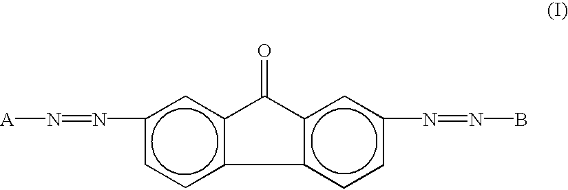
As a charge generation material which can be used for the photoreceptor of the present invention, a pigment which is sensitive to a long wavelength can be used. For example, phthalocyanine pigments such as metallic phthalocyanine and metal-free phthalocyanine, azulenium salt pigments, Squarilium salt pigments and azo pigments can be used. The relative mirror reflectance T1 can be preferably obtained by using a disazo pigment having the following formula (I). Particularly, a coupler residual group having the formula (II) can be preferably used in respect of sensitivity of the resultant photoreceptor.
The reason is still unapparent, however, a shape of the crystal particle and an agglomerating condition in forming a layer of the disazo pigment having the following formula (I) are considered to have some optical good effects. In addition, even if the disazo pigment is mixed with other heterogeneous pigments according to the wavelength to be absorbed, a sufficient effect can be expected.
Figure US06777149-20040817-C00001
wherein A and B independently represent a coupler residual
group having one of the following formulae (II) to (VIII).
Figure US06777149-20040817-C00002
wherein X1 represents —OH, —NHCOCH3 or —NHSO2CH3; Y1 represents —CON(R2)(R3), —CONHN═C(R6)(R7), —CONHN (R8)(R9), —CONHCONH(R12), a hydrogen atom, —COOH, —COOCH3, COOC6H5 or a benzimidazolyl group,
wherein R2 and R3 independently represent a hydrogen atom, a substituted or unsubstituted alkyl group, a substituted or unsubstituted aryl group and a substituted or unsubstituted hetero ring group; R2 and R3 optionally form a ring together with a nitrogen atom; R6 and R7 independently represent a hydrogen atom, a substituted or unsubstituted alkyl group, a substituted or unsubstituted aralkyl group, a substituted or unsubstituted aryl group, a substituted or unsubstituted styryl group and a substituted or unsubstituted hetero ring group; R6 and R7 optionally form a ring together with a carbon atom; R8 and R9 independently represent a hydrogen atom, a substituted or unsubstituted alkyl group, a substituted or unsubstituted aralkyl group, a substituted or unsubstituted aryl group, a substituted or unsubstituted styryl group and a substituted or unsubstituted hetero ring group; R8 and R9 optionally form a 5 or 6 membered ring, which optionally includes a condensed aromatic group; and R12 represents a substituted or unsubstituted alkyl group, a substituted or unsubstituted aryl group and a substituted or unsubstituted hetero ring group; and Z represents a residual group selected from the group consisting of groups which are combined with the adjacent benzene ring to form a naphthalene ring, an anthracene ring, a carbazole ring, a benzocarbazole ring, a dibenzocarbazole ring, a dibenzofuran ring, a benzonaphthofuran ring and a dibenzothiophene ring; or a residual ring needed to form a hetero ring, which optionally have a substituted group;
Figure US06777149-20040817-C00003
wherein R4 represents a hydrogen atom, a substituted or unsubstituted alkyl group, or a substituted or unsubstituted aryl group;
Figure US06777149-20040817-C00004
wherein R5 represents a hydrogen atom, a substituted or unsubstituted alkyl group, or a substituted or unsubstituted aryl group;
Figure US06777149-20040817-C00005
wherein Y represents a divalent aromatic hydrocarbon group or a divalent hetero ring including a nitrogen atom in the ring;
Figure US06777149-20040817-C00006
wherein Y represents a divalent aromatic hydrocarbon group or a divalent hetero ring including a nitrogen atom in the ring;
Figure US06777149-20040817-C00007
wherein R10 represents a hydrogen atom, a lower alkyl group having 1 to 6 carbon atoms, a carboxyl group or an ester of a carboxyl group; and Ar1 represents a substituted or unsubstituted aromatic hydrocarbon ring group; and
Figure US06777149-20040817-C00008
wherein R10 represents a hydrogen atom, a lower alkyl group having 1 to 6 carbon atoms, a carboxyl group or an ester of a carboxyl group; and Ar1 represents a substituted or unsubstituted aromatic hydrocarbon ring group.
Within the context of the present invention, the term “alkyl group” means a saturated hydrocarbyl group having from 1 to 16 carbons, preferably from 1 to 11 carbons. Preferred alkyl groups include, but are not limited to methyl, ethyl, propyl, butyl, pentyl, hexyl, heptyl, octyl, nonyl, decyl, and undecyl groups, either linear or branched. More preferred are methyl, ethyl, propyl, butyl, hexyl and undecyl.
Within the context of the present invention, the term “aryl group” means mono to hexavalent aromatic hydrocarbon groups made of aromatic hydrocarbon rings, preferably including but not limited to, phenyl, naphthyl, anthracenyl and pyrenyl, which may be unsubstited or substituted.
Within the context of the present invention, the term “aralkyl group” means a combination of one of the above mentioned aryl groups and one of the above mentioned alkyl groups, wherein the group is preferably attached to the molecule core through the alkyl portion of the group.
Within the context of the present invention, the term “hetero ring group” means mono-to-hexavalent aromatic heterocyclic groups having one or more aromatic heterocyclic rings. The aromatic heterocyclic rings include, but are not limited to, pyridinyl, quinolinyl, thiophenyl, furyl, oxazolyl, oxadiazolyl and carbazolyl, wherein the heterocyclic ring may be substituted or unsubtituted.
When any of the above noted aromatic (either aryl or heteroaryl) groups is substituted, the substituents can be selected from any substituent that does not interfere with the charge generation properties of the compound. Preferably the substituent includes, but is not limited to, one or more groups independently selected from alkyl having 1 to 16 carbons, alkoxy groups having 1 to 16 carbons, halogen groups and aryl groups as defined above. More preferably, the substituent(s) include one or more groups independently selected from methyl, ethyl, propyl, butyl, hexyl, undecyl, methoxy, ethoxy, propoxy, butoxy, fluoro, chloro, bromo, iodo and the above noted aryl groups.
Specific examples of the couplers forming a coupler residual group of the disazo pigments having the formula (I) are shown in Tables 1 to 16.
TABLE 1-1
Figure US06777149-20040817-C00009
Melting Point
Coupler No. R1 (R2)n (° C.)
1 H H 243 to 244
2 H 2-NO2 194 to 196
3 H 3-NO2 246 to 247
4 H 4-NO2   266 to 267.5
5 H 2-CF3 178 to 179
6 H 3-CF3 237.5 to 238.5
7 H 4-CF3 279 to 281
8 H 2-CN   221 to 222.5
9 H 3-CN 256.5 to 258.5
10 H 4-CN 274.5 to 277  
11 H 2-I   199 to 199.5
12 H 3-I 258.5 to 259.5
13 H 4-I 261.5 to 262  
14 H 2-Br 217 to 218
15 H 3-Br 254 to 255
16 H 4-Br 265 to 268
17 H 2-Cl 228 to 230
18 H 3-Cl 256.5 to 257  
TABLE 1-2
Melting Point
Coupler No. R1 (R2)n (° C.)
19 H 4-Cl 264 to 266
20 H 2-F 223.0 to 224.0
21 H 3-F 250.0 to 251.0
22 H 4-F 265.0 to 267.0
23 H 2-CH3 195.5 to 198.0
24 H 3-CH3 214.5 to 216.5
25 H 4-CH3 227.0 to 229.0
26 H 2-C2H5 168.5 to 169.5
27 H 4-C2H5 203.0 to 204.5
28 H 2-OCH3 167 to 168
29 H 3-OCH3 195.5 to 198.0
30 H 4-OCH3 229 to 230
31 H 2-OC2H5 157 to 158
32 H 3-OC2H5 188.5 to 189.0
33 H 4-OC2H5 225.0 to 225.5
34 H 4-N(CH3)2 232.0 to 233.5
35 —CH3 H 189.5 to 190.5
36
Figure US06777149-20040817-C00010
H 182.0 to 183.0
37 H 2-OCH3, 5-OCH3 186.0 to 188.0
38 H 2-OC2H5, 173.0 to 173.5
5-OC2H5
39 H 2-CH3, 5-CH3 207.0 to 208.5
40 H 2-Cl, 5-Cl 253.5 to 254.5
TABLE 1-3
Melting Point
Coupler No. R1 (R2)n (° C.)
41 H 2-CH3, 5-Cl 245 to 247
42 H 2-OCH3, 4-OCH3 151.0 to 152.0
43 H 2-CH3, 4-CH3 226 to 228
44 H 2-CH3, 4-Cl 244 to 245
45 H 2-NO2, 4-OCH3 179.5 to 181.0
46 H 3-OCH3, 5-OCH3 180.5 to 182.0
47 H 2-OCH3, 5-Cl 219.0 to 220.0
48 H 2-OCH3, 5-OCH3, 4-Cl 193.5 to 195.5
49 H 2-OCH3, 4-OCH3, 5-Cl 193 to 194
50 H 3-Cl, 4-Cl 272.5 to 273.5
51 H 2-Cl, 4-Cl, 5-Cl 257.5 to 258.5
52 H 2-CH3, 3-Cl 227.5 to 228.5
53 H 3-Cl, 4-CH3 259.5 to 260.5
54 H 2-F, 4-F 246.0 to 246.5
55 H 2-F, 5-F 259.0 to 260.0
56 H 2-Cl, 4-No2 283.0 to 284.0
57 H 2-No2, 4-Cl 226.5 to 227.5
58 H 2-Cl, 3-Cl, 4-Cl, 5-Cl 280.0 to 281.5
59 H 4-OH 268
TABLE 2-1
Figure US06777149-20040817-C00011
Melting Point
Coupler No. R1 (R2)n (° C.)
60 H H >300
61 H 2-NO2 283 to 284
62 H 3-NO2 >300
63 H 4-NO2 >300
64 H 2-Cl >300
65 H 3-Cl >300
66 H 4-Cl >300
67 H 2-CH3 >300
68 H 3-CH3 >300
69 H 4-CH3 >300
70 H 2-C2H5 271 to 273
71 H 4-C2H5 >300
72 H 2-OCH3 276 to 278
73 H 3-OCH3 >300
74 H 4-OCH3 >300
75 H 2-OC2H5 273.5 to 275.0
76 H 4-OC2H5 >300
77 H 2-CH3, 4-OCH3  296
TABLE 2-2
Melting Point
Coupler No. R1 (R2)n (° C.)
78 H 2-CH3, 4-CH3 >300
79 H 2-CH3, 5-CH3
80 H 2-CH3, 6-CH3
81 H 2-OCH3, 4-OCH3
82 H 2-OCH3, 5-OCH3
83 H 3-OCH3, 5-OCH3
84 H 2-CH3, 3-Cl
85 H 2-CH3, 4-Cl
86 H 2-CH3, 5-Cl
87 H
Figure US06777149-20040817-C00012
88 H 2-CH(CH3)2
TABLE 3-1
Figure US06777149-20040817-C00013
Melting Point
Coupler No. R1 (R2)n (° C.)
89 H H 228.0 to 230.0
90 H 4-N(CH3)2 238.5 to 240.0
91 H 2-OCH3 218.0 to 222.0
92 H 3-OCH3 186.5 to 188.5
93 H 4-OCH3 224.5 to 225.0
94 H 4-OC2H5 236.0 to 237.5
95 H 2-CH3 227.0 to 228.0
96 H 3-CH3 212.5 to 214.0
97 H 4-CH3 233.0 to 236.0
98 H 2-F 233.0 to 233.5
99 H 3-F 248.5
100 H 4-F 239.5 to 240.0
101 H 2-Cl 254.0 to 255.0
102 H 3-Cl 226.5 to 230.0
103 H 4-Cl 265.5 to 269.0
104 H 2-Br 243.0
105 H 3-Br 231.0 to 231.50
106 H 4-Br 259.0
TABLE 3-2
Melting
Coupler Point
No. R1 (R2)n (° C.)
107 H 2-Cl, 4-Cl 251.5 to
252.0
108 H 3-Cl, 4-Cl 260.0 to
261.0
109 H 2-CN 175.0 to
176.5
110 H 4-CN 267.5 to
268.0
111 H 2-NO2 240.0
112 H 3-NO2 255.5 to
257.0
113 H 4-NO2 260.0 to
261.0
114 H 2-CH3, 4-CH3 234.5 to
236.5
115 H 2-OCH3, 5-OCH3 221.5 to
222.0
116 H 2-OCH3, 3-OCH3 191.0 to
4-OCH3 192.0
117 —CH3 H 248.5 to
250.0
118
Figure US06777149-20040817-C00014
H 182.5 to 185.0
119
Figure US06777149-20040817-C00015
H 213.0 to 214.5
120 H
Figure US06777149-20040817-C00016
237.0 to 237.5
TABLE 4
Figure US06777149-20040817-C00017
Coupler Melting Point
No. R1 R2 (° C.)
121 —CH3 —CH3 232.5 to 233.0
122 H
Figure US06777149-20040817-C00018
208.5 to 209.0
123 H
Figure US06777149-20040817-C00019
224.0 to 224.5
124 H
Figure US06777149-20040817-C00020
197.5 to 199.0
125 H
Figure US06777149-20040817-C00021
188.0 to 188.5
126 H
Figure US06777149-20040817-C00022
227.0 to 228.0
127 —CH3
Figure US06777149-20040817-C00023
225.5 to 226.0
128 H
Figure US06777149-20040817-C00024
212.5 to 214.0
129 H
Figure US06777149-20040817-C00025
257
130 H
Figure US06777149-20040817-C00026
250
131 H
Figure US06777149-20040817-C00027
 32.5 to 236.0
132 H
Figure US06777149-20040817-C00028
240.5 to 241.5
TABLE 5
Figure US06777149-20040817-C00029
Coupler No. (R)n Melting Point (° C.)
133 H >300
134 2-OCH3  268
135 3-OCH3 281.0 to 283.0
136 4-OCH3  293
137 2-CH3  297
138 3-CH3  296
139 4-CH3 >300
140 4-Cl >300
141 2-NO2 >300
142 4-NO2 >300
143 2-OH >300
144 2-OH, 3-NO2 >300
145 2-OH, 5-NO2 >300
146 2-OH, 3-OCH3 >300
TABLE 6
Figure US06777149-20040817-C00030
Coupler No. (R)n Melting Point (° C.)
147 4-Cl >300
148 2-NO2  268
149 3-NO2 >300
150 4-NO2 >300
151
Figure US06777149-20040817-C00031
 296
152 H 300 to 307
153 2-OCH3 242 to 248
154 3-OCH3 269 to 275
155 4-OCH3  312
156 2-CH3 265 to 270
157 3-CH3 270 to 278
158 4-CH3  304
159 2-Cl 283 to 288
160 3-Cl 281 to 287
TABLE 7
Figure US06777149-20040817-C00032
Melting Point
Coupler No. R1 (R2)n (° C.)
161 H 2-OCH3, 4-Cl, 208.0 to 208.5
5-CH3
162 —OCH3 H 230.5 to 231.5
163 —OCH3 2-CH3 205.5 to 206.0
164 —OCH3 2-OCH3, 5-OCH3, 4-Cl 245.5 to 246.0
TABLE 8
Figure US06777149-20040817-C00033
Coupler No. X Melting Point (° C.)
165
Figure US06777149-20040817-C00034
207.0 to 209.0
166
Figure US06777149-20040817-C00035
257.0 to 259.0
167
Figure US06777149-20040817-C00036
290
TABLE 9
Figure US06777149-20040817-C00037
Coupler No. R1 Melting Point (° C.)
168
Figure US06777149-20040817-C00038
>300
169
Figure US06777149-20040817-C00039
>300
170
Figure US06777149-20040817-C00040
>300
171
Figure US06777149-20040817-C00041
298
TABLE 10
Figure US06777149-20040817-C00042
Coupler Melting Point
No. X R (° C.)
172
Figure US06777149-20040817-C00043
Figure US06777149-20040817-C00044
180 to 183
173
Figure US06777149-20040817-C00045
Figure US06777149-20040817-C00046
228.5 to 229.5
174
Figure US06777149-20040817-C00047
Figure US06777149-20040817-C00048
>262
175
Figure US06777149-20040817-C00049
Figure US06777149-20040817-C00050
226.5 to 227.0
176
Figure US06777149-20040817-C00051
Figure US06777149-20040817-C00052
308 to 310
177
Figure US06777149-20040817-C00053
Figure US06777149-20040817-C00054
222 to 223
TABLE 11
Figure US06777149-20040817-C00055
Melting
Coupler Point
No. R1 R2 (° C.)
178 H H 220.5 to
221.5
179 —CH3 H 190.5 to
192.5
180 —CH3 —CH3 196.0 to
198.0
181 H
Figure US06777149-20040817-C00056
222.0 to 223.0
TABLE 12-1
Coupler Melting Point
No. Structure (° C.)
182
Figure US06777149-20040817-C00057
>300
183
Figure US06777149-20040817-C00058
>300
184
Figure US06777149-20040817-C00059
>300
185
Figure US06777149-20040817-C00060
>300
186
Figure US06777149-20040817-C00061
>300
187
Figure US06777149-20040817-C00062
>300
188
Figure US06777149-20040817-C00063
122.0 to 122.5
TABLE 12-2
Coupler Melting Point
No. Structure (° C.)
189
Figure US06777149-20040817-C00064
222.5 to 224.0
190
Figure US06777149-20040817-C00065
74.5 to 75.5
191
Figure US06777149-20040817-C00066
275.5 to 276.5
192
Figure US06777149-20040817-C00067
130.5 to 131.5
193
Figure US06777149-20040817-C00068
>300
194
Figure US06777149-20040817-C00069
>300
195
Figure US06777149-20040817-C00070
>300
196
Figure US06777149-20040817-C00071
172.5 to 173.5
TABLE 12-3
Coupler Melting Point
No. Structure (° C.)
197
Figure US06777149-20040817-C00072
262.5 to 265.5
198
Figure US06777149-20040817-C00073
>300
199
Figure US06777149-20040817-C00074
>300
200
Figure US06777149-20040817-C00075
128.0 to 129.0
TABLE 13-1
Figure US06777149-20040817-C00076
Melting Point
Coupler No. R1 (R2)n (° C.)
201 Cl H >300
202 Cl 2-OCH3 >300
203 Cl 3-OCH3 >300
204 Cl 4-OCH3 >300
205 Cl 2-CH3 >300
206 Cl 3-CH3 >300
207 Cl 4-CH3 >300
208 Cl 2-Cl >300
209 Cl 3-Cl >300
210 Cl 4-Cl >300
211 Cl 2-NO2 >300
212 Cl 3-NO2 >300
213 Cl 4-NO2 >300
214 Cl 2-CH3, 4-Cl >300
215 Cl 2-CH3, 4-CH3 >300
216 Cl 2-C2H5 299.0 to
301.0
217 CH3 H >300
TABLE 13-2
Melting Point
Coupler No. R1 (R2)n (° C.)
218 CH3 2-OCH3   297
219 CH3 3-OCH3 >300
220 CH3 4-OCH3 >300
221 CH3 2-CH3 >300
222 CH3 3-OH3 >300
223 CH3 4-CH3 >300
224 CH3 2-Cl >300
225 CH3 3-Cl >300
226 CH3 4-Cl >300
227 CH3 2-NO2 >300
228 CH3 3-NO2 >300
229 CH3 4-NO2 >300
230 CH3 2-CH3, 4-Cl >300
231 CH3 2-CH3, 4-CH3 >300
232 CH3 2-C2H5 268.5 to 270.0
233 OCH3 H     289.0
234 OCH3 2-OCH3 268.0 to 270.0
235 OCH3 3-OCH3 >300
236 OCH3 4-OCH3 >300
237 OCH3 2-CH3 284.5 to 285.5
238 OCH3 3-CH3 >300
239 OCH3 4-CH3 >300
TABLE 13-3
Melting Point
Coupler No. R1 (R2)n (° C.)
240 OCH3 2-Cl >300
241 OCH3 3-Cl >300
242 OCH3 4-Cl >300
243 OCH3 2-NO2 >300
244 OCH3 3-NO2 >300
245 OCH3 4-NO2 >300
246 OCH3 2-C2H5 264.5 to
266.5
TABLE 14-1
Coupler No. Structure
247
Figure US06777149-20040817-C00077
248
Figure US06777149-20040817-C00078
249
Figure US06777149-20040817-C00079
250
Figure US06777149-20040817-C00080
251
Figure US06777149-20040817-C00081
252
Figure US06777149-20040817-C00082
253
Figure US06777149-20040817-C00083
TABLE 14-2
Coupler No. Structure
254
Figure US06777149-20040817-C00084
255
Figure US06777149-20040817-C00085
256
Figure US06777149-20040817-C00086
257
Figure US06777149-20040817-C00087
258
Figure US06777149-20040817-C00088
TABLE 15
Figure US06777149-20040817-C00089
Coupler No. (R2)n
259 2-Cl, 3-Cl
260 2-Cl, 4-Cl
261 3-Cl, 5-Cl
TABLE 16
Figure US06777149-20040817-C00090
Coupler No. (R2)n
262 4-CH3
263 3-NO2
264 2-Cl
265 3-Cl
266 4-Cl
267 2-Cl, 3-Cl
268 2-Cl, 4-Cl
269 3-Cl, 5-Cl
270 2-Cl, 5-Cl
271 3-Cl, 4-Cl
The charge generation layer can be formed by the following method:
(1) the above-mentioned charge generation materials are dispersed in a liquid solution of a binder resin such as polyester resins, polycarbonate resins, polyvinylbutyral resins and acrylic resins by a ball mill, an attritor, a sand mill, etc; and
(2) the dispersed liquid is properly diluted and coated on a substrate by a dip coating, a spray coating, a bead coating method, etc.
The relative mirror reflectance T1 of the present invention changes in accordance with the charge generation material. However, T1 can be also controlled by the dispersed condition of the charge generation material, and the affinity and mixing ratio of the pigment and the binder resin as well as the composition of the above-mentioned intermediate layer.
The charge generation layer preferably has a thickness of from 0.01 to 5 μm, and more preferably from 0.1 to 2 μm.
Charge Transport Layer
The charge transport layer is formed from a charge transport material and a binder resin which is optionally used.
The material is dissolved or dispersed in a proper solvent, and the liquid solution is coated on a substrate and dried to form the charge transport layer.
As the charge transport materials, there are a hole transport material and an electron transport material.
Specific examples of the hole transport materials include electron imparting materials such as poly-N-vinylcarbazole and its derivatives, poly-γ-carbazolylethylgultamate and its derivatives, pyrene-formaldehyde condensates and their derivatives, polyvinylpyrene, polyvinylphenanthrene, oxazole derivatives, oxadiazole derivatives, imidazole derivatives, triphenylamine derivatives, 9-(P-diethylaminostyryl)anthracene, 1,1-bis-(4-dibenzylaminophenyl)propane, styrylanthracene, styrylpyrazoline, phenylhydrazone compounds and α-phenylstilbene derivatives.
Specific examples of the electron transport materials include electron accepting materials such as chloranil, bromoanil, tetracyanoethylene, tetracyanoquinodimethane, 2,4,7-trinitro-9-fluorenone, 2,4,5,7-tetranitro-9-fluorenone, 2,4,5,7-tetranitroxanthone, 2,4,8-trinitrothioxanthone, 2,6,8-trinitro-indeno [1,2-b] thiophene-4-one and 1,3,7-trinitrodibenzothiophene-5,5-dioxide. These charge transport materials can be used alone or in combination.
Specific examples of the binder resins for optional use in the present invention include thermoplastic or thermosetting resins such as polystyrene resins, styrene-acrylonitrile copolymers, styrene-butadiene copolymers, styrene-maleic anhydride copolymers, polyester resins, polyvinyl chloride resins, vinyl chloride-vinyl acetate copolymers, polyvinyl acetate resins, polyvinylidene chloride resins, polyarylate resins, polycarbonate resins, cellulose acetate resins, ethyl cellulose resins, polyvinyl butyral resins, polyvinyl formal resins, polyvinyl toluene resins, poly-N-vinylcarbazole resins, acrylic resins, silicone resins, epoxy resins, melamine resins, urethane resins, phenol resins and alkyd resins.
Specific examples of the solvents include tetrahydrofuran, dioxane, toluene, monochlorobenzene, dichloroethane, methylene chloride, etc.
The charge transport layer preferably has a thickness of from 5 to 100 μ/m.
In addition, a plasticizer and a leveling agent can be included in the charge transport layer of the present invention. As the plasticizer, conventional plasticizers for resins, such as dibutylphthalate and dioctylphthalate can be used. The content of the plasticizer is preferably from 0 to 30% by weight per 100% by weight of the binder resin. As the leveling agent, silicone oils such as dimethyl silicone oils and methyl phenyl silicone oils can be used. The content of the leveling agent is preferably from 0 to 1% by weight per 100% by weight of the binder resin.
In addition, an insulating layer and a protective layer can be formed on the photosensitive layer in the present invention.
Electroconductive Substrate
The substrate used for the photoreceptor of the present invention is formed as follows. Metals such as aluminium and nickel are deposited or laminated on metallic drums and sheets such as aluminium, brass, stainless and nickel; polyethyleneterephthalate; polypropylene; nylon; paper, etc. Among the substrates, a cylindrical drum formed of aluminium or its alloyed metals is widely used at present. Particularly, non-cut aluminium tube without a cutting process is preferably used because the manufacturing cost is lower and the adherence to the photosensitive layer is higher than that of a conventional cut aluminium tube.
In addition, the photoreceptor having the relative mirror reflectance of the present invention can prevent image-density irregularity of the resultant image even if the non-cut aluminium tube is used for the substrate.
Such aluminium alloys are formed by the method disclosed in JIS3003, 5000, 6000, etc. and the non-cut aluminium tube is formed by a conventional method such as EI, ED, DI and II methods.
In addition, neither a surface cut process and grind with a diamond turning tool, etc. nor a surface treatment such as anodizing is performed on the aluminium tube.
Electrophotographic Device and Method
Next, the electrophotographic process and device of the present invention will be explained in detail, referring to the drawings.
FIG. 4 is a schematic view for explaining the electrophotographic process and device of the present invention, and the following modified example also belongs to the present invention. In FIG. 4, a photoreceptor 1 includes a drum substrate on which a photosensitive layer is formed. For a charger 3, a pre-transfer charger 7, a transfer charger 10, a separation charger 11 and a pre-cleaning charger 13, known chargers such as corotrons, scorotrons, solid state chargers and charging rollers are used. For the transfer means, the above-mentioned chargers can be used, however, a combination of a transfer charger 10 and a separation charger 11 as shown in FIG. 4 is effectively used. For an image irradiator 5, coherent light such as light emitting diodes (LEDS), laser diode (LDs) and electroluminescence (EL) lamps is used. As a light source for a discharging lamp 2, etc., any known illuminators such as fluorescent lamps, tungsten lamps, halogen lamps, mercury lamps, sodium lamps, light emitting diodes (LEDs), laser diodes (LDs) and electro luminescense (EL) lamps can be used. In order to irradiate only the light having a desired wavelength, various filters such as sharp cut filters, band pass filters, near infrared cutting filters, dichroic filters, interference filters and conversion filters can be also used. Such light sources can be also used for irradiating the photoreceptor in processes such as a transfer process combined with light irradiation, a charge eliminating process, a cleaning process, a pre-exposure process, etc. as well as the processes mentioned above.
Toner images formed on the photoreceptor 1 by developing unit 6 are transferred on a transfer paper 9. However, all of the toner particles of the toner images are not transferred on the transfer paper 9 and there also remain toner particles on the photoreceptor 1. Such toner particles are removed from photoreceptors by a fur brush 14 and a blade 15. Cleaning may be made only by a known cleaning brush such as fur brushes and mag-fur brushes.
When a photoreceptor is charge positively (negatively) and image exposure is performed, positive (negative) electrostatic latent images are formed on the surface of the photoreceptor. Positive images are obtained when the latent images are developed with negatively-charged (positively-charged) toners and negative images are obtained when the latent images are developed with positively-charged (negatively-charged) toners. As the developing method, known developing methods can be applied. In addition, known discharging methods can be used for discharging the charges remaining on the photoreceptor.
FIG. 5 shows another embodiment of the electrophotographic process of the present invention. A photoreceptor 21 has the photosensitive layer of the present invention, and is driven by driving rollers 22 a and 22 b. The photoreceptor 21 is charged by a charger 23, and exposed to light emitted by a light source 24 to form a latent image thereon. Then the latent image is developed by an image developer (not illustrated) to form a toner image thereon. The toner image is transferred on a transfer paper (not shown) using a charger 25. The photoreceptor 21 is then subjected to a cleaning pre-exposure treatment using a light source 26, a cleaning treatment using a brush 27 and a discharging treatment using a light source 28. These processes are repeatedly performed to produce images. In FIG. 5, pre-cleaning light irradiates the photoreceptor 21 from the substrate side. (In this case, the substrate is transparent.)
For instance, in FIG. 5, although the cleaning pre-exposure is made from the substrate side, the cleaning pre-exposure may be made from the photosensitive layer side. In addition, irradiation of image exposure and discharging can be made from the substrate side. With respect to the light irradiation processes, the image exposure, cleaning pre-exposure and discharging exposure are illustrated. However, light irradiation such as pre-transfer exposure, pre-exposure of image exposure and other known light irradiation processes can be made to the photoreceptors.
The electrophotographic device as mentioned above can be fixedly installed into copiers, facsimiles and printers. In addition, they can be installed into these devices in the form of a process cartridge as well. The process cartridge is a device (part) containing at least a photoreceptor, and at least one of a charger, an image irradiator, an image developer, an image transfer, a cleaner and a discharger. There are many types of process cartridges, however, FIG. 6 is a schematic view illustrating an embodiment of the process cartridge of the present invention. A photoreceptor 16 has a photosensitive layer of the present invention.
Having generally described this invention, further understanding can be obtained by reference to certain specific examples which are provided herein for the purpose of illustration only and are not intended to be limiting. In the descriptions in the following examples, the numbers represent weight ratios in parts, unless otherwise specified.
EXAMPLES Example 1
After 100 parts of a polyamide resin (FR101 from Namariichi Co., Ltd.) and 100 parts of a melamine resin (Super Bekkamin G-821-50 from Dainippon Ink & Chemicals, Inc.) were dissolved in 850 parts of methanol, 600 parts of a fine powder of titanium oxide (TP-2 from Fuji Titanium Industry Co., Ltd.) were added into the solution and the solution was stirred for 120 hrs by a ball mill. Then, 350 parts of methanol was further added into the solution to dilute the solution and prepare a coating liquid for an intermediate layer. The liquid was coated on an aluminium-deposited polyester film (Lumirror from Toray Industries, Inc.), and dried for 20 min at 150° C. to form an intermediate layer having a thickness of 5 μm. The relative mirror reflectance of the thus formed intermediate layer against an aluminium-deposited mirror at an incident angle of 5° was measured by a self-recording spectrophotometer (UV-3100 from Shimadzu Corp.). The results were as follows:
3.5% at a wavelength of 780 nm; and
3.1% at a wavelength of 650 nm.
Example 2
After 100 parts of a polyamide resin (FR101 from Namariichi Co., Ltd.) and 100 parts of a melamine resin (Super Bekkamin G-821-50 from Dainippon Ink & Chemicals, Inc.) were dissolved in 1000 parts of methanol, 900 parts of a fine powder of titanium oxide (TP-2 from Fuji Titanium Industry Co., Ltd.) were added into the solution and the solution was stirred for 72 hrs by a ball mill. Then, 700 parts of methanol was further added into the solution to dilute the solution and prepare a coating liquid for an intermediate layer. The liquid was coated on an aluminium-deposited polyester film (Lumirror from Toray Industries, Inc.), and dried for 20 min at 150° C. to form an intermediate layer having a thickness of 5 am. The relative mirror reflectance of the thus formed intermediate layer against an aluminium-deposited mirror at an incident angle of 5° was measured by a self-recording spectrophotometer (UV-3100 from Shimadzu Corp.). The results were as follows:
4.1% at a wavelength of 780 nm; and
3.7% at a wavelength of 650 nm.
Examples 3 and 4
On the intermediate layers formed in Examples 1 and 2, a coating liquid for a charge generation layer having the following components which were mixed and stirred by a ball mill for 120 hrs, was coated and dried to form a charge generation layer having a thickness of 0.5 μm.
A disazo pigment 5 having the following formula (A)
Figure US06777149-20040817-C00091
A polyvinylbutyral resin 1
(S-LEC BM-S from Sekisui Chemical Co., Ltd.)
Cyclohexanone 250
The relative mirror reflectance of the thus formed intermediate layers and charge generation layers against an aluminium-deposited mirror at an incident angle of 5° was measured by a self-recording spectrophotometer (UV-3100 from Shimadzu Corp.). The results were as follows:
2.8% and 3.1% respectively at a wavelength of 780 nm; and
2.6% and 2.9% respectively at a wavelength of 650 nm.
Examples 5 and 6
On the intermediate layers formed in Examples 1 and 2, a coating liquid for a charge generation layer having the following components which were mixed and stirred by a ball mill for 120 hrs, was coated and dried to form a charge generation layer having a thickness of 0.5 μm.
A disazo pigment 1.5 having the following formula (A)
Figure US06777149-20040817-C00092
A polyvinylbutyral resin 1
(XYHL from Union Carbide Corp.)
Cyclohexanone 250
The relative mirror reflectance of the thus formed intermediate layers and charge generation layers against an aluminium-deposited mirror at an incident angle of 50 was measured by a self-recording spectrophotometer (UV-3100 from Shimadzu Corp.). The results were as follows:
2.6% and 2.9% respectively at a wavelength of 780 nm; and
2.4% and 2.7% respectively at a wavelength of 650 nm.
Comparative Examples 1 and 2
On the intermediate layers formed in Examples 1 and 2, a coating liquid for a charge generation layer having the following components which were mixed and stirred by a ball mill for 24 hrs, was coated and dried to form a charge generation layer having a thickness of 0.3 μm.
A-type titanylphthalocyanine 5
A polyvinylbutyral resin 5
(S-LEC BM-S from Sekisui Chemical Co., LTD.)
Methyl ethyl ketone 350
The relative mirror reflectance of the thus formed intermediate layers and charge generation layers against an aluminium-deposited mirror at an incident angle of 5° was measured by a self-recording spectrophotometer (UV-3100 from Shimadzu Corp.). The results were as follows:
4.0% and 4.5% respectively at a wavelength of 780 nm; and
3.6% and 4.1% respectively at a wavelength of 650 nm.
Examples 7 and 8
On the intermediate layers formed in Examples 1 and 2, a coating liquid for a charge generation layer having the following components which were mixed and stirred by a ball mill for 120 hrs, was coated and dried to form a charge generation layer having a thickness of 0.4 μm.
A-type titanylphthalocyanine 5
A disazo pigment 5
having the following formula (B)
Figure US06777149-20040817-C00093
A polyvinylbutyral resin 5
(S-LEC BM-S from Sekisui Chemical Co., LTD.)
Cyclohexanone 250
The relative mirror reflectance of the thus formed intermediate layers and charge generation layers against an aluminium-deposited mirror at an incident angle of 5° was measured by a self-recording spectrophotometer (UV-3100 from Shimadzu Corp.). The results were as follows:
2.9% and 3.3 respectively at a wavelength of 780 nm; and
2.7% and 3.1% respectively at a wavelength of 650 nm.
Examples 9 to 14 and Comparative Examples 3 to 4
The procedures of Examples 3 to 8 and Comparative Examples 1 to 2 were repeated except that each coating liquid was coated on a non-cut aluminium tube formed by an ED method, having an outer diameter of 30 mm and a length of 340 mm. A coating liquid for a charge transport layer having the following components was further coated on each coated tube, and dried to form a charge transport layer having a thickness of 20 μm.
4-diethylaminobenzaldehyde-1-benzyl-1-phenylhydrazne 7
Polycarbonate 10
(Iupilon from Mitsubishi Gas Chemical Co., Inc.)
Tetrahydrofuran 76
Thus, photoreceptors of Examples 9 to 14 and Comparative Examples 3 to 4 were prepared.
Examples 15 to 20 and Comparative Examples 5 to 6
The procedures for preparation of photoreceptors of Examples 9 to 14 and Comparative Examples 3 to 4 were repeated except for using a cut aluminium having an outer diameter of 30 mm and a length of 340 mm.
After the thus prepared photoreceptors of Examples 9 to 20 and Comparative Examples 3 to 6 were installed in the electrophotographic process cartridge shown in FIG. 6, each process cartridge was installed in the following electrophotographic processes A to E shown in FIG. 4.
Wavelength of
light source for Diameter of image
image irradiator writing light beam Light spot interval/
(LD) by a polygon mirror overlapped area
A 780 nm 75 × 85 μm 64 μm/44%
B 780 nm 50 × 60 μm 42 μm/50%
C 780 nm 55 × 70 μm 55 μm/70%
D 650 nm 30 × 40 μm 21 μm/95%
E 650 nm 16 × 20 μm 11 μm/98%
A halftone image was produced from each electrophotographic process and the image-density irregularity due to light interference was evaluated. The results are shown in Table 17.
TABLE 17
RMR- RMR- Sub- IDI
IL CG strate A B C D E
Ex. 9 3.5/3.1 2.8/2.6 Non-cut
Ex. 10 4.1/3.7 3.1/2.9 Non-cut Δ
Ex. 11 3.5/3.1 2.6/2.4 Non-cut
Ex. 12 4.1/3.7 2.9/2.7 Non-cut Δ
Com. Ex. 3.5/3.1 4.0/3.6 Non-cut Δ Δ X Δ X
3
Com. Ex. 4.1/3.7 4.5/4.1 Non-cut X X X X X
4
Ex. 13 3.5/3.1 2.9/2.7 Non-cut
Ex. 14 4.1/3.7 3.3/3.1 Non-cut Δ Δ Δ X
Ex. 15 3.5/3.1 2.8/2.6 Cut
Ex. 16 4.1/3.7 3.1/2.9 Cut
Ex. 17 3.5/3.1 2.6/2.4 Cut
Ex. 18 4.1/3.7 2.9/2.7 Cut
Com. Ex. 3.5/3.1 4.0/3.6 Cut Δ Δ Δ Δ X
5
Com. Ex. 4.1/3.7 4.5/4.1 Cut X X X X X
6
Ex. 19 3.5/3.1 2.9/2.7 Cut
Ex. 20 4.1/3.7 3.3/3.1 Cut Δ
RMR-IL: Relative mirror reflectance of intermediate layer
RMR-CGL: Relative mirror reflectance of charge generation layer
IDI: Image-density irregularity
◯: Image-density irregularity did not occur
Δ: Image-density irregularity slightly occurred
X: Image-density irregularity occurred
On the other hand, durability test for Example 9 and Comparative Example 15 was performed by producing continuous 50,000 images. It was observed that the end of the photosensitive layer of the photoreceptor of Example 15 was partly peeled off, and that the non-cut aluminium tube used in Example 9 had higher adherence to the photosensitive layer than that of Example 15.
This document claims priority and contains subject matter related to Japanese Patent Application No. 2001-086067 filed on Mar. 23, 2001, incorporated herein by reference.
Having now fully described the invention, it will be apparent to one of ordinary skill in the art that many changes and modifications can be made thereto without departing from the spirit and scope of the invention as set forth therein.

Claims (21)

What is claimed as new and desired to be secured by Letters Patent of the United States is:
1. An image forming apparatus comprising:
an image irradiator configured to irradiate a photoreceptor with a coherent light beam while scanning to form pixel light spots thereon for forming an electrostatic latent image thereon, wherein the light spots overlap with adjacent light spots; and
an image developer configured to develop the electrostatic latent image with a developer,
wherein the photoreceptor comprises an intermediate layer located overlying an electroconductive substrate, a charge generation layer located overlying the intermediate layer and a charge transport layer located overlying the charge generation layer, wherein the charge generation layer satisfies the following relationship:
T1≦3.5%
wherein T1 represents a relative mirror reflectance of the charge generation layer against the coherent light beam when the coherent light beam irradiates the charge generation layer at an incident angle of 5°.
2. The image forming apparatus of claim 1, wherein the intermediate layer and the charge generation layer satisfy the following relationship:
T1≦T2≦3.5%
wherein T2 represents a relative mirror reflectance of the intermediate layer against the coherent light when the coherent light irradiates the intermediate layer at an incident angle of 5°.
3. The image forming apparatus of claim 1, wherein each of the pixel light spots has a diameter not greater than 40 μm and the overlapped area is not less than 50% of the area of each of the light spots.
4. The image forming apparatus of claim 1, wherein the electroconductive substrate comprises a non-cut aluminum substrate.
5. The image forming apparatus of claim 4, wherein said non-cut aluminum substrate is formed by a drawing method.
6. The image forming apparatus of claim 1, wherein the charge generation layer comprises a disazo pigment having the following formula (I):
Figure US06777149-20040817-C00094
wherein A and B independently represent a coupler residual group having one of the following formulae (II) to (VIII)
Figure US06777149-20040817-C00095
wherein X1 represents —OH, —NHCOCH3 or —NHSO2CH3; Y1 represents —CON(R2)(R3), —CONHN═C (R6)(R7), —CONHN (R8)(R9), —CONHCONH(R12), a hydrogen atom, —COOH, —COOCH3, COOC6H5 or a benzimidazolyl group,
wherein R2 and R3 independently represent a hydrogen atom, a substituted or unsubstituted alkyl group, a substituted or unsubstituted aryl group and a substituted or unsubstituted hetero ring group; R2 and R3 optionally form a ring together with a nitrogen atom; R6 and R7 independently represent a hydrogen atom, a substituted or unsubstituted alkyl group, a substituted or unsubstituted aralkyl group, a substituted or unsubstituted aryl group, a substituted or unsubstituted styryl group and a substituted or unsubstituted hetero ring group; R6 and R7 optionally form a ring together with a carbon atom; R8 and R9 independently represent a hydrogen atom, a substituted or unsubstituted alkyl group, a substituted or unsubstituted aralkyl group, a substituted or unsubstituted aryl group, a substituted or unsubstituted styryl group and a substituted or unsubstituted hetero ring group; R8 and R9 optionally form a 5 or 6 membered ring, which optionally includes a condensed aromatic group; and R12 represents a substituted or unsubstituted alkyl group, a substituted or unsubstituted aryl group and a substituted or unsubstituted hetero ring group; and Z represents a residual group selected from the group consisting of groups which are combined with the adjacent benzene ring to form a naphthalene ring, an anthracene ring, a carbazole ring, a benzocarbazole ring, a dibenzocarbazole ring, a dibenzofuran ring, a benzonaphthofuran ring and a dibenzothiophene ring; or a residual ring needed to form a hetero ring, which optionally have a substituted group;
Figure US06777149-20040817-C00096
wherein R4 represents a hydrogen atom, a substituted or unsubstituted alkyl group, or a substituted or unsubstituted aryl group;
Figure US06777149-20040817-C00097
wherein R5 represents a hydrogen atom, a substituted or unsubstituted alkyl group, or a substituted or unsubstituted aryl group;
Figure US06777149-20040817-C00098
wherein Y represents a divalent aromatic hydrocarbon group or a divalent hetero ring including a nitrogen atom in the ring;
Figure US06777149-20040817-C00099
wherein Y represents a divalent aromatic hydrocarbon group or a divalent hetero ring including a nitrogen atom in the ring;
Figure US06777149-20040817-C00100
wherein R10 represents a hydrogen atom, a lower alkyl group having 1 to 6 carbon atoms, a carboxyl group or an ester of a carboxyl group; and Ar1 represents a substituted or unsubstituted aromatic hydrocarbon ring group; and
Figure US06777149-20040817-C00101
wherein R10 represents a hydrogen atom, a lower alkyl group having 1 to 6 carbon atoms, a carboxyl group or an ester of a carboxyl group; and Ar1 represents a substituted or unsubstituted aromatic hydrocarbon ring group.
7. An electrophotographic photoreceptor comprising an intermediate layer located overlying an electroconductive substrate, a charge generation layer located overlying the intermediate layer and a charge transport layer located overlying the charge generation layer, wherein the charge generation layer satisfies the following relationship:
T1≦3.5%
wherein T1 represents a relative mirror reflectance of the charge generation layer against a coherent light beam when the coherent light beam irradiates the charge generation layer at an incident angle of 5°.
8. The electrophotographic photoreceptor of claim 7, wherein the intermediate layer and the charge generation layer satisfy the following relationship:
T1≦T2≦3.5%
wherein T2 represents a relative mirror reflectance of the intermediate layer against the coherent light beam when the coherent light beam irradiates the intermediate layer at an incident angle of 5°.
9. The electrophotographic photoreceptor of claim 7, wherein the electroconductive substrate comprises a non-cut aluminum substrate.
10. The electrophotographic photoreceptor of claim 9, wherein said non-cut aluminum substrate is formed by a drawing process.
11. The electrophotographic photoreceptor of claim 7, wherein the charge generation layer comprises a disazo pigment having the following formula (I)
Figure US06777149-20040817-C00102
wherein A and B independently represent a coupler residual group having one of the following formulae (II) to (VIII);
Figure US06777149-20040817-C00103
wherein X1 represents —OH, —NHCOCH3 or —NHSO2CH3; Y1 represents —CON(R2)(R3), —CONHN═C(R6)(R7), —CONHN(R8)(R9), —CONHCONH(R12) a hydrogen atom, —COOH, —COOCH3, COOC6H5 or a benzimidazolyl group,
wherein R2 and R3 independently represent a hydrogen atom, a substituted or unsubstituted alkyl group, a substituted or unsubstituted aryl group and a substituted or unsubstituted hetero ring group; R2 and R3 optionally form a ring together with a nitrogen atom; R6 and R7 independently represent a hydrogen atom, a substituted or unsubstituted alkyl group, a substituted or unsubstituted aralkyl group, a substituted or unsubstituted aryl group, a substituted or unsubstituted styryl group and a substituted or unsubstituted hetero ring group; R6 and R7 optionally form a ring together with a carbon atom; R8 and R9 independently represent a hydrogen atom, a substituted or unsubstituted alkyl group, a substituted or unsubstituted aralkyl group, a substituted or unsubstituted aryl group, a substituted or unsubstituted styryl group and a substituted or unsubstituted hetero ring group; R8 and R9 optionally form a 5 or 6 membered ring, which optionally includes a condensed aromatic group; and R12 represents a substituted or unsubstituted alkyl group, a substituted or unsubstituted aryl group and a substituted or unsubstituted hetero ring group; and Z represents a residual group selected from the group consisting of groups which are combined with the adjacent benzene ring to form a naphthalene ring, an anthracene ring, a carbazole ring, a benzocarbazole ring, a dibenzocarbazole ring, a dibenzofuran ring, a benzonaphthofuran ring and a dibenzothiophene ring; or a residual ring needed to form a hetero ring, which optionally have a substituted group;
Figure US06777149-20040817-C00104
wherein R4 represents a hydrogen atom, a substituted or unsubstituted alkyl group, or a substituted or unsubstituted aryl group;
Figure US06777149-20040817-C00105
wherein R5 represents a hydrogen atom, a substituted or unsubstituted alkyl group, or a substituted or unsubstituted aryl group;
Figure US06777149-20040817-C00106
wherein Y represents a divalent aromatic hydrocarbon group or a divalent hetero ring including a nitrogen atom in the ring;
Figure US06777149-20040817-C00107
wherein Y represents a divalent aromatic hydrocarbon group or a divalent hetero ring including a nitrogen atom in the ring;
Figure US06777149-20040817-C00108
wherein R10 represents a hydrogen atom, a lower alkyl group having 1 to 6 carbon atoms, a carboxyl group or an ester of a carboxyl group; and Ar1 represents a substituted or unsubstituted aromatic hydrocarbon ring group; and
Figure US06777149-20040817-C00109
wherein R10 represents a hydrogen atom, a lower alkyl group having 1 to 6 carbon atoms, a carboxyl group or an ester of a carboxyl group; and Ar1 represents a substituted or unsubstituted aromatic hydrocarbon ring group.
12. A process cartridge comprising:
a photoreceptor, and
at least one member selected from the group consisting of:
a charger configured to charge the photoreceptor;
an image irradiator configured to irradiate the photoreceptor to form an electrostatic latent image thereon;
an image developer configured to develop the electrostatic latent image with a developer to form a toner image on the photoreceptor;
an image transferer configured to transfer the toner image onto a receiving material;
a cleaner configured to remove residual toner on the photoreceptor; and
a discharger configured to discharge a residual potential of the photoreceptor,
wherein the photoreceptor comprises an intermediate layer located overlying an electroconductive substrate, a charge generation layer located overlying the intermediate layer and a charge transport layer located overlying the charge generation layer, wherein the charge generation layer satisfies the following relationship:
T1≦3.5%
wherein T1 represents a relative mirror reflectance of the charge generation layer against a coherent light beam when the coherent light beam irradiates the charge generation layer at an incident angle of 5°.
13. The process cartridge of claim 12, wherein the intermediate layer and the charge generation layer satisfy the following relationship:
T1≦T2≦3.5%
wherein T2 represents a relative mirror reflectance of the intermediate layer against the coherent light beam when the coherent light beam irradiates the intermediate layer at an incident angle of 5°.
14. The process cartridge of claim 12, wherein the electroconductive substrate comprises a non-cut aluminum substrate.
15. The process cartridge of claim 14, wherein the non-cut aluminum substrate is formed by a drawing process.
16. The process cartridge of claim 12, wherein the charge generation layer comprises a disazo pigment having the following formula (I):
Figure US06777149-20040817-C00110
wherein A and B independently represent a coupler residual group having one of the following formulae (II) to (VIII);
Figure US06777149-20040817-C00111
wherein X1 represents —OH, —NHCOCH3 or —NHSO2CH3; Y1 represents —CON(R2)(R3), —CONHN═C(R6)(R7), —CONHN(R8)(R9), —CONHCONH(R12), a hydrogen atom, —COOH, —COOCH3, COOC6H5 or a benzimidazolyl group,
wherein R2 and R3 independently represent a hydrogen atom, a substituted or unsubstituted alkyl group, a substituted or unsubstituted aryl group and a substituted or unsubstituted hetero ring group; R2 and R3 optionally form a ring together with a nitrogen atom; R6 and R7 independently represent a hydrogen atom, a substituted or unsubstituted alkyl group, a substituted or unsubstituted aralkyl group, a substituted or unsubstituted aryl group, a substituted or unsubstituted styryl group and a substituted or unsubstituted hetero ring group; R6 and R7 optionally form a ring together with a carbon atom; R8 and R9 independently represent a hydrogen atom, a substituted or unsubstituted alkyl group, a substituted or unsubstituted aralkyl group, a substituted or unsubstituted aryl group, a substituted or unsubstituted styryl group and a substituted or unsubstituted hetero ring group; R8 and R9 optionally form a 5 or 6 membered ring, which optionally includes a condensed aromatic group; and R12 represents a substituted or unsubstituted alkyl group, a substituted or unsubstituted aryl group and a substituted or unsubstituted hetero ring group; and Z represents a residual group selected from the group consisting of groups which are combined with the adjacent benzene ring to form a naphthalene ring, an anthracene ring, a carbazole ring, a benzocarbazole ring, a dibenzocarbazole ring, a dibenzofuran ring, a benzonaphthofuran ring and a dibenzothiophene ring; or a residual ring needed to form a hetero ring, which optionally have a substituted group;
Figure US06777149-20040817-C00112
wherein R4 represents a hydrogen atom, a substituted or unsubstituted alkyl group, or a substituted or unsubstituted aryl group;
Figure US06777149-20040817-C00113
wherein R5 represents a hydrogen atom, a substituted or unsubstituted alkyl group, or a substituted or unsubstituted aryl group;
Figure US06777149-20040817-C00114
wherein Y represents a divalent aromatic hydrocarbon group or a divalent hetero ring including a nitrogen atom in the ring;
Figure US06777149-20040817-C00115
wherein Y represents a divalent aromatic hydrocarbon group or a divalent hetero ring including a nitrogen atom in the ring;
Figure US06777149-20040817-C00116
wherein R10 represents a hydrogen atom, a lower alkyl group having 1 to 6 carbon atoms, a carboxyl group or an ester of a carboxyl group; and Ar1 represents a substituted or unsubstituted aromatic hydrocarbon ring group; and
Figure US06777149-20040817-C00117
wherein R10 represents a hydrogen atom, a lower alkyl group having 1 to 6 carbon atoms, a carboxyl group or an ester of a carboxyl group; and Ar1 represents a substituted or unsubstituted aromatic hydrocarbon ring group.
17. An electrophotographic image forming method comprising;
irradiating a photoreceptor with coherent light to form an electrostatic latent image thereon; and
developing the electrostatic latent image with a developer,
wherein the photoreceptor comprises an intermediate layer located overlying an electroconductive substrate, a charge generation layer located overlying the intermediate layer and a charge transport layer located overlying the charge generation layer, wherein the charge generation layer satisfies the following relationship:
T1≦3.5%
wherein T1 represents a relative mirror reflectance of the charge generation layer against the coherent light beam when the coherent light beam irradiates the charge generation layer at an incident angle of 5°.
18. The electrophotographic image forming method of claim 17, wherein the intermediate layer and the charge generation layer satisfy the following relationship:
T1≦T2≦3.5%
wherein T2 represents a relative mirror reflectance of the intermediate layer against the coherent light beam when the coherent light beam irradiates the intermediate layer at an incident angle of 5°.
19. The electrophotographic image forming method of claim 17, wherein the electroconductive substrate comprises a non-cut aluminum substrate.
20. The electrophotographic image forming method of claim 19, wherein the non-cut aluminum substrate is formed by a drawing process.
21. The electrophotographic image forming method of claim 17, wherein the charge generation layer comprises a disazo pigment having the following formula (I)
Figure US06777149-20040817-C00118
wherein A and B independently represent a coupler residual group having one of the following formulae (II) to (VIII);
Figure US06777149-20040817-C00119
wherein X1 represents —OH, —NHCOCH3 or —NHSO2CH3; Y1 represents —CON(R2)(R 3), —CONHN═C(R6)(R7), —CONHN(R8)(R9), —CONHCONH(R12), a hydrogen atom, —COOH, —COOCH3, COC6H5 or a benzimidazolyl group,
wherein R2 and R3 independently represent a hydrogen atom, a substituted or unsubstituted alkyl group, a substituted or unsubstituted aryl group and a substituted or unsubstituted hetero ring group; R2 and R3 optionally form a ring together with a nitrogen atom; R6 and R7 independently represent a hydrogen atom, a substituted or unsubstituted alkyl group, a substituted or unsubstituted aralkyl group, a substituted or unsubstituted aryl group, a substituted or unsubstituted styryl group and a substituted or unsubstituted hetero ring group; R6 and R7 optionally form a ring together with a carbon atom; R8 and R9 independently represent a hydrogen atom, a substituted or unsubstituted alkyl group, a substituted or unsubstituted aralkyl group, a substituted or unsubstituted aryl group, a substituted or unsubstituted styryl group and a substituted or unsubstituted hetero ring group; R8 and R9 optionally form a 5 or 6 membered ring, which optionally includes a condensed aromatic group; and R12 represents a substituted or unsubstituted alkyl group, a substituted or unsubstituted aryl group and a substituted or unsubstituted hetero ring group; and Z represents a residual group selected from the group consisting of groups which are combined with the adjacent benzene ring to form a naphthalene ring, an anthracene ring, a carbazole ring, a benzocarbazole ring, a dibenzocarbazole ring, a dibenzofuran ring, a benzonaphthofuran ring and a dibenzothiophene ring; or a residual ring needed to form a hetero ring, which optionally have a substituted group;
Figure US06777149-20040817-C00120
wherein R4 represents a hydrogen atom, a substituted or unsubstituted alkyl group, or a substituted or unsubstituted aryl group;
Figure US06777149-20040817-C00121
wherein R5 represents a hydrogen atom, a substituted or unsubstituted alkyl group, or a substituted or unsubstituted aryl group;
Figure US06777149-20040817-C00122
wherein Y represents a divalent aromatic hydrocarbon group or a divalent hetero ring including a nitrogen atom in the ring;
Figure US06777149-20040817-C00123
wherein Y represents a divalent aromatic hydrocarbon group or a divalent hetero ring including a nitrogen atom in the ring;
Figure US06777149-20040817-C00124
wherein R10 represents a hydrogen atom, a lower alkyl group having 1 to 6 carbon atoms, a carboxyl group or an ester of a carboxyl group; and Ar1 represents a substituted or unsubstituted aromatic hydrocarbon ring group; and
Figure US06777149-20040817-C00125
wherein R10 represents a hydrogen atom, a lower alkyl group having 1 to 6 carbon atoms, a carboxyl group or an ester of a carboxyl group; and Ar1 represents a substituted or unsubstituted aromatic hydrocarbon ring group.
US10/104,078 2001-03-23 2002-03-25 Electrophotographic image forming apparatus and process cartridge, and electrophotographic photoreceptor therefor Expired - Lifetime US6777149B2 (en)

Applications Claiming Priority (2)

Application Number Priority Date Filing Date Title
JP2001086067 2001-03-23
JP2001-086067 2001-03-23

Publications (2)

Publication Number Publication Date
US20030059693A1 US20030059693A1 (en) 2003-03-27
US6777149B2 true US6777149B2 (en) 2004-08-17

Family

ID=18941493

Family Applications (1)

Application Number Title Priority Date Filing Date
US10/104,078 Expired - Lifetime US6777149B2 (en) 2001-03-23 2002-03-25 Electrophotographic image forming apparatus and process cartridge, and electrophotographic photoreceptor therefor

Country Status (1)

Country Link
US (1) US6777149B2 (en)

Cited By (11)

* Cited by examiner, † Cited by third party
Publication number Priority date Publication date Assignee Title
US20050053853A1 (en) * 2003-07-17 2005-03-10 Akihiro Sugino Electrophotographic photoreceptor, and image forming method, image forming apparatus and process cartridge therefor using the electrophotographic photoreceptor
US20050130050A1 (en) * 2003-12-09 2005-06-16 Takeshi Takada Image forming apparatus, image forming process, and process cartridge for image forming apparatus
US20060141378A1 (en) * 2004-12-27 2006-06-29 Takeshi Takada Electrophotographic photoreceptor, image forming method, image forming apparatus and process cartridge for the image forming apparatus
US20060199092A1 (en) * 2005-03-03 2006-09-07 Akihiro Sugino Electrostatic latent image bearer, and image forming method, image forming apparatus and process cartridge using the electrostatic latent image bearer
US20070117033A1 (en) * 2005-11-21 2007-05-24 Akihiro Sugino Electrostatic latent image bearing member, and image forming apparatus, process cartridge, and image forming method using the same
US20070231733A1 (en) * 2006-04-04 2007-10-04 Takeshi Takada Image forming apparatus and image forming method
US20070287083A1 (en) * 2006-06-13 2007-12-13 Masanobu Gondoh Electrophotographic photoreceptor and method of preparing the photoreceptor, and image forming apparatus, image forming method and process cartridge using the photoreceptor
US20080113285A1 (en) * 2006-11-10 2008-05-15 Hideo Nakamori Image forming apparatus, image forming method, and process cartridge
US20080112742A1 (en) * 2006-11-10 2008-05-15 Hideo Nakamori Image forming apparatus, image forming method, and process cartridge
US20090311616A1 (en) * 2008-06-11 2009-12-17 Keisuke Shimoyama Electrophotographic photoconductor
US20210294240A1 (en) * 2020-03-20 2021-09-23 Toshiba Tec Kabushiki Kaisha Image forming apparatus

Families Citing this family (6)

* Cited by examiner, † Cited by third party
Publication number Priority date Publication date Assignee Title
DE602004016930D1 (en) * 2003-09-17 2008-11-20 Ricoh Kk An electrophotographic photoreceptor, an electrophotographic photoreceptor manufacturing method, and an electrophotographic apparatus and process cartridge in which the electrophotographic photoreceptor is used
CN100414439C (en) * 2003-09-17 2008-08-27 株式会社理光 Electrophotographic sensitive body, electrophotographic device and processing case
JP2005331567A (en) * 2004-05-18 2005-12-02 Oki Data Corp Image forming apparatus
KR100612325B1 (en) * 2004-07-16 2006-08-16 삼성전자주식회사 Ink cartridge with adhesive insulation layer, the fabricating method thereof, and the image processing apparatus using the same
JP6478021B2 (en) 2014-02-12 2019-03-06 株式会社リコー Photoconductor and image forming method and image forming apparatus using the same
US10416594B2 (en) 2016-10-21 2019-09-17 Ricoh Company, Ltd. Image forming method, image forming apparatus, and process cartridge

Citations (44)

* Cited by examiner, † Cited by third party
Publication number Priority date Publication date Assignee Title
US4740441A (en) 1985-09-25 1988-04-26 Ricoh Company, Ltd. Electrophotographic photoconductor having an Ni, Fe, or, Co-based alloy material as the electroconductive layer
US4942104A (en) 1987-09-17 1990-07-17 Ricoh Company, Ltd. Flexible electrophotographic photoconductor having a polysulfone curl prevention layer
JPH03146958A (en) 1989-11-02 1991-06-21 Ricoh Co Ltd Electrophotographic sensitive body
US5028502A (en) 1990-01-29 1991-07-02 Xerox Corporation High speed electrophotographic imaging system
US5100453A (en) 1991-03-07 1992-03-31 Glasstech, Inc. Method for recycling scrap mineral fibers
US5215839A (en) * 1991-12-23 1993-06-01 Xerox Corporation Method and system for reducing surface reflections from an electrophotographic imaging member
US5286588A (en) 1989-08-24 1994-02-15 Ricoh Company, Ltd. Electrophotographic photoconductor
US5339138A (en) 1992-08-26 1994-08-16 Ricoh Company, Ltd. Electrophotographic image formation method
US5411827A (en) 1992-01-31 1995-05-02 Ricoh Company, Ltd. Electrophotographic photoconductor
US5561016A (en) 1992-10-29 1996-10-01 Ricoh Company, Ltd. Electrophotographic photoconductor
US5578405A (en) 1993-10-14 1996-11-26 Ricoh Company Electrophotographic photoconductor containing disazo and trisazo pigments
US5665500A (en) 1994-10-31 1997-09-09 Ricoh Company, Ltd. Electrophotographic photoconductor
US5677096A (en) 1995-09-19 1997-10-14 Ricoh Company, Ltd. Electrophotographic photoconductor
US5702855A (en) 1995-08-09 1997-12-30 Ricoh Company, Ltd. Electrophotographic photoconductor containing a mixture of a phenol compound and an organic sulfur-containing compound
US5789128A (en) 1995-12-15 1998-08-04 Ricoh Company, Ltd. Electrophotographic photoconductor and aromatic polycarbonate resin for use therein
US5834145A (en) 1994-12-07 1998-11-10 Canon Kabushiki Kaisha Electrophotographic photosensitve member and image forming apparatus
US5846680A (en) 1995-12-19 1998-12-08 Ricoh Company, Ltd. Electrophotographic photoconductor and aromatic polycarbonate resin for use therein
US5928828A (en) 1997-02-05 1999-07-27 Ricoh Company, Ltd. Electrophotographic image forming method
US5942363A (en) 1995-12-15 1999-08-24 Ricoh Company, Ltd. Electrophotographic photoconductor and aromatic polycarbonate resin for use therein
US5965311A (en) * 1996-12-17 1999-10-12 Fuji Electric Co., Ltd. Photoconductor for electrophotography
US5999773A (en) 1997-06-12 1999-12-07 Ricoh Company, Ltd. Image forming apparatus and cleaning method for contact-charging member
US6026262A (en) 1998-04-14 2000-02-15 Ricoh Company, Ltd. Image forming apparatus employing electrophotographic photoconductor
US6030736A (en) 1997-03-28 2000-02-29 Ricoh Company, Ltd. Electrophotographic photoconductor with polysiloxane mixture
US6074794A (en) 1997-07-10 2000-06-13 Ricoh Company, Ltd. Toner for dry developing
US6136483A (en) 1998-08-27 2000-10-24 Ricoh Company, Ltd. Electrophotographic photoconductor and electrophotographic image forming apparatus using the photoconductor
US6183926B1 (en) 1998-10-26 2001-02-06 Ricoh Company, Ltd. Toner and two-component developer for electrophotographic process and image formation method and image formation apparatus using the toner
JP3146958B2 (en) 1995-11-29 2001-03-19 松下電器産業株式会社 Arc welding equipment
US6212351B1 (en) 1998-11-24 2001-04-03 Ricoh Company, Ltd. Image transferring method and image forming apparatus for transferring toner image from image carrier to recording medium either via or carried on intermediate image transfer belt
US6249304B1 (en) 1996-10-08 2001-06-19 Ricoh Company, Ltd. Image forming apparatus and image forming method for forming color images by gray-level image forming technique
US6258502B1 (en) 1999-05-28 2001-07-10 Ricoh Company, Ltd. Two-component developer, two-component developer holding container, and electrophotographic image formation apparatus equipped with the container
US6269228B1 (en) 1998-11-24 2001-07-31 Ricoh Company, Ltd. Method and apparatus for image forming performing improved cleaning and discharging operations on image forming associated members
US6303258B1 (en) 1999-01-29 2001-10-16 Ricoh Company, Ltd. Electrophotographic toner and image forming method using the toner
US6319878B1 (en) 1997-10-17 2001-11-20 Ricoh Company, Ltd. Thermosensitive recording medium
US6322940B1 (en) 1999-01-08 2001-11-27 Sharp Kabushiki Kaisha Electrophotographic photoreceptor and electrophotographic image forming process
US6326112B1 (en) 1999-08-20 2001-12-04 Ricoh Company Limited Electrophotographic photoreceptor, and process cartridge and image forming apparatus using the photoreceptor
US6331371B1 (en) * 1998-08-19 2001-12-18 Nec Corporation Electrophotographic photoreceptor and its manufacturing method
US6363229B1 (en) 1999-11-17 2002-03-26 Ricoh Company, Ltd. Full-color toner image fixing method and apparatus
US6366751B1 (en) 1999-09-17 2002-04-02 Ricoh Company, Ltd. Image forming apparatus including preselected range between charge injection layer and voltage potential
US6405002B2 (en) 2000-02-28 2002-06-11 Ricoh Company, Ltd. Image formation apparatus
US6432596B2 (en) 2000-04-05 2002-08-13 Ricoh Company Limited Electrophotographic photoreceptor and image forming method and apparatus using the photoreceptor
US6444387B2 (en) 1999-12-24 2002-09-03 Ricoh Company Limited Image bearing material, electrophotographic photoreceptor using the image bearing material, and image forming apparatus using the photoreceptor
US6445900B2 (en) 2000-01-19 2002-09-03 Ricoh Company, Ltd. Image formation apparatus, and a method of stopping the working of the image formation apparatus after completion of a job
US6449453B1 (en) 2000-07-10 2002-09-10 Ricoh Company, Ltd. Transfer device and image forming apparatus
US6492079B2 (en) 2000-03-28 2002-12-10 Ricoh Company, Ltd. Electrophotographic photoconductor, image forming apparatus, and process cartridge using the photoconductor

Patent Citations (49)

* Cited by examiner, † Cited by third party
Publication number Priority date Publication date Assignee Title
US4740441A (en) 1985-09-25 1988-04-26 Ricoh Company, Ltd. Electrophotographic photoconductor having an Ni, Fe, or, Co-based alloy material as the electroconductive layer
US4942104A (en) 1987-09-17 1990-07-17 Ricoh Company, Ltd. Flexible electrophotographic photoconductor having a polysulfone curl prevention layer
US5286588A (en) 1989-08-24 1994-02-15 Ricoh Company, Ltd. Electrophotographic photoconductor
JPH03146958A (en) 1989-11-02 1991-06-21 Ricoh Co Ltd Electrophotographic sensitive body
US5028502A (en) 1990-01-29 1991-07-02 Xerox Corporation High speed electrophotographic imaging system
US5100453A (en) 1991-03-07 1992-03-31 Glasstech, Inc. Method for recycling scrap mineral fibers
US5215839A (en) * 1991-12-23 1993-06-01 Xerox Corporation Method and system for reducing surface reflections from an electrophotographic imaging member
US5411827A (en) 1992-01-31 1995-05-02 Ricoh Company, Ltd. Electrophotographic photoconductor
US5496671A (en) 1992-01-31 1996-03-05 Ricoh Company, Ltd. Electrophotographic photoconductor
US5339138A (en) 1992-08-26 1994-08-16 Ricoh Company, Ltd. Electrophotographic image formation method
US5561016A (en) 1992-10-29 1996-10-01 Ricoh Company, Ltd. Electrophotographic photoconductor
US5578405A (en) 1993-10-14 1996-11-26 Ricoh Company Electrophotographic photoconductor containing disazo and trisazo pigments
US5665500A (en) 1994-10-31 1997-09-09 Ricoh Company, Ltd. Electrophotographic photoconductor
US5834145A (en) 1994-12-07 1998-11-10 Canon Kabushiki Kaisha Electrophotographic photosensitve member and image forming apparatus
US5702855A (en) 1995-08-09 1997-12-30 Ricoh Company, Ltd. Electrophotographic photoconductor containing a mixture of a phenol compound and an organic sulfur-containing compound
US5677096A (en) 1995-09-19 1997-10-14 Ricoh Company, Ltd. Electrophotographic photoconductor
JP3146958B2 (en) 1995-11-29 2001-03-19 松下電器産業株式会社 Arc welding equipment
US5789128A (en) 1995-12-15 1998-08-04 Ricoh Company, Ltd. Electrophotographic photoconductor and aromatic polycarbonate resin for use therein
US6069224A (en) 1995-12-15 2000-05-30 Ricoh Company, Ltd. Electrophotographic photoconductor and aromatic polycarbonate resin for use therein
US5942363A (en) 1995-12-15 1999-08-24 Ricoh Company, Ltd. Electrophotographic photoconductor and aromatic polycarbonate resin for use therein
US6191249B1 (en) 1995-12-15 2001-02-20 Ricoh Company, Ltd. Electrophotographic photoconductor and aromatic polycarbonate resin for use therein
US5846680A (en) 1995-12-19 1998-12-08 Ricoh Company, Ltd. Electrophotographic photoconductor and aromatic polycarbonate resin for use therein
US5910561A (en) 1995-12-19 1999-06-08 Ricoh Company, Ltd. Electrophotographic photoconductor and aromatic polycarbonate resin for use therein
US6249304B1 (en) 1996-10-08 2001-06-19 Ricoh Company, Ltd. Image forming apparatus and image forming method for forming color images by gray-level image forming technique
US5965311A (en) * 1996-12-17 1999-10-12 Fuji Electric Co., Ltd. Photoconductor for electrophotography
US5928828A (en) 1997-02-05 1999-07-27 Ricoh Company, Ltd. Electrophotographic image forming method
US6030736A (en) 1997-03-28 2000-02-29 Ricoh Company, Ltd. Electrophotographic photoconductor with polysiloxane mixture
US5999773A (en) 1997-06-12 1999-12-07 Ricoh Company, Ltd. Image forming apparatus and cleaning method for contact-charging member
US6074794A (en) 1997-07-10 2000-06-13 Ricoh Company, Ltd. Toner for dry developing
US6319878B1 (en) 1997-10-17 2001-11-20 Ricoh Company, Ltd. Thermosensitive recording medium
US6026262A (en) 1998-04-14 2000-02-15 Ricoh Company, Ltd. Image forming apparatus employing electrophotographic photoconductor
US6331371B1 (en) * 1998-08-19 2001-12-18 Nec Corporation Electrophotographic photoreceptor and its manufacturing method
US6136483A (en) 1998-08-27 2000-10-24 Ricoh Company, Ltd. Electrophotographic photoconductor and electrophotographic image forming apparatus using the photoconductor
US6183926B1 (en) 1998-10-26 2001-02-06 Ricoh Company, Ltd. Toner and two-component developer for electrophotographic process and image formation method and image formation apparatus using the toner
US6212351B1 (en) 1998-11-24 2001-04-03 Ricoh Company, Ltd. Image transferring method and image forming apparatus for transferring toner image from image carrier to recording medium either via or carried on intermediate image transfer belt
US6505024B2 (en) 1998-11-24 2003-01-07 Ricoh Company, Ltd. Method and apparatus for image forming performing improved cleaning and discharging operations on image forming associated members
US6269228B1 (en) 1998-11-24 2001-07-31 Ricoh Company, Ltd. Method and apparatus for image forming performing improved cleaning and discharging operations on image forming associated members
US6322940B1 (en) 1999-01-08 2001-11-27 Sharp Kabushiki Kaisha Electrophotographic photoreceptor and electrophotographic image forming process
US6303258B1 (en) 1999-01-29 2001-10-16 Ricoh Company, Ltd. Electrophotographic toner and image forming method using the toner
US6258502B1 (en) 1999-05-28 2001-07-10 Ricoh Company, Ltd. Two-component developer, two-component developer holding container, and electrophotographic image formation apparatus equipped with the container
US6326112B1 (en) 1999-08-20 2001-12-04 Ricoh Company Limited Electrophotographic photoreceptor, and process cartridge and image forming apparatus using the photoreceptor
US6366751B1 (en) 1999-09-17 2002-04-02 Ricoh Company, Ltd. Image forming apparatus including preselected range between charge injection layer and voltage potential
US6363229B1 (en) 1999-11-17 2002-03-26 Ricoh Company, Ltd. Full-color toner image fixing method and apparatus
US6444387B2 (en) 1999-12-24 2002-09-03 Ricoh Company Limited Image bearing material, electrophotographic photoreceptor using the image bearing material, and image forming apparatus using the photoreceptor
US6445900B2 (en) 2000-01-19 2002-09-03 Ricoh Company, Ltd. Image formation apparatus, and a method of stopping the working of the image formation apparatus after completion of a job
US6405002B2 (en) 2000-02-28 2002-06-11 Ricoh Company, Ltd. Image formation apparatus
US6492079B2 (en) 2000-03-28 2002-12-10 Ricoh Company, Ltd. Electrophotographic photoconductor, image forming apparatus, and process cartridge using the photoconductor
US6432596B2 (en) 2000-04-05 2002-08-13 Ricoh Company Limited Electrophotographic photoreceptor and image forming method and apparatus using the photoreceptor
US6449453B1 (en) 2000-07-10 2002-09-10 Ricoh Company, Ltd. Transfer device and image forming apparatus

Cited By (19)

* Cited by examiner, † Cited by third party
Publication number Priority date Publication date Assignee Title
US20050053853A1 (en) * 2003-07-17 2005-03-10 Akihiro Sugino Electrophotographic photoreceptor, and image forming method, image forming apparatus and process cartridge therefor using the electrophotographic photoreceptor
US7267916B2 (en) 2003-07-17 2007-09-11 Ricoh Company, Ltd. Electrophotographic photoreceptor, and image forming method, image forming apparatus and process cartridge therefor using the electrophotographic photoreceptor
US7391994B2 (en) 2003-12-09 2008-06-24 Ricoh Company, Ltd. Image forming apparatus, image forming process, and process cartridge for image forming apparatus
US20050130050A1 (en) * 2003-12-09 2005-06-16 Takeshi Takada Image forming apparatus, image forming process, and process cartridge for image forming apparatus
US20060141378A1 (en) * 2004-12-27 2006-06-29 Takeshi Takada Electrophotographic photoreceptor, image forming method, image forming apparatus and process cartridge for the image forming apparatus
US7781134B2 (en) 2004-12-27 2010-08-24 Ricoh Company, Ltd. Electrophotographic photoreceptor, image forming method, image forming apparatus and process cartridge for the image forming apparatus
US20060199092A1 (en) * 2005-03-03 2006-09-07 Akihiro Sugino Electrostatic latent image bearer, and image forming method, image forming apparatus and process cartridge using the electrostatic latent image bearer
US20070117033A1 (en) * 2005-11-21 2007-05-24 Akihiro Sugino Electrostatic latent image bearing member, and image forming apparatus, process cartridge, and image forming method using the same
US7851114B2 (en) 2005-11-21 2010-12-14 Ricoh Company Limited Electrostatic latent image bearing member, and image forming apparatus, process cartridge, and image forming method using the same
US20070231733A1 (en) * 2006-04-04 2007-10-04 Takeshi Takada Image forming apparatus and image forming method
US8097393B2 (en) 2006-04-04 2012-01-17 Ricoh Company, Ltd. Image forming apparatus and image forming method
US20070287083A1 (en) * 2006-06-13 2007-12-13 Masanobu Gondoh Electrophotographic photoreceptor and method of preparing the photoreceptor, and image forming apparatus, image forming method and process cartridge using the photoreceptor
US7964327B2 (en) 2006-06-13 2011-06-21 Ricoh Company Ltd. Electrophotographic photoreceptor and method of preparing the photoreceptor, and image forming apparatus, image forming method and process cartridge using the photoreceptor
US20080113285A1 (en) * 2006-11-10 2008-05-15 Hideo Nakamori Image forming apparatus, image forming method, and process cartridge
US20080112742A1 (en) * 2006-11-10 2008-05-15 Hideo Nakamori Image forming apparatus, image forming method, and process cartridge
US20090311616A1 (en) * 2008-06-11 2009-12-17 Keisuke Shimoyama Electrophotographic photoconductor
US8278016B2 (en) 2008-06-11 2012-10-02 Ricoh Company, Ltd. Electrophotographic photoconductor
US20210294240A1 (en) * 2020-03-20 2021-09-23 Toshiba Tec Kabushiki Kaisha Image forming apparatus
US11194265B2 (en) * 2020-03-20 2021-12-07 Toshiba Tec Kabushiki Kaisha Image forming apparatus

Also Published As

Publication number Publication date
US20030059693A1 (en) 2003-03-27

Similar Documents

Publication Publication Date Title
US6777149B2 (en) Electrophotographic image forming apparatus and process cartridge, and electrophotographic photoreceptor therefor
US6596449B2 (en) Electrophotographic photoreceptor, and process cartridge and electrophotographic image forming apparatus using the electrophotographic photoreceptor
JP4384014B2 (en) Electrophotographic photosensitive member, and electrophotographic apparatus and process cartridge using the same
US6824939B2 (en) Electrophotographic image forming method and apparatus
US8257891B2 (en) Electrophotographic photoconductor, process cartridge and image forming apparatus
US8652717B2 (en) Image bearing member and image forming method, image forming apparatus, and process cartridge using the same
JP2003057926A (en) Image forming device, process cartridge, and image forming method
US8173343B2 (en) Electrophotographic photoconductor, image forming apparatus using the same, and process cartridge
JP2002169318A (en) Electrophotographic photoreceptor, process cartridge, electrophotographic device and electrophotographic system
JP4422357B2 (en) Electrophotographic photosensitive member, process cartridge having the same, and electrophotographic apparatus
JP4610637B2 (en) Electrophotographic photoreceptor and image forming apparatus having the same
JP2002091043A (en) Electrophotographic photoreceptor and process cartridge and electrophotographic apparatus having the same
JP5545462B2 (en) Electrophotographic photoreceptor, image forming apparatus using the same, and process cartridge
JP3781695B2 (en) Electrophotographic equipment
JP4514759B2 (en) Electrophotographic photoreceptor
JP2002091022A (en) Electrophotographic photoreceptor, process cartridge and electrophotographic device
JP2595574B2 (en) Photoconductor
JP2002229239A (en) Electrophotographic photoreceptor and manufacturing method thereof
JP2001312080A (en) Electrophotographic photoreceptor and electrophotographic device mounting that electrophorographic photoreceptor
JP2002023392A (en) Electrophotographic photoreceptor and process cartridge and electrophotographic device having the same
JP5625602B2 (en) Electrophotographic photosensitive member, and electrophotographic forming method, electrophotographic forming apparatus and process cartridge using the same
JP3228657B2 (en) Electrophotographic photoreceptor, process cartridge having the electrophotographic photoreceptor, and electrophotographic apparatus
JP2688485B2 (en) Electrophotographic photoreceptor
JP2002287387A (en) Image forming method, image forming device and electrophotographic sensitive body
JP3577001B2 (en) Electrophotographic photoreceptor and electrophotographic apparatus using the same

Legal Events

Date Code Title Description
AS Assignment

Owner name: RICOH COMPANY LIMITED, JAPAN

Free format text: ASSIGNMENT OF ASSIGNORS INTEREST;ASSIGNORS:IKEGAMI, TAKAAKI;SUGINO, AKIHIRO;REEL/FRAME:012939/0170

Effective date: 20020328

STCF Information on status: patent grant

Free format text: PATENTED CASE

FPAY Fee payment

Year of fee payment: 4

FEPP Fee payment procedure

Free format text: PAYER NUMBER DE-ASSIGNED (ORIGINAL EVENT CODE: RMPN); ENTITY STATUS OF PATENT OWNER: LARGE ENTITY

Free format text: PAYOR NUMBER ASSIGNED (ORIGINAL EVENT CODE: ASPN); ENTITY STATUS OF PATENT OWNER: LARGE ENTITY

FPAY Fee payment

Year of fee payment: 8

FPAY Fee payment

Year of fee payment: 12