US6777681B1 - Infrared detector with amorphous silicon detector elements, and a method of making it - Google Patents
Infrared detector with amorphous silicon detector elements, and a method of making it Download PDFInfo
- Publication number
- US6777681B1 US6777681B1 US09/844,171 US84417101A US6777681B1 US 6777681 B1 US6777681 B1 US 6777681B1 US 84417101 A US84417101 A US 84417101A US 6777681 B1 US6777681 B1 US 6777681B1
- Authority
- US
- United States
- Prior art keywords
- electrodes
- amorphous silicon
- membrane
- thermally sensitive
- detector
- Prior art date
- Legal status (The legal status is an assumption and is not a legal conclusion. Google has not performed a legal analysis and makes no representation as to the accuracy of the status listed.)
- Expired - Lifetime, expires
Links
- 229910021417 amorphous silicon Inorganic materials 0.000 title claims abstract description 103
- 238000004519 manufacturing process Methods 0.000 title claims description 9
- 239000012528 membrane Substances 0.000 claims abstract description 109
- 230000005855 radiation Effects 0.000 claims abstract description 48
- 239000000758 substrate Substances 0.000 claims abstract description 24
- RTAQQCXQSZGOHL-UHFFFAOYSA-N Titanium Chemical compound [Ti] RTAQQCXQSZGOHL-UHFFFAOYSA-N 0.000 claims abstract description 13
- 239000010936 titanium Substances 0.000 claims abstract description 13
- 239000000463 material Substances 0.000 claims description 20
- 238000000034 method Methods 0.000 claims description 15
- XAGFODPZIPBFFR-UHFFFAOYSA-N aluminium Chemical compound [Al] XAGFODPZIPBFFR-UHFFFAOYSA-N 0.000 claims description 14
- 229910045601 alloy Inorganic materials 0.000 claims description 13
- 239000000956 alloy Substances 0.000 claims description 13
- 229910052782 aluminium Inorganic materials 0.000 claims description 12
- 229910052719 titanium Inorganic materials 0.000 claims description 11
- 238000004891 communication Methods 0.000 claims description 5
- 238000012546 transfer Methods 0.000 claims description 3
- 230000008878 coupling Effects 0.000 claims 1
- 238000010168 coupling process Methods 0.000 claims 1
- 238000005859 coupling reaction Methods 0.000 claims 1
- 239000011810 insulating material Substances 0.000 abstract description 7
- 229910000838 Al alloy Inorganic materials 0.000 abstract description 4
- 229910001069 Ti alloy Inorganic materials 0.000 abstract description 4
- 230000035945 sensitivity Effects 0.000 description 10
- 229910052581 Si3N4 Inorganic materials 0.000 description 7
- HQVNEWCFYHHQES-UHFFFAOYSA-N silicon nitride Chemical compound N12[Si]34N5[Si]62N3[Si]51N64 HQVNEWCFYHHQES-UHFFFAOYSA-N 0.000 description 7
- 238000013461 design Methods 0.000 description 6
- 239000006096 absorbing agent Substances 0.000 description 5
- 239000004020 conductor Substances 0.000 description 5
- 229910001935 vanadium oxide Inorganic materials 0.000 description 4
- XHCLAFWTIXFWPH-UHFFFAOYSA-N [O-2].[O-2].[O-2].[O-2].[O-2].[V+5].[V+5] Chemical compound [O-2].[O-2].[O-2].[O-2].[O-2].[V+5].[V+5] XHCLAFWTIXFWPH-UHFFFAOYSA-N 0.000 description 3
- 230000004075 alteration Effects 0.000 description 2
- 238000013459 approach Methods 0.000 description 2
- 239000003990 capacitor Substances 0.000 description 2
- 238000001465 metallisation Methods 0.000 description 2
- 238000006467 substitution reaction Methods 0.000 description 2
- XUIMIQQOPSSXEZ-UHFFFAOYSA-N Silicon Chemical compound [Si] XUIMIQQOPSSXEZ-UHFFFAOYSA-N 0.000 description 1
- 238000010521 absorption reaction Methods 0.000 description 1
- 230000015572 biosynthetic process Effects 0.000 description 1
- 230000001186 cumulative effect Effects 0.000 description 1
- 230000003247 decreasing effect Effects 0.000 description 1
- 239000003989 dielectric material Substances 0.000 description 1
- 238000005530 etching Methods 0.000 description 1
- 238000010438 heat treatment Methods 0.000 description 1
- 230000010354 integration Effects 0.000 description 1
- 230000001788 irregular Effects 0.000 description 1
- 238000002955 isolation Methods 0.000 description 1
- 229910052751 metal Inorganic materials 0.000 description 1
- 239000002184 metal Substances 0.000 description 1
- 230000003287 optical effect Effects 0.000 description 1
- 230000003647 oxidation Effects 0.000 description 1
- 238000007254 oxidation reaction Methods 0.000 description 1
- 230000000750 progressive effect Effects 0.000 description 1
- 230000001902 propagating effect Effects 0.000 description 1
- 229910052710 silicon Inorganic materials 0.000 description 1
- 239000010703 silicon Substances 0.000 description 1
- 239000002210 silicon-based material Substances 0.000 description 1
Images


Classifications
-
- G—PHYSICS
- G01—MEASURING; TESTING
- G01J—MEASUREMENT OF INTENSITY, VELOCITY, SPECTRAL CONTENT, POLARISATION, PHASE OR PULSE CHARACTERISTICS OF INFRARED, VISIBLE OR ULTRAVIOLET LIGHT; COLORIMETRY; RADIATION PYROMETRY
- G01J5/00—Radiation pyrometry, e.g. infrared or optical thermometry
- G01J5/10—Radiation pyrometry, e.g. infrared or optical thermometry using electric radiation detectors
- G01J5/20—Radiation pyrometry, e.g. infrared or optical thermometry using electric radiation detectors using resistors, thermistors or semiconductors sensitive to radiation, e.g. photoconductive devices
-
- H—ELECTRICITY
- H01—ELECTRIC ELEMENTS
- H01L—SEMICONDUCTOR DEVICES NOT COVERED BY CLASS H10
- H01L27/00—Devices consisting of a plurality of semiconductor or other solid-state components formed in or on a common substrate
- H01L27/14—Devices consisting of a plurality of semiconductor or other solid-state components formed in or on a common substrate including semiconductor components sensitive to infrared radiation, light, electromagnetic radiation of shorter wavelength or corpuscular radiation and specially adapted either for the conversion of the energy of such radiation into electrical energy or for the control of electrical energy by such radiation
- H01L27/144—Devices controlled by radiation
- H01L27/146—Imager structures
- H01L27/14665—Imagers using a photoconductor layer
- H01L27/14669—Infrared imagers
Definitions
- This invention relates in general to infrared detectors and, more particularly, to infrared detectors in which the thermally sensitive material is amorphous silicon.
- infrared detectors Many include a substrate having thereon a focal plane array, the focal plane array including a plurality of detector elements that each correspond to a respective pixel.
- the substrate contains an integrated circuit which is electrically coupled to the detector elements, and which is commonly known as a read out integrated circuit (ROIC).
- ROIIC read out integrated circuit
- Each detector element includes a membrane which is suspended at a location spaced above the top surface of the substrate, in order to facilitate thermal isolation.
- the membrane includes a thermally sensitive material, such as vanadium oxide (VOx).
- the membrane also includes two electrodes, which are each coupled to the thermally sensitive material, and which are also coupled to the ROIC in the substrate. As the temperature of the thermally sensitive material varies, the resistance of the thermally sensitive material also varies, and the ROIC in the substrate can determine the amount of thermal energy which has been received at a detector element by sensing the resistance of that detector element.
- Existing ROIC circuits have been developed to be compatible with input impedance requirements of the associated detector elements.
- ROIC circuit is known as a pulse-biased mode current skimming ROIC, and is frequently used with vanadium oxide detector elements.
- the bias voltage to the electrodes in each membrane is not continuous. Instead, the bias voltage is kept off until the ROIC is ready to read the detector element. The bias voltage is then turned on, the current which then flows through the thermally sensitive material in the detector element is integrated, the result of the integration is read, and the bias voltage is turned off.
- This type of pulsed-mode operation limits heating within the detector element caused by the current flow from the bias voltage.
- the input impedance of this type of ROIC is typically in the range of about 10 K ⁇ to 1000 K ⁇ .
- a different type of known ROIC circuit is a direct current bias switched capacitor integrating amplifier per unit cell ROIC.
- the bias voltage to each detector element is kept on continuously, and the output of the detector element is periodically switched to an integrating amplifier.
- the input impedance of this type of ROIC is typically in the range of about 10 M ⁇ to 100 M ⁇ .
- infrared detector devices of this known type have been generally adequate for their intended purposes, they have not been satisfactory in all respects.
- some disadvantages include limitations relating to the thermal mass in the membrane, the difficulty in balancing stress between layers in the membrane, high noise levels, and a relatively low temperature coefficient of resistance (TCR), where TCR is a relatively standard measure of sensitivity for purposes of measuring thermal radiation.
- Amorphous silicon has the advantage that a relatively high TCR value and thus a high level of sensitivity can be obtained by providing a low level of doping, or even by leaving the amorphous silicon undoped.
- amorphous silicon when amorphous silicon is undoped or has a low level of doping, it also has a very high resistance.
- problems have been encountered in attempting to use amorphous silicon to implement detector elements which have a high TCR and thus a high level of sensitivity, but which also have an impedance that is matched to the input impedance requirements of existing ROIC designs.
- the effective resistance of the detector element was linked to the doping level that also provided the high level of sensitivity.
- the resistivity of an amorphous silicon detector tended to be about three orders of magnitude higher than would be appropriate for impedance matching with a pre-existing ROIC.
- a need has arisen for an infrared detector, and a method of making it, where the infrared detector provides a high level of sensitivity while reducing problems of the type discussed above, in a manner so that an effective resistance for a detector element is substantially independent of the temperature coefficient of resistance and the level of doping.
- a method and apparatus are provided to address this need, and involve the provision of an amorphous silicon portion which has a selected temperature coefficient of resistance, and the fabrication of first and second electrodes which are at spaced locations on the amorphous silicon portion and which are electrically coupled to the amorphous silicon portion.
- the electrodes and the amorphous silicon portion are structurally configured so as to provide between the electrodes through the amorphous silicon portion at a given temperature a resistance selected independently of the temperature coefficient of resistance.
- a need has arisen for an infrared detector, and a method of making it, in which the infrared radiation is efficiently absorbed.
- a method and apparatus are provided to meet this need, and involve: providing a thermally sensitive portion having a resistance which varies with temperature; and fabricating a thermal absorber portion which absorbs infrared radiation, which is in thermal communication with the thermally sensitive portion, and which is made of an alloy that includes titanium and aluminum.
- FIG. 2 is a diagrammatic fragmentary perspective view of a detector element which is a component of the infrared detector of FIG. 1;
- FIG. 3 is a diagrammatic sectional view taken along the ling 3 — 3 in FIG. 2;
- FIG. 4 is a diagrammatic sectional view taken along the line 4 — 4 in FIG. 2;
- FIG. 5 is a diagrammatic sectional view taken along the line 5 — 5 in FIG. 4;
- FIG. 6 is a diagrammatic sectional view similar to FIG. 4 but showing an alternative embodiment of an infrared detector element which embodies the present invention
- FIG. 7 is a diagrammatic sectional view similar to FIG. 6 but showing a further alternative embodiment of an infrared detector element which embodies the present invention
- FIG. 8 is a diagrammatic sectional top view similar to FIG. 5, but showing the embodiment of FIG. 7;
- FIG. 9 is a diagrammatic view similar to FIG. 4 but showing yet another alternative embodiment of an infrared detector element which embodies the present invention.
- FIG. 10 is a diagrammatic sectional view similar to FIG. 4 but showing still another alternative embodiment of an infrared detector element which embodies the present invention.
- FIG. 11 is a diagrammatic sectional view taken along the line 11 — 11 in FIG. 10;
- FIG. 12 is a diagrammatic sectional view similar to FIG. 10, but showing yet another alternative embodiment of an infrared detector element which embodies the present invention
- FIG. 13 is a diagrammatic sectional view similar to FIG. 11, but showing the infrared detector element of FIG. 12;
- FIG. 14 is a diagrammatic perspective view of a detector element which is an alternative embodiment of the detector element of FIG. 2;
- FIG. 15 is a diagrammatic sectional view taken along the line 15 — 15 in FIG. 14;
- FIG. 16 is a diagrammatic sectional view taken along the line 16 — 16 in FIG. 15;
- FIG. 17 is a diagrammatic sectional view taken along the line 17 — 17 in FIG. 16 .
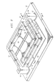
- FIG. 1 is a diagrammatic perspective view of an infrared detector 10 which can sense thermal energy and output electrical signals representative of a two-dimensional image of that sensed thermal energy.
- the infrared detector 10 includes a focal plane array 12 disposed on a substrate 16 .
- the substrate 16 includes an integrated circuit of a type which is commonly known as a read out integrated circuit (ROIC).
- the ROIC reads out the thermal information gathered by the focal plane array 12 .
- a thermal element 17 is provided on the side of the substrate 16 opposite from the focal plane array 12 , in order to serve as a form of controlled heat sink which maintains the integrated circuit substrate 16 at a substantially constant temperature which is predefined.
- the constant temperature prevents ambient or internally generated temperature gradients from affecting operation of the focal plane 12 , and thus provides a baseline with which the thermal energy impinging on the focal plane array 12 can be accurately measured.
- the focal plane 12 includes a plurality of thermal sensors or detector elements, one of which is designated by reference numeral 21 .
- the detector elements are arranged in a two-dimensional array, and each detector element 21 corresponds to a respective pixel in each image detected by the infrared detector 10 .
- the focal plane array 12 of the disclosed embodiment includes 76,800 detector elements 21 , which are arranged in a 320 by 240 array. For clarity, however, FIG. 1 diagrammatically depicts only about 140 detector elements. It will be recognized that the total number of detector elements 21 in the focal plane array 12 could be larger or smaller. Further, even though FIG.
- FIG. 1 shows the detector elements 21 arranged in a two-dimensional array, they could alternatively be arranged in a one-dimensional array, or could be provided at arbitrary locations that do not conform to a specific pattern. With reference to FIG. 2, one of the detector elements 21 of FIG. 1 will be described in more detail.
- FIG. 2 is a diagrammatic fragmentary perspective view of a portion of the integrated circuit substrate 16 , which has one of the detector elements 21 on it.
- the detector elements all have the same structural configuration, and therefore only one of them is illustrated and described here in detail.
- the substrate 16 has on an upper surface thereof two spaced electrical contacts or pads 31 and 32 , which are each electrically coupled in a not-illustrated manner to an ROIC that is implemented within the substrate 16 .
- Two electrically conductive aluminum posts 33 and 34 are each electrically coupled to and extend upwardly from a respective one of the contacts 31 and 32 .
- Two approximately L-shaped legs 37 and 38 each have one end supported on a respective one of the posts 33 and 34 .
- the legs 33 and 34 are multi-layered parts, as discussed later.
- the opposite ends of the legs 37 and 38 support a multi-layered membrane 41 , and the legs 37 and 38 each have other layers thereon, as described in more detail later.
- the top surface of the substrate 16 may optionally have thereon a layer 42 of a material which reflects infrared radiation.
- the distance between the membrane 41 and the reflective layer 42 is one-quarter wavelength, it may alternatively be some other appropriate distance, such as an odd multiple of one-quarter of a wavelength.
- FIG. 4 is a diagrammatic sectional view taken along the line 4 — 4 in FIG. 2
- FIG. 5 is a diagrammatic sectional view taken along the line 5 — 5 in FIG. 4 .
- the membrane 41 has several layers, including at the center a layer 51 of amorphous silicon.
- the layer 51 includes portions which extend out through each of the legs 37 and 38 to the region of the outer ends thereof.
- the amorphous silicon layer 51 has a thickness of approximately 300-700 ⁇ .
- the amorphous silicon 51 may be undoped, or may optionally have a small amount of p-type doping.
- TCR temperature coefficient of resistance
- TCR is a standard measure of the rate at which the resistance of the layer 51 will vary in response to a change in its temperature. TCR thus represents the sensitivity of the membrane 41 for purposes of detecting thermal radiation. A high value for TCR is desirable, in order to have a high level of sensitivity for purposes of detecting thermal radiation. Variation from no doping through low and medium-level doping to high-level doping permits the selection of a desired TCR value from a range of approximately 2.3 to 11.5%/K.
- an electrically conductive bottom electrode 53 On the underside of the amorphous silicon 51 is an electrically conductive bottom electrode 53 , which in the disclosed embodiment is substantially coextensive in length and width with the layer 51 , and which is not directly electrically coupled to any circuitry external to the membrane 41 .
- the layer 53 does not have portions which extend out through the legs 37 and 38 .
- Electrodes 56 and 57 are provided on the upper side of the layer 51 , and are each made from an electrically conductive material.
- the electrodes 56 and 57 are each made from a titanium and aluminum alloy with approximately 50% aluminum and 50% titanium, but the amounts of aluminum and titanium could alternatively be varied.
- the electrodes 56 and 57 are each of approximately rectangular shape, the nearest side edges thereof being spaced and parallel.
- the electrodes 53 and 56 - 57 are each in ohmic contact with the amorphous silicon 51 .
- Conductive strips 58 and 59 which technically are integral parts of the respective electrodes 56 and 57 , each extend from a respective one of the electrodes 56 and 57 out through a respective one of the legs 37 and 38 to a respective one of the posts 33 and 34 , where the strips 58 and 59 are respectively electrically coupled to the posts 33 and 34 .
- the strips 58 and 59 are made from the same material as the electrodes 56 and 57 . As best seen in FIG. 4, the strips 58 and 59 are each somewhat narrower in width than the associated leg 37 or 38 .
- the aluminum and titanium alloy used for the strips 58 - 59 and for the electrodes 53 and 56 - 57 is electrically conductive, but can also absorb infrared radiation where, as here, it is in the form of a layer which is sufficiently thin so that it tends to absorb rather than reflect the infrared radiation.
- the strips 58 - 59 and the electrodes 53 and 56 - 57 each have a thickness of approximately 100-200 ⁇ .
- the membrane 41 further includes bottom and top insulating layers 61 - 62 .
- the insulating layers 61 - 62 are made from a dielectric material such as silicon nitride (SiN), but they could alternatively be made from some other suitable insulating material.
- the bottom insulating layer 61 is provided on the underside of the electrode 53 , and is substantially coextensive in length and width with the electrode 53 .
- the top insulating layer 62 is provided on top of the electrodes 56 and 57 , and also in the region between them, and has substantially the same length and width as the bottom electrode 53 .
- the bottom insulating layer 61 has a thickness in the range of approximately 200-1000 ⁇ .
- the portion of the top insulating layer 62 above the electrodes 56 - 57 has a thickness in the range of approximately 200-1500 ⁇ .
- the top and bottom insulating layers 61 - 62 help rigidity the membrane 41 , so as to keep it approximately planar in view of the fact that it has no structural support directly beneath it. Further, the insulating layers 61 - 62 serve to passivate the metal surfaces of the electrodes 53 and 56 - 57 , so as to limit oxidation of these surfaces.
- the layers 61 - 62 each include a striplike portion that extends out through a respective one of the legs 37 - 38 to the outer end thereof.
- the effective resistance of the amorphous silicon layer 51 within the membrane 41 can be selected in a manner which is independent of the doping level. This is achieved by appropriately configuring the amorphous silicon layer 51 and also the size and positions of the electrodes 53 and 56 - 57 , so as to control the effective distance and area in the amorphous silicon through which current must pass as it flows between the electrodes.
- the amorphous silicon layer 51 can thus be configured to have no doping or low-level doping of the amorphous silicon layer 51 , in order to obtain a high TCR and a high level of sensitivity, while realizing a resistance which is selected independently of the doping so as to be in the range of approximately 10 K ⁇ to approximately 1000 K ⁇ .
- the effective resistance can be set to a selected value within a range of 30 M ⁇ -100 M ⁇ , which is compatible with integrating amplifiers of a known type that are used to detect and read out information present in the detector element 21 as a result of received thermal energy.
- the impedance of the detector element can be matched to an ROIC input impedance over a relatively wide range, while using little or no doping, in order to obtain a high TCR value.
- the electrodes 53 and 56 - 57 are made of an aluminum and titanium alloy, which has been selected because it can be deposited in a thickness where it absorbs infrared radiation while maintaining a usable direct current conductivity.
- the electrodes 53 and 56 - 57 can each directly absorb thermal radiation and deliver it to the amorphous silicon layer 51 , without any need for a special additional layer which is separate from the electrodes and which is provided solely for the purpose of absorbing infrared radiation.
- a dedicated absorber layer there is greater flexibility for structurally configuring the layer 51 and the electrodes 53 and 56 - 57 so as to achieve the desired resistance through the amorphous silicon layer 51 between the electrodes.
- FIG. 6 is a diagrammatic sectional view similar to FIG. 4, but showing a membrane 81 which is an alternative embodiment of the membrane 41 shown in FIGS. 2-5.
- the membrane 81 of FIG. 6 is generally similar to the membrane 41 , except that the bottom electrode shown at 53 in FIG. 4 has been omitted from the membrane 81 of FIG. 6 .
- the silicon layer 51 and the electrodes 56 - 57 are structurally configured with respect to each other so that the effective length and area in layer 51 which is subject to current flow provides an effective resistance for the membrane 81 which can be selected independently of the extent to which doping is or is not provided within the layer 51 .
- FIG. 7 is a diagrammatic view similar to FIG. 6, but showing a membrane 85 which is a further embodiment of the invention.
- FIG. 8 is a diagrammatic sectional top view similar to FIG. 5, but showing the membrane 85 of FIG. 7 .
- the membrane 85 of FIGS. 7 and 8 is similar to the membrane 81 of FIG. 6, except for the differences described below.
- the membrane 85 has on top of the layer 51 a pair of spaced layers 86 and 87 of an insulating material such as silicon nitride (SiN), with a strip 88 of this same insulating material disposed between and spaced from each of the layers 86 and 87 .
- the strip 88 is slightly wider than the distance between the adjacent edges of the electrodes 56 and 57 .
- the portions 86 - 88 of the insulating material each have a thickness of about 250-350 ⁇ .
- electrodes 56 and 57 are spaced by a distance of about 1 micron.
- the electrode 56 is in ohmic contact with the amorphous silicon layer 51 between the layer 86 and the strip 88
- the electrode 57 is in ohmic contact with the layer 51 between the layer 87 and the strip 88 .
- the inclusion of the silicon nitride portions 86 - 88 serves to enhance the rigidity of the membrane 85 .
- the layers 86 and 87 each include a portion which extends out to the end of a respective one of the legs 37 or 38 , and which has a respective trench 89 or 90 etched in it.
- the conductive strips 58 - 59 which are parts of the respective electrodes 56 - 57 are each disposed within a respective one of the trenches 89 - 90 .
- the conductive material of the strips 58 - 59 and the electrodes 56 - 57 is in ohmic contact with the top surface of the amorphous silicon layer 51 from the posts 33 - 34 all the way to the region between the insulating portions 86 and 88 and the region between the insulating portions 87 and 88 .
- the conductive material includes portions which extend from the posts to these regions without any sections or “steps” where the conductive material has to leave the layer 51 and travel over a part of the insulating portions 86 - 87 . Since the conductive material 56 - 59 has a thickness somewhat less than the thickness of the insulating portions 86 - 88 , the existence of such a step would make it more difficult to ensure continuous and relatively uniform thickness and conductivity of the conductive portions from the membrane all the way out to the posts 33 - 34 . The disclosed embodiment thus ensures that there is a continuous path out to each post without any such step, even though other parts of the conductive portions 56 - 57 are disposed on top of the insulating portions 86 - 88 .
- a layer of silicon nitride is deposited on the amorphous silicon layer 51 , and then a masked etch is carried out to expose selected portions of the layer 51 . This includes creation of the trenches 89 - 90 , and formation of the insulating portions 86 - 88 having trenches therebetween. Then, a layer of metalization is deposited over the resulting structure, and a further masked etch is carried out to define the electrodes 56 - 57 and the conductive strips 58 - 59 .
- FIG. 9 is a diagrammatic sectional view similar to FIG. 4, but showing a membrane 91 which is an alternative embodiment of the membrane 41 of FIG. 4 .
- the membrane 91 is generally similar to the membrane 41 , except as described below.
- the two electrodes 56 - 57 of the membrane 41 in FIG. 4 have been replaced with a single top electrode 92 in the membrane 91 , the electrode 92 having a length and width which are coextensive with the length and width of the amorphous silicon layer 51 and the bottom electrode 53 .
- the top electrode 92 is integral with a not-illustrated conductive strip, which is similar to the strip 58 (FIG. 5) and which extends out through the leg 37 to the post 33 .
- the bottom electrode 53 is integral with a conductive strip 94 , which extends out through the leg 38 to the post 34 .
- the layer 51 and the electrodes 53 and 92 are structurally configured so that the layer 51 provides the membrane 91 with a desired level of resistance, which is selected independently of any doping, and which can be selected to match the impedance of the membrane 91 to the input impedance of an associated ROIC circuit.
- FIGS. 10 and 11 show a further membrane 111 which is an alternative embodiment of the membrane 81 shown in FIG. 6 .
- FIG. 10 is a diagrammatic sectional view similar to FIG. 6, and
- FIG. 11 is a diagrammatic sectional view taken along the line 11 — 11 in FIG. 10 .
- FIG. 11 includes a section line 10 — 10 corresponding to the view of FIG. 10 .
- the membrane 111 is generally similar to the membrane 81 of FIG. 6, except as described below.
- the electrodes 56 and 57 in FIG. 6 have been replaced with two electrodes 112 and 113 that have a different configuration. As best seen in FIG.
- the electrode 112 has two fingers 116 and 117 , and the electrode 113 has a finger 118 which is disposed between the fingers 116 and 117 , in a manner so that there is an approximately uniform spacing between the electrodes 112 and 113 at almost all locations along the outer edge of the electrode 113 .
- the uniform spacing between the electrodes is approximately 1 micron.
- Two conductive strips 119 and 120 are each integral with a respective one of the electrodes 112 and 113 , and each extend through a respective one of the legs 37 and 38 to a respective one of the posts 33 - 34 .
- the strips 119 - 120 are each somewhat narrower than the associated leg 37 or 38 .
- the electrode 112 has two fingers and the electrode 113 has one finger in FIG. 10, the electrode 113 could have a larger number of fingers, and the electrode 112 could have a larger or smaller number of fingers, so long as the fingers of the two electrodes are interdigitated.
- the arrows 121 and 122 in FIG. 10 show how current can flow through the amorphous silicon layer 51 from the electrode 113 to the electrode 112 .
- the amorphous silicon layer 51 of the membrane 111 can be undoped or can be doped to a selected level, in order to provide the layer 51 with a desired TCR.
- the configuration of the electrodes 112 and 113 and the spacing between them is selected so that the amorphous silicon layer 51 provides between the electrodes 112 and 113 an effective resistance which has a desired value that has been selected independently of the TCR and any doping that may be present.
- FIGS. 12 and 13 show a membrane 123 , which is an alternative embodiment of the membrane 111 shown in FIGS. 10-11. More specifically, FIG. 12 is a diagrammatic sectional view similar to FIG. 10, and FIG. 13 is a diagrammatic sectional view similar to FIG. 11 .
- the membrane 123 of FIGS. 12-13 is generally similar to the membrane 111 of FIGS. 10-11, except for the differences described below.
- a layer of an insulating material such as silicon nitride is deposited on the amorphous silicon layer 51 with a thickness of about 250-350 ⁇ , and is then etched to create four separate portions 124 - 127 , which are indicated in FIG. 12 by broken lines.
- This etching step includes the creation of trenches 129 - 130 through the insulating material which is in the legs 37 - 38 .
- a metalization layer is then deposited, and is etched to create two electrodes 131 - 132 , and associated conductive strips in the respective trenches 129 - 130 , one of the conductive strips being visible at 133 in FIG. 12 .
- the insulating layer 62 is then deposited over the resulting structure.
- the adjacent edges of the electrodes 131 - 132 are spaced by a distance of approximately 1 micron.
- the electrodes 131 - 132 have interdigitated fingers, including two spaced fingers 134 - 135 (FIG. 13) which are part of the electrode 131 , and one finger 138 (FIG. 13) which is part of the electrode 132 and which is disposed between the fingers 134 - 135 .
- the electrode 131 contacts the amorphous silicon layer 51 through a trench which is defined by the region between the insulating portion 125 and the insulating portions 126 - 127
- the electrode 132 contacts the amorphous silicon layer 51 through a further trench which is defined by the region between the insulating portion 124 and the insulating portion 125 .
- the width of the insulating portion 125 determines the distance which current must flow through the amorphous silicon layer 51 , and thus determines the resistivity of the membrane 123 .
- the combined area of the electrodes 131 - 132 covers substantially the entire membrane, except primarily for the gap between their adjacent edges.
- each electrode can efficiently absorb infrared radiation across its entire area, while the area of contact between each electrode and the amorphous silicon layer 51 is much smaller and can be controlled in size and placement through control of the width and placement of the trench between the insulating portions 125 and 126 - 127 or the trench between the insulating portions 124 - 125 .
- FIG. 15 is a diagrammatic sectional side view of the membrane 141 taken along the line 15 — 15 in FIG. 14
- FIG. 16 is a diagrammatic sectional plan view taken along the line 16 — 16 in FIG. 15
- FIG. 17 is a diagrammatic sectional side view taken along the line 17 — 17 in FIG. 16 .
- FIG. 17 also diagrammatically depicts the reflective layer 42 .
- FIG. 17 is not to scale.
- the membrane 141 is a multi-layer member, where the arrangement of layers in a vertical direction is generally similar to that shown in FIG. 4 .
- the amorphous silicon layer 142 and the electrodes 143 - 145 are sandwiched between top and bottom insulating layers 146 and 147 .
- the thicknesses and materials used for the elements 142 - 147 are the same as the thicknesses and materials used for the corresponding elements in the embodiment of FIG. 4 .
- the legs 136 and 137 each have multiple layers corresponding to respective layers of the membrane 141 , except that neither leg has a layer corresponding to the bottom electrode 143 .
- the membrane 141 of FIGS. 14-17 has 16 openings 149 provided through it, in a pattern which forms a four-by-four array of openings. Due to the presence of the openings, the membrane 141 may be viewed as having five spaced and parallel strips 151 - 155 that extend in one direction, and three spaced and parallel strips 156 - 158 that extend from the strip 151 to the strip 155 in a direction perpendicular to the strips 151 - 155 .
- FIG. 14 provides a good view of the electrodes 144 and 145 , along with a portion of the insulating layer 147 which is disposed between these electrodes. In the embodiment of FIGS.
- the legs 136 and 137 each have a width of approximately 0.75 ⁇ m
- the strips 151 - 158 each have a width of approximately 1.25 ⁇ m.
- the distance 171 between the centers of any two adjacent strips 151 - 158 is approximately 5.75 ⁇ m.
- the vertical distance between the reflective layer 42 and the membrane 141 is approximately 2.5 ⁇ m, which is approximately one-quarter of a wavelength of the infrared radiation of interest.
- the distance between the membrane 141 and the reflective layer 42 is one-quarter wavelength, it may alternatively be some other appropriate distance, such as an odd multiple of one-quarter of a wavelength.
- FIG. 4 A brief description will now be provided of the operation of the disclosed embodiments, beginning with the embodiment of FIGS. 1-5.
- arriving infrared radiation will impinge on the top surface of the membrane 41 , as indicated diagrammatically by arrow 162 .
- a small portion of this radiation may be reflected, as indicated diagrammatically by arrow 163 .
- most of the radiation 162 will travel into the membrane 41 , where it will be absorbed by one of the electrodes 53 or 56 - 57 .
- These electrodes transfer absorbed thermal energy to the amorphous silicon layer 51 .
- the resistance provided by this layer between the electrodes 56 and 53 and between the electrodes 53 and 57 will vary at rate corresponding to the TRC. Consequently, by measuring the cumulative resistance currently provided by the amorphous silicon layer 51 between the electrodes 56 - 57 , an external ROIC disposed in the substrate 16 (FIG. 2) can determine the amount of thermal energy which has been absorbed by the membrane 41 .
- the thermal energy 162 which enters the membrane 41 may pass entirely through the membrane 41 . With reference to FIG. 2, it will then be reflected by the reflective layer 42 .
- the distance between membrane 41 and reflective layer 42 has been selected to be approximately one-quarter of a wavelength of the infrared radiation of interest.
- the space between the membrane 41 and the reflective layer 42 forms a resonant cavity which effectively traps this radiation until it travels upwardly back into the membrane 41 , where it is absorbed by the electrodes.
- the distance between the membrane 41 and the reflective layer 42 is one-quarter wavelength, it may alternatively be some other appropriate distance, such as an odd multiple of one-quarter of a wavelength.
- energy from the incident radiation 179 is diffracted by the cross-grating membrane 141 into higher order, non-propagating evanescent cavity modes, which appear within the diffractive resonant cavity.
- the radiation 179 which initially passes through the membrane 141 will be trapped within the resonant cavity until it is absorbed by one of the strips 151 - 158 .
- operation of the embodiment of FIGS. 14-17 is generally similar to the operation described above for the embodiment of FIGS. 1-5. It will be recognized that the embodiment of FIGS. 14-17 is capable of absorbing infrared radiation approximately as efficiently as the embodiment of FIGS. 1-5, but has a much smaller physical and thermal mass. Due to the reduced thermal mass, it is possible to achieve a low thermal time constant, for example less than 5 msec.
- amorphous silicon based detector elements This permits pixel impedance to be matched to ROIC impedance over a wide range, thereby permitting amorphous silicon based detector elements to be used with existing ROIC circuits, including pulsed-bias mode current skimming ROIC designs commonly used with vanadium oxide detector elements, as well as direct current bias switched capacitor integrating amplifier per unit cell ROIC designs.
- a further advantage is that the mass of the membrane of each detector element is reduced, which increases pixel response by lowering the thermal mass, at no cost to absorption efficiency. As such, a very low thermal time constant is realized, which in turn contributes to a relatively high operating speed, for example up to a 100 Hz frame rate using an f/1 optical system.
- a further advantage results from the implementation of the electrodes with a material which is electrically conductive and which can also absorb thermal radiation, thereby avoiding the need for a separate layer or element which is dedicated to absorbing thermal radiation within the membrane.
Abstract
Description
Claims (38)
Priority Applications (3)
| Application Number | Priority Date | Filing Date | Title |
|---|---|---|---|
| US09/844,171 US6777681B1 (en) | 2001-04-25 | 2001-04-25 | Infrared detector with amorphous silicon detector elements, and a method of making it |
| PCT/US2002/009781 WO2002088648A1 (en) | 2001-04-25 | 2002-03-28 | Infrared detector with amorphous silicon detector elements, and a method of making it |
| EP02725419A EP1381835A1 (en) | 2001-04-25 | 2002-03-28 | Infrared detector with amorphous silicon detector elements, and a method of making it |
Applications Claiming Priority (1)
| Application Number | Priority Date | Filing Date | Title |
|---|---|---|---|
| US09/844,171 US6777681B1 (en) | 2001-04-25 | 2001-04-25 | Infrared detector with amorphous silicon detector elements, and a method of making it |
Publications (1)
| Publication Number | Publication Date |
|---|---|
| US6777681B1 true US6777681B1 (en) | 2004-08-17 |
Family
ID=25292016
Family Applications (1)
| Application Number | Title | Priority Date | Filing Date |
|---|---|---|---|
| US09/844,171 Expired - Lifetime US6777681B1 (en) | 2001-04-25 | 2001-04-25 | Infrared detector with amorphous silicon detector elements, and a method of making it |
Country Status (3)
| Country | Link |
|---|---|
| US (1) | US6777681B1 (en) |
| EP (1) | EP1381835A1 (en) |
| WO (1) | WO2002088648A1 (en) |
Cited By (23)
| Publication number | Priority date | Publication date | Assignee | Title |
|---|---|---|---|---|
| US20050269512A1 (en) * | 2004-05-24 | 2005-12-08 | Nec Electronics Corporation | Semiconductor device including vanadium oxide sensor element with restricted current density |
| US20060060784A1 (en) * | 2004-09-17 | 2006-03-23 | Korea Institute Of Science And Technology | Infrared absorption layer structure and its formation method, and an uncooled infrared detector using this structure |
| US20060124831A1 (en) * | 2004-12-10 | 2006-06-15 | Schimert Thomas R | Optically blocked reference pixels for focal plane arrays |
| US20060202120A1 (en) * | 2005-03-14 | 2006-09-14 | Kauffman Christopher L | Photoconductive bolometer infrared detector |
| US20060271522A1 (en) * | 2005-05-31 | 2006-11-30 | Microsoft Corporation | Predictive phonetic data search |
| US20070170360A1 (en) * | 2006-01-26 | 2007-07-26 | Gooch Roland W | Systems and methods for bonding |
| US20070170359A1 (en) * | 2006-01-26 | 2007-07-26 | Syllaios Athanasios J | Systems and methods for integrating focal plane arrays |
| US20070170363A1 (en) * | 2006-01-26 | 2007-07-26 | Schimert Thomas R | Infrared detector elements and methods of forming same |
| US20080048120A1 (en) * | 2006-08-28 | 2008-02-28 | Gooch Roland W | Surface mounted infrared image detector systems and associated methods |
| CN100380587C (en) * | 2006-07-31 | 2008-04-09 | 西安工业大学 | Method for producing amorphous silicon thermal imaging detector micro-structure with self-supporting |
| US7442933B2 (en) | 2005-02-03 | 2008-10-28 | Lin Alice L | Bolometer having an amorphous titanium oxide layer with high resistance stability |
| US20090140147A1 (en) * | 2007-08-22 | 2009-06-04 | Skidmore George D | Pixel structure having an umbrella type absorber with one or more recesses or channels sized to increase radiation absorption |
| US7718965B1 (en) | 2006-08-03 | 2010-05-18 | L-3 Communications Corporation | Microbolometer infrared detector elements and methods for forming same |
| US20100265078A1 (en) * | 2009-04-20 | 2010-10-21 | Integrated Sensors, Llc | Plasma panel based ionizing-particle radiation detector |
| US20120018636A1 (en) * | 2009-03-31 | 2012-01-26 | Panasonic Electric Works Co., Ltd. | Infrared array sensor |
| US8153980B1 (en) | 2006-11-30 | 2012-04-10 | L-3 Communications Corp. | Color correction for radiation detectors |
| US8227755B2 (en) | 2010-04-28 | 2012-07-24 | L-3 Communications Corporation | Pixel-level optically transitioning filter elements for detector devices |
| DE112011101491T5 (en) | 2010-04-28 | 2013-04-04 | L-3 Communications Corp. | Optically changing thermal detector structures |
| DE112011101492T5 (en) | 2010-04-28 | 2013-05-29 | L-3 Communications Corporation | Pixel structure for microbolometer detector |
| US8610070B2 (en) | 2010-04-28 | 2013-12-17 | L-3 Communications Corporation | Pixel-level optical elements for uncooled infrared detector devices |
| US20140151557A1 (en) * | 2012-12-03 | 2014-06-05 | Analog Devices, Inc. | Photonic sensor and a method of manufacturing such a sensor |
| US8765514B1 (en) | 2010-11-12 | 2014-07-01 | L-3 Communications Corp. | Transitioned film growth for conductive semiconductor materials |
| US20160003677A1 (en) * | 2013-03-15 | 2016-01-07 | Polaris Sensor Technologies, Inc. | Long wave infrared imaging polarimeter, and method of assembly |
Families Citing this family (2)
| Publication number | Priority date | Publication date | Assignee | Title |
|---|---|---|---|---|
| US7633065B2 (en) * | 2006-10-19 | 2009-12-15 | Sensormatic Electronics, LLC | Conduction structure for infrared microbolometer sensors |
| US7842533B2 (en) | 2009-01-07 | 2010-11-30 | Robert Bosch Gmbh | Electromagnetic radiation sensor and method of manufacture |
Citations (68)
| Publication number | Priority date | Publication date | Assignee | Title |
|---|---|---|---|---|
| US4169273A (en) | 1978-06-26 | 1979-09-25 | Honeywell Inc. | Photodetector signal processing |
| US4291815A (en) | 1980-02-19 | 1981-09-29 | Consolidated Refining Co., Inc. | Ceramic lid assembly for hermetic sealing of a semiconductor chip |
| US4352449A (en) | 1979-12-26 | 1982-10-05 | Bell Telephone Laboratories, Incorporated | Fabrication of circuit packages |
| US4654622A (en) | 1985-09-30 | 1987-03-31 | Honeywell Inc. | Monolithic integrated dual mode IR/mm-wave focal plane sensor |
| US4701424A (en) | 1986-10-30 | 1987-10-20 | Ford Motor Company | Hermetic sealing of silicon |
| US4752694A (en) | 1987-01-12 | 1988-06-21 | Honeywell Inc. | Array uniformity correction |
| US5010251A (en) | 1988-08-04 | 1991-04-23 | Hughes Aircraft Company | Radiation detector array using radiation sensitive bridges |
| US5021663A (en) | 1988-08-12 | 1991-06-04 | Texas Instruments Incorporated | Infrared detector |
| US5082162A (en) | 1990-02-05 | 1992-01-21 | Matsushita Electric Industrial Co., Ltd. | Methods for soldering semiconductor devices |
| US5196377A (en) | 1990-12-20 | 1993-03-23 | Cray Research, Inc. | Method of fabricating silicon-based carriers |
| US5220188A (en) | 1983-07-06 | 1993-06-15 | Honeywell Inc. | Integrated micromechanical sensor element |
| US5260225A (en) | 1991-12-20 | 1993-11-09 | Honeywell Inc. | Integrated infrared sensitive bolometers |
| US5286671A (en) | 1993-05-07 | 1994-02-15 | Kulite Semiconductor Products, Inc. | Fusion bonding technique for use in fabricating semiconductor devices |
| US5286976A (en) | 1988-11-07 | 1994-02-15 | Honeywell Inc. | Microstructure design for high IR sensitivity |
| US5288649A (en) | 1991-09-30 | 1994-02-22 | Texas Instruments Incorporated | Method for forming uncooled infrared detector |
| US5300915A (en) | 1986-07-16 | 1994-04-05 | Honeywell Inc. | Thermal sensor |
| US5367194A (en) | 1990-10-29 | 1994-11-22 | Hewlett-Packard Company | Microchip assembly with electrical element in sealed cavity |
| US5431328A (en) | 1994-05-06 | 1995-07-11 | Industrial Technology Research Institute | Composite bump flip chip bonding |
| US5449910A (en) | 1993-11-17 | 1995-09-12 | Honeywell Inc. | Infrared radiation imaging array with compound sensors forming each pixel |
| US5450053A (en) | 1985-09-30 | 1995-09-12 | Honeywell Inc. | Use of vanadium oxide in microbolometer sensors |
| US5455421A (en) | 1985-08-13 | 1995-10-03 | Massachusetts Institute Of Technology | Infrared detector using a resonant optical cavity for enhanced absorption |
| US5512748A (en) | 1994-07-26 | 1996-04-30 | Texas Instruments Incorporated | Thermal imaging system with a monolithic focal plane array and method |
| US5534111A (en) | 1988-02-29 | 1996-07-09 | Honeywell Inc. | Thermal isolation microstructure |
| US5539206A (en) | 1995-04-20 | 1996-07-23 | Loral Vought Systems Corporation | Enhanced quantum well infrared photodetector |
| US5573859A (en) | 1995-09-05 | 1996-11-12 | Motorola, Inc. | Auto-regulating solder composition |
| US5589688A (en) * | 1994-11-30 | 1996-12-31 | Terumo Kabushiki Kaisha | Infrared radiation sensor |
| US5605489A (en) | 1993-06-24 | 1997-02-25 | Texas Instruments Incorporated | Method of protecting micromechanical devices during wafer separation |
| US5659195A (en) | 1995-06-08 | 1997-08-19 | The Regents Of The University Of California | CMOS integrated microsensor with a precision measurement circuit |
| US5701008A (en) | 1996-11-29 | 1997-12-23 | He Holdings, Inc. | Integrated infrared microlens and gas molecule getter grating in a vacuum package |
| US5726480A (en) | 1995-01-27 | 1998-03-10 | The Regents Of The University Of California | Etchants for use in micromachining of CMOS Microaccelerometers and microelectromechanical devices and method of making the same |
| EP0828346A2 (en) | 1996-08-29 | 1998-03-11 | Harris Corporation | Lid wafer bond packaging and micromachining |
| US5760398A (en) | 1995-12-04 | 1998-06-02 | Lockheed Martin Ir Imaging Systems, Inc. | Infrared radiation detector having a reduced active area |
| US5773987A (en) | 1996-02-26 | 1998-06-30 | Motorola, Inc. | Method for probing a semiconductor wafer using a motor controlled scrub process |
| US5777328A (en) | 1995-07-21 | 1998-07-07 | Texas Instruments Incorporated | Ramped foot support |
| US5789753A (en) | 1995-07-21 | 1998-08-04 | Texas Instruments Incorporated | Stress tolerant bolometer |
| US5825029A (en) * | 1995-06-15 | 1998-10-20 | Commissariat A L'energie Atomique | Bolometric detection device for millimeter and sub-millimeter waves and a method for manufacturing this device |
| US5895233A (en) | 1993-12-13 | 1999-04-20 | Honeywell Inc. | Integrated silicon vacuum micropackage for infrared devices |
| US5905007A (en) | 1997-08-01 | 1999-05-18 | The Regents Of The University Of California | Method for aligning and forming microelectromechanical systems (MEMS) contour surfaces |
| US5912464A (en) * | 1996-08-08 | 1999-06-15 | Commissariat Al'energie Atomique | Infrared detector and manufacturing process |
| US5919548A (en) | 1996-10-11 | 1999-07-06 | Sandia Corporation | Chemical-mechanical polishing of recessed microelectromechanical devices |
| US5921461A (en) | 1997-06-11 | 1999-07-13 | Raytheon Company | Vacuum package having vacuum-deposited local getter and its preparation |
| US5923995A (en) | 1997-04-18 | 1999-07-13 | National Semiconductor Corporation | Methods and apparatuses for singulation of microelectromechanical systems |
| US5929441A (en) | 1997-06-27 | 1999-07-27 | Texas Instruments Incorporated | Low mass optical coating for thin film detectors |
| US5945673A (en) | 1996-08-30 | 1999-08-31 | Raytheon Company | Thermal detector with nucleation element and method |
| WO1999050905A1 (en) | 1998-03-31 | 1999-10-07 | Honeywell Inc. | Wafer-pair having deposited layer sealed chambers |
| US5970315A (en) | 1995-07-21 | 1999-10-19 | Carnegie Mellon University | Microelectromechanical structure and process of making same |
| EP0951069A1 (en) | 1998-04-17 | 1999-10-20 | Interuniversitair Microelektronica Centrum Vzw | Method of fabrication of a microstructure having an inside cavity |
| FR2780200A1 (en) | 1998-06-22 | 1999-12-24 | Commissariat Energie Atomique | Sealed cavity for electronic or electromagnetic component |
| EP0971219A1 (en) | 1998-07-06 | 2000-01-12 | Commissariat A L'energie Atomique | Thermal detektor with amplication by bolometric effect |
| EP0977275A1 (en) | 1998-07-28 | 2000-02-02 | Commissariat A L'energie Atomique | Infrared/visible multispectral radiation detector |
| US6028312A (en) | 1995-07-21 | 2000-02-22 | Texas Instruments Incorporated | Electronic chopping |
| US6036872A (en) | 1998-03-31 | 2000-03-14 | Honeywell Inc. | Method for making a wafer-pair having sealed chambers |
| US6046067A (en) | 1993-09-27 | 2000-04-04 | Siemens Aktiengesellschaft | Micromechanical device and method for its production |
| US6054745A (en) | 1999-01-04 | 2000-04-25 | International Business Machines Corporation | Nonvolatile memory cell using microelectromechanical device |
| US6064216A (en) | 1996-12-31 | 2000-05-16 | Micron Technology, Inc. | Apparatus for testing semiconductor wafers |
| US6062461A (en) | 1998-06-03 | 2000-05-16 | Delphi Technologies, Inc. | Process for bonding micromachined wafers using solder |
| US6087199A (en) | 1998-02-04 | 2000-07-11 | International Business Machines Corporation | Method for fabricating a very dense chip package |
| US6100525A (en) | 1986-07-14 | 2000-08-08 | Lockheed Martin Corporation | Uncooled infrared detector |
| US6111254A (en) | 1986-07-14 | 2000-08-29 | Lockheed Martin Corporation | Infrared radiation detector |
| US6114697A (en) | 1986-07-14 | 2000-09-05 | Lockheed Martin Corporation | Bandgap radiation detector |
| US6119920A (en) | 1996-12-20 | 2000-09-19 | Rf Monolithics, Inc. | Method of forming an electronic package with a solder seal |
| US6133570A (en) | 1994-03-15 | 2000-10-17 | Lockheed Martin Corporation | Semiconductor photovoltaic diffractive resonant optical cavity infrared detector |
| US6143997A (en) | 1999-06-04 | 2000-11-07 | The Board Of Trustees Of The University Of Illinois | Low actuation voltage microelectromechanical device and method of manufacture |
| US6159812A (en) | 1998-02-06 | 2000-12-12 | Advanced Micro Devices, Inc. | Reduced boron diffusion by use of a pre-anneal |
| EP1072875A1 (en) | 1999-07-26 | 2001-01-31 | Nec Corporation | Infrared detector array with microbridge stucrure |
| US6210988B1 (en) | 1999-01-15 | 2001-04-03 | The Regents Of The University Of California | Polycrystalline silicon germanium films for forming micro-electromechanical systems |
| US6232150B1 (en) | 1998-12-03 | 2001-05-15 | The Regents Of The University Of Michigan | Process for making microstructures and microstructures made thereby |
| US6392232B1 (en) | 1995-07-21 | 2002-05-21 | Pharmarcopeia, Inc. | High fill factor bolometer array |
-
2001
- 2001-04-25 US US09/844,171 patent/US6777681B1/en not_active Expired - Lifetime
-
2002
- 2002-03-28 WO PCT/US2002/009781 patent/WO2002088648A1/en not_active Application Discontinuation
- 2002-03-28 EP EP02725419A patent/EP1381835A1/en not_active Withdrawn
Patent Citations (75)
| Publication number | Priority date | Publication date | Assignee | Title |
|---|---|---|---|---|
| US4169273A (en) | 1978-06-26 | 1979-09-25 | Honeywell Inc. | Photodetector signal processing |
| US4352449A (en) | 1979-12-26 | 1982-10-05 | Bell Telephone Laboratories, Incorporated | Fabrication of circuit packages |
| US4291815B1 (en) | 1980-02-19 | 1998-09-29 | Semiconductor Packaging Materi | Ceramic lid assembly for hermetic sealing of a semiconductor chip |
| US4291815A (en) | 1980-02-19 | 1981-09-29 | Consolidated Refining Co., Inc. | Ceramic lid assembly for hermetic sealing of a semiconductor chip |
| US5220188A (en) | 1983-07-06 | 1993-06-15 | Honeywell Inc. | Integrated micromechanical sensor element |
| US5455421A (en) | 1985-08-13 | 1995-10-03 | Massachusetts Institute Of Technology | Infrared detector using a resonant optical cavity for enhanced absorption |
| US4654622A (en) | 1985-09-30 | 1987-03-31 | Honeywell Inc. | Monolithic integrated dual mode IR/mm-wave focal plane sensor |
| US5450053A (en) | 1985-09-30 | 1995-09-12 | Honeywell Inc. | Use of vanadium oxide in microbolometer sensors |
| US6111254A (en) | 1986-07-14 | 2000-08-29 | Lockheed Martin Corporation | Infrared radiation detector |
| US6114697A (en) | 1986-07-14 | 2000-09-05 | Lockheed Martin Corporation | Bandgap radiation detector |
| US6100525A (en) | 1986-07-14 | 2000-08-08 | Lockheed Martin Corporation | Uncooled infrared detector |
| US6114696A (en) | 1986-07-14 | 2000-09-05 | Lockheed Martin Corporation | Uncooled infrared detector |
| US5300915A (en) | 1986-07-16 | 1994-04-05 | Honeywell Inc. | Thermal sensor |
| US4701424A (en) | 1986-10-30 | 1987-10-20 | Ford Motor Company | Hermetic sealing of silicon |
| US4752694A (en) | 1987-01-12 | 1988-06-21 | Honeywell Inc. | Array uniformity correction |
| US5534111A (en) | 1988-02-29 | 1996-07-09 | Honeywell Inc. | Thermal isolation microstructure |
| US5010251A (en) | 1988-08-04 | 1991-04-23 | Hughes Aircraft Company | Radiation detector array using radiation sensitive bridges |
| US5021663A (en) | 1988-08-12 | 1991-06-04 | Texas Instruments Incorporated | Infrared detector |
| US5021663B1 (en) | 1988-08-12 | 1997-07-01 | Texas Instruments Inc | Infrared detector |
| US5286976A (en) | 1988-11-07 | 1994-02-15 | Honeywell Inc. | Microstructure design for high IR sensitivity |
| US5082162A (en) | 1990-02-05 | 1992-01-21 | Matsushita Electric Industrial Co., Ltd. | Methods for soldering semiconductor devices |
| US5367194A (en) | 1990-10-29 | 1994-11-22 | Hewlett-Packard Company | Microchip assembly with electrical element in sealed cavity |
| US5196377A (en) | 1990-12-20 | 1993-03-23 | Cray Research, Inc. | Method of fabricating silicon-based carriers |
| US5367167A (en) | 1991-09-30 | 1994-11-22 | Texas Instruments Incorporated | Uncooled infrared detector and method for forming the same |
| US5288649A (en) | 1991-09-30 | 1994-02-22 | Texas Instruments Incorporated | Method for forming uncooled infrared detector |
| US5260225A (en) | 1991-12-20 | 1993-11-09 | Honeywell Inc. | Integrated infrared sensitive bolometers |
| US5286671A (en) | 1993-05-07 | 1994-02-15 | Kulite Semiconductor Products, Inc. | Fusion bonding technique for use in fabricating semiconductor devices |
| US5605489A (en) | 1993-06-24 | 1997-02-25 | Texas Instruments Incorporated | Method of protecting micromechanical devices during wafer separation |
| US6046067A (en) | 1993-09-27 | 2000-04-04 | Siemens Aktiengesellschaft | Micromechanical device and method for its production |
| US5449910A (en) | 1993-11-17 | 1995-09-12 | Honeywell Inc. | Infrared radiation imaging array with compound sensors forming each pixel |
| US5895233A (en) | 1993-12-13 | 1999-04-20 | Honeywell Inc. | Integrated silicon vacuum micropackage for infrared devices |
| US6133570A (en) | 1994-03-15 | 2000-10-17 | Lockheed Martin Corporation | Semiconductor photovoltaic diffractive resonant optical cavity infrared detector |
| US5431328A (en) | 1994-05-06 | 1995-07-11 | Industrial Technology Research Institute | Composite bump flip chip bonding |
| US5512748A (en) | 1994-07-26 | 1996-04-30 | Texas Instruments Incorporated | Thermal imaging system with a monolithic focal plane array and method |
| US5589688A (en) * | 1994-11-30 | 1996-12-31 | Terumo Kabushiki Kaisha | Infrared radiation sensor |
| US5726480A (en) | 1995-01-27 | 1998-03-10 | The Regents Of The University Of California | Etchants for use in micromachining of CMOS Microaccelerometers and microelectromechanical devices and method of making the same |
| US5539206A (en) | 1995-04-20 | 1996-07-23 | Loral Vought Systems Corporation | Enhanced quantum well infrared photodetector |
| US5659195A (en) | 1995-06-08 | 1997-08-19 | The Regents Of The University Of California | CMOS integrated microsensor with a precision measurement circuit |
| US5825029A (en) * | 1995-06-15 | 1998-10-20 | Commissariat A L'energie Atomique | Bolometric detection device for millimeter and sub-millimeter waves and a method for manufacturing this device |
| US5777328A (en) | 1995-07-21 | 1998-07-07 | Texas Instruments Incorporated | Ramped foot support |
| US6028312A (en) | 1995-07-21 | 2000-02-22 | Texas Instruments Incorporated | Electronic chopping |
| US6392232B1 (en) | 1995-07-21 | 2002-05-21 | Pharmarcopeia, Inc. | High fill factor bolometer array |
| US5970315A (en) | 1995-07-21 | 1999-10-19 | Carnegie Mellon University | Microelectromechanical structure and process of making same |
| US5789753A (en) | 1995-07-21 | 1998-08-04 | Texas Instruments Incorporated | Stress tolerant bolometer |
| US5573859A (en) | 1995-09-05 | 1996-11-12 | Motorola, Inc. | Auto-regulating solder composition |
| US5760398A (en) | 1995-12-04 | 1998-06-02 | Lockheed Martin Ir Imaging Systems, Inc. | Infrared radiation detector having a reduced active area |
| US5773987A (en) | 1996-02-26 | 1998-06-30 | Motorola, Inc. | Method for probing a semiconductor wafer using a motor controlled scrub process |
| US5912464A (en) * | 1996-08-08 | 1999-06-15 | Commissariat Al'energie Atomique | Infrared detector and manufacturing process |
| US5915168A (en) | 1996-08-29 | 1999-06-22 | Harris Corporation | Lid wafer bond packaging and micromachining |
| EP0828346A2 (en) | 1996-08-29 | 1998-03-11 | Harris Corporation | Lid wafer bond packaging and micromachining |
| US5945673A (en) | 1996-08-30 | 1999-08-31 | Raytheon Company | Thermal detector with nucleation element and method |
| US5919548A (en) | 1996-10-11 | 1999-07-06 | Sandia Corporation | Chemical-mechanical polishing of recessed microelectromechanical devices |
| US5701008A (en) | 1996-11-29 | 1997-12-23 | He Holdings, Inc. | Integrated infrared microlens and gas molecule getter grating in a vacuum package |
| US6119920A (en) | 1996-12-20 | 2000-09-19 | Rf Monolithics, Inc. | Method of forming an electronic package with a solder seal |
| US6064216A (en) | 1996-12-31 | 2000-05-16 | Micron Technology, Inc. | Apparatus for testing semiconductor wafers |
| US5923995A (en) | 1997-04-18 | 1999-07-13 | National Semiconductor Corporation | Methods and apparatuses for singulation of microelectromechanical systems |
| US5921461A (en) | 1997-06-11 | 1999-07-13 | Raytheon Company | Vacuum package having vacuum-deposited local getter and its preparation |
| US5929441A (en) | 1997-06-27 | 1999-07-27 | Texas Instruments Incorporated | Low mass optical coating for thin film detectors |
| US5905007A (en) | 1997-08-01 | 1999-05-18 | The Regents Of The University Of California | Method for aligning and forming microelectromechanical systems (MEMS) contour surfaces |
| US6087199A (en) | 1998-02-04 | 2000-07-11 | International Business Machines Corporation | Method for fabricating a very dense chip package |
| US6159812A (en) | 1998-02-06 | 2000-12-12 | Advanced Micro Devices, Inc. | Reduced boron diffusion by use of a pre-anneal |
| US6036872A (en) | 1998-03-31 | 2000-03-14 | Honeywell Inc. | Method for making a wafer-pair having sealed chambers |
| WO1999050905A1 (en) | 1998-03-31 | 1999-10-07 | Honeywell Inc. | Wafer-pair having deposited layer sealed chambers |
| EP0951069A1 (en) | 1998-04-17 | 1999-10-20 | Interuniversitair Microelektronica Centrum Vzw | Method of fabrication of a microstructure having an inside cavity |
| US6062461A (en) | 1998-06-03 | 2000-05-16 | Delphi Technologies, Inc. | Process for bonding micromachined wafers using solder |
| FR2780200A1 (en) | 1998-06-22 | 1999-12-24 | Commissariat Energie Atomique | Sealed cavity for electronic or electromagnetic component |
| US6316770B1 (en) | 1998-07-06 | 2001-11-13 | Commissariat A L'energie Atomique | Thermal detector with bolometric effect amplification |
| EP0971219A1 (en) | 1998-07-06 | 2000-01-12 | Commissariat A L'energie Atomique | Thermal detektor with amplication by bolometric effect |
| EP0977275A1 (en) | 1998-07-28 | 2000-02-02 | Commissariat A L'energie Atomique | Infrared/visible multispectral radiation detector |
| US6320189B1 (en) | 1998-07-28 | 2001-11-20 | Commissariat A L'energie Atomique | Device for the detection of multispectral infrared/visible radiation |
| US6232150B1 (en) | 1998-12-03 | 2001-05-15 | The Regents Of The University Of Michigan | Process for making microstructures and microstructures made thereby |
| US6054745A (en) | 1999-01-04 | 2000-04-25 | International Business Machines Corporation | Nonvolatile memory cell using microelectromechanical device |
| US6210988B1 (en) | 1999-01-15 | 2001-04-03 | The Regents Of The University Of California | Polycrystalline silicon germanium films for forming micro-electromechanical systems |
| US6143997A (en) | 1999-06-04 | 2000-11-07 | The Board Of Trustees Of The University Of Illinois | Low actuation voltage microelectromechanical device and method of manufacture |
| EP1072875A1 (en) | 1999-07-26 | 2001-01-31 | Nec Corporation | Infrared detector array with microbridge stucrure |
Non-Patent Citations (2)
| Title |
|---|
| Tissot, et al., "LETI/LIR's Amorphous Silicon Uncooled Microbolometer Development", SPIE vol. 3379, Part of the SPIE Conference on Infrared Detectors and Focal Plane Arrays V, Orlando, Florida, Apr. 1998, pp. 139-144. |
| U.S. Ser. No. 09/557,748, "Microbolometer and Method for Forming", filed Apr. 25, 2000, inventors: Thomas R. Schimert, Roland W. Gooch, William McCardel and Bobbi A. Ritchey (Attorney Docket Nos. 004578. PD99E943). |
Cited By (46)
| Publication number | Priority date | Publication date | Assignee | Title |
|---|---|---|---|---|
| US20090212385A1 (en) * | 2004-05-24 | 2009-08-27 | Nec Electronics Corporation | Semiconductor device including vanadium oxide sensor element with restricted current density |
| US7544940B2 (en) * | 2004-05-24 | 2009-06-09 | Nec Electronics Corporation | Semiconductor device including vanadium oxide sensor element with restricted current density |
| US20050269512A1 (en) * | 2004-05-24 | 2005-12-08 | Nec Electronics Corporation | Semiconductor device including vanadium oxide sensor element with restricted current density |
| US7268349B2 (en) * | 2004-09-17 | 2007-09-11 | Korea Advanced Institute Of Science And Technology | Infrared absorption layer structure and its formation method, and an uncooled infrared detector using this structure |
| US20060060784A1 (en) * | 2004-09-17 | 2006-03-23 | Korea Institute Of Science And Technology | Infrared absorption layer structure and its formation method, and an uncooled infrared detector using this structure |
| US20060124831A1 (en) * | 2004-12-10 | 2006-06-15 | Schimert Thomas R | Optically blocked reference pixels for focal plane arrays |
| US7375331B2 (en) | 2004-12-10 | 2008-05-20 | L-3 Communications Corporation | Optically blocked reference pixels for focal plane arrays |
| US20070262407A1 (en) * | 2004-12-10 | 2007-11-15 | L-3 Integrated Systems Company | Optically blocked reference pixels for focal plane arrays |
| US7262412B2 (en) | 2004-12-10 | 2007-08-28 | L-3 Communications Corporation | Optically blocked reference pixels for focal plane arrays |
| US7442933B2 (en) | 2005-02-03 | 2008-10-28 | Lin Alice L | Bolometer having an amorphous titanium oxide layer with high resistance stability |
| US7262413B2 (en) * | 2005-03-14 | 2007-08-28 | Kauffman Christopher L | Photoconductive bolometer infrared detector |
| US20060202120A1 (en) * | 2005-03-14 | 2006-09-14 | Kauffman Christopher L | Photoconductive bolometer infrared detector |
| US20060271522A1 (en) * | 2005-05-31 | 2006-11-30 | Microsoft Corporation | Predictive phonetic data search |
| US20070170363A1 (en) * | 2006-01-26 | 2007-07-26 | Schimert Thomas R | Infrared detector elements and methods of forming same |
| US20070170359A1 (en) * | 2006-01-26 | 2007-07-26 | Syllaios Athanasios J | Systems and methods for integrating focal plane arrays |
| US20070170360A1 (en) * | 2006-01-26 | 2007-07-26 | Gooch Roland W | Systems and methods for bonding |
| US7459686B2 (en) | 2006-01-26 | 2008-12-02 | L-3 Communications Corporation | Systems and methods for integrating focal plane arrays |
| US7462831B2 (en) | 2006-01-26 | 2008-12-09 | L-3 Communications Corporation | Systems and methods for bonding |
| US7655909B2 (en) * | 2006-01-26 | 2010-02-02 | L-3 Communications Corporation | Infrared detector elements and methods of forming same |
| CN100380587C (en) * | 2006-07-31 | 2008-04-09 | 西安工业大学 | Method for producing amorphous silicon thermal imaging detector micro-structure with self-supporting |
| US20100133536A1 (en) * | 2006-08-03 | 2010-06-03 | Syllaios Althanasios J | Microbolometer infrared detector elements and methods for forming same |
| US7718965B1 (en) | 2006-08-03 | 2010-05-18 | L-3 Communications Corporation | Microbolometer infrared detector elements and methods for forming same |
| US20080048120A1 (en) * | 2006-08-28 | 2008-02-28 | Gooch Roland W | Surface mounted infrared image detector systems and associated methods |
| US7514684B2 (en) | 2006-08-28 | 2009-04-07 | L-3 Communications Corporation | Surface mounted infrared image detector systems and associated methods |
| US8153980B1 (en) | 2006-11-30 | 2012-04-10 | L-3 Communications Corp. | Color correction for radiation detectors |
| US7622717B2 (en) | 2007-08-22 | 2009-11-24 | Drs Sensors & Targeting Systems, Inc. | Pixel structure having an umbrella type absorber with one or more recesses or channels sized to increase radiation absorption |
| US20090140147A1 (en) * | 2007-08-22 | 2009-06-04 | Skidmore George D | Pixel structure having an umbrella type absorber with one or more recesses or channels sized to increase radiation absorption |
| US8445848B2 (en) * | 2009-03-31 | 2013-05-21 | Panasonic Corporation | Infrared array sensor |
| US20120018636A1 (en) * | 2009-03-31 | 2012-01-26 | Panasonic Electric Works Co., Ltd. | Infrared array sensor |
| US9726768B2 (en) * | 2009-04-20 | 2017-08-08 | Integrated Sensors, Llc | Plasma panel based ionizing-particle radiation detector |
| US20130068956A1 (en) * | 2009-04-20 | 2013-03-21 | Integrated Sensors, Llc | Plasma panel based ionizing-particle radiation detector |
| US20100265078A1 (en) * | 2009-04-20 | 2010-10-21 | Integrated Sensors, Llc | Plasma panel based ionizing-particle radiation detector |
| US8546757B2 (en) | 2010-04-28 | 2013-10-01 | L-3 Communications Corporation | Pixel structure for microbolometer detector |
| US9000373B2 (en) | 2010-04-28 | 2015-04-07 | L-3 Communications Corporation | Optically transitioning thermal detector structures |
| DE112011101490T5 (en) | 2010-04-28 | 2013-05-29 | L-3 Communications Corporation | Pixel-level optically changing filter elements for detector devices |
| US8513605B2 (en) | 2010-04-28 | 2013-08-20 | L-3 Communications Corporation | Optically transitioning thermal detector structures |
| DE112011101491T5 (en) | 2010-04-28 | 2013-04-04 | L-3 Communications Corp. | Optically changing thermal detector structures |
| US8610070B2 (en) | 2010-04-28 | 2013-12-17 | L-3 Communications Corporation | Pixel-level optical elements for uncooled infrared detector devices |
| US8227755B2 (en) | 2010-04-28 | 2012-07-24 | L-3 Communications Corporation | Pixel-level optically transitioning filter elements for detector devices |
| DE112011101492T5 (en) | 2010-04-28 | 2013-05-29 | L-3 Communications Corporation | Pixel structure for microbolometer detector |
| US8765514B1 (en) | 2010-11-12 | 2014-07-01 | L-3 Communications Corp. | Transitioned film growth for conductive semiconductor materials |
| US9297700B2 (en) * | 2012-12-03 | 2016-03-29 | Analog Devices, Inc. | Photonic sensor and a method of manufacturing such a sensor |
| US20140151557A1 (en) * | 2012-12-03 | 2014-06-05 | Analog Devices, Inc. | Photonic sensor and a method of manufacturing such a sensor |
| US20160003677A1 (en) * | 2013-03-15 | 2016-01-07 | Polaris Sensor Technologies, Inc. | Long wave infrared imaging polarimeter, and method of assembly |
| US20160025573A1 (en) * | 2013-03-15 | 2016-01-28 | Polaris Sensor Technologies, Inc. | Long wave infrared imaging polarimeter, and method of assembly |
| US9829384B2 (en) * | 2013-03-15 | 2017-11-28 | Polaris Sensor Technologies, Inc. | Long wave infrared imaging polarimeter, and method of assembly |
Also Published As
| Publication number | Publication date |
|---|---|
| EP1381835A1 (en) | 2004-01-21 |
| WO2002088648A1 (en) | 2002-11-07 |
Similar Documents
| Publication | Publication Date | Title |
|---|---|---|
| US6777681B1 (en) | Infrared detector with amorphous silicon detector elements, and a method of making it | |
| US6441374B1 (en) | Thermal type infrared ray detector with thermal separation structure for high sensitivity | |
| KR0135119B1 (en) | Infrared detector | |
| US5021663A (en) | Infrared detector | |
| US7288765B2 (en) | Device for detecting infrared radiation with bolometric detectors | |
| JP4137196B2 (en) | Infrared detector and manufacturing method thereof | |
| US6495829B1 (en) | Thermal infrared array sensor for detecting a plurality of infrared wavelength bands | |
| US7405403B2 (en) | Bolometric detector, device for detecting infrared radiation using such a detector and method for producing this detector | |
| US7544942B2 (en) | Thermal detector for electromagnetic radiation and infrared detection device using such detectors | |
| US8350350B2 (en) | Optical sensor | |
| KR20030063489A (en) | High-absorption wide-band pixel for bolometer array | |
| US5604977A (en) | Method of fabricating focal plane array | |
| KR101683257B1 (en) | Photodetector | |
| RU2356017C2 (en) | Bolometric detector, ir radiation detection device incorporating aforesaid detector and method of its production | |
| KR20040019325A (en) | Infrared array detection device | |
| JP3859479B2 (en) | Bolometer type infrared detector | |
| US20110266444A1 (en) | Pixel structure for microbolometer detector | |
| JP3549363B2 (en) | Infrared solid-state imaging device | |
| CN110571232A (en) | Infrared and visible light dual-band sensor pixel and array | |
| EP1690070B1 (en) | Apparatus for detecting radiation and method for operating the apparatus | |
| US20030209668A1 (en) | Bolometer-type infrared solid-state image sensor | |
| KR20070116703A (en) | Uncooled infrared sensor | |
| CN110023725B (en) | Light detector | |
| JPS637611B2 (en) | ||
| JP3775830B2 (en) | Infrared detector |
Legal Events
| Date | Code | Title | Description |
|---|---|---|---|
| AS | Assignment |
Owner name: RAYTHEON COMPANY, MASSACHUSETTS Free format text: ASSIGNMENT OF ASSIGNORS INTEREST;ASSIGNORS:SCHIMERT, THOMAS R.;BERATAN, HOWARD R.;HANSON, CHARLES M.;AND OTHERS;REEL/FRAME:011773/0261;SIGNING DATES FROM 20010316 TO 20010423 |
|
| STCF | Information on status: patent grant |
Free format text: PATENTED CASE |
|
| FEPP | Fee payment procedure |
Free format text: PAYOR NUMBER ASSIGNED (ORIGINAL EVENT CODE: ASPN); ENTITY STATUS OF PATENT OWNER: LARGE ENTITY |
|
| AS | Assignment |
Owner name: L-3 COMMUNICATIONS CORPORATION, NEW YORK Free format text: ASSIGNMENT OF ASSIGNORS INTEREST;ASSIGNORS:RAYTHEON COMPANY;L-3 COMMUNICATIONS CORPORATION;REEL/FRAME:015478/0930 Effective date: 20041109 |
|
| AS | Assignment |
Owner name: L-3 COMMUNICATIONS CORPORATION, NEW YORK Free format text: CORRECTED ASSIGNMENT TO CORRECT ERRONEOUS LISTING OF AN ADDITIONAL ASSIGNOR ON THE RECORDATION COVER SHEET RECORDED AT REEL/FRAME 015478/0930.;ASSIGNOR:RAYTHEON COMPANY;REEL/FRAME:015653/0757 Effective date: 20041109 |
|
| FPAY | Fee payment |
Year of fee payment: 4 |
|
| FPAY | Fee payment |
Year of fee payment: 8 |
|
| FPAY | Fee payment |
Year of fee payment: 12 |
|
| AS | Assignment |
Owner name: L3 TECHNOLOGIES, INC., FLORIDA Free format text: CHANGE OF NAME;ASSIGNOR:L-3 COMMUNICATIONS CORPORATION;REEL/FRAME:057153/0710 Effective date: 20161231 |
|
| AS | Assignment |
Owner name: L3HARRIS TECHNOLOGIES, INC., FLORIDA Free format text: ASSIGNMENT OF ASSIGNORS INTEREST;ASSIGNOR:L3 TECHNOLOGIES, INC.;REEL/FRAME:057102/0001 Effective date: 20190629 |
|
| AS | Assignment |
Owner name: DRS NETWORK & IMAGING SYSTEMS, LLC, FLORIDA Free format text: ASSIGNMENT OF ASSIGNORS INTEREST;ASSIGNOR:L3HARRIS TECHNOLOGIES, INC.;REEL/FRAME:057327/0829 Effective date: 20210816 |