US6781155B1 - Electroluminescence display device with a double gate type thin film transistor having a lightly doped drain structure - Google Patents
Electroluminescence display device with a double gate type thin film transistor having a lightly doped drain structure Download PDFInfo
- Publication number
- US6781155B1 US6781155B1 US09/487,004 US48700400A US6781155B1 US 6781155 B1 US6781155 B1 US 6781155B1 US 48700400 A US48700400 A US 48700400A US 6781155 B1 US6781155 B1 US 6781155B1
- Authority
- US
- United States
- Prior art keywords
- thin film
- film transistor
- gate
- channel
- electroluminescence
- Prior art date
- Legal status (The legal status is an assumption and is not a legal conclusion. Google has not performed a legal analysis and makes no representation as to the accuracy of the status listed.)
- Expired - Lifetime
Links
- 239000010409 thin film Substances 0.000 title claims description 63
- 238000005401 electroluminescence Methods 0.000 title claims description 43
- 239000010408 film Substances 0.000 claims description 38
- 239000003990 capacitor Substances 0.000 claims description 22
- 238000003860 storage Methods 0.000 claims description 18
- 239000004065 semiconductor Substances 0.000 claims description 17
- 239000000758 substrate Substances 0.000 claims description 15
- 239000011159 matrix material Substances 0.000 claims description 7
- 229910021420 polycrystalline silicon Inorganic materials 0.000 claims description 5
- 150000002894 organic compounds Chemical class 0.000 claims description 3
- 230000004044 response Effects 0.000 abstract description 4
- 230000001747 exhibiting effect Effects 0.000 abstract 1
- 239000010410 layer Substances 0.000 description 51
- VYPSYNLAJGMNEJ-UHFFFAOYSA-N Silicium dioxide Chemical compound O=[Si]=O VYPSYNLAJGMNEJ-UHFFFAOYSA-N 0.000 description 12
- 239000012535 impurity Substances 0.000 description 7
- 229910052681 coesite Inorganic materials 0.000 description 5
- 229910052906 cristobalite Inorganic materials 0.000 description 5
- 230000005684 electric field Effects 0.000 description 5
- 239000000377 silicon dioxide Substances 0.000 description 5
- 229910052682 stishovite Inorganic materials 0.000 description 5
- 229910052905 tridymite Inorganic materials 0.000 description 5
- 239000011651 chromium Substances 0.000 description 4
- 229910052804 chromium Inorganic materials 0.000 description 3
- 238000010586 diagram Methods 0.000 description 3
- 239000011521 glass Substances 0.000 description 3
- 150000002500 ions Chemical class 0.000 description 3
- VYZAMTAEIAYCRO-UHFFFAOYSA-N Chromium Chemical compound [Cr] VYZAMTAEIAYCRO-UHFFFAOYSA-N 0.000 description 2
- OAICVXFJPJFONN-UHFFFAOYSA-N Phosphorus Chemical compound [P] OAICVXFJPJFONN-UHFFFAOYSA-N 0.000 description 2
- 230000008859 change Effects 0.000 description 2
- 230000005525 hole transport Effects 0.000 description 2
- 239000011229 interlayer Substances 0.000 description 2
- 229910052751 metal Inorganic materials 0.000 description 2
- 239000002184 metal Substances 0.000 description 2
- 238000000034 method Methods 0.000 description 2
- 229910052698 phosphorus Inorganic materials 0.000 description 2
- 239000011574 phosphorus Substances 0.000 description 2
- 238000005036 potential barrier Methods 0.000 description 2
- 230000009467 reduction Effects 0.000 description 2
- 239000003870 refractory metal Substances 0.000 description 2
- 229920005989 resin Polymers 0.000 description 2
- 239000011347 resin Substances 0.000 description 2
- WBEDMFHOODHFKR-UHFFFAOYSA-N 1-n,1-n'-bis(3-methylphenyl)-1-n,1-n',4-triphenylcyclohexa-2,4-diene-1,1-diamine Chemical group CC1=CC=CC(N(C=2C=CC=CC=2)C2(C=CC(=CC2)C=2C=CC=CC=2)N(C=2C=CC=CC=2)C=2C=C(C)C=CC=2)=C1 WBEDMFHOODHFKR-UHFFFAOYSA-N 0.000 description 1
- ZOXJGFHDIHLPTG-UHFFFAOYSA-N Boron Chemical compound [B] ZOXJGFHDIHLPTG-UHFFFAOYSA-N 0.000 description 1
- 229910052689 Holmium Inorganic materials 0.000 description 1
- 229910000846 In alloy Inorganic materials 0.000 description 1
- ZOKXTWBITQBERF-UHFFFAOYSA-N Molybdenum Chemical compound [Mo] ZOKXTWBITQBERF-UHFFFAOYSA-N 0.000 description 1
- NRCMAYZCPIVABH-UHFFFAOYSA-N Quinacridone Chemical class N1C2=CC=CC=C2C(=O)C2=C1C=C1C(=O)C3=CC=CC=C3NC1=C2 NRCMAYZCPIVABH-UHFFFAOYSA-N 0.000 description 1
- JHYLKGDXMUDNEO-UHFFFAOYSA-N [Mg].[In] Chemical compound [Mg].[In] JHYLKGDXMUDNEO-UHFFFAOYSA-N 0.000 description 1
- 229910021417 amorphous silicon Inorganic materials 0.000 description 1
- 229910052790 beryllium Inorganic materials 0.000 description 1
- 229910052796 boron Inorganic materials 0.000 description 1
- 238000009125 cardiac resynchronization therapy Methods 0.000 description 1
- 239000003086 colorant Substances 0.000 description 1
- 239000013078 crystal Substances 0.000 description 1
- 230000003247 decreasing effect Effects 0.000 description 1
- 230000000694 effects Effects 0.000 description 1
- 230000006872 improvement Effects 0.000 description 1
- AMGQUBHHOARCQH-UHFFFAOYSA-N indium;oxotin Chemical compound [In].[Sn]=O AMGQUBHHOARCQH-UHFFFAOYSA-N 0.000 description 1
- 229910010272 inorganic material Inorganic materials 0.000 description 1
- 239000011147 inorganic material Substances 0.000 description 1
- 230000014759 maintenance of location Effects 0.000 description 1
- 238000004519 manufacturing process Methods 0.000 description 1
- 239000000463 material Substances 0.000 description 1
- 229910021424 microcrystalline silicon Inorganic materials 0.000 description 1
- 229910052750 molybdenum Inorganic materials 0.000 description 1
- 239000011733 molybdenum Substances 0.000 description 1
- 230000008569 process Effects 0.000 description 1
- 230000000717 retained effect Effects 0.000 description 1
- 229920006395 saturated elastomer Polymers 0.000 description 1
- 230000007480 spreading Effects 0.000 description 1
- 238000003892 spreading Methods 0.000 description 1
- 229920003002 synthetic resin Polymers 0.000 description 1
- 239000000057 synthetic resin Substances 0.000 description 1
Images


Classifications
-
- H—ELECTRICITY
- H05—ELECTRIC TECHNIQUES NOT OTHERWISE PROVIDED FOR
- H05B—ELECTRIC HEATING; ELECTRIC LIGHT SOURCES NOT OTHERWISE PROVIDED FOR; CIRCUIT ARRANGEMENTS FOR ELECTRIC LIGHT SOURCES, IN GENERAL
- H05B33/00—Electroluminescent light sources
-
- H—ELECTRICITY
- H01—ELECTRIC ELEMENTS
- H01L—SEMICONDUCTOR DEVICES NOT COVERED BY CLASS H10
- H01L27/00—Devices consisting of a plurality of semiconductor or other solid-state components formed in or on a common substrate
- H01L27/02—Devices consisting of a plurality of semiconductor or other solid-state components formed in or on a common substrate including semiconductor components specially adapted for rectifying, oscillating, amplifying or switching and having at least one potential-jump barrier or surface barrier; including integrated passive circuit elements with at least one potential-jump barrier or surface barrier
- H01L27/12—Devices consisting of a plurality of semiconductor or other solid-state components formed in or on a common substrate including semiconductor components specially adapted for rectifying, oscillating, amplifying or switching and having at least one potential-jump barrier or surface barrier; including integrated passive circuit elements with at least one potential-jump barrier or surface barrier the substrate being other than a semiconductor body, e.g. an insulating body
- H01L27/1214—Devices consisting of a plurality of semiconductor or other solid-state components formed in or on a common substrate including semiconductor components specially adapted for rectifying, oscillating, amplifying or switching and having at least one potential-jump barrier or surface barrier; including integrated passive circuit elements with at least one potential-jump barrier or surface barrier the substrate being other than a semiconductor body, e.g. an insulating body comprising a plurality of TFTs formed on a non-semiconducting substrate, e.g. driving circuits for AMLCDs
- H01L27/1251—Devices consisting of a plurality of semiconductor or other solid-state components formed in or on a common substrate including semiconductor components specially adapted for rectifying, oscillating, amplifying or switching and having at least one potential-jump barrier or surface barrier; including integrated passive circuit elements with at least one potential-jump barrier or surface barrier the substrate being other than a semiconductor body, e.g. an insulating body comprising a plurality of TFTs formed on a non-semiconducting substrate, e.g. driving circuits for AMLCDs comprising TFTs having a different architecture, e.g. top- and bottom gate TFTs
-
- H—ELECTRICITY
- H01—ELECTRIC ELEMENTS
- H01L—SEMICONDUCTOR DEVICES NOT COVERED BY CLASS H10
- H01L27/00—Devices consisting of a plurality of semiconductor or other solid-state components formed in or on a common substrate
- H01L27/02—Devices consisting of a plurality of semiconductor or other solid-state components formed in or on a common substrate including semiconductor components specially adapted for rectifying, oscillating, amplifying or switching and having at least one potential-jump barrier or surface barrier; including integrated passive circuit elements with at least one potential-jump barrier or surface barrier
- H01L27/12—Devices consisting of a plurality of semiconductor or other solid-state components formed in or on a common substrate including semiconductor components specially adapted for rectifying, oscillating, amplifying or switching and having at least one potential-jump barrier or surface barrier; including integrated passive circuit elements with at least one potential-jump barrier or surface barrier the substrate being other than a semiconductor body, e.g. an insulating body
- H01L27/1214—Devices consisting of a plurality of semiconductor or other solid-state components formed in or on a common substrate including semiconductor components specially adapted for rectifying, oscillating, amplifying or switching and having at least one potential-jump barrier or surface barrier; including integrated passive circuit elements with at least one potential-jump barrier or surface barrier the substrate being other than a semiconductor body, e.g. an insulating body comprising a plurality of TFTs formed on a non-semiconducting substrate, e.g. driving circuits for AMLCDs
- H01L27/124—Devices consisting of a plurality of semiconductor or other solid-state components formed in or on a common substrate including semiconductor components specially adapted for rectifying, oscillating, amplifying or switching and having at least one potential-jump barrier or surface barrier; including integrated passive circuit elements with at least one potential-jump barrier or surface barrier the substrate being other than a semiconductor body, e.g. an insulating body comprising a plurality of TFTs formed on a non-semiconducting substrate, e.g. driving circuits for AMLCDs with a particular composition, shape or layout of the wiring layers specially adapted to the circuit arrangement, e.g. scanning lines in LCD pixel circuits
-
- H—ELECTRICITY
- H01—ELECTRIC ELEMENTS
- H01L—SEMICONDUCTOR DEVICES NOT COVERED BY CLASS H10
- H01L27/00—Devices consisting of a plurality of semiconductor or other solid-state components formed in or on a common substrate
- H01L27/02—Devices consisting of a plurality of semiconductor or other solid-state components formed in or on a common substrate including semiconductor components specially adapted for rectifying, oscillating, amplifying or switching and having at least one potential-jump barrier or surface barrier; including integrated passive circuit elements with at least one potential-jump barrier or surface barrier
- H01L27/12—Devices consisting of a plurality of semiconductor or other solid-state components formed in or on a common substrate including semiconductor components specially adapted for rectifying, oscillating, amplifying or switching and having at least one potential-jump barrier or surface barrier; including integrated passive circuit elements with at least one potential-jump barrier or surface barrier the substrate being other than a semiconductor body, e.g. an insulating body
- H01L27/1214—Devices consisting of a plurality of semiconductor or other solid-state components formed in or on a common substrate including semiconductor components specially adapted for rectifying, oscillating, amplifying or switching and having at least one potential-jump barrier or surface barrier; including integrated passive circuit elements with at least one potential-jump barrier or surface barrier the substrate being other than a semiconductor body, e.g. an insulating body comprising a plurality of TFTs formed on a non-semiconducting substrate, e.g. driving circuits for AMLCDs
- H01L27/1255—Devices consisting of a plurality of semiconductor or other solid-state components formed in or on a common substrate including semiconductor components specially adapted for rectifying, oscillating, amplifying or switching and having at least one potential-jump barrier or surface barrier; including integrated passive circuit elements with at least one potential-jump barrier or surface barrier the substrate being other than a semiconductor body, e.g. an insulating body comprising a plurality of TFTs formed on a non-semiconducting substrate, e.g. driving circuits for AMLCDs integrated with passive devices, e.g. auxiliary capacitors
-
- H—ELECTRICITY
- H01—ELECTRIC ELEMENTS
- H01L—SEMICONDUCTOR DEVICES NOT COVERED BY CLASS H10
- H01L29/00—Semiconductor devices adapted for rectifying, amplifying, oscillating or switching, or capacitors or resistors with at least one potential-jump barrier or surface barrier, e.g. PN junction depletion layer or carrier concentration layer; Details of semiconductor bodies or of electrodes thereof ; Multistep manufacturing processes therefor
- H01L29/66—Types of semiconductor device ; Multistep manufacturing processes therefor
- H01L29/68—Types of semiconductor device ; Multistep manufacturing processes therefor controllable by only the electric current supplied, or only the electric potential applied, to an electrode which does not carry the current to be rectified, amplified or switched
- H01L29/76—Unipolar devices, e.g. field effect transistors
- H01L29/772—Field effect transistors
- H01L29/78—Field effect transistors with field effect produced by an insulated gate
- H01L29/786—Thin film transistors, i.e. transistors with a channel being at least partly a thin film
- H01L29/78606—Thin film transistors, i.e. transistors with a channel being at least partly a thin film with supplementary region or layer in the thin film or in the insulated bulk substrate supporting it for controlling or increasing the safety of the device
- H01L29/78618—Thin film transistors, i.e. transistors with a channel being at least partly a thin film with supplementary region or layer in the thin film or in the insulated bulk substrate supporting it for controlling or increasing the safety of the device characterised by the drain or the source properties, e.g. the doping structure, the composition, the sectional shape or the contact structure
- H01L29/78621—Thin film transistors, i.e. transistors with a channel being at least partly a thin film with supplementary region or layer in the thin film or in the insulated bulk substrate supporting it for controlling or increasing the safety of the device characterised by the drain or the source properties, e.g. the doping structure, the composition, the sectional shape or the contact structure with LDD structure or an extension or an offset region or characterised by the doping profile
-
- H—ELECTRICITY
- H01—ELECTRIC ELEMENTS
- H01L—SEMICONDUCTOR DEVICES NOT COVERED BY CLASS H10
- H01L29/00—Semiconductor devices adapted for rectifying, amplifying, oscillating or switching, or capacitors or resistors with at least one potential-jump barrier or surface barrier, e.g. PN junction depletion layer or carrier concentration layer; Details of semiconductor bodies or of electrodes thereof ; Multistep manufacturing processes therefor
- H01L29/66—Types of semiconductor device ; Multistep manufacturing processes therefor
- H01L29/68—Types of semiconductor device ; Multistep manufacturing processes therefor controllable by only the electric current supplied, or only the electric potential applied, to an electrode which does not carry the current to be rectified, amplified or switched
- H01L29/76—Unipolar devices, e.g. field effect transistors
- H01L29/772—Field effect transistors
- H01L29/78—Field effect transistors with field effect produced by an insulated gate
- H01L29/786—Thin film transistors, i.e. transistors with a channel being at least partly a thin film
- H01L29/78645—Thin film transistors, i.e. transistors with a channel being at least partly a thin film with multiple gate
-
- H—ELECTRICITY
- H01—ELECTRIC ELEMENTS
- H01L—SEMICONDUCTOR DEVICES NOT COVERED BY CLASS H10
- H01L29/00—Semiconductor devices adapted for rectifying, amplifying, oscillating or switching, or capacitors or resistors with at least one potential-jump barrier or surface barrier, e.g. PN junction depletion layer or carrier concentration layer; Details of semiconductor bodies or of electrodes thereof ; Multistep manufacturing processes therefor
- H01L29/66—Types of semiconductor device ; Multistep manufacturing processes therefor
- H01L29/68—Types of semiconductor device ; Multistep manufacturing processes therefor controllable by only the electric current supplied, or only the electric potential applied, to an electrode which does not carry the current to be rectified, amplified or switched
- H01L29/76—Unipolar devices, e.g. field effect transistors
- H01L29/772—Field effect transistors
- H01L29/78—Field effect transistors with field effect produced by an insulated gate
- H01L29/786—Thin film transistors, i.e. transistors with a channel being at least partly a thin film
- H01L29/78651—Silicon transistors
- H01L29/7866—Non-monocrystalline silicon transistors
- H01L29/78672—Polycrystalline or microcrystalline silicon transistor
-
- H—ELECTRICITY
- H10—SEMICONDUCTOR DEVICES; ELECTRIC SOLID-STATE DEVICES NOT OTHERWISE PROVIDED FOR
- H10K—ORGANIC ELECTRIC SOLID-STATE DEVICES
- H10K59/00—Integrated devices, or assemblies of multiple devices, comprising at least one organic light-emitting element covered by group H10K50/00
- H10K59/10—OLED displays
- H10K59/12—Active-matrix OLED [AMOLED] displays
- H10K59/121—Active-matrix OLED [AMOLED] displays characterised by the geometry or disposition of pixel elements
- H10K59/1213—Active-matrix OLED [AMOLED] displays characterised by the geometry or disposition of pixel elements the pixel elements being TFTs
Definitions
- the present invention relates to an electroluminescence display device provided with an electroluminescence element and a thin film transistor.
- EL display devices employing EL elements have attracted attention as an alternatives to devices such as CRTs and LCDs.
- EL display devices including a thin film transistor (hereinafter referred to as TFT) used as a switching element for driving the EL elements have been researched and developed.
- TFT thin film transistor
- FIG. 1 is an equivalent circuit diagram of a related art EL display device including an EL element and TFTS.
- the gate signal line Gn for supplying a gate signal and a drain signal line Dm for supplying a drain signal cross each other, and the organic EL element 160 and the TFTs 130 and 140 for driving the organic EL element 160 are provided near an intersection of these signal lines.
- the first TFT 130 for switching operation includes a gate electrode 131 connected to the gate signal line Gn and receiving the gate signal, a drain electrode 132 connected to the drain signal line Dm and receiving the drain signal, and a source electrode 133 connected to a gate electrode 141 of the second TFT 140 .
- the second TFT 140 for driving the organic EL element includes the gate electrode 141 connected to the source electrode 133 of the first TFT 130 , a source electrode 142 connected to an anode 161 of the organic EL element 160 , and a drain electrode 143 connected to a driving power supply 150 for supplying a current to the organic EL element 160 .
- the organic EL element 160 includes the anode 161 connected to the source electrode 142 , a cathode 162 connected to a common electrode 164 , and a light emissive element layer 163 sandwiched between the anode 161 and the cathode 162 .
- the device further includes a storage capacitor 170 having one electrode 171 connected between the source electrode 133 of the first TFT 130 and the gate electrode 141 of the second TFT 140 , and the other electrode 172 connected to a common electrode 173 .
- FIG. 2 A method of driving the circuit shown in the equivalent circuit diagram of FIG. 1 will next be described with reference to signal timing charts in FIG. 2, in which signal timings of a signal VG(n) 1 supplied to the gate electrode 131 of the first TFT 130 in the n th row, a drain signal VD at the drain signal line Dm, and a signal VG(n) 2 supplied to the gate electrode 141 of the second TFT 140 in the n th row are illustrated in (a)-(c), respectively.
- the gate signal VG(n) 1 illustrated in FIG. 2 ( a ) is applied from the gate signal line Gn to the gate electrode 131 , the first TFT 130 is switched on.
- the drain signal VD illustrated in FIG. 2 ( b ) is supplied from the drain signal line Dm to the gate electrode 141 , which attains the same potential as the drain signal line Dm.
- a current corresponding to the value of a voltage applied to the gate electrode 141 is then supplied from the driving power supply 150 to the EL element 160 , which is caused to emit light.
- the organic EL element 160 receives a current larger than it is supposed to receive, leading to a higher luminance of the organic EL element.
- the element 160 will have a lower luminance in configuration (ii) above.
- the device has a drawback in that it is difficult to cause each display pixel to emit light at the appropriate luminance when a large leakage current flows through the first TFT 130 as indicated by the solid line in FIG. 2 ( c ).
- the second TFT serves to control the current supplied from the power supply for driving the organic EL element in accordance with the voltage applied to the gate of the second TFT, and supply it to the organic EL element.
- the second TFT has an active layer that includes an intrinsic or substantially intrinsic channel region overlapping its gate, and source and drain regions located on both sides of the channel region and having impurities doped therein.
- the second TFT is an n-channel transistor
- a so-called saturation region of the drain current-drain voltage (Id-vd) characteristics i.e. a region where the drain current Id is constant even though the drain voltage vd is increased, is extremely narrow (saturation characteristics are poor), as indicated by broken lines in FIG. 3 B. Consequently, the current value Id is increased with an increase in the value of Vd, and therefore a constant current cannot be obtained, but is affected by the voltage Vd, leading to a poor current controllability.
- the TFT is formed of polycrystalline silicon
- there exist grain boundaries of crystals and electrons are trapped therein to form a potential barrier, thereby spreading a depletion layer.
- a strong electric field is applied to the grain boundaries at the edges of the drain electrode, whereby a collisional ionization phenomenon, in which accelerated electrons collide with lattices, occurs and the drain current is not saturated, but increased.
- the present invention has been conceived in view of the above-described problems, and an object thereof is to provide an EL display device which creates a superior gradation (gray scale) display by, expressed in the terminology introduced above, suppressing a leakage current at the first TFT 130 to maintain the potential at the gate electrode 141 of the second TFT 140 , and improving current controllability of the second TFT 140 .
- the present invention provides an electroluminescence device which includes an electroluminescence element having a light emissive layer provided between first and second electrodes, a first thin film transistor receiving a selection signal at its gate to acquire a data signal, and a second thin film transistor provided between a driving power supply and the electroluminescence element and controlling power supplied from the driving power supply to the electroluminescence element in accordance with the data signal applied from the first thin film transistor.
- the first thin film transistor has an n-channel, and at least one of a lightly doped drain structure, an offset structure, and a multigate structure
- the second thin film transistor has a p-channel.
- an n-channel transistor as the first thin film transistor in this manner, a quick response can be achieved at the transistor. Further, by employing at least one of the lightly doped drain structure, the offset structure, and the multigate structure in the first thin film transistor, an off-leakage current at the transistor can be reduced, and a quick response can be made in accordance with the selection signal applied to the gate to acquire and surely maintain the data signal.
- a p-channel transistor is used for the second thin film transistor, a stable current can be output in response to the drain voltage, making it possible to supply power (or current when an organic EL element is used) to the electroluminescence element from the driving power supply in a stable manner, and to suppress variation in emitted luminance at the element.
- the first and second thin film transistors of the electroluminescence device include an active layer formed of non-single crystalline semiconductor layer.
- the non-single crystalline semiconductor layer is a polycrystalline silicon layer.
- the first and second thin film transistors are of top gate or bottom gate type, having a gate electrode above or below their active layer.
- the electroluminescence element and the first and second thin film transistors form a pixel of the device, and a plurality of such pixels are arranged in a matrix on a substrate.
- drains of the respective first thin film transistors for the pixels assigned to the same column among the plurality of pixels arranged in the matrix are connected to the same data line, while gates of the respective first thin film transistors for the pixels assigned to the same row among the plurality of pixels arranged in the matrix are connected to the same scan line.
- the electroluminescence device further includes a storage capacitor connected between a source of the first thin film transistor and a gate of the second thin film transistor, and the non-single crystalline semiconductor layer used for the active layer of the first thin film transistor also serves as one electrode of the storage capacitor.
- the data signal acquired while the first thin film transistor is selected and thus in the ON state can be maintained until the first thin film transistor is next selected, contributing to improvement in display quality.
- the non-single crystalline semiconductor film used as the active layer of the transistor increase in number of manufacturing steps for forming the electrodes of the storage capacitor can be minimized.
- the electroluminescence element is an organic electroluminescence element having a light emissive layer formed of an organic compound.
- a light emissive layer formed of an organic compound it can be extremely advantageous to have such a light emissive layer formed of an organic compound because this configuration provides a wide variety of displayable colors and a wide range of options for the material used.
- the present invention provides an electroluminescence display device which includes an electroluminescence element having a light emissive layer provided between an anode and a cathode; a first thin film transistor having an active layer which is formed of a non-single crystalline semiconductor film and which includes a source connected to a storage capacitor, a drain connected to a drain signal line, and a gate electrode provided over a channel of the active layer and connected to a gate signal line; and a second thin film transistor having an active layer which is formed of a non-single crystalline semiconductor film and which includes a drain connected to a driving power supply of the electroluminescence element, and a gate electrode connected to the source of the first thin film transistor.
- the first thin film transistor has an n-channel and at least one of a lightly doped drain structure, an offset structure, and a multigate structure, while the second thin film transistor has a p-channel.
- the present invention provides an electroluminescence display device which includes an electroluminescence element having a light emissive layer provided between an anode and a cathode; a first thin film transistor having an active layer which is formed of a non-single crystalline semiconductor film and which includes a source connected to a storage capacitor, a drain connected to a drain signal line, and a gate electrode provided under a channel of the active layer and connected to a gate signal line; and a second thin film transistor having an active layer which is formed of a non-single crystalline semiconductor film and which includes a drain connected to a driving power supply of the electroluminescence element, and a gate electrode connected to the source of the first thin film transistor.
- the first thin film transistor has an n-channel and at least one of a lightly doped drain structure, an offset structure, and a multigate structure, while the second thin film transistor has a p-channel.
- the above-described EL device and EL display device includes the first TFT allowing high speed writing with good retention characteristics and the second TFT with good current controllability, an excellent gradation (gray scale) display can be realized.
- FIG. 1 is an equivalent circuit diagram of an organic EL display device of a related art.
- FIG. 2 illustrates timing charts for driving an organic EL display device of the related art.
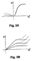
- FIGS. 3A and 3B illustrate characteristics of a TFT.
- FIG. 4 is a plan view schematically showing an EL display device of the present invention.
- FIGS. 5A and 5B are cross sectional views taken along the lines A—A and B—B in FIG. 4, respectively.
- FIG. 6 illustrates timing charts for driving the EL display device of the present invention.
- FIG. 7 is a cross sectional view of an EL display device of the present invention with a different structure, taken along the line A—A in FIG. 4 .
- FIGS. 8A and 8B are cross sectional views of an EL display device of the present invention with different structures, taken along the lines A—A and B—B in FIG. 4, respectively.
- FIG. 4 is a plan view showing a single display pixel when the present invention is applied to an organic EL display device.
- FIGS. 5A and 5B are cross sectional views taken along the lines A—A and B—B in FIG. 4, respectively.
- a display pixel is formed in a region surrounded by gate signal lines 51 and drain signal lines 52 .
- a first TFT 30 is provided adjacent to an intersection of these lines.
- the TFT 30 has a source 13 s serving as an electrode 55 forming a storage capacitor with a storage capacitor electrode line 54 described hereinafter, and connected to a gate 41 of a second TFT 40 .
- the second TFT 40 has a source 43 s connected to an anode 61 of an organic EL element, and a drain 43 d connected to a driving power supply line 53 for driving the organic EL element.
- the storage capacitor electrode line 54 is disposed in parallel to the gate signal line 51 near the TFT.
- This line 54 may be formed of chromium or the like, and electric charges are stored between the line 54 and the capacitor electrode 55 connected to the source 13 s of the TFT with a gate insulating film 12 interposed therebetween.
- the storage capacitor electrode line 54 and the capacitor electrode 55 form a storage capacitor, which is provided for retaining the voltage applied to the gate electrode 41 of the second TFT 40 .
- the organic EL display device is formed by stacking TFTs and organic EL elements in order on a substrate 10 such as a substrate formed of glass, synthetic resin, or the like, a conductive substrate, and a semiconductor substrate. It should be noted that when a conductive or semiconductor substrate is used for the substrate 10 , the TFTs and organic EL display device are provided on an insulating film of SiO 2 , SiN, or the like, which is formed on the substrate 10 .
- both the first and second TFTS and 40 are of the bottom gate type, in which a gate electrode is provided under an active layer 13 formed of polycrystalline silicon (hereinafter referred to as “p-Si”) film.
- the TFT in this embodiment also includes the gate electrode 11 of the double gate type.
- the first TFT 30 for switching operation will next be described.
- the gate signal line 51 which also serves as the gate electrode 11 and formed of refractory metal such as chromium (Cr) and molybdenum (Mo), and the drain signal line 52 formed of Al are provided on the insulating substrate 10 formed of, for example, quartz glass, non-alkaline glass, or the like.
- the driving power supply line 53 is formed of Al, serving as a driving power supply for the organic EL element and connected to the driving power supply.
- a gate insulating film 12 , and the active layer 13 of a p-Si film are formed in this order.
- the active layer 13 is of a so-called LDD (lightly doped drain) structure. More specifically, ions are doped using a stopper insulating film 14 located on a channel 13 c over the gate electrode 11 as a mask. Ions are further doped using a resist which covers the gate electrode 11 and the regions located on both sides of the gate electrode 11 within a predetermined distance, to thereby form a lightly doped region 13 LD (indicated as the shaded area in the figure with the lines slanting from the upper left to the lower right) on either side of the gate electrode 11 , and the source 13 s and a drain 13 d as highly doped regions (indicated as the shaded areas in the figure with the line slanting from the upper right to the lower left) located outside the lightly doped regions.
- LDD lightly doped drain
- An interlayer insulating film 15 formed of an SiO 2 film, an SiN film and an SiO 2 film in that order, is provided on the entire surface, covering the gate insulating film 12 , the active layer 13 , and the stopper insulating film 14 .
- a drain electrode 16 is formed by filling metal such as Al in a contact hole provided corresponding to the drain 13 d .
- a planarization insulating film 17 is formed of organic resin or the like on the entire surface for planarization.
- the second TFT 40 for driving the organic EL element will next be described.
- the gate electrode 41 is formed of refractory metal such as Cr and Ho on the insulating substrate formed of silica glass, non-alkaline glass, or the like.
- the gate insulating film 12 and an active layer 43 formed of a p-Si film are formed in succession.
- the active layer 43 includes an intrinsic, or substantially intrinsic, channel 43 c provided over the gate electrode 41 , and the source 43 s and the drain 43 d provided on respective sides of the channel 43 c by doping ions using a resist to cover these side regions.
- the interlayer insulating film 15 is next formed of an SiO 2 film, an SiN film and an SiO 2 film in this order over the entire surface to cover the gate insulating film 12 and the active layer 43 .
- the driving power supply line 53 connected to a driving power supply 50 is formed by filling a metal such as Al in a contact hole provided corresponding to the drain 43 d .
- the planarization insulating film 17 of organic resin or the like is formed over the entire surface for the purpose of planarization.
- a contact hole CH is formed in the planarization insulating film 17 at a position corresponding to the source 43 s .
- a transparent electrode formed of ITO, i.e. the anode 61 of the organic EL element, is formed on the planarization insulating film 17 so as to connect to the source 43 s through the contact hole CH.
- the organic EL element 60 has a general structure, provided by stacking the anode 61 formed of a transparent electrode of ITO (indium tin oxide) or the like, a first hole-transport layer 62 of MTDATA (4,4-bis(3-methylphenylphenylamino)biphenyl), a second hole-transport layer 63 of TPD (4,4,4-tris(3-methylphenylphenylamino)triphenylamine), a light emissive layer 64 of Bebq2(10-benzo(h)quinolinol-beryllium complex) including quinacridon derivatives, a light emissive element layer 65 formed of an electron-transport layer of Bebq2, and a cathode 66 of magnesium-indium alloy, in this order.
- ITO indium tin oxide
- MTDATA bis(3-methylphenylphenylamino)biphenyl
- TPD 4,4,4-tris(3-methylphenylphen
- holes and electrons injected from the anode and cathode, respectively, are recombined in the light emissive layer to excite organic molecules forming the light missive layer, thereby producing exactions.
- Light is released from the light emissive layer during the process in which the exactions deactivate, and this release of light to the outside from the transparent anode through the transparent insulating substrate results in light being emitted.
- FIG. 6 illustrates signal timing charts. It should be noted that the circuit of the organic EL display device according to the present embodiment corresponds to that shown in FIG. 1 .
- the charts (a)-(c) show timings of the signal VG(n) 1 supplied to the gate electrode of the first TFT in the n th row, the drain signal VD in the m th column, and the signal VG(n) 2 at the gate electrode of the second TFT in the n th row, respectively.
- the first TFT attains and maintains the ON state for a horizontal period (1H), after which it is switched off.
- the drain signal shown in FIG. 6 ( b ) is applied from the drain signal line Dm to the gate electrode 41 through the source 43 s , whereby the gate electrode 41 attains the same potential as the drain signal line Dm.
- the second TFT 40 is turned on, and a current of the value corresponding to that of the gate electrode 41 is supplied from the driving power supply 50 to the anode 61 of the organic EL element 60 through the drain 43 d and the source 43 s .
- the organic EL element 60 emits light.
- the display pixels having the above-described structure are arranged in a matrix on the substrate 10 to form an organic EL display device.
- the first TFT 30 is an n-channel TFT with an LDD structure, having the active layer 13 with the source and drain doped with n-type impurities, so that a high electric-field mobility can be achieved, and a leakage current of the first TFT 30 can be suppressed. Therefore, writing operation can be performed at a high speed, and a good voltage retaining properties can be obtained. Consequently, writing can be achieved following the drain signal that changes each horizontal period ( 1 H) as shown in FIG. 6 ( b ), and the potential of the gate electrode 41 can be maintained as indicated by the solid line in FIG. 6 ( c ) without a change observed in devices of the related art as indicated by the broken line in the figure.
- a high ON current can be achieved as indicated by the solid line in FIG. 3A, making it possible to supply the current for light emission to the organic EL element in a stable manner without a decrease.
- the second TFT 40 is a p-channel TFT having an active layer with the source and drain doped with p-type impurities, a wider saturation region of the Id-vd characteristics can be achieved as indicated by the solid line in FIG. 3B, so that the value Id is not easily changed in accordance with the value Vd.
- variation in the value of the drain current caused by the change in the drain voltage can be reduced, whereby the emitted luminance of the organic EL device can be made uniform with good reproductivity, so that a quality gradation display gray scale) can be obtained.
- grain boundaries are present especially in the polycrystalline silicon TFT, resulting in a potential barrier to be created by electrons trapped in the grain boundaries, and in spread of a depletion layer. Consequently, a strong electric field is applied to the grain boundaries at the edges of the drain electrode, generating a collisional ionization phenomenon where the accelerated electrons collide with lattices. This phenomenon is much more insignificant in a p-channel TFT than in an n-channel TFT, and the drain current exhibits a saturation region to provide good saturation characteristics. Therefore, a p-channel TFT is used for the second TFT.
- the first TFT with an n-channel and the LDD structure, and the second TFT with a p-channel are employed, to thereby provide an organic EL display device which allows a high-speed writing and reduction in leakage current and provides emitted luminance with good reproductivity.
- FIG. 7 is a cross sectional view illustrating the first TFT of the EL display device according to the present invention.
- the device of the second embodiment differs from that of the first embodiment primarily in that the first TFT has an n-channel, and a double gate structure and an offset structure as shown in FIG. 7 .
- an active layer of p-Si provided on the stacked layers of the gate electrode 11 and the gate insulating film 12 includes intrinsic or substantially intrinsic regions 130 S over the gate electrode 11 on both sides thereof. These regions function as so-called offset regions the TFT further includes the source 13 s and the drain 13 d doped with n-type impurities such as phosphorus indicated by the shaded regions in FIG. 7 . Thus, the first TFT has a so-called offset structure including such offset regions.
- the first n-channel TFT has double gate and offset structures, both high electric-field mobility and a reduction in a leakage current are obtained. Further, by using a p-channel TFT as the second TFT as in the first embodiment, variation in the drain current caused by the drain voltage can be reduced, providing an organic EL display device having organic EL elements with uniform emitted luminance and good reproductivity and allowing a good gradation display.
- the present embodiment relates to a device which includes TFTs of the so-called top gate type, where the gate electrode is provided over the active layer 13 , as the first and second TFTs 30 and 40 .
- the TFT in this embodiment includes the gate electrodes 11 to form a double gate structure.
- FIGS. 8A and 8B are cross sectional views respectively illustrating the first and second TFTs.
- an active layer of p-Si is formed on the insulating substrate 10 .
- the active layer 13 includes channels 13 c overlapping the two gate electrodes 11 with the gate insulating film 12 interposed therebetween, and lightly doped regions 13 LD doped with n-type, low concentration impurities such as phosphorus and provided on both sides of the channels 13 c .
- heavily doped regions doped with n-type impurities are formed as the source 13 s and the drain 13 d.
- the first switching TFT having the LDD structure and the top gate structure are formed.
- the active layer 43 is formed on the insulating substrate 10 at the same time the active layer 13 of the first TFT is formed.
- the active layer 43 includes the channel 43 c overlapping the two gate electrodes 41 with the gate insulating film 12 interposed therebetween, and the source 43 s and the drain 43 d formed on both sides of the channel 43 c by doping p-type impurities such as boron (B).
- the source 43 s is connected to the anode 61 of the organic EL element.
- the structure of the organic EL element will not be described again because the structure corresponds to that structure previously described with reference to the first embodiment.
- the second p-channel TFT used for driving the organic EL element is thus formed.
- first and second TFTs with top gate structures also exhibit a high electric-field mobility, leading to a high-speed writing and a smaller leakage current, to thereby obtain the first TFT with good voltage-retaining properties, and the second TFT with superior saturation characteristics and less variation in current.
- an organic EL display device that excels in video signal retaining properties and provides a good gradation display can be achieved.
- the present invention is not limited thereto, and can be applied to a multigate structure having three or more gate electrodes.
- a p-Si film is used for the active layer in the above embodiments, a microcrystalline silicon film or an amorphous silicon film can also be used.
- an organic EL display device is described in the above embodiments, the present invention is not limited to application thereto, and can also be applied, with similar effect, to other light emissive display devices such as an inorganic El display device having a light emissive layer of inorganic material or to a vacuum fluorescent display having a fluorescent layer between an anode and a cathode.
Abstract
An organic EL display device including a first TFT (30) for switching operation, a second TFT (40) for driving an organic EL element, and an organic EL element (60) having an anode (61), a cathode (66), and a light emissive element layer (65) sandwiched between these electrodes. The first TFT (30) has an n-channel and an LDD structure, exhibiting a high-speed response and superior retaining characteristics. The second TFT (40) has a p-channel, and therefore exhibits superior current controllability. By combining these two types of TFTs to drive the organic EL element for each pixel, a high ON current can be achieved with a reduced leakage current, thereby producing a quality gradation display.
Description
1. Field of the Invention
The present invention relates to an electroluminescence display device provided with an electroluminescence element and a thin film transistor.
2. Description of the Related Art
In recent years, electroluminescence (hereinafter referred to as EL) display devices employing EL elements have attracted attention as an alternatives to devices such as CRTs and LCDs. For example, EL display devices including a thin film transistor (hereinafter referred to as TFT) used as a switching element for driving the EL elements have been researched and developed.
FIG. 1 is an equivalent circuit diagram of a related art EL display device including an EL element and TFTS.
The EL display device shown in FIG. 1, which illustrates a portion near a gate signal line Gn in the nth row and a drain signal line Dm in the mth column, includes first and second TFTS 130 and 140, and an organic EL element 160.
The gate signal line Gn for supplying a gate signal and a drain signal line Dm for supplying a drain signal cross each other, and the organic EL element 160 and the TFTs 130 and 140 for driving the organic EL element 160 are provided near an intersection of these signal lines.
The first TFT 130 for switching operation includes a gate electrode 131 connected to the gate signal line Gn and receiving the gate signal, a drain electrode 132 connected to the drain signal line Dm and receiving the drain signal, and a source electrode 133 connected to a gate electrode 141 of the second TFT 140.
The second TFT 140 for driving the organic EL element includes the gate electrode 141 connected to the source electrode 133 of the first TFT 130, a source electrode 142 connected to an anode 161 of the organic EL element 160, and a drain electrode 143 connected to a driving power supply 150 for supplying a current to the organic EL element 160.
The organic EL element 160 includes the anode 161 connected to the source electrode 142, a cathode 162 connected to a common electrode 164, and a light emissive element layer 163 sandwiched between the anode 161 and the cathode 162.
The device further includes a storage capacitor 170 having one electrode 171 connected between the source electrode 133 of the first TFT 130 and the gate electrode 141 of the second TFT 140, and the other electrode 172 connected to a common electrode 173.
A method of driving the circuit shown in the equivalent circuit diagram of FIG. 1 will next be described with reference to signal timing charts in FIG. 2, in which signal timings of a signal VG(n)1 supplied to the gate electrode 131 of the first TFT 130 in the nth row, a drain signal VD at the drain signal line Dm, and a signal VG(n)2 supplied to the gate electrode 141 of the second TFT 140 in the nth row are illustrated in (a)-(c), respectively.
When the gate signal VG(n)1 illustrated in FIG. 2(a) is applied from the gate signal line Gn to the gate electrode 131, the first TFT 130 is switched on. As a result, the drain signal VD illustrated in FIG. 2(b) is supplied from the drain signal line Dm to the gate electrode 141, which attains the same potential as the drain signal line Dm. A current corresponding to the value of a voltage applied to the gate electrode 141 is then supplied from the driving power supply 150 to the EL element 160, which is caused to emit light.
It should be noted that in actual operation, while the first TFT 130 is in ON state, a current flows until the gate electrode 141 attains the same potential as the drain signal line Dm and electric charges are stored in a gate capacitor of the gate electrode 141. After the first TFT 130 is turned off,the electric charges stored in the gate capacitor must be maintained, and also the potential of the gate must be retained as illustrated by the broken line in FIG. 2(c).
In the above-described EL display device, however, a leakage current flows during the OFF period of the TFT. As a result, when the drain signal VD changes every horizontal period (IH) as illustrated in FIG. 2(b), the potential VG(n)2 of the gate electrode 141 cannot be maintained, but is changed as shown by the solid line in FIG. 2(c).
More specifically, as illustrated by the solid line in FIG. 2(c), (i) when the potential of the drain signal line Dm is lower than that supplied to the gate electrode 141, a leakage current flows to the drain signal line Di through the first TFT 130, decreasing the potential of the gate electrode 141; and (ii) when the potential of the drain signal line Dm is higher than that supplied to the gate electrode 141, a leakage current flows to the gate electrode 141 through the first TFT 130, resulting in further storage of electric charges in the gate capacitor and in a higher potential of the gate electrode 141.
In configuration (i) above, the organic EL element 160 receives a current larger than it is supposed to receive, leading to a higher luminance of the organic EL element. On the other hand, the element 160 will have a lower luminance in configuration (ii) above.
With either configuration, the device has a drawback in that it is difficult to cause each display pixel to emit light at the appropriate luminance when a large leakage current flows through the first TFT 130 as indicated by the solid line in FIG. 2(c).
The second TFT serves to control the current supplied from the power supply for driving the organic EL element in accordance with the voltage applied to the gate of the second TFT, and supply it to the organic EL element. The second TFT has an active layer that includes an intrinsic or substantially intrinsic channel region overlapping its gate, and source and drain regions located on both sides of the channel region and having impurities doped therein.
However, when the second TFT is an n-channel transistor, a so-called saturation region of the drain current-drain voltage (Id-vd) characteristics, i.e. a region where the drain current Id is constant even though the drain voltage vd is increased, is extremely narrow (saturation characteristics are poor), as indicated by broken lines in FIG. 3B. Consequently, the current value Id is increased with an increase in the value of Vd, and therefore a constant current cannot be obtained, but is affected by the voltage Vd, leading to a poor current controllability.
Especially when the TFT is formed of polycrystalline silicon, there exist grain boundaries of crystals, and electrons are trapped therein to form a potential barrier, thereby spreading a depletion layer. As a result, a strong electric field is applied to the grain boundaries at the edges of the drain electrode, whereby a collisional ionization phenomenon, in which accelerated electrons collide with lattices, occurs and the drain current is not saturated, but increased. This is a significant problem in the n-channel TFT, but rare in the p-channel TFT.
The present invention has been conceived in view of the above-described problems, and an object thereof is to provide an EL display device which creates a superior gradation (gray scale) display by, expressed in the terminology introduced above, suppressing a leakage current at the first TFT 130 to maintain the potential at the gate electrode 141 of the second TFT 140, and improving current controllability of the second TFT 140.
According to one aspect, the present invention provides an electroluminescence device which includes an electroluminescence element having a light emissive layer provided between first and second electrodes, a first thin film transistor receiving a selection signal at its gate to acquire a data signal, and a second thin film transistor provided between a driving power supply and the electroluminescence element and controlling power supplied from the driving power supply to the electroluminescence element in accordance with the data signal applied from the first thin film transistor. In this electroluminescence device, the first thin film transistor has an n-channel, and at least one of a lightly doped drain structure, an offset structure, and a multigate structure, and the second thin film transistor has a p-channel.
By employing an n-channel transistor as the first thin film transistor in this manner, a quick response can be achieved at the transistor. Further, by employing at least one of the lightly doped drain structure, the offset structure, and the multigate structure in the first thin film transistor, an off-leakage current at the transistor can be reduced, and a quick response can be made in accordance with the selection signal applied to the gate to acquire and surely maintain the data signal. When a p-channel transistor is used for the second thin film transistor, a stable current can be output in response to the drain voltage, making it possible to supply power (or current when an organic EL element is used) to the electroluminescence element from the driving power supply in a stable manner, and to suppress variation in emitted luminance at the element.
According to another aspect of the present invention, the first and second thin film transistors of the electroluminescence device include an active layer formed of non-single crystalline semiconductor layer.
According to a still another aspect of the present invention, the non-single crystalline semiconductor layer is a polycrystalline silicon layer.
According to a further aspect of the present invention, the first and second thin film transistors are of top gate or bottom gate type, having a gate electrode above or below their active layer.
According to a further aspect of the present invention, the electroluminescence element and the first and second thin film transistors form a pixel of the device, and a plurality of such pixels are arranged in a matrix on a substrate.
According to a further aspect of the present invention, drains of the respective first thin film transistors for the pixels assigned to the same column among the plurality of pixels arranged in the matrix are connected to the same data line, while gates of the respective first thin film transistors for the pixels assigned to the same row among the plurality of pixels arranged in the matrix are connected to the same scan line.
According to a further aspect of the present invention, the electroluminescence device further includes a storage capacitor connected between a source of the first thin film transistor and a gate of the second thin film transistor, and the non-single crystalline semiconductor layer used for the active layer of the first thin film transistor also serves as one electrode of the storage capacitor.
By thus providing a storage capacitor for each pixel, the data signal acquired while the first thin film transistor is selected and thus in the ON state can be maintained until the first thin film transistor is next selected, contributing to improvement in display quality. In addition, by thus forming one electrode of the storage capacitor by the non-single crystalline semiconductor film used as the active layer of the transistor, increase in number of manufacturing steps for forming the electrodes of the storage capacitor can be minimized.
According to a further aspect of the present invention, the electroluminescence element is an organic electroluminescence element having a light emissive layer formed of an organic compound. In a color display device or the like, it can be extremely advantageous to have such a light emissive layer formed of an organic compound because this configuration provides a wide variety of displayable colors and a wide range of options for the material used.
According to a further aspect, the present invention provides an electroluminescence display device which includes an electroluminescence element having a light emissive layer provided between an anode and a cathode; a first thin film transistor having an active layer which is formed of a non-single crystalline semiconductor film and which includes a source connected to a storage capacitor, a drain connected to a drain signal line, and a gate electrode provided over a channel of the active layer and connected to a gate signal line; and a second thin film transistor having an active layer which is formed of a non-single crystalline semiconductor film and which includes a drain connected to a driving power supply of the electroluminescence element, and a gate electrode connected to the source of the first thin film transistor. In the above electroluminescence display device, the first thin film transistor has an n-channel and at least one of a lightly doped drain structure, an offset structure, and a multigate structure, while the second thin film transistor has a p-channel.
In a further aspect, the present invention provides an electroluminescence display device which includes an electroluminescence element having a light emissive layer provided between an anode and a cathode; a first thin film transistor having an active layer which is formed of a non-single crystalline semiconductor film and which includes a source connected to a storage capacitor, a drain connected to a drain signal line, and a gate electrode provided under a channel of the active layer and connected to a gate signal line; and a second thin film transistor having an active layer which is formed of a non-single crystalline semiconductor film and which includes a drain connected to a driving power supply of the electroluminescence element, and a gate electrode connected to the source of the first thin film transistor. In the above electroluminescence display device, the first thin film transistor has an n-channel and at least one of a lightly doped drain structure, an offset structure, and a multigate structure, while the second thin film transistor has a p-channel.
Because the above-described EL device and EL display device according to the present invention includes the first TFT allowing high speed writing with good retention characteristics and the second TFT with good current controllability, an excellent gradation (gray scale) display can be realized.
FIG. 1 is an equivalent circuit diagram of an organic EL display device of a related art.
FIG. 2 illustrates timing charts for driving an organic EL display device of the related art.
FIGS. 3A and 3B illustrate characteristics of a TFT.
FIG. 4 is a plan view schematically showing an EL display device of the present invention.
FIGS. 5A and 5B are cross sectional views taken along the lines A—A and B—B in FIG. 4, respectively.
FIG. 6 illustrates timing charts for driving the EL display device of the present invention.
FIG. 7 is a cross sectional view of an EL display device of the present invention with a different structure, taken along the line A—A in FIG. 4.
FIGS. 8A and 8B are cross sectional views of an EL display device of the present invention with different structures, taken along the lines A—A and B—B in FIG. 4, respectively.
Preferred embodiments of EL display devices of the present invention will next be described.
FIG. 4 is a plan view showing a single display pixel when the present invention is applied to an organic EL display device.
FIGS. 5A and 5B are cross sectional views taken along the lines A—A and B—B in FIG. 4, respectively.
Referring to FIG. 4, a display pixel is formed in a region surrounded by gate signal lines 51 and drain signal lines 52.
A first TFT 30 is provided adjacent to an intersection of these lines. The TFT 30 has a source 13 s serving as an electrode 55 forming a storage capacitor with a storage capacitor electrode line 54 described hereinafter, and connected to a gate 41 of a second TFT 40. The second TFT 40 has a source 43 s connected to an anode 61 of an organic EL element, and a drain 43 d connected to a driving power supply line 53 for driving the organic EL element.
The storage capacitor electrode line 54 is disposed in parallel to the gate signal line 51 near the TFT. This line 54 may be formed of chromium or the like, and electric charges are stored between the line 54 and the capacitor electrode 55 connected to the source 13 s of the TFT with a gate insulating film 12 interposed therebetween. The storage capacitor electrode line 54 and the capacitor electrode 55 form a storage capacitor, which is provided for retaining the voltage applied to the gate electrode 41 of the second TFT 40.
Referring to FIGS. 5A and 5B, the organic EL display device is formed by stacking TFTs and organic EL elements in order on a substrate 10 such as a substrate formed of glass, synthetic resin, or the like, a conductive substrate, and a semiconductor substrate. It should be noted that when a conductive or semiconductor substrate is used for the substrate 10, the TFTs and organic EL display device are provided on an insulating film of SiO2, SiN, or the like, which is formed on the substrate 10.
In the present embodiment, both the first and second TFTS and 40 are of the bottom gate type, in which a gate electrode is provided under an active layer 13 formed of polycrystalline silicon (hereinafter referred to as “p-Si”) film. The TFT in this embodiment also includes the gate electrode 11 of the double gate type.
The first TFT 30 for switching operation will next be described.
Referring again to FIG. 5A, the gate signal line 51 which also serves as the gate electrode 11 and formed of refractory metal such as chromium (Cr) and molybdenum (Mo), and the drain signal line 52 formed of Al are provided on the insulating substrate 10 formed of, for example, quartz glass, non-alkaline glass, or the like. Next, the driving power supply line 53 is formed of Al, serving as a driving power supply for the organic EL element and connected to the driving power supply.
Thereafter, a gate insulating film 12, and the active layer 13 of a p-Si film are formed in this order.
The active layer 13 is of a so-called LDD (lightly doped drain) structure. More specifically, ions are doped using a stopper insulating film 14 located on a channel 13 c over the gate electrode 11 as a mask. Ions are further doped using a resist which covers the gate electrode 11 and the regions located on both sides of the gate electrode 11 within a predetermined distance, to thereby form a lightly doped region 13LD (indicated as the shaded area in the figure with the lines slanting from the upper left to the lower right) on either side of the gate electrode 11, and the source 13 s and a drain 13 d as highly doped regions (indicated as the shaded areas in the figure with the line slanting from the upper right to the lower left) located outside the lightly doped regions.
An interlayer insulating film 15, formed of an SiO2 film, an SiN film and an SiO2 film in that order, is provided on the entire surface, covering the gate insulating film 12, the active layer 13, and the stopper insulating film 14. A drain electrode 16 is formed by filling metal such as Al in a contact hole provided corresponding to the drain 13 d. Further, a planarization insulating film 17 is formed of organic resin or the like on the entire surface for planarization.
The second TFT 40 for driving the organic EL element will next be described.
Referring to FIG. 5B, the gate electrode 41 is formed of refractory metal such as Cr and Ho on the insulating substrate formed of silica glass, non-alkaline glass, or the like.
The gate insulating film 12 and an active layer 43 formed of a p-Si film are formed in succession.
The active layer 43 includes an intrinsic, or substantially intrinsic, channel 43 c provided over the gate electrode 41, and the source 43 s and the drain 43 d provided on respective sides of the channel 43 c by doping ions using a resist to cover these side regions.
The interlayer insulating film 15 is next formed of an SiO2 film, an SiN film and an SiO2 film in this order over the entire surface to cover the gate insulating film 12 and the active layer 43. The driving power supply line 53 connected to a driving power supply 50 is formed by filling a metal such as Al in a contact hole provided corresponding to the drain 43 d. The planarization insulating film 17 of organic resin or the like is formed over the entire surface for the purpose of planarization. A contact hole CH is formed in the planarization insulating film 17 at a position corresponding to the source 43 s. A transparent electrode formed of ITO, i.e. the anode 61 of the organic EL element, is formed on the planarization insulating film 17 so as to connect to the source 43 s through the contact hole CH.
The organic EL element 60 has a general structure, provided by stacking the anode 61 formed of a transparent electrode of ITO (indium tin oxide) or the like, a first hole-transport layer 62 of MTDATA (4,4-bis(3-methylphenylphenylamino)biphenyl), a second hole-transport layer 63 of TPD (4,4,4-tris(3-methylphenylphenylamino)triphenylamine), a light emissive layer 64 of Bebq2(10-benzo(h)quinolinol-beryllium complex) including quinacridon derivatives, a light emissive element layer 65 formed of an electron-transport layer of Bebq2, and a cathode 66 of magnesium-indium alloy, in this order.
In the organic EL element, holes and electrons injected from the anode and cathode, respectively, are recombined in the light emissive layer to excite organic molecules forming the light missive layer, thereby producing exactions. Light is released from the light emissive layer during the process in which the exactions deactivate, and this release of light to the outside from the transparent anode through the transparent insulating substrate results in light being emitted.
FIG. 6 illustrates signal timing charts. It should be noted that the circuit of the organic EL display device according to the present embodiment corresponds to that shown in FIG. 1.
Referring to FIG. 6, the charts (a)-(c) show timings of the signal VG(n)1 supplied to the gate electrode of the first TFT in the nth row, the drain signal VD in the mth column, and the signal VG(n)2 at the gate electrode of the second TFT in the nth row, respectively.
As shown in FIG. 6(a), when the gate signal is applied to the gate 11 connected to the gate signal line Gn, the first TFT attains and maintains the ON state for a horizontal period (1H), after which it is switched off. Referring to FIG. 6(c), when the first TFT attains the ON state, the drain signal shown in FIG. 6(b) is applied from the drain signal line Dm to the gate electrode 41 through the source 43 s, whereby the gate electrode 41 attains the same potential as the drain signal line Dm. When the gate electrode 41 attains this potential, the second TFT 40 is turned on, and a current of the value corresponding to that of the gate electrode 41 is supplied from the driving power supply 50 to the anode 61 of the organic EL element 60 through the drain 43 d and the source 43 s. As a result, the organic EL element 60 emits light.
The display pixels having the above-described structure are arranged in a matrix on the substrate 10 to form an organic EL display device.
As described above, according to the present invention, the first TFT 30 is an n-channel TFT with an LDD structure, having the active layer 13 with the source and drain doped with n-type impurities, so that a high electric-field mobility can be achieved, and a leakage current of the first TFT 30 can be suppressed. Therefore, writing operation can be performed at a high speed, and a good voltage retaining properties can be obtained. Consequently, writing can be achieved following the drain signal that changes each horizontal period (1H) as shown in FIG. 6(b), and the potential of the gate electrode 41 can be maintained as indicated by the solid line in FIG. 6(c) without a change observed in devices of the related art as indicated by the broken line in the figure. In addition, a high ON current can be achieved as indicated by the solid line in FIG. 3A, making it possible to supply the current for light emission to the organic EL element in a stable manner without a decrease.
As the second TFT 40 is a p-channel TFT having an active layer with the source and drain doped with p-type impurities, a wider saturation region of the Id-vd characteristics can be achieved as indicated by the solid line in FIG. 3B, so that the value Id is not easily changed in accordance with the value Vd. In other words, variation in the value of the drain current caused by the change in the drain voltage can be reduced, whereby the emitted luminance of the organic EL device can be made uniform with good reproductivity, so that a quality gradation display gray scale) can be obtained.
As described earlier in the specification, grain boundaries are present especially in the polycrystalline silicon TFT, resulting in a potential barrier to be created by electrons trapped in the grain boundaries, and in spread of a depletion layer. Consequently, a strong electric field is applied to the grain boundaries at the edges of the drain electrode, generating a collisional ionization phenomenon where the accelerated electrons collide with lattices. This phenomenon is much more insignificant in a p-channel TFT than in an n-channel TFT, and the drain current exhibits a saturation region to provide good saturation characteristics. Therefore, a p-channel TFT is used for the second TFT.
As described above, the first TFT with an n-channel and the LDD structure, and the second TFT with a p-channel are employed, to thereby provide an organic EL display device which allows a high-speed writing and reduction in leakage current and provides emitted luminance with good reproductivity.
FIG. 7 is a cross sectional view illustrating the first TFT of the EL display device according to the present invention.
The device of the second embodiment differs from that of the first embodiment primarily in that the first TFT has an n-channel, and a double gate structure and an offset structure as shown in FIG. 7.
Referring to FIG. 7, in the first TFT, an active layer of p-Si provided on the stacked layers of the gate electrode 11 and the gate insulating film 12 includes intrinsic or substantially intrinsic regions 130S over the gate electrode 11 on both sides thereof. These regions function as so-called offset regions the TFT further includes the source 13 s and the drain 13 d doped with n-type impurities such as phosphorus indicated by the shaded regions in FIG. 7. Thus, the first TFT has a so-called offset structure including such offset regions.
Because the first n-channel TFT has double gate and offset structures, both high electric-field mobility and a reduction in a leakage current are obtained. Further, by using a p-channel TFT as the second TFT as in the first embodiment, variation in the drain current caused by the drain voltage can be reduced, providing an organic EL display device having organic EL elements with uniform emitted luminance and good reproductivity and allowing a good gradation display.
The present embodiment relates to a device which includes TFTs of the so-called top gate type, where the gate electrode is provided over the active layer 13, as the first and second TFTs 30 and 40. In addition, the TFT in this embodiment includes the gate electrodes 11 to form a double gate structure.
FIGS. 8A and 8B are cross sectional views respectively illustrating the first and second TFTs.
Referring to FIG. 8A, an active layer of p-Si is formed on the insulating substrate 10. The active layer 13 includes channels 13 c overlapping the two gate electrodes 11 with the gate insulating film 12 interposed therebetween, and lightly doped regions 13LD doped with n-type, low concentration impurities such as phosphorus and provided on both sides of the channels 13 c.
Further, heavily doped regions doped with n-type impurities are formed as the source 13 s and the drain 13 d.
Thus, the first switching TFT having the LDD structure and the top gate structure are formed.
Referring to FIG. 8B, the active layer 43 is formed on the insulating substrate 10 at the same time the active layer 13 of the first TFT is formed. Similarly to the first TFT, the active layer 43 includes the channel 43 c overlapping the two gate electrodes 41 with the gate insulating film 12 interposed therebetween, and the source 43 s and the drain 43 d formed on both sides of the channel 43 c by doping p-type impurities such as boron (B). The source 43 s is connected to the anode 61 of the organic EL element. The structure of the organic EL element will not be described again because the structure corresponds to that structure previously described with reference to the first embodiment.
The second p-channel TFT used for driving the organic EL element is thus formed.
As described above, similarly to those with a bottom gate structure, first and second TFTs with top gate structures also exhibit a high electric-field mobility, leading to a high-speed writing and a smaller leakage current, to thereby obtain the first TFT with good voltage-retaining properties, and the second TFT with superior saturation characteristics and less variation in current.
As a result, an organic EL display device that excels in video signal retaining properties and provides a good gradation display can be achieved.
While the first TFT is described as having a double gate structure in the above embodiments, the present invention is not limited thereto, and can be applied to a multigate structure having three or more gate electrodes.
Likewise, although a p-Si film is used for the active layer in the above embodiments, a microcrystalline silicon film or an amorphous silicon film can also be used.
While an organic EL display device is described in the above embodiments, the present invention is not limited to application thereto, and can also be applied, with similar effect, to other light emissive display devices such as an inorganic El display device having a light emissive layer of inorganic material or to a vacuum fluorescent display having a fluorescent layer between an anode and a cathode.
Claims (11)
1. An electroluminescence device, comprising:
an electroluminescence element having a light emissive layer provided between first and second electrodes;
a first thin film transistor receiving a selection signal at its gate to acquire a data signal; and
a second thin film transistor provided between a driving power supply and said electroluminescence element, and controlling power supplied from said driving power supply to said electroluminescence element in accordance with the data signal supplied from said first thin film transistor; wherein
said first thin film transistor is a double gate type having a lightly doped drain structure, said first thin film transistor has at least one of an n-channel, an offset structure, and a multigate structure; and
said second thin film transistor has a p-channel.
2. The electroluminescence device according to claim 1 , wherein said first and second thin film transistors include an active layer formed of non-single crystalline semiconductor layer.
3. The electroluminescence device according to claim 2 , wherein said non-single crystalline semiconductor layer is a polycrystalline silicon layer.
4. The electroluminescence device according to claim 1 , wherein said first and second thin film transistors are of top gate or bottom gate type, having a gate electrode above or below their active layer.
5. The electroluminescence device according to claim 1 , wherein said electroluminescence element and said first and second thin film transistors form a pixel of the device, and a plurality of said pixels are arranged in a matrix on a substrate.
6. The electroluminescence device according to claim 5 , wherein
drains of the respective first thin film transistors for pixels assigned to a same column among said plurality of pixels arranged in the matrix are connected to the same data line, and
gates of the respective first thin film transistors for pixels assigned to a same row among said plurality of pixels arranged in the matrix are connected to the same scan line.
7. The electroluminescence device according to claim 6 , further comprising a storage capacitor connected between a source of said first thin film transistor and a gate of said second thin film transistor, wherein
a non-single crystalline semiconductor layer used for the active layer of said first thin film transistor also serves as one electrode of the storage capacitor.
8. The electroluminescence device according to claim 1 , wherein said electroluminescence element is an organic electroluminescence element having a light emissive layer formed of an organic compound.
9. An electroluminescence display device, comprising:
an electroluminescence element having a light emissive layer provided between an anode and a cathode;
a first thin film transistor having an active layer which is formed of a non-single crystalline semiconductor film and which includes a source connected to a storage capacitor, a drain connected to a drain signal line, and a gate electrode provided over a channel of said active layer and connected to a gate signal line; and
a second thin film transistor having an active layer which is formed of a non-single crystalline semiconductor film and which includes a drain connected to a driving power supply of said electroluminescence element, and a gate electrode connected to the source of said first thin film transistor; wherein
said first thin film transistor is a double gate type having a lightly doped drain structure, said first thin film transistor has at least one of an n-channel, an offset structure, and a multigate structure; and
said second thin film transistor has a p-channel.
10. An electroluminescence display device, comprising:
an electroluminescence element having a light emissive layer provided between an anode and a cathode;
a first thin film transistor having an active layer which is formed of a non-single crystalline semiconductor film and which includes a source connected to a storage capacitor, a drain connected to a drain signal line, and a gate electrode provided under a channel of said active layer and connected to a gate signal line; and
a second thin film transistor having an active layer which is formed of a non-single crystalline semiconductor film and which includes a drain connected to a driving power supply of said electroluminescence element, and a gate electrode connected to the source of said first thin film transistor; wherein
said first thin film transistor is a double gate type having a lightly doped drain structure, said first thin film transistor has at least one of an n-channel, an offset structure, and a multigate structure; and
said second thin film transistor has a p-channel.
11. A light emissive device, comprising:
a light emissive element having a light emissive layer provided between first and second electrodes;
a first thin film transistor receiving a selection signal at its gate to acquire a data signal; and
a second thin film transistor provided between a driving power supply and said element, and controlling power supplied from said driving power supply to said element in accordance with the data signal supplied from said first thin film transistor, wherein
said first thin film transistor is a double gate type having a lightly doped drain structure, said first thin film transistor has at least one of an n-channel, an offset structure, and a multigate structure; and
said second thin film transistor has a p-channel.
Applications Claiming Priority (2)
| Application Number | Priority Date | Filing Date | Title |
|---|---|---|---|
| JP11012280A JP2000214800A (en) | 1999-01-20 | 1999-01-20 | Electroluminescence display device |
| JP11-012280 | 1999-01-20 |
Publications (1)
| Publication Number | Publication Date |
|---|---|
| US6781155B1 true US6781155B1 (en) | 2004-08-24 |
Family
ID=11800964
Family Applications (1)
| Application Number | Title | Priority Date | Filing Date |
|---|---|---|---|
| US09/487,004 Expired - Lifetime US6781155B1 (en) | 1999-01-20 | 2000-01-19 | Electroluminescence display device with a double gate type thin film transistor having a lightly doped drain structure |
Country Status (4)
| Country | Link |
|---|---|
| US (1) | US6781155B1 (en) |
| JP (1) | JP2000214800A (en) |
| KR (1) | KR100714946B1 (en) |
| TW (1) | TW439388B (en) |
Cited By (17)
| Publication number | Priority date | Publication date | Assignee | Title |
|---|---|---|---|---|
| US20030089905A1 (en) * | 2001-11-09 | 2003-05-15 | Makoto Udagawa | Light emitting device |
| US20030132900A1 (en) * | 1999-04-27 | 2003-07-17 | Semiconductor Energy Laboratory Co., Ltd. | Electronic device and electronic apparatus |
| US20030132896A1 (en) * | 2001-11-21 | 2003-07-17 | Seiko Epson Corporation | Active matrix substrate, electro-optical device, and electronic device |
| US20040036071A1 (en) * | 1999-03-03 | 2004-02-26 | Semiconductor Energy Laboratory Co., Ltd. | Semiconductor device and method of fabricating the same |
| US20040130262A1 (en) * | 2002-10-01 | 2004-07-08 | Sanyo Electric Co., Ltd. | Electroluminescent display device |
| US20040135146A1 (en) * | 1999-10-29 | 2004-07-15 | Semiconductor Energy Laboratory Co., Ltd. | Electronic device |
| US20040217355A1 (en) * | 2003-03-03 | 2004-11-04 | Sanyo Electric Co., Ltd. | Electroluminescent display device |
| US20050156173A1 (en) * | 1999-09-30 | 2005-07-21 | Semiconductor Energy Laboratory Co., Ltd. | Organic electroluminescent display device |
| US20050200576A1 (en) * | 2000-04-19 | 2005-09-15 | Semiconductor Energy Laboratory Co., Ltd. | Electronic device and method of driving the same |
| US20060119552A1 (en) * | 2000-11-07 | 2006-06-08 | Akira Yumoto | Active-matrix display device, and active-matrix organic electroluminescent display device |
| US20080029765A1 (en) * | 1999-10-29 | 2008-02-07 | Semiconductor Energy Laboratory Co., Ltd. | Electronic Device |
| US20080170005A1 (en) * | 2002-01-18 | 2008-07-17 | Semiconductor Energy Laboratory Co., Ltd. | Light-Emitting Device |
| CN100438067C (en) * | 2005-09-19 | 2008-11-26 | 友达光电股份有限公司 | Display device and its thin film transistor discharging method |
| US20100073266A1 (en) * | 2008-09-19 | 2010-03-25 | Samsung Electronics Co., Ltd. | Display device and method of driving the same |
| US20150001476A1 (en) * | 2013-06-26 | 2015-01-01 | Samsung Display Co., Ltd. | Thin film transistor array panel and method of manufacturing the same |
| CN104882414A (en) * | 2015-05-06 | 2015-09-02 | 深圳市华星光电技术有限公司 | TFT substrate manufacturing method and TFT substrate structure |
| US9165952B2 (en) | 2001-09-21 | 2015-10-20 | Semiconductor Energy Laboratory Co., Ltd. | Light emitting device, driving method of light emitting device and electronic device |
Families Citing this family (19)
| Publication number | Priority date | Publication date | Assignee | Title |
|---|---|---|---|---|
| CN100481159C (en) * | 2000-09-29 | 2009-04-22 | 三洋电机株式会社 | Semiconductor device and display device |
| JP2002196700A (en) * | 2000-12-22 | 2002-07-12 | Matsushita Electric Ind Co Ltd | Semiconductor device and manufacturing method therefor, liquid crystal display device using the same, and electroluminescent display device |
| KR100441433B1 (en) * | 2001-04-12 | 2004-07-22 | 삼성에스디아이 주식회사 | flat panel display device and method for fabricating thereof |
| CN101009322B (en) * | 2001-11-09 | 2012-06-27 | 株式会社半导体能源研究所 | Light-emitting device |
| JP4490403B2 (en) * | 2002-01-18 | 2010-06-23 | 株式会社半導体エネルギー研究所 | Light emitting device |
| JP3723507B2 (en) * | 2002-01-29 | 2005-12-07 | 三洋電機株式会社 | Driving circuit |
| KR100441435B1 (en) * | 2002-05-31 | 2004-07-21 | 삼성에스디아이 주식회사 | Method for formming organic electro luminescence display of activ matrix type |
| KR100441436B1 (en) * | 2002-06-17 | 2004-07-21 | 삼성에스디아이 주식회사 | Flat Panel Display with Improved Transmittance and Method for Fabricating the Same |
| CN100375144C (en) * | 2002-11-06 | 2008-03-12 | 三菱电机株式会社 | Sample hold circuit and image display device using the same |
| EP1594347B1 (en) | 2003-02-13 | 2010-12-08 | FUJIFILM Corporation | Display apparatus and manufacturing method thereof |
| JP4443179B2 (en) * | 2003-09-29 | 2010-03-31 | 三洋電機株式会社 | Organic EL panel |
| TWI255150B (en) | 2003-12-22 | 2006-05-11 | Lg Philips Lcd Co Ltd | Organic electroluminescent device and method of fabricating the same |
| US8681077B2 (en) * | 2005-03-18 | 2014-03-25 | Semiconductor Energy Laboratory Co., Ltd. | Semiconductor device, and display device, driving method and electronic apparatus thereof |
| KR100712211B1 (en) | 2005-11-11 | 2007-04-27 | 삼성에스디아이 주식회사 | Tft and oled using the same |
| JP4479755B2 (en) | 2007-07-03 | 2010-06-09 | ソニー株式会社 | ORGANIC ELECTROLUMINESCENT ELEMENT AND ORGANIC ELECTROLUMINESCENT DISPLAY DEVICE |
| KR20140054465A (en) * | 2010-09-15 | 2014-05-08 | 가부시키가이샤 한도오따이 에네루기 켄큐쇼 | Semiconductor device and display device |
| KR102046997B1 (en) | 2013-04-04 | 2019-11-21 | 삼성디스플레이 주식회사 | Thin film transistor and organic light emitting display device |
| KR102434370B1 (en) | 2015-08-27 | 2022-08-19 | 삼성디스플레이 주식회사 | Display device and manufacturing method thereof |
| US20240120422A1 (en) * | 2021-02-26 | 2024-04-11 | Boe Technology Group Co., Ltd. | Thin film transistor, display panel and display device |
Citations (4)
| Publication number | Priority date | Publication date | Assignee | Title |
|---|---|---|---|---|
| US5828429A (en) | 1991-10-16 | 1998-10-27 | Semiconductor Energy Laboratory Co., Lt.D | Electro-optical device and method of driving with voltage supply lines parallel to gate lines and two transistors per pixel |
| US6274887B1 (en) * | 1998-11-02 | 2001-08-14 | Semiconductor Energy Laboratory Co., Ltd. | Semiconductor device and manufacturing method therefor |
| US6277679B1 (en) * | 1998-11-25 | 2001-08-21 | Semiconductor Energy Laboratory Co., Ltd. | Method of manufacturing thin film transistor |
| US6303963B1 (en) * | 1998-12-03 | 2001-10-16 | Semiconductor Energy Laboratory Co., Ltd. | Electro-optical device and semiconductor circuit |
Family Cites Families (1)
| Publication number | Priority date | Publication date | Assignee | Title |
|---|---|---|---|---|
| JP3949040B2 (en) * | 2002-09-25 | 2007-07-25 | 東北パイオニア株式会社 | Driving device for light emitting display panel |
-
1999
- 1999-01-20 JP JP11012280A patent/JP2000214800A/en active Pending
-
2000
- 2000-01-18 TW TW089100688A patent/TW439388B/en not_active IP Right Cessation
- 2000-01-19 US US09/487,004 patent/US6781155B1/en not_active Expired - Lifetime
- 2000-01-20 KR KR1020000002561A patent/KR100714946B1/en active IP Right Grant
Patent Citations (4)
| Publication number | Priority date | Publication date | Assignee | Title |
|---|---|---|---|---|
| US5828429A (en) | 1991-10-16 | 1998-10-27 | Semiconductor Energy Laboratory Co., Lt.D | Electro-optical device and method of driving with voltage supply lines parallel to gate lines and two transistors per pixel |
| US6274887B1 (en) * | 1998-11-02 | 2001-08-14 | Semiconductor Energy Laboratory Co., Ltd. | Semiconductor device and manufacturing method therefor |
| US6277679B1 (en) * | 1998-11-25 | 2001-08-21 | Semiconductor Energy Laboratory Co., Ltd. | Method of manufacturing thin film transistor |
| US6303963B1 (en) * | 1998-12-03 | 2001-10-16 | Semiconductor Energy Laboratory Co., Ltd. | Electro-optical device and semiconductor circuit |
Cited By (74)
| Publication number | Priority date | Publication date | Assignee | Title |
|---|---|---|---|---|
| US20040036071A1 (en) * | 1999-03-03 | 2004-02-26 | Semiconductor Energy Laboratory Co., Ltd. | Semiconductor device and method of fabricating the same |
| US7723725B2 (en) | 1999-03-03 | 2010-05-25 | Semiconductor Energy Laboratory Co., Ltd. | Semiconductor device and method of fabricating the same |
| US7161176B2 (en) * | 1999-03-03 | 2007-01-09 | Semiconductor Energy Laboratory Co., Ltd. | Electroluminescence display device having a semiconductor substrate |
| US7843407B2 (en) | 1999-04-27 | 2010-11-30 | Semiconductor Energy Laboratory Co., Ltd. | Electronic device and electronic apparatus |
| US20030132900A1 (en) * | 1999-04-27 | 2003-07-17 | Semiconductor Energy Laboratory Co., Ltd. | Electronic device and electronic apparatus |
| US20080018566A1 (en) * | 1999-04-27 | 2008-01-24 | Semiconductor Energy Laboratory Co., Ltd. | Electronic device and electronic apparatus |
| US8994711B2 (en) | 1999-04-27 | 2015-03-31 | Semiconductor Energy Laboratory Co., Ltd. | Electronic device and electronic apparatus |
| US6879309B2 (en) | 1999-04-27 | 2005-04-12 | Semiconductor Energy Laboratory Co., Ltd. | Electronic device and electronic apparatus |
| US7274349B2 (en) | 1999-04-27 | 2007-09-25 | Semiconductor Energy Laboratory Co., Ltd. | Electronic device and electronic apparatus |
| US20050184936A1 (en) * | 1999-04-27 | 2005-08-25 | Semiconductor Energy Laboratory Co., Ltd. | Electronic device and electronic apparatus |
| US9837451B2 (en) | 1999-04-27 | 2017-12-05 | Semiconductor Energy Laboratory Co., Ltd. | Electronic device and electronic apparatus |
| US9293483B2 (en) | 1999-04-27 | 2016-03-22 | Semiconductor Energy Laboratory Co. Ltd. | Electronic device and electronic apparatus |
| US20110062461A1 (en) * | 1999-09-30 | 2011-03-17 | Semiconductor Energy Laboratory Co., Ltd. | Organic electroluminescent display device |
| US9853235B2 (en) | 1999-09-30 | 2017-12-26 | Semiconductor Energy Laboratory Co., Ltd. | Organic electroluminescent display device |
| US7838883B2 (en) | 1999-09-30 | 2010-11-23 | Semiconductor Energy Laboratory Co., Ltd. | Organic electroluminescent display device |
| US8426876B2 (en) | 1999-09-30 | 2013-04-23 | Semiconductor Energy Laboratory Co., Ltd. | Organic electroluminescent display device |
| US20050156173A1 (en) * | 1999-09-30 | 2005-07-21 | Semiconductor Energy Laboratory Co., Ltd. | Organic electroluminescent display device |
| US8772766B2 (en) | 1999-09-30 | 2014-07-08 | Semiconductor Energy Laboratory Co., Ltd. | Organic electroluminescent display device |
| US8648345B2 (en) | 1999-10-29 | 2014-02-11 | Semiconductor Energy Laboratory Co., Ltd. | Electronic device |
| US7208765B2 (en) | 1999-10-29 | 2007-04-24 | Semiconductor Energy Laboratory Co., Ltd. | Electronic device |
| US20080029765A1 (en) * | 1999-10-29 | 2008-02-07 | Semiconductor Energy Laboratory Co., Ltd. | Electronic Device |
| US20040135146A1 (en) * | 1999-10-29 | 2004-07-15 | Semiconductor Energy Laboratory Co., Ltd. | Electronic device |
| US8017945B2 (en) | 1999-10-29 | 2011-09-13 | Semiconductor Energy Laboratory Co., Ltd. | Display device using light-emitting element |
| US7567227B2 (en) * | 2000-04-19 | 2009-07-28 | Semiconductor Energy Laboratory Co., Ltd. | Electronic device and method of driving the same |
| US20050200576A1 (en) * | 2000-04-19 | 2005-09-15 | Semiconductor Energy Laboratory Co., Ltd. | Electronic device and method of driving the same |
| US9443461B2 (en) | 2000-04-19 | 2016-09-13 | Semiconductor Energy Laboratory Co., Ltd. | Electronic device and method of driving the same |
| US20090284522A1 (en) * | 2000-04-19 | 2009-11-19 | Semiconductor Energy Laboratory Co., Ltd. | Electronic Device and Method of Driving the Same |
| US9245481B2 (en) | 2000-11-07 | 2016-01-26 | Sony Corporation | Active-matrix display device, and active-matrix organic electroluminescent display device |
| US20060119552A1 (en) * | 2000-11-07 | 2006-06-08 | Akira Yumoto | Active-matrix display device, and active-matrix organic electroluminescent display device |
| US10269296B2 (en) | 2000-11-07 | 2019-04-23 | Sony Corporation | Active-matrix display device, and active-matrix organic electroluminescent display device |
| US9741289B2 (en) | 2000-11-07 | 2017-08-22 | Sony Corporation | Active-matrix display device, and active-matrix organic electroluminescent display device |
| US8120551B2 (en) * | 2000-11-07 | 2012-02-21 | Sony Corporation | Active-matrix display device, and active-matrix organic electroluminescent display device |
| US8810486B2 (en) | 2000-11-07 | 2014-08-19 | Sony Corporation | Active-matrix display device, and active-matrix organic electroluminescent display device |
| US8558769B2 (en) | 2000-11-07 | 2013-10-15 | Sony Corporation | Active-matrix display device, and active-matrix organic electroluminescent display device |
| US9847381B2 (en) | 2001-09-21 | 2017-12-19 | Semiconductor Energy Laboratory Co., Ltd. | Light emitting device, driving method of light emitting device and electronic device |
| US9876062B2 (en) | 2001-09-21 | 2018-01-23 | Semiconductor Energy Laboratory Co., Ltd. | Light emitting device, driving method of light emitting device and electronic device |
| US9165952B2 (en) | 2001-09-21 | 2015-10-20 | Semiconductor Energy Laboratory Co., Ltd. | Light emitting device, driving method of light emitting device and electronic device |
| US10068953B2 (en) | 2001-09-21 | 2018-09-04 | Semiconductor Energy Laboratory Co., Ltd. | Light emitting device, driving method of light emitting device and electronic device |
| US9876063B2 (en) | 2001-09-21 | 2018-01-23 | Semiconductor Energy Laboratory Co., Ltd. | Light emitting device, driving method of light emitting device and electronic device |
| US9368527B2 (en) | 2001-09-21 | 2016-06-14 | Semiconductor Energy Laboratory Co., Ltd. | Light emitting device, driving method of light emitting device and electronic device |
| US8154015B2 (en) | 2001-11-09 | 2012-04-10 | Semiconductor Energy Laboratory Co., Ltd. | Light-emitting device including thin film transistor |
| US10680049B2 (en) | 2001-11-09 | 2020-06-09 | Semiconductor Energy Laboratory Co., Ltd. | Light emitting device |
| US8324618B2 (en) | 2001-11-09 | 2012-12-04 | Semiconductor Energy Laboratory Co., Ltd. | Light emitting device |
| US9577016B2 (en) | 2001-11-09 | 2017-02-21 | Semiconductor Energy Laboratory Co., Ltd. | Light emitting device |
| US8648338B2 (en) | 2001-11-09 | 2014-02-11 | Semiconductor Energy Laboratory Co., Ltd. | Light emitting device comprising an organic compound layer |
| US7723721B2 (en) | 2001-11-09 | 2010-05-25 | Semiconductor Energy Laboratory Co., Ltd. | Light emitting device having TFT |
| US10461140B2 (en) | 2001-11-09 | 2019-10-29 | Semiconductor Energy Laboratory Co., Ltd. | Light emitting device |
| US20030089905A1 (en) * | 2001-11-09 | 2003-05-15 | Makoto Udagawa | Light emitting device |
| US11063102B2 (en) | 2001-11-09 | 2021-07-13 | Semiconductor Energy Laboratory Co., Ltd. | Light emitting device |
| US20100224868A1 (en) * | 2001-11-09 | 2010-09-09 | Semiconductor Energy Laboratory Co., Ltd. | Light Emitting Device |
| US9054199B2 (en) | 2001-11-09 | 2015-06-09 | Semiconductor Energy Laboratory Co., Ltd. | Light emitting device |
| US9905624B2 (en) | 2001-11-09 | 2018-02-27 | Semiconductor Energy Laboratory Co., Ltd. | Light emitting device |
| US7483001B2 (en) * | 2001-11-21 | 2009-01-27 | Seiko Epson Corporation | Active matrix substrate, electro-optical device, and electronic device |
| US20060267887A1 (en) * | 2001-11-21 | 2006-11-30 | Seiko Epson Corporation | Active matrix substrate, electro-optical device, and electronic device |
| US7982692B2 (en) | 2001-11-21 | 2011-07-19 | Seiko Epson Corporation | Active matrix substrate, electro-optical device, and electronic device |
| EP2287825A3 (en) * | 2001-11-21 | 2012-08-15 | Seiko Epson Corporation | Active matrix substrate, electro-optical device, and electronic device |
| US8294637B2 (en) | 2001-11-21 | 2012-10-23 | Seiko Epson Corporation | Active matrix substrate, electro-optical device, and electronic device |
| US20030132896A1 (en) * | 2001-11-21 | 2003-07-17 | Seiko Epson Corporation | Active matrix substrate, electro-optical device, and electronic device |
| US8525760B2 (en) | 2001-11-21 | 2013-09-03 | Seiko Epson Corporation | Active matrix substrate, electro-optical device, and electronic device |
| US20110042692A1 (en) * | 2001-11-21 | 2011-02-24 | Seiko Epson Corporation | Active matrix substrate, electro-optical device, and electronic device |
| EP1447786A4 (en) * | 2001-11-21 | 2008-04-02 | Seiko Epson Corp | Active matrix substrate, electro-optical apparatus, and electronic device |
| US20060250333A1 (en) * | 2001-11-21 | 2006-11-09 | Seiko Epson Corporation | Active matrix substrate, electro-optical device, and electronic device |
| US8723760B2 (en) | 2002-01-18 | 2014-05-13 | Semiconductor Energy Laboratory Co., Ltd. | Light-emitting device |
| US20080170005A1 (en) * | 2002-01-18 | 2008-07-17 | Semiconductor Energy Laboratory Co., Ltd. | Light-Emitting Device |
| US10978613B2 (en) | 2002-01-18 | 2021-04-13 | Semiconductor Energy Laboratory Co., Ltd. | Light-emitting device |
| US20040130262A1 (en) * | 2002-10-01 | 2004-07-08 | Sanyo Electric Co., Ltd. | Electroluminescent display device |
| US20040217355A1 (en) * | 2003-03-03 | 2004-11-04 | Sanyo Electric Co., Ltd. | Electroluminescent display device |
| CN100438067C (en) * | 2005-09-19 | 2008-11-26 | 友达光电股份有限公司 | Display device and its thin film transistor discharging method |
| US20100073266A1 (en) * | 2008-09-19 | 2010-03-25 | Samsung Electronics Co., Ltd. | Display device and method of driving the same |
| US20160049115A1 (en) * | 2008-09-19 | 2016-02-18 | Samsung Display Co., Ltd. | Display device and method of driving the same |
| US10475377B2 (en) | 2008-09-19 | 2019-11-12 | Samsung Display Co., Ltd. | Display device and method of driving the same |
| US9209204B2 (en) * | 2013-06-26 | 2015-12-08 | Samsung Display Co., Ltd. | Thin film transistor array panel and method of manufacturing the same |
| US20150001476A1 (en) * | 2013-06-26 | 2015-01-01 | Samsung Display Co., Ltd. | Thin film transistor array panel and method of manufacturing the same |
| CN104882414A (en) * | 2015-05-06 | 2015-09-02 | 深圳市华星光电技术有限公司 | TFT substrate manufacturing method and TFT substrate structure |
Also Published As
| Publication number | Publication date |
|---|---|
| KR20010014450A (en) | 2001-02-26 |
| KR100714946B1 (en) | 2007-05-07 |
| TW439388B (en) | 2001-06-07 |
| JP2000214800A (en) | 2000-08-04 |
Similar Documents
| Publication | Publication Date | Title |
|---|---|---|
| US6781155B1 (en) | Electroluminescence display device with a double gate type thin film transistor having a lightly doped drain structure | |
| US6501448B1 (en) | Electroluminescence display device with improved driving transistor structure | |
| US6476419B1 (en) | Electroluminescence display device | |
| US6724149B2 (en) | Emissive display device and electroluminescence display device with uniform luminance | |
| KR100637822B1 (en) | Electro luminescence display apparatus | |
| JP4337171B2 (en) | Display device | |
| US6784454B2 (en) | Contact between element to be driven and thin film transistor for supplying power to element to be driven | |
| US7649202B2 (en) | Transistor, method of fabricating the same, and light emitting display comprising the same | |
| US9196747B2 (en) | Light emitting display and thin film transistor (TFT) | |
| JPH11231805A (en) | Display device | |
| US20050285108A1 (en) | Pixel circuit and display device having improved transistor structure | |
| JP2000242196A (en) | Electroluminescence display device | |
| JP2003223120A (en) | Semiconductor display device | |
| US6828723B2 (en) | Display device | |
| JP3649927B2 (en) | Electroluminescence display device | |
| US7265737B2 (en) | Flat panel display with thin film transistor (TFT) | |
| JP2000172199A (en) | Electroluminescence display device | |
| KR100560470B1 (en) | Method for manufacturing diode transistor and image display apparatus using the same | |
| JP2006330719A (en) | Organic light emitting display and method of fabricating the same | |
| KR100482328B1 (en) | Active Matrix Organic Electro-Luminescence Display Panel And Method Of Fabricating The Same | |
| US7164153B2 (en) | Thin film transistor array panel | |
| KR100622250B1 (en) | Light Emitting Display and Transistor | |
| KR20040078560A (en) | Electro luminescence display device | |
| KR100638084B1 (en) | Organic electro luminescence display device |
Legal Events
| Date | Code | Title | Description |
|---|---|---|---|
| AS | Assignment |
Owner name: SANYO ELECTRIC CO., LTD., JAPAN Free format text: ASSIGNMENT OF ASSIGNORS INTEREST;ASSIGNOR:YAMADA, TSUTOMU;REEL/FRAME:010760/0592 Effective date: 20000308 |
|
| STCF | Information on status: patent grant |
Free format text: PATENTED CASE |
|
| FEPP | Fee payment procedure |
Free format text: PAYOR NUMBER ASSIGNED (ORIGINAL EVENT CODE: ASPN); ENTITY STATUS OF PATENT OWNER: LARGE ENTITY |
|
| FPAY | Fee payment |
Year of fee payment: 4 |
|
| FPAY | Fee payment |
Year of fee payment: 8 |
|
| FPAY | Fee payment |
Year of fee payment: 12 |