US6791498B2 - Wireless terminal - Google Patents
Wireless terminal Download PDFInfo
- Publication number
- US6791498B2 US6791498B2 US10/055,386 US5538602A US6791498B2 US 6791498 B2 US6791498 B2 US 6791498B2 US 5538602 A US5538602 A US 5538602A US 6791498 B2 US6791498 B2 US 6791498B2
- Authority
- US
- United States
- Prior art keywords
- antenna
- handset
- ground conductor
- terminal
- impedance
- Prior art date
- Legal status (The legal status is an assumption and is not a legal conclusion. Google has not performed a legal analysis and makes no representation as to the accuracy of the status listed.)
- Expired - Lifetime
Links
Images


Classifications
-
- H—ELECTRICITY
- H01—ELECTRIC ELEMENTS
- H01Q—ANTENNAS, i.e. RADIO AERIALS
- H01Q1/00—Details of, or arrangements associated with, antennas
- H01Q1/12—Supports; Mounting means
- H01Q1/22—Supports; Mounting means by structural association with other equipment or articles
- H01Q1/24—Supports; Mounting means by structural association with other equipment or articles with receiving set
-
- H—ELECTRICITY
- H01—ELECTRIC ELEMENTS
- H01Q—ANTENNAS, i.e. RADIO AERIALS
- H01Q13/00—Waveguide horns or mouths; Slot antennas; Leaky-waveguide antennas; Equivalent structures causing radiation along the transmission path of a guided wave
- H01Q13/10—Resonant slot antennas
-
- H—ELECTRICITY
- H01—ELECTRIC ELEMENTS
- H01Q—ANTENNAS, i.e. RADIO AERIALS
- H01Q1/00—Details of, or arrangements associated with, antennas
- H01Q1/12—Supports; Mounting means
- H01Q1/22—Supports; Mounting means by structural association with other equipment or articles
- H01Q1/24—Supports; Mounting means by structural association with other equipment or articles with receiving set
- H01Q1/241—Supports; Mounting means by structural association with other equipment or articles with receiving set used in mobile communications, e.g. GSM
- H01Q1/242—Supports; Mounting means by structural association with other equipment or articles with receiving set used in mobile communications, e.g. GSM specially adapted for hand-held use
- H01Q1/243—Supports; Mounting means by structural association with other equipment or articles with receiving set used in mobile communications, e.g. GSM specially adapted for hand-held use with built-in antennas
-
- H—ELECTRICITY
- H01—ELECTRIC ELEMENTS
- H01Q—ANTENNAS, i.e. RADIO AERIALS
- H01Q21/00—Antenna arrays or systems
- H01Q21/28—Combinations of substantially independent non-interacting antenna units or systems
-
- H—ELECTRICITY
- H01—ELECTRIC ELEMENTS
- H01Q—ANTENNAS, i.e. RADIO AERIALS
- H01Q9/00—Electrically-short antennas having dimensions not more than twice the operating wavelength and consisting of conductive active radiating elements
- H01Q9/04—Resonant antennas
- H01Q9/0407—Substantially flat resonant element parallel to ground plane, e.g. patch antenna
- H01Q9/045—Substantially flat resonant element parallel to ground plane, e.g. patch antenna with particular feeding means
Definitions
- the present invention relates to a wireless terminal providing antenna diversity, for example a mobile phone handset.
- Wireless terminals such as mobile phone handsets, typically incorporate either an external antenna, such as a normal mode helix or meander line antenna, or an internal antenna, such as a Planar Inverted-F Antenna (PIFA) or similar.
- an external antenna such as a normal mode helix or meander line antenna
- an internal antenna such as a Planar Inverted-F Antenna (PIFA) or similar.
- PIFA Planar Inverted-F Antenna
- Such antennas are small (relative to a wavelength) and therefore, owing to the fundamental limits of small antennas, narrowband.
- cellular radio communication systems typically have a fractional bandwidth of 10% or more.
- To achieve such a bandwidth from a PIFA for example requires a considerable volume, there being a direct relationship between the bandwidth of a patch antenna and its volume, but such a volume is not readily available with the current trends towards small handsets.
- a further problem with known antenna arrangements for wireless terminals is that they are generally unbalanced, and therefore couple strongly to the terminal case. As a result a significant amount of radiation emanates from the terminal itself rather than the antenna.
- a wireless terminal in which an antenna feed is directly coupled to the terminal case, thereby taking advantage of this situation, is disclosed in our co-pending unpublished United Kingdom patent application 0108899.6 (Applicant's reference PHGB010056). When fed appropriately, the terminal case acts as an efficient, wideband radiator.
- a wireless terminal In many situations it is desirable for a wireless terminal to implement antenna diversity, whereby two or more antennas are used together to improve performance over that which can be achieved with a single antenna. In general, antenna diversity results in better reception, power savings and hence longer battery life.
- provision of two or more conventional antennas in a wireless terminal, such as a mobile phone handset requires a significant extra volume which is undesirable given the present trend to smaller and smaller handsets.
- An object of the present invention is to provide a compact wireless terminal having antenna diversity and efficient radiation properties over a wide bandwidth.
- a wireless terminal comprising a ground conductor and a transceiver coupled to a plurality of antenna feeds, wherein each antenna feed is coupled directly to the ground conductor.
- the ground conductor typically a handset body
- antenna diversity implies the volume occupied by a second capacitor or other coupling element.
- the present invention provides antenna diversity with a much-reduced volume requirement compared to known arrangements, while also providing a significantly larger bandwidth.
- the present invention is based upon the recognition, not present in the prior art, that the impedances of an antenna and a wireless handset are similar to those of an asymmetric dipole, which are separable, and on the further recognition that the antenna impedance can be replaced with a non-radiating coupling element.
- FIG. 1 shows a model of an asymmetrical dipole antenna, representing the combination of an antenna and a wireless terminal
- FIG. 2 is a graph demonstrating the separability of the components of the impedance of an asymmetrical dipole
- FIG. 3 is an equivalent circuit of the combination of a handset and an antenna
- FIG. 4 is an equivalent circuit of a capacitively back-coupled handset
- FIG. 5 is a perspective view of a basic capacitively back-coupled handset
- FIG. 6 is a graph of simulated return loss S 11 in dB against frequency f in MHz for the handset of FIG. 5;
- FIG. 7 is a Smith chart showing the simulated impedance of the handset of FIG. 5 over the frequency range 1000 to 2800 MHz;
- FIG. 8 is a graph showing the simulated resistance of the handset of FIG. 5;
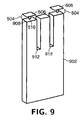
- FIG. 9 is a perspective view of a doubly-slotted capacitively back-coupled handset having two feeds
- FIG. 10 is a graph of simulated return loss S 11 in dB against frequency f in MHz for one feed of the handset of FIG. 9;
- FIG. 11 is a Smith chart showing the simulated impedance of one feed of the handset of FIG. 9 over the frequency range 1000 to 2800 MHz;
- FIG. 12 is a graph of simulated return loss S 11 in dB against frequency f in MHz for one feed of the handset of FIG. 9 with additional matching;
- FIG. 13 is a Smith chart showing the simulated impedance of one feed of the handset of FIG. 9, with additional matching, over the frequency range 1000 to 2800 MHz;
- FIG. 14 is a graph of simulated return loss S11 in dB against frequency f in MHz for one feed of the handset of FIG. 9 with additional matching and held in a hand;
- FIG. 15 is a Smith chart showing the simulated impedance of one feed of the handset of FIG. 9, with additional matching and held in a hand, over the frequency range 1000 to 2800 MHz.
- FIG. 1 shows a model of the impedance seen by a transceiver, in transmit mode, in a wireless handset at its antenna feed point.
- the impedance is modelled as an asymmetrical dipole, where the first arm 102 represents the impedance of the antenna and the second arm 104 the impedance of the handset, both arms being driven by a source 106 .
- the impedance of such an arrangement is substantially equivalent to the sum of the impedance of each arm 102 , 104 driven separately against a virtual ground 108 .
- the model could equally well be used for reception by replacing the source 106 by an impedance representing that of the transceiver, although this is rather more difficult to simulate.
- FIG. 2 shows the results for the real and imaginary parts of the impedance (R+jX) of the combined arrangement (Ref R and Ref X) together with results obtained by simulating the impedances separately and summing the result. It can be seen that the results of the simulations are quite close. The only significant deviation is in the region of half-wave resonance, when the impedance is difficult to simulate accurately.
- the antenna If the size of the antenna is reduced, its radiation resistance R 1 will also reduce. If the antenna becomes infinitesimally small its radiation resistance R 1 will fall to zero and all of the radiation will come from the handset. This situation can be made beneficial if the handset impedance is suitable for the source 106 driving it and if the capacitive reactance of the infinitesimal antenna can be minimised by increasing the capacitive back-coupling to the handset.
- the equivalent circuit is modified to that shown in FIG. 4 .
- the antenna has therefore been replaced with a physically very small back-coupling capacitor, designed to have a large capacitance for maximum coupling and minimum reactance.
- the residual reactance of the back-coupling capacitor can be tuned out with a simple matching circuit.
- the resulting bandwidth can be much greater than with a conventional antenna and handset combination, because the handset acts as a low Q radiating element (simulations show that a typical Q is around 1), whereas conventional antennas typically have a Q of around 50.
- a basic embodiment of a capacitively back-coupled handset is shown in FIG. 5.
- a handset 502 has dimensions of 10 ⁇ 40 ⁇ 100 mm, typical of modern cellular handsets.
- a parallel plate capacitor 504 having dimensions 2 ⁇ 10 ⁇ 10 mm, is formed by mounting a 10 ⁇ 10 mm plate 506 2 mm above the top edge 508 of the handset 502 , in the position normally occupied by a much larger antenna.
- the resultant capacitance is about 0.5 pF, representing a compromise between capacitance (which would be increased by reducing the separation of the handset 502 and plate 506 ) and coupling effectiveness (which depends on the separation of the handset 502 and plate 506 ).
- the capacitor is fed via a support 510 , which is insulated from the handset case 502 .
- the return loss S 11 of this embodiment after matching was simulated using the High Frequency Structure Simulator (HFSS), available from Ansoft Corporation, with the results shown in FIG. 6 for frequencies f between 1000 and 2800 MHz.
- HFSS High Frequency Structure Simulator
- a conventional two inductor “L” network was used to match at 1900 MHz.
- the resultant bandwidth at 7 dB return loss (corresponding to approximately 90% of input power radiated) is approximately 60 MHz, or 3%, which is useful but not as large as was required.
- a Smith chart illustrating the simulated impedance of this embodiment over the same frequency range is shown in FIG. 7 .
- FIG. 8 shows the resistance variation, over the same frequency range as before, simulated using HFSS. This can be improved by redesigning the case to increase the resistance, for example by the use of a slot or a narrower handset, as discussed in our co-pending unpublished United Kingdom patent application 0019335.9
- a diversity handset 902 has a conducting case having dimensions of 10 ⁇ 40 ⁇ 100 mm, into which two slots 912 have been cut. Each slot 912 has a width of 3 mm and a depth of 29.5 mm and is placed 12 mm in from a side of the handset 902 .
- a capacitor 504 is formed from a plate 506 , having dimensions 10 ⁇ 10 mm, mounted 4 mm above the top surface 908 of the handset 902 on a support 510 .
- the return loss S 11 of this embodiment was simulated using HFSS, with the results shown in FIG. 10 for frequencies f between 1000 and 2800 MHz.
- one capacitor 504 was fed directly, without matching, while the other capacitor 504 was left open circuit.
- the first resonance is similar to that which would be achieved if only one capacitor 504 and slot 912 were present, as shown in our co-pending unpublished UK patent application 0019335.9.
- the second resonance is due to the presence of an additional slot 912 .
- the centre frequency of the first resonance is reduced by the presence of a second slot 912 , and hence the length of the slots 912 is reduced compared to an embodiment having a single slot.
- a Smith chart illustrating the simulated impedance of this embodiment over the same frequency range is shown in FIG. 11 . The rapid changes in impedance in the Smith chart reflect the narrow-band nature of the second resonance.
- the response of this embodiment can be improved by matching. Simulations were performed using a similar two inductor matching network to that employed in the basic embodiment, but matching both feeds simultaneously. This would be used in a dual receiver diversity architecture, where both antennas are available simultaneously. Similar performance could be obtained with one feed connected and matched while the other is disconnected or loaded with another impedance, as would be used in a switched diversity configuration.
- Results for the return loss S 11 are shown in FIG. 12 for frequencies f between 1000 and 2800 MHz.
- the resultant bandwidth at 7 dB return loss is now approximately 750 MHz, or nearly 40%. This is more than enough to cover UMTS and DCS 1800 bands simultaneously, which require coverage from 1710 to 2170 MHz.
- a Smith chart illustrating the simulated impedance of this embodiment over the same frequency range is shown in FIG. 13 .
- the diversity embodiment described above made use of slots 912 in the handset case 902 to enhance the feed match for coverage of both DCS1800 and UMTS bands.
- Other embodiments are possible (including those without handset slots) which may trade off bandwidth against volume for example.
- slots When slots are provided, they may be extended to run the full length of the handset, and additional slots may also be provided for enhanced multi-band operation.
- the function of the slots 912 in the diversity embodiment described above is to provide an impedance transformation so that the antenna feed provides a reasonable match to 50 ⁇ . Adequate diversity performance should be achieved providing that the antenna feeds are separated sufficiently on the ground conductor 902 (for example those in FIG. 9 are separated by approximately 0.2 wavelengths at 1711 MHz).
- any other sacrificial (non-radiating) coupling element could be used instead, for example inductive coupling.
- the coupling element could be altered in order to aid impedance matching.
- capacitive coupling could be achieved via an inductive element. This would allow easier matching to yield a more wideband response.
- a conducting handset case has been the radiating element.
- other ground conductors in a wireless terminal could perform a similar function. Examples include conductors used for EMC shielding and an area of Printed Circuit Board (PCB) metallisation, for example a ground plane.
- PCB Printed Circuit Board
Abstract
Description

| Frequency (MHz) | ||
| Environment | 1711 | 1918 | 2170 | ||
| rural | 0.58 | 0.21 | 0.63 | ||
| suburban | 0.46 | 0.10 | 0.51 | ||
| urban macro/microcell | 0.45 | 0.10 | 0.50 | ||
| urban picocell | 0.46 | 0.11 | 0.51 | ||
| outdoors to indoors | 0.34 | 0.04 | 0.37 | ||
| indoors | 0.35 | 0.05 | 0.39 | ||
| Frequency (MHz) | ||
| Environment | 1711 | 1918 | 2170 | ||
| rural | 0.21 | 0.04 | 0.45 | ||
| suburban | 0.14 | 0.05 | 0.46 | ||
| urban macro/microcell | 0.18 | 0.06 | 0.45 | ||
| urban picocell | 0.10 | 0.00 | 0.38 | ||
| outdoors to indoors | 0.06 | 0.02 | 0.30 | ||
| indoors | 0.09 | 0.01 | 0.31 | ||
Claims (7)
Applications Claiming Priority (3)
| Application Number | Priority Date | Filing Date | Title |
|---|---|---|---|
| GBGB0102768.9A GB0102768D0 (en) | 2001-02-02 | 2001-02-02 | Wireless terminal |
| GB0102768 | 2001-02-02 | ||
| GB0102768.9 | 2001-02-02 |
Publications (2)
| Publication Number | Publication Date |
|---|---|
| US20020180648A1 US20020180648A1 (en) | 2002-12-05 |
| US6791498B2 true US6791498B2 (en) | 2004-09-14 |
Family
ID=9908090
Family Applications (1)
| Application Number | Title | Priority Date | Filing Date |
|---|---|---|---|
| US10/055,386 Expired - Lifetime US6791498B2 (en) | 2001-02-02 | 2002-01-23 | Wireless terminal |
Country Status (10)
| Country | Link |
|---|---|
| US (1) | US6791498B2 (en) |
| EP (1) | EP1360740B1 (en) |
| JP (1) | JP4347567B2 (en) |
| KR (1) | KR100903445B1 (en) |
| CN (1) | CN100492759C (en) |
| AT (1) | ATE451733T1 (en) |
| DE (1) | DE60234680D1 (en) |
| GB (1) | GB0102768D0 (en) |
| TW (1) | TW567640B (en) |
| WO (1) | WO2002063712A1 (en) |
Cited By (20)
| Publication number | Priority date | Publication date | Assignee | Title |
|---|---|---|---|---|
| US20040058723A1 (en) * | 2002-09-19 | 2004-03-25 | Filtronic Lk Oy | Internal atenna |
| US20050259013A1 (en) * | 2002-06-25 | 2005-11-24 | David Gala Gala | Multiband antenna for handheld terminal |
| US20060205350A1 (en) * | 2002-12-11 | 2006-09-14 | Goggin Christopher M | Master signal transmitter with allied servant receiver to receive a directed signal from the transmitter |
| US20080062055A1 (en) * | 2006-09-11 | 2008-03-13 | Elster Electricity, Llc | Printed circuit notch antenna |
| US20080084356A1 (en) * | 2006-10-06 | 2008-04-10 | Sony Ericsson Mobile Communications Ab | Antenna for portable communication device |
| US20090079655A1 (en) * | 2007-09-21 | 2009-03-26 | Samsung Electronics Co., Ltd. | Multi-band antenna and multi-band antenna system with enhanced isolation characteristic |
| US20090207092A1 (en) * | 2008-02-15 | 2009-08-20 | Paul Nysen | Compact diversity antenna system |
| US20090318094A1 (en) * | 2006-06-08 | 2009-12-24 | Fractus, S.A. | Distributed antenna system robust to human body loading effects |
| US20100134350A1 (en) * | 2007-10-09 | 2010-06-03 | Qualcomm Incorporated | Apparatus including housing incorporating a radiating element of an antenna |
| US20100176999A1 (en) * | 2008-08-04 | 2010-07-15 | Fractus, S.A. | Antennaless wireless device capable of operation in multiple frequency regions |
| US20100238079A1 (en) * | 2009-03-17 | 2010-09-23 | Mina Ayatollahi | High isolation multiple port antenna array handheld mobile communication devices |
| US20100238072A1 (en) * | 2009-03-17 | 2010-09-23 | Mina Ayatollahi | Wideband, high isolation two port antenna array for multiple input, multiple output handheld devices |
| US7903034B2 (en) | 2005-09-19 | 2011-03-08 | Fractus, S.A. | Antenna set, portable wireless device, and use of a conductive element for tuning the ground-plane of the antenna set |
| US8203492B2 (en) | 2008-08-04 | 2012-06-19 | Fractus, S.A. | Antennaless wireless device |
| US8952855B2 (en) | 2010-08-03 | 2015-02-10 | Fractus, S.A. | Wireless device capable of multiband MIMO operation |
| US9147929B2 (en) | 2010-02-02 | 2015-09-29 | Fractus, S.A. | Antennaless wireless device comprising one or more bodies |
| US9331389B2 (en) | 2012-07-16 | 2016-05-03 | Fractus Antennas, S.L. | Wireless handheld devices, radiation systems and manufacturing methods |
| US9379443B2 (en) | 2012-07-16 | 2016-06-28 | Fractus Antennas, S.L. | Concentrated wireless device providing operability in multiple frequency regions |
| US9960478B2 (en) | 2014-07-24 | 2018-05-01 | Fractus Antennas, S.L. | Slim booster bars for electronic devices |
| US10374285B2 (en) * | 2013-08-27 | 2019-08-06 | Nec Platforms, Ltd | Antenna and wireless communication apparatus |
Families Citing this family (13)
| Publication number | Priority date | Publication date | Assignee | Title |
|---|---|---|---|---|
| GB0122226D0 (en) | 2001-09-13 | 2001-11-07 | Koninl Philips Electronics Nv | Wireless terminal |
| CN100530987C (en) * | 2004-03-04 | 2009-08-19 | 株式会社村田制作所 | Antenna device and radio communication device using the same |
| JP3841100B2 (en) * | 2004-07-06 | 2006-11-01 | セイコーエプソン株式会社 | Electronic device and wireless communication terminal |
| JP4651110B2 (en) * | 2006-03-07 | 2011-03-16 | 国立大学法人横浜国立大学 | Small portable terminal device for wireless reception |
| JP4738380B2 (en) * | 2007-05-10 | 2011-08-03 | 株式会社東芝 | Electronics |
| JP5262831B2 (en) * | 2009-02-26 | 2013-08-14 | 株式会社日本自動車部品総合研究所 | In-vehicle antenna device |
| JP5573358B2 (en) * | 2010-05-20 | 2014-08-20 | 株式会社リコー | ANTENNA DEVICE AND WIRELESS COMMUNICATION DEVICE USING THE SAME |
| CN102110900B (en) * | 2010-12-27 | 2014-07-02 | 中兴通讯股份有限公司 | Array antenna of mobile terminal and implementation method of array antenna |
| WO2013011339A1 (en) * | 2011-07-18 | 2013-01-24 | Sony Ericsson Mobile Communications Ab | Multi-band wireless terminals with metal backplates and coupling feed elements, and related multi-band antenna systems |
| US9300033B2 (en) | 2011-10-21 | 2016-03-29 | Futurewei Technologies, Inc. | Wireless communication device with an antenna adjacent to an edge of the device |
| US8884835B2 (en) * | 2012-08-09 | 2014-11-11 | Intel Mobile Communications GmbH | Antenna system, method and mobile communication device |
| KR101977078B1 (en) * | 2012-08-10 | 2019-05-10 | 엘지전자 주식회사 | Mobile terminal |
| US10637444B1 (en) * | 2018-12-21 | 2020-04-28 | Northrop Gruman Systems Corporation | Near field RFID probe with tunning |
Citations (9)
| Publication number | Priority date | Publication date | Assignee | Title |
|---|---|---|---|---|
| US4876552A (en) * | 1988-04-27 | 1989-10-24 | Motorola, Inc. | Internally mounted broadband antenna |
| US5903822A (en) | 1991-12-26 | 1999-05-11 | Kabushiki Kaisha Toshiba | Portable radio and telephones having notches therein |
| US5977916A (en) | 1997-05-09 | 1999-11-02 | Motorola, Inc. | Difference drive diversity antenna structure and method |
| US6002367A (en) * | 1996-05-17 | 1999-12-14 | Allgon Ab | Planar antenna device |
| US6140966A (en) * | 1997-07-08 | 2000-10-31 | Nokia Mobile Phones Limited | Double resonance antenna structure for several frequency ranges |
| US6204817B1 (en) * | 1998-09-28 | 2001-03-20 | Allgon Ab | Radio communication device and an antenna system |
| EP1094542A2 (en) | 1999-10-18 | 2001-04-25 | Matsushita Electric Industrial Co., Ltd. | Antenna for mobile wireless communicatios and portable-type wireless apparatus using the same |
| US6414637B2 (en) * | 2000-02-04 | 2002-07-02 | Rangestar Wireless Inc. | Dual frequency wideband radiator |
| US6424300B1 (en) * | 2000-10-27 | 2002-07-23 | Telefonaktiebolaget L.M. Ericsson | Notch antennas and wireless communicators incorporating same |
Family Cites Families (1)
| Publication number | Priority date | Publication date | Assignee | Title |
|---|---|---|---|---|
| JPH05259725A (en) * | 1992-03-16 | 1993-10-08 | Sharp Corp | Diversity antenna for portable radio equipment |
-
2001
- 2001-02-02 GB GBGB0102768.9A patent/GB0102768D0/en not_active Ceased
-
2002
- 2002-01-15 EP EP02740052A patent/EP1360740B1/en not_active Expired - Lifetime
- 2002-01-15 DE DE60234680T patent/DE60234680D1/en not_active Expired - Lifetime
- 2002-01-15 WO PCT/IB2002/000102 patent/WO2002063712A1/en active Application Filing
- 2002-01-15 JP JP2002563554A patent/JP4347567B2/en not_active Expired - Fee Related
- 2002-01-15 KR KR1020027013179A patent/KR100903445B1/en active IP Right Grant
- 2002-01-15 CN CNB028002253A patent/CN100492759C/en not_active Expired - Fee Related
- 2002-01-15 AT AT02740052T patent/ATE451733T1/en not_active IP Right Cessation
- 2002-01-23 US US10/055,386 patent/US6791498B2/en not_active Expired - Lifetime
- 2002-01-29 TW TW091101500A patent/TW567640B/en not_active IP Right Cessation
Patent Citations (9)
| Publication number | Priority date | Publication date | Assignee | Title |
|---|---|---|---|---|
| US4876552A (en) * | 1988-04-27 | 1989-10-24 | Motorola, Inc. | Internally mounted broadband antenna |
| US5903822A (en) | 1991-12-26 | 1999-05-11 | Kabushiki Kaisha Toshiba | Portable radio and telephones having notches therein |
| US6002367A (en) * | 1996-05-17 | 1999-12-14 | Allgon Ab | Planar antenna device |
| US5977916A (en) | 1997-05-09 | 1999-11-02 | Motorola, Inc. | Difference drive diversity antenna structure and method |
| US6140966A (en) * | 1997-07-08 | 2000-10-31 | Nokia Mobile Phones Limited | Double resonance antenna structure for several frequency ranges |
| US6204817B1 (en) * | 1998-09-28 | 2001-03-20 | Allgon Ab | Radio communication device and an antenna system |
| EP1094542A2 (en) | 1999-10-18 | 2001-04-25 | Matsushita Electric Industrial Co., Ltd. | Antenna for mobile wireless communicatios and portable-type wireless apparatus using the same |
| US6414637B2 (en) * | 2000-02-04 | 2002-07-02 | Rangestar Wireless Inc. | Dual frequency wideband radiator |
| US6424300B1 (en) * | 2000-10-27 | 2002-07-23 | Telefonaktiebolaget L.M. Ericsson | Notch antennas and wireless communicators incorporating same |
Non-Patent Citations (1)
| Title |
|---|
| PHGB 010056 Paten Application (Pending), Ser. No.: 09/912,470, Entitled: Wireless Terminal, Inventors Kevin R. Boyle et la. |
Cited By (57)
| Publication number | Priority date | Publication date | Assignee | Title |
|---|---|---|---|---|
| US20050259013A1 (en) * | 2002-06-25 | 2005-11-24 | David Gala Gala | Multiband antenna for handheld terminal |
| US7486242B2 (en) | 2002-06-25 | 2009-02-03 | Fractus, S.A. | Multiband antenna for handheld terminal |
| US7903037B2 (en) | 2002-06-25 | 2011-03-08 | Fractus, S.A. | Multiband antenna for handheld terminal |
| US6985108B2 (en) * | 2002-09-19 | 2006-01-10 | Filtronic Lk Oy | Internal antenna |
| US20040058723A1 (en) * | 2002-09-19 | 2004-03-25 | Filtronic Lk Oy | Internal atenna |
| US20060205350A1 (en) * | 2002-12-11 | 2006-09-14 | Goggin Christopher M | Master signal transmitter with allied servant receiver to receive a directed signal from the transmitter |
| US7903034B2 (en) | 2005-09-19 | 2011-03-08 | Fractus, S.A. | Antenna set, portable wireless device, and use of a conductive element for tuning the ground-plane of the antenna set |
| US8138981B2 (en) | 2005-09-19 | 2012-03-20 | Fractus, S.A. | Antenna set, portable wireless device, and use of a conductive element for tuning the ground-plane of the antenna set |
| US20110175776A1 (en) * | 2005-09-19 | 2011-07-21 | Jaume Anguera | Antenna set, portable wireless device, and use of a conductive element for tuning the ground-plane of the antenna set |
| US20090318094A1 (en) * | 2006-06-08 | 2009-12-24 | Fractus, S.A. | Distributed antenna system robust to human body loading effects |
| US10033114B2 (en) | 2006-06-08 | 2018-07-24 | Fractus Antennas, S.L. | Distributed antenna system robust to human body loading effects |
| US10411364B2 (en) | 2006-06-08 | 2019-09-10 | Fractus Antennas, S.L. | Distributed antenna system robust to human body loading effects |
| US9007275B2 (en) | 2006-06-08 | 2015-04-14 | Fractus, S.A. | Distributed antenna system robust to human body loading effects |
| US7696941B2 (en) | 2006-09-11 | 2010-04-13 | Elster Electricity, Llc | Printed circuit notch antenna |
| US20080062055A1 (en) * | 2006-09-11 | 2008-03-13 | Elster Electricity, Llc | Printed circuit notch antenna |
| US7701398B2 (en) * | 2006-10-06 | 2010-04-20 | Sony Ericsson Mobile Communications Ab | Antenna for portable communication device |
| US20080084356A1 (en) * | 2006-10-06 | 2008-04-10 | Sony Ericsson Mobile Communications Ab | Antenna for portable communication device |
| US20090079655A1 (en) * | 2007-09-21 | 2009-03-26 | Samsung Electronics Co., Ltd. | Multi-band antenna and multi-band antenna system with enhanced isolation characteristic |
| US8009102B2 (en) * | 2007-09-21 | 2011-08-30 | Samsung Electronics Co., Ltd. | Multi-band antenna and multi-band antenna system with enhanced isolation characteristic |
| US8538345B2 (en) * | 2007-10-09 | 2013-09-17 | Qualcomm Incorporated | Apparatus including housing incorporating a radiating element of an antenna |
| US20100134350A1 (en) * | 2007-10-09 | 2010-06-03 | Qualcomm Incorporated | Apparatus including housing incorporating a radiating element of an antenna |
| US20090207092A1 (en) * | 2008-02-15 | 2009-08-20 | Paul Nysen | Compact diversity antenna system |
| US7724201B2 (en) | 2008-02-15 | 2010-05-25 | Sierra Wireless, Inc. | Compact diversity antenna system |
| US9761944B2 (en) | 2008-08-04 | 2017-09-12 | Fractus Antennas, S.L. | Antennaless wireless device |
| US11183761B2 (en) | 2008-08-04 | 2021-11-23 | Ignion, S.L. | Antennaless wireless device capable of operation in multiple frequency regions |
| US8203492B2 (en) | 2008-08-04 | 2012-06-19 | Fractus, S.A. | Antennaless wireless device |
| US10763585B2 (en) | 2008-08-04 | 2020-09-01 | Fractus Antennas, S.L. | Antennaless wireless device capable of operation in multiple frequency regions |
| US8736497B2 (en) | 2008-08-04 | 2014-05-27 | Fractus, S.A. | Antennaless wireless device capable of operation in multiple frequency regions |
| US11139574B2 (en) | 2008-08-04 | 2021-10-05 | Ignion, S.L. | Antennaless wireless device |
| US10734724B2 (en) | 2008-08-04 | 2020-08-04 | Fractus Antennas, S.L. | Antennaless wireless device |
| US8237615B2 (en) | 2008-08-04 | 2012-08-07 | Fractus, S.A. | Antennaless wireless device capable of operation in multiple frequency regions |
| US11557827B2 (en) | 2008-08-04 | 2023-01-17 | Ignion, S.L. | Antennaless wireless device |
| US9130259B2 (en) | 2008-08-04 | 2015-09-08 | Fractus, S.A. | Antennaless wireless device |
| US10249952B2 (en) | 2008-08-04 | 2019-04-02 | Fractus Antennas, S.L. | Antennaless wireless device capable of operation in multiple frequency regions |
| US9276307B2 (en) | 2008-08-04 | 2016-03-01 | Fractus Antennas, S.L. | Antennaless wireless device |
| US20100176999A1 (en) * | 2008-08-04 | 2010-07-15 | Fractus, S.A. | Antennaless wireless device capable of operation in multiple frequency regions |
| US9350070B2 (en) | 2008-08-04 | 2016-05-24 | Fractus Antennas, S.L. | Antennaless wireless device capable of operation in multiple frequency regions |
| US9960490B2 (en) | 2008-08-04 | 2018-05-01 | Fractus Antennas, S.L. | Antennaless wireless device capable of operation in multiple frequency regions |
| US8933842B2 (en) | 2009-03-17 | 2015-01-13 | Blackberry Limited | Wideband, high isolation two port antenna array for multiple input, multiple output handheld devices |
| US20100238079A1 (en) * | 2009-03-17 | 2010-09-23 | Mina Ayatollahi | High isolation multiple port antenna array handheld mobile communication devices |
| US20100238072A1 (en) * | 2009-03-17 | 2010-09-23 | Mina Ayatollahi | Wideband, high isolation two port antenna array for multiple input, multiple output handheld devices |
| US8085202B2 (en) * | 2009-03-17 | 2011-12-27 | Research In Motion Limited | Wideband, high isolation two port antenna array for multiple input, multiple output handheld devices |
| US8552913B2 (en) | 2009-03-17 | 2013-10-08 | Blackberry Limited | High isolation multiple port antenna array handheld mobile communication devices |
| US9147929B2 (en) | 2010-02-02 | 2015-09-29 | Fractus, S.A. | Antennaless wireless device comprising one or more bodies |
| US8952855B2 (en) | 2010-08-03 | 2015-02-10 | Fractus, S.A. | Wireless device capable of multiband MIMO operation |
| US9112284B2 (en) | 2010-08-03 | 2015-08-18 | Fractus, S.A. | Wireless device capable of multiband MIMO operation |
| US9997841B2 (en) | 2010-08-03 | 2018-06-12 | Fractus Antennas, S.L. | Wireless device capable of multiband MIMO operation |
| US10749246B2 (en) | 2012-07-16 | 2020-08-18 | Fractus Antennas, S.L. | Wireless handheld devices, radiation systems and manufacturing methods |
| US10833411B2 (en) | 2012-07-16 | 2020-11-10 | Fractus Antennas, S.L. | Concentrated wireless device providing operability in multiple frequency regions |
| US9331389B2 (en) | 2012-07-16 | 2016-05-03 | Fractus Antennas, S.L. | Wireless handheld devices, radiation systems and manufacturing methods |
| US11450945B2 (en) | 2012-07-16 | 2022-09-20 | Ignion, S.L. | Wireless handheld devices, radiation systems and manufacturing methods |
| US9379443B2 (en) | 2012-07-16 | 2016-06-28 | Fractus Antennas, S.L. | Concentrated wireless device providing operability in multiple frequency regions |
| US11626665B2 (en) | 2012-07-16 | 2023-04-11 | Ignion, S.L. | Concentrated wireless device providing operability in multiple frequency regions |
| US10374285B2 (en) * | 2013-08-27 | 2019-08-06 | Nec Platforms, Ltd | Antenna and wireless communication apparatus |
| US9960478B2 (en) | 2014-07-24 | 2018-05-01 | Fractus Antennas, S.L. | Slim booster bars for electronic devices |
| US10236561B2 (en) | 2014-07-24 | 2019-03-19 | Fractus Antennas, S.L. | Slim booster bars for electronic devices |
| US11349195B2 (en) | 2014-07-24 | 2022-05-31 | Ignion, S.L. | Slim booster bars for electronic devices |
Also Published As
| Publication number | Publication date |
|---|---|
| JP4347567B2 (en) | 2009-10-21 |
| KR100903445B1 (en) | 2009-06-18 |
| EP1360740B1 (en) | 2009-12-09 |
| CN1455971A (en) | 2003-11-12 |
| WO2002063712A1 (en) | 2002-08-15 |
| ATE451733T1 (en) | 2009-12-15 |
| JP2004519148A (en) | 2004-06-24 |
| CN100492759C (en) | 2009-05-27 |
| EP1360740A1 (en) | 2003-11-12 |
| GB0102768D0 (en) | 2001-03-21 |
| DE60234680D1 (en) | 2010-01-21 |
| US20020180648A1 (en) | 2002-12-05 |
| KR20020084283A (en) | 2002-11-04 |
| TW567640B (en) | 2003-12-21 |
Similar Documents
| Publication | Publication Date | Title |
|---|---|---|
| US6791498B2 (en) | Wireless terminal | |
| US7058434B2 (en) | Mobile communication | |
| US6552686B2 (en) | Internal multi-band antenna with improved radiation efficiency | |
| CN101512835B (en) | Multiband antenna arrangement | |
| US6980154B2 (en) | Planar inverted F antennas including current nulls between feed and ground couplings and related communications devices | |
| EP1293012B1 (en) | Dual band patch antenna | |
| US7256743B2 (en) | Internal multiband antenna | |
| EP1506594B1 (en) | Antenna arrangement and module including the arrangement | |
| US6225951B1 (en) | Antenna systems having capacitively coupled internal and retractable antennas and wireless communicators incorporating same | |
| WO2003077360A1 (en) | Multiband planar built-in radio antenna with inverted-l main and parasitic radiators | |
| EP1368855A1 (en) | Antenna arrangement | |
| WO2011161550A2 (en) | Distributed multiband antenna and methods | |
| US7835776B2 (en) | Wireless terminal | |
| US20020171590A1 (en) | Antenna arrangement | |
| US7522936B2 (en) | Wireless terminal | |
| Ozbakis et al. | Multi-band frequency tunable LTE antenna for mobile phone applications |
Legal Events
| Date | Code | Title | Description |
|---|---|---|---|
| AS | Assignment |
Owner name: KONINKLIJKE PHILIPS ELECTRONICS N.V., NETHERLANDS Free format text: ASSIGNMENT OF ASSIGNORS INTEREST;ASSIGNORS:BOYLE, KEVIN R.;MASSEY, PETER J.;REEL/FRAME:012579/0526;SIGNING DATES FROM 20011205 TO 20011206 |
|
| STCF | Information on status: patent grant |
Free format text: PATENTED CASE |
|
| AS | Assignment |
Owner name: NXP B.V., NETHERLANDS Free format text: ASSIGNMENT OF ASSIGNORS INTEREST;ASSIGNOR:KONINKLIJKE PHILIPS ELECTRONICS N.V.;REEL/FRAME:018635/0787 Effective date: 20061117 |
|
| AS | Assignment |
Owner name: MORGAN STANLEY SENIOR FUNDING, INC., ENGLAND Free format text: SECURITY AGREEMENT;ASSIGNOR:NXP B.V.;REEL/FRAME:018806/0201 Effective date: 20061201 |
|
| FPAY | Fee payment |
Year of fee payment: 4 |
|
| AS | Assignment |
Owner name: CALLAHAN CELLULAR L.L.C., DELAWARE Free format text: ASSIGNMENT OF ASSIGNORS INTEREST;ASSIGNOR:NXP B.V.;REEL/FRAME:027265/0798 Effective date: 20110926 |
|
| FEPP | Fee payment procedure |
Free format text: PAYOR NUMBER ASSIGNED (ORIGINAL EVENT CODE: ASPN); ENTITY STATUS OF PATENT OWNER: LARGE ENTITY Free format text: PAYER NUMBER DE-ASSIGNED (ORIGINAL EVENT CODE: RMPN); ENTITY STATUS OF PATENT OWNER: LARGE ENTITY |
|
| FPAY | Fee payment |
Year of fee payment: 8 |
|
| AS | Assignment |
Owner name: NXP B.V., NETHERLANDS Free format text: RELEASE BY SECURED PARTY;ASSIGNOR:MORGAN STANLEY SENIOR FUNDING, INC.;REEL/FRAME:028162/0004 Effective date: 20110930 |
|
| FPAY | Fee payment |
Year of fee payment: 12 |
|
| AS | Assignment |
Owner name: NXP B.V., NETHERLANDS Free format text: RELEASE BY SECURED PARTY;ASSIGNOR:MORGAN STANLEY SENIOR FUNDING, INC;REEL/FRAME:050315/0443 Effective date: 20190903 |
|
| AS | Assignment |
Owner name: INTELLECTUAL VENTURES ASSETS 186 LLC, DELAWARE Free format text: ASSIGNMENT OF ASSIGNORS INTEREST;ASSIGNOR:CALLAHAN CELLULAR L.L.C.;REEL/FRAME:062708/0463 Effective date: 20221222 |
|
| AS | Assignment |
Owner name: INTELLECTUAL VENTURES ASSETS 186 LLC, DELAWARE Free format text: SECURITY INTEREST;ASSIGNOR:MIND FUSION, LLC;REEL/FRAME:063295/0001 Effective date: 20230214 Owner name: INTELLECTUAL VENTURES ASSETS 191 LLC, DELAWARE Free format text: SECURITY INTEREST;ASSIGNOR:MIND FUSION, LLC;REEL/FRAME:063295/0001 Effective date: 20230214 |
|
| AS | Assignment |
Owner name: MIND FUSION, LLC, WASHINGTON Free format text: ASSIGNMENT OF ASSIGNORS INTEREST;ASSIGNOR:INTELLECTUAL VENTURES ASSETS 186 LLC;REEL/FRAME:064271/0001 Effective date: 20230214 |