US6801157B2 - Guided wave radar level transmitter - Google Patents
Guided wave radar level transmitter Download PDFInfo
- Publication number
- US6801157B2 US6801157B2 US10/642,257 US64225703A US6801157B2 US 6801157 B2 US6801157 B2 US 6801157B2 US 64225703 A US64225703 A US 64225703A US 6801157 B2 US6801157 B2 US 6801157B2
- Authority
- US
- United States
- Prior art keywords
- probe
- transmission line
- circuit
- signal
- ramp
- Prior art date
- Legal status (The legal status is an assumption and is not a legal conclusion. Google has not performed a legal analysis and makes no representation as to the accuracy of the status listed.)
- Expired - Lifetime
Links
Images


Classifications
-
- G—PHYSICS
- G01—MEASURING; TESTING
- G01S—RADIO DIRECTION-FINDING; RADIO NAVIGATION; DETERMINING DISTANCE OR VELOCITY BY USE OF RADIO WAVES; LOCATING OR PRESENCE-DETECTING BY USE OF THE REFLECTION OR RERADIATION OF RADIO WAVES; ANALOGOUS ARRANGEMENTS USING OTHER WAVES
- G01S13/00—Systems using the reflection or reradiation of radio waves, e.g. radar systems; Analogous systems using reflection or reradiation of waves whose nature or wavelength is irrelevant or unspecified
- G01S13/02—Systems using reflection of radio waves, e.g. primary radar systems; Analogous systems
- G01S13/06—Systems determining position data of a target
- G01S13/08—Systems for measuring distance only
- G01S13/10—Systems for measuring distance only using transmission of interrupted, pulse modulated waves
- G01S13/103—Systems for measuring distance only using transmission of interrupted, pulse modulated waves particularities of the measurement of the distance
-
- G—PHYSICS
- G01—MEASURING; TESTING
- G01F—MEASURING VOLUME, VOLUME FLOW, MASS FLOW OR LIQUID LEVEL; METERING BY VOLUME
- G01F23/00—Indicating or measuring liquid level or level of fluent solid material, e.g. indicating in terms of volume or indicating by means of an alarm
- G01F23/22—Indicating or measuring liquid level or level of fluent solid material, e.g. indicating in terms of volume or indicating by means of an alarm by measuring physical variables, other than linear dimensions, pressure or weight, dependent on the level to be measured, e.g. by difference of heat transfer of steam or water
- G01F23/28—Indicating or measuring liquid level or level of fluent solid material, e.g. indicating in terms of volume or indicating by means of an alarm by measuring physical variables, other than linear dimensions, pressure or weight, dependent on the level to be measured, e.g. by difference of heat transfer of steam or water by measuring the variations of parameters of electromagnetic or acoustic waves applied directly to the liquid or fluent solid material
- G01F23/284—Electromagnetic waves
-
- G—PHYSICS
- G01—MEASURING; TESTING
- G01S—RADIO DIRECTION-FINDING; RADIO NAVIGATION; DETERMINING DISTANCE OR VELOCITY BY USE OF RADIO WAVES; LOCATING OR PRESENCE-DETECTING BY USE OF THE REFLECTION OR RERADIATION OF RADIO WAVES; ANALOGOUS ARRANGEMENTS USING OTHER WAVES
- G01S13/00—Systems using the reflection or reradiation of radio waves, e.g. radar systems; Analogous systems using reflection or reradiation of waves whose nature or wavelength is irrelevant or unspecified
- G01S13/02—Systems using reflection of radio waves, e.g. primary radar systems; Analogous systems
- G01S13/0209—Systems with very large relative bandwidth, i.e. larger than 10 %, e.g. baseband, pulse, carrier-free, ultrawideband
-
- G—PHYSICS
- G01—MEASURING; TESTING
- G01S—RADIO DIRECTION-FINDING; RADIO NAVIGATION; DETERMINING DISTANCE OR VELOCITY BY USE OF RADIO WAVES; LOCATING OR PRESENCE-DETECTING BY USE OF THE REFLECTION OR RERADIATION OF RADIO WAVES; ANALOGOUS ARRANGEMENTS USING OTHER WAVES
- G01S13/00—Systems using the reflection or reradiation of radio waves, e.g. radar systems; Analogous systems using reflection or reradiation of waves whose nature or wavelength is irrelevant or unspecified
- G01S13/88—Radar or analogous systems specially adapted for specific applications
-
- G—PHYSICS
- G01—MEASURING; TESTING
- G01S—RADIO DIRECTION-FINDING; RADIO NAVIGATION; DETERMINING DISTANCE OR VELOCITY BY USE OF RADIO WAVES; LOCATING OR PRESENCE-DETECTING BY USE OF THE REFLECTION OR RERADIATION OF RADIO WAVES; ANALOGOUS ARRANGEMENTS USING OTHER WAVES
- G01S7/00—Details of systems according to groups G01S13/00, G01S15/00, G01S17/00
- G01S7/02—Details of systems according to groups G01S13/00, G01S15/00, G01S17/00 of systems according to group G01S13/00
- G01S7/28—Details of pulse systems
- G01S7/282—Transmitters
-
- G—PHYSICS
- G01—MEASURING; TESTING
- G01S—RADIO DIRECTION-FINDING; RADIO NAVIGATION; DETERMINING DISTANCE OR VELOCITY BY USE OF RADIO WAVES; LOCATING OR PRESENCE-DETECTING BY USE OF THE REFLECTION OR RERADIATION OF RADIO WAVES; ANALOGOUS ARRANGEMENTS USING OTHER WAVES
- G01S7/00—Details of systems according to groups G01S13/00, G01S15/00, G01S17/00
- G01S7/02—Details of systems according to groups G01S13/00, G01S15/00, G01S17/00 of systems according to group G01S13/00
- G01S7/28—Details of pulse systems
- G01S7/285—Receivers
-
- G—PHYSICS
- G01—MEASURING; TESTING
- G01S—RADIO DIRECTION-FINDING; RADIO NAVIGATION; DETERMINING DISTANCE OR VELOCITY BY USE OF RADIO WAVES; LOCATING OR PRESENCE-DETECTING BY USE OF THE REFLECTION OR RERADIATION OF RADIO WAVES; ANALOGOUS ARRANGEMENTS USING OTHER WAVES
- G01S7/00—Details of systems according to groups G01S13/00, G01S15/00, G01S17/00
- G01S7/02—Details of systems according to groups G01S13/00, G01S15/00, G01S17/00 of systems according to group G01S13/00
- G01S7/40—Means for monitoring or calibrating
- G01S7/4004—Means for monitoring or calibrating of parts of a radar system
Definitions
- This invention relates to an apparatus utilizing guided wave radar for measuring the condition or characteristics of a material, and more particularly to improvements in level measurement.
- a very fast stream of pulse with a rise time of 500 picoseconds, or less, is propagated down a transmission line that serves as a probe in a vessel.
- the pulses are reflected by a discontinuity caused by a change in impedance, such as at a transition between two media.
- that transition is typically where the air and the material to be measured meet.
- the transition could be two different liquids.
- the amplitude of the reflected signal depends on the difference between the dielectrics of the two media.
- the dielectric of air is one, while the dielectric of water is about eighty. The larger the difference in dielectric, the larger the reflected signal.
- Guided wave radar is one technique available to measure the level of liquids or solids in an industrial environment using TDR principles.
- Guided wave radar works by generating a stream of pulses of electromagnetic energy and propagating the pulses down a transmission line formed into a level sensing probe.
- the probe is generally placed vertically in a tank or other container and the electromagnetic pulse is launched downward from the top of the probe.
- the probe is open to both the air and the material to be sensed in such a way that the electromagnetic fields of the propagating pulse penetrate the air until they reach the level of the material. At that point, the electromagnetic fields see the higher dielectric of the material. This higher dielectric causes a reduction in the impedance of the transmission line, resulting in a pulse echo being reflected back to the top of the probe.
- the pulse travels through the air dielectric portion of the probe at a known velocity. This allows the material level on the probe to be determined by measuring the round trip travel time of the pulse from the top of the probe to the level and back to the top of the probe. Conductive materials generate echoes similar to the echoes from high dielectric materials. Therefore, the same measurement technique also works with conductive materials.
- Guided wave radar level measuring instruments may use time domain reflectometry for determining level. These instruments use both electrical and electronic circuits to determine level. Some such instruments use complex circuits for implementing the TDR techniques. The complexity of the circuits may require additional components increasing the costs of the resulting devices.
- the present invention is directed to overcoming one or more of the problems discussed above, in a novel and simple manner.
- a process instrument comprising a housing and an active sensing element for sensing a characteristic of a process.
- the control circuit is disposed in the housing and is electrically connected to the active sensing element for measuring the sensed characteristic.
- a safety barrier comprises a blocking capacitor barrier electrically connected between the control circuit and the active sensing element.
- the active sensing element may comprise a guided wave radar transmission line or a capacitance probe.
- the blocking capacitor barrier comprises a plurality of series connected high voltage capacitors.
- a guided wave radar measurement instrument comprising a probe defining a guided wave radar transmission line.
- a pulse circuit is connected to the probe for generating a very fast stream of pulses on the transmission line and receiving reflected pulses returned on the transmission line.
- the reflected pulses represent a characteristic of a material being measured.
- An equivalent time sampling circuit is connected to the pulse circuit operable to sample reflected pulses to build a time multiplied picture of the reflected pulses and comprises a ramp generator circuit generating a saw tooth ramp signal used to selectively delay sampling reflected pulses to build the time multiplied picture.
- the saw tooth ramp signal has a controlled ramp start for each cycle and retrace at an end of the cycle.
- a processing circuit is connected to the equivalent time sampling circuit for selectively controlling ramp start for each cycle and measuring round trip travel time for a pulse from the pulse circuit.
- the ramp generator circuit comprises a latching ramp comparator.
- the latching ramp comparator latches at the end of the cycle and is reset by the processing circuit to start the ramp for each cycle.
- the latching ramp comparator has an output coupled to a non-inverted input.
- the processing circuit resets the latching comparator by applying a low voltage to the non-inverted input.
- the ramp generator circuit comprises a resistor network operatively controlled by the processing circuit for controlling slope of the saw tooth ramp signal.
- a domain reflectometry measurement instrument comprising a probe and a pulse circuit connected to the probe for generating a very fast stream of pulses on the probe and receiving reflective pulses returned on their probe.
- the reflected pulses represent a characteristic of a material being measured.
- An equivalent time sampling circuit is connected to the pulse circuit operable to sample reflected pulses to build a time multiplied picture of the reflected pulses, comprising a ramp generator circuit generating a saw tooth ramp signal used to selectively delay sampling reflected pulses to build the time multiplied picture.
- the ramp generator circuit comprises a ramp comparator that latches at a start voltage during each cycle until receiving a start ramp signal and retraces to the start voltage at an end of the cycle.
- a processing circuit is connected to the equivalent time sampling circuit for selectively generating the start ramp signal for each cycle and measuring round trip travel time for a pulse from the pulse circuit.
- FIG. 1 is a side elevation view of a measurement instrument in accordance with the invention
- FIG. 2 is a block diagram of a control circuit for the instrument of FIG. 1;
- FIG. 3 is a block diagram of the probe interface circuit for the control circuit of FIG. 2;
- FIG. 4 is a block diagram of the signal processing circuit for the control circuit of FIG. 2;
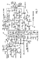
- FIGS. 5 and 6 are a schematic diagram of the probe interface circuit of FIG. 3;
- FIG. 7 is a schematic diagram of the signal processing circuit of FIG. 4.
- FIG. 8 is a timing diagram illustrating operation of the control circuit in accordance with the invention used with a coaxial or twin rod probe.
- FIG. 9 is a timing diagram illustrating operation of the control circuit in accordance with the invention used with a single rod probe.
- a process instrument 20 uses pulsed radar in conjunction with equivalent time sampling (ETS) and ultra-wide band (UWB) transceivers for measuring level using time domain reflectometry (TDR).
- ETS equivalent time sampling
- UWB ultra-wide band
- TDR time domain reflectometry
- the instrument 20 uses guided wave radar for sensing level. While the embodiment described herein relates to a guided wave radar level sensing apparatus, various aspects of the invention may be used with other types of process instruments for measuring various process parameters.
- the process instrument 20 includes a control housing 22 , a probe 24 , and a connector 26 for connecting the probe 24 to the housing 22 .
- the probe 24 is typically mounted to a process vessel V using a threaded fitting 28 . Alternatively, a flange may be used.
- the housing 22 is then secured to the probe 24 as by threading the connector 26 to the probe 24 and also to the housing 22 .
- the probe 24 comprises a high frequency transmission line which, when placed in a fluid, can be used to measure level of the fluid. Particularly, the probe 24 is controlled by a controller, described below, in the housing 22 for determining level in the vessel V.
- the probe 24 may comprise any one of a single rod probe, a coaxial probe or a twin rod probe, as is well known.
- the vessel V contains a material M and has vapor or air A above a liquid surface L.
- the controller in the housing 22 generates and transmits pulses TP on the probe.
- a reflected signal RP is developed off any impedance changes, such as the liquid surface L of the material M being measured.
- a small amount of energy, E may continue down the probe 24 .
- TDR uses pulses of electromagnetic (EM) energy to measure distanced or levels.
- EM electromagnetic
- the probe 24 comprises a wave guide with a characteristic impedance in air.
- the EM pulse is sent down the probe it meets the dielectric discontinuity, a reflection is generated.
- ETS is used to measure the high speed, low power EM energy.
- the high speed EM energy (1000 foot/microsecond) is difficult to measure over short distances and at the resolution required in the process industry.
- ETS captures the EM signals in real time (nanoseconds) and reconstructs them in equivalent time (milliseconds), which is much easier to measure.
- ETS is accomplished by scanning the wave guide to collect thousands of samples. Approximately eight scans are taken per second.
- the electronics mounted in the housing 22 of FIG. 1 are illustrated in block diagram form as a controller in the form of a control circuit 30 connected to the probe 24 .
- the control circuit 30 includes a digital circuit board 32 and an analog circuit board 34 .
- the digital circuit board 32 includes a microprocessor 36 connected to a suitable memory 38 (the combination forming a computer) and a display/push button interface 40 .
- the display/push button interface 40 is used for entering parameters with a keypad and displaying user information.
- the memory 38 comprises both non-volatile memory for storing programs and calibration parameters, as well as volatile memory used during level measurement.
- the microprocessor 36 is also connected to a digital to analog input/output circuit 42 which is in turn connected to a two-wire 4-20 mA circuit 44 for connecting to remote devices.
- the two-wire circuit 44 utilizes loop control and power circuitry which is well known and commonly used in process instrumentation. The power is provided on the line from an external power supply.
- the circuit 44 controls the current on the two-wire line which represents level or other characteristics measured by the probe 24 .
- the control circuit 30 has the capability of implementing digital communications through the two-wire circuit 44 with remote devices and the outside world. Such communication preferably uses the HART protocol, but could also use fieldbus protocols such as Foundation Fieldbus or Profibus PA.
- the microprocessor 36 is also connected to a signal processing circuit 46 on the analog board 34 .
- the signal processing circuit 46 is in turn connected via a probe interface circuit 48 to the probe 24 .
- the probe interface circuit 48 includes an ETS circuit which converts real time signals to equivalent time signals, as discussed above.
- the signal processing circuit 44 processes the ETS signals and provides a time output to the microprocessor 36 , as described more particularly below.
- the general concept implemented by the ETS circuit is known.
- the probe interface circuit 48 generates hundreds of thousands of very fast pulses of 500 picoseconds or less rise time every second. The timing between pulses is tightly controlled.
- the reflected pulses are sampled at controlled intervals. The samples build a time multiplied “picture” of the reflected pulses. Since these pulses travel on the probe 24 at the speed of light, this picture represents approximately ten nanoseconds in real time for a five-foot probe.
- the probe interface circuit 48 converts the time to about seventy-one milliseconds. As is apparent, the exact time would depend on various factors, such as, for example, probe length.
- the largest signals have an amplitude on the order of twenty millivolts before amplification to the desired amplitude by common audio amplifiers.
- a threshold scheme is employed to give interrupts to the microprocessor 36 for select signals, namely, fiducial, target, level, and end of probe, as described below.
- the microprocessor 36 converts these timed interrupts into distance. With the probe length entered through the display/push button interface 40 , or some other interface, the microprocessor 36 can calculate the level by subtracting from the probe length the difference between the fiducial and level distances.
- the known ETS circuitry is modified to provide enhanced operation, as described below.
- a pulse repetition clock input 50 is connected to a transmit pulse shaper 52 which is in turn connected via a safety blocking capacitor circuit 54 to the probe 24 .
- the clock input 50 is also connected to a pulse input of a voltage controlled pulse delay generator 56 .
- the output of the delay generator 56 is connected to a receive pulse shaper 58 that is connected to an equivalent time sampler 60 .
- the sampler 60 is connected via the safety blocking capacitor circuit 54 to the probe 24 .
- An output of the sampler 60 is connected to the signal processing circuit 46 .
- a saw tooth ramp generator circuit 62 develops a saw tooth ramp as an input to the voltage controlled pulse delay generator 56 .
- the clock input 50 generates a pulse train at the frequency of the transmitted pulses.
- the pulse delay generator 56 For each input pulse, the pulse delay generator 56 generates an output pulse with a delay that is controlled by its control voltage input received from the saw tooth ramp generator circuit 62 .
- the delayed pulse passes through the receive pulse shaper 58 and is provided to the sampler 60 .
- the sampler 60 samples the reflected pulses from the probe 24 at a time determined by the delayed and shaped output pulse.
- the resulting low frequency sampled signal is amplified and passed on to the signal processing circuit 46 .
- the signal processing circuit 46 of FIG. 2 is illustrated in greater detail.
- the signal from the sampler 60 is provided to a gain stage 64 which amplifies the low frequency sampled signal.
- the amplified signal is provided to a baseline sample circuit 66 that allows the microprocessor 36 to push the AC coupled signal back to a reference voltage. This signal can be adjusted by the microprocessor 36 to control the fiducial time and optimize performance.
- the output from the baseline sample circuit 66 is provided to a fixed fiducial gain stage 68 and a variable gain stage 70 .
- the fixed fiducial gain state 68 provides a fixed gain and feeds a negative fiducial comparator circuit 72 which looks for a negative bump on the return signal, indicating the fiducial or reference marker.
- the indication of the fiducial is provided to a timing logic level data output circuit 74 .
- differing signal levels result from differing dielectric constants of the reflecting medium and from the probe characteristics.
- the fiducial generally produces a smaller signal than does the reflecting material.
- the fixed fiducial gain stage 68 generally uses a higher gain than does the variable gain stage.
- the variable gain stage 70 allows for variable gain selection according to the particular material being sensed.
- the output of the variable gain stage 70 is provided to a positive signal comparator 76 and a negative signal comparator 78 .
- the positive signal comparator is used for sensing an end of probe signal and the fiducial for a single rod probe. Its output is also supplied to the timing logic level data output circuit 74 .
- the variable gain stage 70 is also connected to a negative peak detector circuit 80 which is connected to the negative signal comparator 78 .
- the negative peak detector circuit 80 is a proportional threshold comparator circuit that develops a threshold as a proportion of the peak signal level. This threshold is provided to the negative signal comparator 78 which determines presence of the process level pulse.
- the negative signal comparator 78 is provided via an enable level detect circuit 82 to the timing logic level data output 74 .
- the enable level detect circuit 82 adjusts a deadzone time based on user input and a microprocessor timing output.
- FIG. 5 an electrical schematic illustrates a portion of the probe interface circuit of FIG. 3 .
- the overall operation of the electrical schematic of FIG. 5, and likewise FIGS. 6 and 7, will be apparent to those skilled in the art. Only those components necessary for an understanding of the improvements are described in detail.
- the clock input 50 is supplied to the transmit pulse shaper 52 comprising a NAND gate U 7 A having its output connected to another NAND gate U 7 B.
- An output of the second NAND gate U 7 B drives a transistor Q 1 .
- the transistor Q 1 is connected to the safety barrier circuit 54 .
- the measurement instrument 20 When the measurement instrument 20 is applied as an explosion proof unit, it must have a suitable housing, rated as explosion proof, but also must limit energy that enters the process via the probe 24 to intrinsically safe levels.
- Three high voltage capacitors, C 4 , C 5 and C 6 are connected in series between a probe connection J 2 and via a capacitor C 3 to the transistor Q 1 .
- the safety barrier assures that no unsafe voltage or current enters the probe. Each part must be capable of withstanding a fault voltage.
- the value of the capacitors C 4 -C 6 must be chosen to assure that the circuit will not allow fault currents beyond a safe level, at any possible fault frequency.
- the capacitors C 4 -C 6 may be on the
- the measurement instrument 20 comprises a guided wave radar instrument.
- the safety barrier circuit 54 may be used in connection with a measurement instrument in which the probe 24 comprises a capacitance probe and, as such, the probe 24 of FIG. 1 is likewise illustrative of a capacitance probe.
- the saw tooth ramp generator circuit 62 is provided with controlled start and retrace after an end of the ramp.
- An end of ramp comparator resets the ramp output to a starting voltage and latches itself.
- the microprocessor 36 must start the ramp by sending a control signal that clears the latch. As such, the microprocessor 36 controls the ramp which freeruns to its end. The ramp stays at a start voltage until started by the microprocessor 36 so control is smoother at the start of a cycle. Range selection is also provided, as described below.
- An operational amplifier U 5 B operates as a ramp generator.
- Capacitors C 24 and C 25 are connected between an output of the Op-Amp U 5 B and its inverted input.
- the non-inverted input is connected to receive a select voltage reference VMIN.
- a resistor R 29 is connected between the inverted input and ground.
- a second resistor R 29 A is connected between the inverted input and a transistor Q 10 .
- the capacitors C 24 and C 25 are charged by the current established by VMIN and the resistance of the resistor R 29 .
- the output of the Op-Amp U 5 B is connected via a resistor R 28 to the non-inverted input of a comparator U 4 B.
- the inverted input of the comparator U 4 B is connected to a signal VMAX representing the upper voltage of the ramp. When the ramp voltage output of the Op-Amp U 5 B reaches the voltage VMAX the comparator U 4 B trips high turning on a transistor Q 3 connected across the Op-Amp U 5 B and resets the RAMP
- the output of the comparator U 4 B is coupled by a diode D 3 and resistor R 26 to the non-inverted input of the comparator U 4 B. This holds the comparator output high until reset by a low voltage at a diode D 2 connected to the non-inverted input of the comparator U 4 B.
- the opposite side of the diode is connected to an N_RESET_RAMP.
- the N_RESET_RAMP signal is provided from the microprocessor 36 . This allows the microprocessor 36 to start the ramp.
- the diode D 3 is also connected to an END_OF_RAMP input to the microprocessor 36 . This circuit gives control of the ramp starting and allows the microprocessor 36 to monitor the length of the ramp.
- the transistor Q 10 is controlled by a Range 2 input from the microprocessor 36 to change the slope of the ramp by selectively placing an additional resistor R 29 A in parallel with the resistor R 29 .
- a faster slope allows the ramp to scan the same length of probe in less time.
- This in combination with the selection of the voltage VMAX allows the selection of probe lengths to be scanned in a fixed period of time.
- the instrument 20 has a fixed repetition rate of the number of measurements per second.
- the clock input 50 is also provided to a NAND gate U 8 D having its output connected to another NAND gate U 8 C which drives a transistor Q 2 .
- the ramp signal is connected via resistors R 20 and R 15 to the output of the NAND gate U 8 C.
- the NAND gates U 8 D and U 8 C operate as a time delay gate.
- the ramp signal works against the pulse width timing of the output gate. Particularly, as the ramp voltage increases additional delay is provided.
- the delayed pulse drives the transistor Q 2 which turns on a diode D 1 .
- the voltage from returned pulses from the probe connection J 2 are provided via the safety barrier circuit 54 to a capacitor C 14 connected between the transistor Q 2 and the diode D 1 .
- a resistor R 18 is connected between the junction of the capacitor C 4 and the diode D 1 and provides a signal labeled +SIG to the signal processing circuit of FIG. 4 .
- an electrical schematic illustrates the signal processing circuit 46 of FIG. 4 .
- the signal line +SIG is connected to the gain stage 64 comprising an Op-Amp U 5 A.
- a baseline sample input from the microprocessor 36 controls an analog switch U 3 A connected between a reference voltage and an output of the Op-Amp U 5 A. This provides a DC reference by forcing the signal to the 2.5 volt reference in the illustrated embodiment.
- a fiducial signal which is a small signal reflected in the top of a probe, establishes the reference time for the level signals that are received from the process material.
- the fiducial is typically very small compared to the level signal and must be detected accurately to assure proper level measurements.
- a latching comparator U 2 A detects the fiducial signal.
- the baseline sample control signal from the microprocessor 36 is also provided to a NAND gate U 1 A which is in turn connected to a NAND gate U 1 B and then through a diode D 7 to the non-inverted input of the latching comparator U 2 A.
- a capacitor C 49 is connected between the non-inverted input and ground. The microprocessor 36 uses this circuit to reset the voltage on the capacitor C 49 to the reference voltage. This causes the output of the latching comparator U 2 A to go low arming it for the next fiducial.
- the signal input is provided from the amplifier U 5 A to the non-inverted input of an Op-Amp U 6 A.
- the inverted input is connected via a resistor R 54 to the reference voltage.
- R 54 to the reference voltage.
- a diode D 8 couples the high output back to the non-inverted input of the latching comparator U 2 A. This latches the comparator high until the next cycle.
- the microprocessor 36 controls the next cycle by control of the reset signal, described above, which resets the voltage on the capacitor C 49 .
- the output from the comparator U 2 A is also connected via the diode D 8 to one input of a NAND gate U 1 D which provides the timing logic level data output LEVEL.
- the signal processing circuit 46 uses fixed or proportional threshold detection.
- the proportional threshold detection adjusts the threshold of the sensor to a constant proportion of the peak amplitude of the pulse echoed from the material surface.
- a comparator U 2 B operates as a proportional threshold comparator. Its inverted input is connected via a series resistor R 78 and capacitor C 53 to ground. The junction between the resistor R 78 and the capacitor C 53 is connected via a diode D 10 to a FIXED_THRESHOLD input from the microprocessor 36 .
- the signal input to the gain stage 64 is connected through an Op-Amp U 6 B to an Op-Amp U 5 B.
- the output of the Op-Amp U 5 B is connected via the diode D 10 to the comparator U 2 B.
- the fixed threshold control line When the fixed threshold control line is low the output of the Op-Amp U 5 B, which is a percentage of the negative peak detected signal, is held by the capacitor C 53 . This allows the comparator U 2 B to act as proportional threshold of the return signal.
- the fixed threshold control line is high, the diode D 10 cathode is held high so that resistors R 71 and R 77 connected between the voltage and ground establish the voltage on the capacitor C 53 .
- the comparator U 2 B acts as the fixed threshold detector.
- the output of the comparator U 2 B is connected via an analog switch U 3 C controlled by an enable level signal from the microprocessor 36 , to the NAND gate U 1 D.
- the microprocessor 36 controls the time when the level signal can be permitted to effect the proportional threshold. Holding the fixed threshold control line high does not allow the return signal on the Op-Amp U 5 C to couple into the capacitor C 53 . As a result, the microprocessor 36 can reject signals that occur after the end of the probe is detected. After the end of the probe is detected, only signal anomalies occur. These can be larger than the true level signal causing problems where the comparator U 2 B cannot detect the actual level.
- Known guided wave radar transmitters can use single rod probes, coaxial probes, and twin rod probes. Such known devices typically require different circuitry depending on the type of probe. This is because coaxial or twin rod probes have a negative fiducial and single rod probes have a positive fiducial because of the increased impedance at the top of the probe. In accordance with the invention, the measurement instrument 20 uses one logic circuit for any probe type.
- the line N 708 controls the signals to the negative fiducial comparator U 2 A by being connected to its inverted input. When the signal N 708 is tri-stated (high impedance), the signals from the amplifier U 6 A are allowed to pass to the negative fiducial comparator U 2 A. This is the condition used for coaxial and twin rod probe types.
- a comparator U 4 A comprises a positive signal comparator.
- a line N_EOP_Enable control signal from the microprocessor 36 is connected to the non-inverted input of the comparator U 4 A. The signal line is received from the Op-Amp U 6 B to the inverted input of the comparator U 4 A.
- the comparator U 4 A When the signal on the line N_EOP_Enable is low the comparator U 4 A detects positive signals, as can occur from the top of the signal rod probe or from the end of the probe.
- the output of the comparator U 4 A is connected via a diode D 4 to the NAND gate U 1 D of the timing logic level data output circuit 74 .
- control N 708 With coaxial or twin rod probe selection, the control N 708 is tri-stated at all times.
- the line N_EOP_Enable is pulled low after some blanking time to account for the positive signal from the twin rod top of probe impedance transition.
- the comparator U 4 A is enabled to detect the end of probe signal.
- control line N 708 is always held low to disable the comparator U 2 A.
- the control line N_EOP_Enable is pulled low before the top of the probe so that the positive fiducial signal can be detected.
- the fiducial timing for negative fiducial probes is from the falling edge of the first pulse in the LEVEL data line from the NAND gate U 1 D. On a single rod probe, the leading edge of the first pulse in the level data line is used for the fiducial time.
- Gain selection for the measurement instrument 20 is provided via two analog switches U 3 B and U 3 D controlled by respective Gain_ 1 and Gain_ 0 control lines from the microprocessor 36 .
- the Op-Amp U 6 B allows for gain control.
- Resistors R 65 and R 69 connected to the inverted input of the Op-Amp U 6 B establish the minimum gain when the analog switch is U 3 B and U 3 D are open. Switching on the switches U 3 B and U 3 D individually or together allows three additional steps of gain.
- a resistor R 68 is connected by the first switch U 3 B between the inverted input of the Op-Amp U 6 B and the reference voltage.
- a resistor R 74 is connected by the analog switch U 3 D between the reference voltage and the inverted input.
- the resistors R 74 and R 68 determine the actual gain steps as parallel resistance with the resistor R 69 .
- N switches and resistor could be used to allow for 2 N gain steps.
- FIGS. 8 and 9 illustrate timing diagrams for operation of the level measurement instrument 20 in accordance with the invention. Particularly, FIG. 8 illustrates operation with a coax or twin rod probe, while FIG. 9 illustrates operation with a single rod probe.
- the signals are labeled in bold lettering for microprocessor outputs and in italics for microprocessor inputs.
- the cycle begins when the reset ramp control signal from the microprocessor 36 goes high at time T 1 .
- the baseline sample control line enables sensing by resetting comparators pushing them back to the 2.5 volt reference, as discussed above.
- a fid ticks counter is enabled at a time T 2 to count the amount of time to receipt of the reflected fiducial pulse, as illustrated.
- the level data input is high prior to sensing the fiducial pulse.
- a ramp ticks counter begins counting at the initiation of the ramp.
- a ticks counter begins counting at the completion of the fiducial.
- the enable level detect control signal utilizes a deadzone time after the fiducial during which any reflected signals are ignored. This is a user adjustable time. During the deadzone time, the ticks counter continues until the reflected level pulse is received at a time T 5 . The END_OF_PROBE signal is received at a time T 6 . The ramp reaches the voltage VMAX at a time T 7 and retraces to the VMIN value where it remains until the completion of the cycle at a time T 8 when the next RESET_RAMP signal is sent from the microprocessor 36 . In the illustrative example, the fixed threshold output is set low between the times T 1 and T 6 to operate in the proportional threshold mode.
- the analog signal shown for twin rod operation, comprises the time multiplied fixture of the reflected pulses.
- the level data signal shows the pulses developed by the signal processing circuit 46 supplied to the microprocessor 36 for determining level.
- the microprocessor 36 computes level by determining the ratio of the values ticks to ramp ticks resulting in a relative distance. This is then used for computing level.
- the timing diagram of FIG. 9 differs with respect to the use of the first end of probe input to the microprocessor as the fiducial which is enabled after the baseline sample control signal.
- a guided wave radar measurement instrument of reduced complexity and cost while providing accurate and precise level measurement.
- output signals of the timing diagrams and various blocks of the block diagrams can be implemented by computer program instructions.
- These program instructions may be provided to a processor to produce a machine, such that the instructions which execute on the processor create means for implementing the functions specified in the blocks.
- the computer program instructions may be executed by a processor to cause a series of operational steps to be performed by the processor to produce a computer implemented process such that the instructions which execute on the processor provide steps for implementing the functions specified in the blocks.
- the illustrations support combinations of means for performing a specified function and combinations of steps for performing the specified functions.
- each block and combination of blocks can be implemented by special purpose hardware-based systems which perform the specified functions or steps, or combinations of special purpose hardware and computer instructions.
Abstract
Description
Claims (8)
Priority Applications (3)
| Application Number | Priority Date | Filing Date | Title |
|---|---|---|---|
| US10/642,257 US6801157B2 (en) | 2002-10-02 | 2003-08-15 | Guided wave radar level transmitter |
| US10/794,141 US6831594B2 (en) | 2002-10-02 | 2004-03-05 | Guided waver radar level transmitter |
| US10/794,142 US6879282B2 (en) | 2002-10-02 | 2004-03-05 | Guided wave radar level transmitter |
Applications Claiming Priority (2)
| Application Number | Priority Date | Filing Date | Title |
|---|---|---|---|
| US41548902P | 2002-10-02 | 2002-10-02 | |
| US10/642,257 US6801157B2 (en) | 2002-10-02 | 2003-08-15 | Guided wave radar level transmitter |
Related Child Applications (2)
| Application Number | Title | Priority Date | Filing Date |
|---|---|---|---|
| US10/794,142 Division US6879282B2 (en) | 2002-10-02 | 2004-03-05 | Guided wave radar level transmitter |
| US10/794,141 Division US6831594B2 (en) | 2002-10-02 | 2004-03-05 | Guided waver radar level transmitter |
Publications (2)
| Publication Number | Publication Date |
|---|---|
| US20040066324A1 US20040066324A1 (en) | 2004-04-08 |
| US6801157B2 true US6801157B2 (en) | 2004-10-05 |
Family
ID=32045322
Family Applications (3)
| Application Number | Title | Priority Date | Filing Date |
|---|---|---|---|
| US10/642,257 Expired - Lifetime US6801157B2 (en) | 2002-10-02 | 2003-08-15 | Guided wave radar level transmitter |
| US10/794,141 Expired - Lifetime US6831594B2 (en) | 2002-10-02 | 2004-03-05 | Guided waver radar level transmitter |
| US10/794,142 Expired - Lifetime US6879282B2 (en) | 2002-10-02 | 2004-03-05 | Guided wave radar level transmitter |
Family Applications After (2)
| Application Number | Title | Priority Date | Filing Date |
|---|---|---|---|
| US10/794,141 Expired - Lifetime US6831594B2 (en) | 2002-10-02 | 2004-03-05 | Guided waver radar level transmitter |
| US10/794,142 Expired - Lifetime US6879282B2 (en) | 2002-10-02 | 2004-03-05 | Guided wave radar level transmitter |
Country Status (1)
| Country | Link |
|---|---|
| US (3) | US6801157B2 (en) |
Cited By (6)
| Publication number | Priority date | Publication date | Assignee | Title |
|---|---|---|---|---|
| US20040046571A1 (en) * | 2002-09-09 | 2004-03-11 | Champion James Robert | Characterizing substances with multistatic probes |
| US20060078837A1 (en) * | 2004-10-12 | 2006-04-13 | Jaeschke Horst E | Apparatus and method for controlling a variable fuel fired appliance |
| US20080136703A1 (en) * | 2006-12-08 | 2008-06-12 | Fuji Jukogyo Kabushiki Kaisha | Equivalent time sampling radar |
| US20160146924A1 (en) * | 2014-11-26 | 2016-05-26 | Honeywell International Inc. | Intrinsic safety barrier circuit with series blocking capacitor |
| EP3751242A1 (en) | 2019-06-11 | 2020-12-16 | Rosemount Tank Radar AB | Guided wave radar level gauge having an explosion proof housing with an intrinsically safe output |
| EP3795956A1 (en) | 2019-09-19 | 2021-03-24 | Rosemount Tank Radar AB | Pulsed radar level gauge with feedback of transmit pulse |
Families Citing this family (26)
| Publication number | Priority date | Publication date | Assignee | Title |
|---|---|---|---|---|
| US7372397B2 (en) * | 2005-06-03 | 2008-05-13 | Rosemount Tank Radar Ab | Energy storage in a radar level gauge |
| US7330803B2 (en) * | 2005-06-22 | 2008-02-12 | Ametek, Inc. | High resolution time interval measurement apparatus and method |
| US20070090992A1 (en) * | 2005-10-21 | 2007-04-26 | Olov Edvardsson | Radar level gauge system and transmission line probe for use in such a system |
| RU2482453C2 (en) | 2007-10-01 | 2013-05-20 | Меджитт (Нью Гэмпшир), Инк., | System and method for accurate measurement of fluid level in vessel |
| DE102009045180A1 (en) * | 2009-09-30 | 2011-03-31 | Ifm Electronic Gmbh | Device i.e. filling level sensor, for determining or monitoring filling level of medium in container, has detection device for detecting type of probes and for selecting evaluation algorithm appropriate for detected probe type |
| KR101430846B1 (en) * | 2009-12-18 | 2014-08-18 | 토탈 리서치 앤드 테크놀로지 펠루이 | Method for monitoring the level of an ethylene polymerization catalyst slurry |
| DE102012001911A1 (en) * | 2012-02-02 | 2013-08-08 | Krohne Messtechnik Gmbh | According to the radar principle working level measuring system |
| US10001401B2 (en) | 2014-01-23 | 2018-06-19 | Honeywell International Inc. | Configuring an electronic level gauge including position for an application |
| US10670444B2 (en) | 2014-04-04 | 2020-06-02 | Nectar, Inc. | Content quantity detection signal processing |
| US10078003B2 (en) | 2014-06-04 | 2018-09-18 | Nectar, Inc. | Sensor device configuration |
| US11099166B2 (en) | 2014-04-04 | 2021-08-24 | Nectar, Inc. | Container content quantity measurement and analysis |
| US11012764B2 (en) | 2014-06-04 | 2021-05-18 | Nectar, Inc. | Interrogation signal parameter configuration |
| US10324075B2 (en) | 2014-04-04 | 2019-06-18 | Nectar, Inc. | Transmitter and receiver configuration for detecting content level |
| US10591345B2 (en) | 2014-06-04 | 2020-03-17 | Nectar, Inc. | Sensor device configuration |
| RU2564453C1 (en) * | 2014-07-15 | 2015-10-10 | Федеральное государственное унитарное предприятие федеральный научно-производственный центр "Научно-исследовательский институт измерительных систем им. Ю.Е. Седакова" | Contactless radar level indicator for measurement of level of liquid radioactive waste in npp reservoirs |
| US10007743B2 (en) * | 2014-10-01 | 2018-06-26 | Honeywell International Inc. | Model-based echo curve prediction for pulsed radar |
| EP3029433A1 (en) * | 2014-12-01 | 2016-06-08 | Honeywell International Inc. | Diagnostic signal to annunciate primary seal failure in a level transmitter |
| KR20160075134A (en) * | 2014-12-19 | 2016-06-29 | 현대모비스 주식회사 | Radar system for the Vehicles |
| CN105634490B (en) * | 2015-12-28 | 2019-01-08 | 上海耀华称重系统有限公司 | Zener type essential safe type analog signal conversion digital signal circuit |
| CN111052758A (en) * | 2017-05-11 | 2020-04-21 | 尼科达公司 | Detection and analysis of the amount of content |
| US11237036B2 (en) | 2017-05-11 | 2022-02-01 | Nectar, Inc. | Base station and advertising packets of sensors detecting content level |
| GB2569540A (en) * | 2017-12-19 | 2019-06-26 | Rosemount Measurement Ltd | Improvements in or relating to interface detection |
| US11079268B2 (en) | 2017-12-21 | 2021-08-03 | Rosemount Inc. | Precision ADC sampling clock for high accuracy wireless guided wave radar |
| US11274955B2 (en) | 2018-06-12 | 2022-03-15 | Nectar, Inc. | Fouling mitigation and measuring vessel with container fill sensor |
| EP3899454B1 (en) * | 2018-12-20 | 2023-09-13 | Rosemount Tank Radar AB | Guided wave radar level gauge with explosion proof housing and floating barrier |
| CN110955173B (en) * | 2019-11-07 | 2020-12-29 | 杭州海兴电力科技股份有限公司 | Timing automatic power-on and power-off control circuit |
Citations (8)
| Publication number | Priority date | Publication date | Assignee | Title |
|---|---|---|---|---|
| US5233352A (en) * | 1992-05-08 | 1993-08-03 | Cournane Thomas C | Level measurement using autocorrelation |
| US5596325A (en) * | 1995-07-07 | 1997-01-21 | Nonlinear Technologies, Inc. | FM-CW radar transceiver |
| US5609059A (en) * | 1994-12-19 | 1997-03-11 | The Regents Of The University Of California | Electronic multi-purpose material level sensor |
| US5973637A (en) * | 1998-01-09 | 1999-10-26 | Endress + Hauser Gmbh + Co. | Partial probe mapping |
| US6137438A (en) * | 1998-07-22 | 2000-10-24 | Thomas E. McEwan | Precision short-range pulse-echo systems with automatic pulse detectors |
| US6249244B1 (en) * | 1999-07-29 | 2001-06-19 | Endress + Hauser Gmbh + Co. | Apparatus for the determination of the fill state of material in a container |
| US6320532B1 (en) * | 1999-05-27 | 2001-11-20 | Rosemount Inc. | Low power radar level transmitter having reduced ground loop errors |
| US20010050629A1 (en) * | 2000-06-13 | 2001-12-13 | Benway John S. | Time domain reflectometry measurement instrument |
Family Cites Families (9)
| Publication number | Priority date | Publication date | Assignee | Title |
|---|---|---|---|---|
| US50629A (en) * | 1865-10-24 | Improved streetxsweepi | ||
| US4984449A (en) * | 1989-07-03 | 1991-01-15 | Caldwell System Corp. | Ultrasonic liquid level monitoring system |
| EP0943103A4 (en) * | 1996-11-22 | 2000-08-23 | Berwind Corp | Material level sensing |
| US6085589A (en) * | 1996-12-23 | 2000-07-11 | Venture Measurement Company Llc | Material level sensing system calibration |
| US6559657B1 (en) * | 1999-01-13 | 2003-05-06 | Endress+Hauser Gmbh+Co. | Probe mapping diagnostic methods |
| US6300897B1 (en) * | 1999-07-02 | 2001-10-09 | Rosemount Inc. | Stabilization in a radar level gauge |
| EP1070941A1 (en) * | 1999-07-23 | 2001-01-24 | Endress + Hauser GmbH + Co. | Device for measuring the filling level of a container |
| US6823205B1 (en) * | 2001-02-08 | 2004-11-23 | Boston University Radiology Associates | Synthetic images for a magnetic resonance imaging scanner using linear combination of source images to generate contrast and spatial navigation |
| US7085426B2 (en) * | 2001-10-15 | 2006-08-01 | Jonas August | Volterra filters for enhancement of contours in images |
-
2003
- 2003-08-15 US US10/642,257 patent/US6801157B2/en not_active Expired - Lifetime
-
2004
- 2004-03-05 US US10/794,141 patent/US6831594B2/en not_active Expired - Lifetime
- 2004-03-05 US US10/794,142 patent/US6879282B2/en not_active Expired - Lifetime
Patent Citations (8)
| Publication number | Priority date | Publication date | Assignee | Title |
|---|---|---|---|---|
| US5233352A (en) * | 1992-05-08 | 1993-08-03 | Cournane Thomas C | Level measurement using autocorrelation |
| US5609059A (en) * | 1994-12-19 | 1997-03-11 | The Regents Of The University Of California | Electronic multi-purpose material level sensor |
| US5596325A (en) * | 1995-07-07 | 1997-01-21 | Nonlinear Technologies, Inc. | FM-CW radar transceiver |
| US5973637A (en) * | 1998-01-09 | 1999-10-26 | Endress + Hauser Gmbh + Co. | Partial probe mapping |
| US6137438A (en) * | 1998-07-22 | 2000-10-24 | Thomas E. McEwan | Precision short-range pulse-echo systems with automatic pulse detectors |
| US6320532B1 (en) * | 1999-05-27 | 2001-11-20 | Rosemount Inc. | Low power radar level transmitter having reduced ground loop errors |
| US6249244B1 (en) * | 1999-07-29 | 2001-06-19 | Endress + Hauser Gmbh + Co. | Apparatus for the determination of the fill state of material in a container |
| US20010050629A1 (en) * | 2000-06-13 | 2001-12-13 | Benway John S. | Time domain reflectometry measurement instrument |
Non-Patent Citations (2)
| Title |
|---|
| DKE Deutsche Kommission Elektrotechnik Elecktronik Informationstechnik im DIN und VDE, "Electrical apparatus for potentially expolsive atmospheres-Intrinsic safety" European Standard EN 50020, "Standard for Intrinsic Safety", 1994, pp. 22 and 25-27. * |
| DKE Deutsche Kommission Elektrotechnik Elecktronik Informationstechnik im DIN und VDE, "Electrical apparatus for potentially expolsive atmospheres—Intrinsic safety" European Standard EN 50020, "Standard for Intrinsic Safety", 1994, pp. 22 and 25-27. |
Cited By (10)
| Publication number | Priority date | Publication date | Assignee | Title |
|---|---|---|---|---|
| US20040046571A1 (en) * | 2002-09-09 | 2004-03-11 | Champion James Robert | Characterizing substances with multistatic probes |
| US7262607B2 (en) * | 2002-09-09 | 2007-08-28 | Robertshaw Controls Company | Characterizing substances with multistatic probes |
| US20060078837A1 (en) * | 2004-10-12 | 2006-04-13 | Jaeschke Horst E | Apparatus and method for controlling a variable fuel fired appliance |
| US7048537B2 (en) * | 2004-10-12 | 2006-05-23 | Emerson Electric Co. | Apparatus and method for controlling a variable fuel fired appliance |
| US20080136703A1 (en) * | 2006-12-08 | 2008-06-12 | Fuji Jukogyo Kabushiki Kaisha | Equivalent time sampling radar |
| US20160146924A1 (en) * | 2014-11-26 | 2016-05-26 | Honeywell International Inc. | Intrinsic safety barrier circuit with series blocking capacitor |
| EP3751242A1 (en) | 2019-06-11 | 2020-12-16 | Rosemount Tank Radar AB | Guided wave radar level gauge having an explosion proof housing with an intrinsically safe output |
| US11662243B2 (en) | 2019-06-11 | 2023-05-30 | Rosemount Tank Radar Ab | Guided wave radar level gauge having an explosion proof housing with an intrinsically safe output |
| EP3795956A1 (en) | 2019-09-19 | 2021-03-24 | Rosemount Tank Radar AB | Pulsed radar level gauge with feedback of transmit pulse |
| US11693087B2 (en) | 2019-09-19 | 2023-07-04 | Rosemount Tank Radar Ab | Pulsed radar level gauge with feedback of transmit pulse |
Also Published As
| Publication number | Publication date |
|---|---|
| US20040066324A1 (en) | 2004-04-08 |
| US6831594B2 (en) | 2004-12-14 |
| US20040169601A1 (en) | 2004-09-02 |
| US20040169600A1 (en) | 2004-09-02 |
| US6879282B2 (en) | 2005-04-12 |
Similar Documents
| Publication | Publication Date | Title |
|---|---|---|
| US6801157B2 (en) | Guided wave radar level transmitter | |
| US6867729B2 (en) | Guided wave radar level transmitter with automatic velocity compensation | |
| JP3499878B2 (en) | Electronic multipurpose substance level sensor | |
| US6452467B1 (en) | Material level sensor having a wire-horn launcher | |
| US6477474B2 (en) | Measurement of process product dielectric constant using a low power radar level transmitter | |
| US6644114B1 (en) | Direct PWM reflectometer | |
| US5457990A (en) | Method and apparatus for determining a fluid level in the vicinity of a transmission line | |
| US9069056B2 (en) | Guided wave radar probe reference target | |
| US6626038B1 (en) | Time domain reflectometry measurement instrument | |
| US20150226594A1 (en) | Radar level gauge system with multiple receiver branches | |
| US9207306B2 (en) | Level measurement instrument fiducial detection method | |
| US20160097670A1 (en) | Resolution mode switching for pulsed radar | |
| EP2728318B1 (en) | Diode switched front end for guided wave radar level transmitter | |
| US9121942B2 (en) | Guided wave radar delay lock loop circuit | |
| US6930632B2 (en) | Method and device for determining the level of a filling in a container | |
| MXPA00008718A (en) | Measurement of process product dielectric constant using a low power radar level transmitter |
Legal Events
| Date | Code | Title | Description |
|---|---|---|---|
| AS | Assignment |
Owner name: MAGNETROL INTERNATIONAL, INCORPORATED, ILLINOIS Free format text: ASSIGNMENT OF ASSIGNORS INTEREST;ASSIGNOR:HAYNES, KEVIN M.;REEL/FRAME:014676/0817 Effective date: 20030819 |
|
| STCF | Information on status: patent grant |
Free format text: PATENTED CASE |
|
| FPAY | Fee payment |
Year of fee payment: 4 |
|
| REMI | Maintenance fee reminder mailed | ||
| FEPP | Fee payment procedure |
Free format text: PAT HOLDER NO LONGER CLAIMS SMALL ENTITY STATUS, ENTITY STATUS SET TO UNDISCOUNTED (ORIGINAL EVENT CODE: STOL); ENTITY STATUS OF PATENT OWNER: LARGE ENTITY |
|
| FPAY | Fee payment |
Year of fee payment: 8 |
|
| AS | Assignment |
Owner name: THE PRIVATEBANK AND TRUST COMPANY, ILLINOIS Free format text: SECURITY AGREEMENT;ASSIGNORS:MAGNETROL INTERNATIONAL, INCORPORATED;INTROTEK INTERNATIONAL, L.P.;REEL/FRAME:030550/0098 Effective date: 20130605 |
|
| FPAY | Fee payment |
Year of fee payment: 12 |
|
| AS | Assignment |
Owner name: MAGNETROL INTERNATIONAL, INCORPORATED, ILLINOIS Free format text: RELEASE BY SECURED PARTY;ASSIGNOR:CIBC BANK USA;REEL/FRAME:051596/0924 Effective date: 20200114 Owner name: INTROTEK INTERNATIONAL L.P., ILLINOIS Free format text: RELEASE BY SECURED PARTY;ASSIGNOR:CIBC BANK USA;REEL/FRAME:051596/0924 Effective date: 20200114 |
|
| AS | Assignment |
Owner name: AMETEK DE, LLC, PENNSYLVANIA Free format text: ASSIGNMENT OF ASSIGNORS INTEREST;ASSIGNOR:MAGNETROL INTERNATIONAL, INCORPORATED;REEL/FRAME:057805/0474 Effective date: 20210326 |
|
| AS | Assignment |
Owner name: AMETEK MAGNETROL USA, LLC, PENNSYLVANIA Free format text: CHANGE OF NAME;ASSIGNOR:AMETEK DE, LLC;REEL/FRAME:057841/0511 Effective date: 20210326 |