US6802930B2 - Method of making a laminated structure - Google Patents
Method of making a laminated structure Download PDFInfo
- Publication number
- US6802930B2 US6802930B2 US10/057,605 US5760502A US6802930B2 US 6802930 B2 US6802930 B2 US 6802930B2 US 5760502 A US5760502 A US 5760502A US 6802930 B2 US6802930 B2 US 6802930B2
- Authority
- US
- United States
- Prior art keywords
- substrate
- conjunction portion
- particles
- conjunction
- laminated structure
- Prior art date
- Legal status (The legal status is an assumption and is not a legal conclusion. Google has not performed a legal analysis and makes no representation as to the accuracy of the status listed.)
- Expired - Lifetime, expires
Links
Images


Classifications
-
- H—ELECTRICITY
- H01—ELECTRIC ELEMENTS
- H01L—SEMICONDUCTOR DEVICES NOT COVERED BY CLASS H10
- H01L24/00—Arrangements for connecting or disconnecting semiconductor or solid-state bodies; Methods or apparatus related thereto
- H01L24/01—Means for bonding being attached to, or being formed on, the surface to be connected, e.g. chip-to-package, die-attach, "first-level" interconnects; Manufacturing methods related thereto
- H01L24/26—Layer connectors, e.g. plate connectors, solder or adhesive layers; Manufacturing methods related thereto
- H01L24/28—Structure, shape, material or disposition of the layer connectors prior to the connecting process
- H01L24/29—Structure, shape, material or disposition of the layer connectors prior to the connecting process of an individual layer connector
-
- H—ELECTRICITY
- H01—ELECTRIC ELEMENTS
- H01L—SEMICONDUCTOR DEVICES NOT COVERED BY CLASS H10
- H01L24/00—Arrangements for connecting or disconnecting semiconductor or solid-state bodies; Methods or apparatus related thereto
- H01L24/01—Means for bonding being attached to, or being formed on, the surface to be connected, e.g. chip-to-package, die-attach, "first-level" interconnects; Manufacturing methods related thereto
- H01L24/10—Bump connectors ; Manufacturing methods related thereto
- H01L24/12—Structure, shape, material or disposition of the bump connectors prior to the connecting process
- H01L24/13—Structure, shape, material or disposition of the bump connectors prior to the connecting process of an individual bump connector
-
- H—ELECTRICITY
- H01—ELECTRIC ELEMENTS
- H01L—SEMICONDUCTOR DEVICES NOT COVERED BY CLASS H10
- H01L24/00—Arrangements for connecting or disconnecting semiconductor or solid-state bodies; Methods or apparatus related thereto
- H01L24/01—Means for bonding being attached to, or being formed on, the surface to be connected, e.g. chip-to-package, die-attach, "first-level" interconnects; Manufacturing methods related thereto
- H01L24/26—Layer connectors, e.g. plate connectors, solder or adhesive layers; Manufacturing methods related thereto
- H01L24/31—Structure, shape, material or disposition of the layer connectors after the connecting process
-
- H—ELECTRICITY
- H01—ELECTRIC ELEMENTS
- H01L—SEMICONDUCTOR DEVICES NOT COVERED BY CLASS H10
- H01L24/00—Arrangements for connecting or disconnecting semiconductor or solid-state bodies; Methods or apparatus related thereto
- H01L24/80—Methods for connecting semiconductor or other solid state bodies using means for bonding being attached to, or being formed on, the surface to be connected
- H01L24/83—Methods for connecting semiconductor or other solid state bodies using means for bonding being attached to, or being formed on, the surface to be connected using a layer connector
-
- H—ELECTRICITY
- H05—ELECTRIC TECHNIQUES NOT OTHERWISE PROVIDED FOR
- H05K—PRINTED CIRCUITS; CASINGS OR CONSTRUCTIONAL DETAILS OF ELECTRIC APPARATUS; MANUFACTURE OF ASSEMBLAGES OF ELECTRICAL COMPONENTS
- H05K3/00—Apparatus or processes for manufacturing printed circuits
- H05K3/30—Assembling printed circuits with electric components, e.g. with resistor
- H05K3/32—Assembling printed circuits with electric components, e.g. with resistor electrically connecting electric components or wires to printed circuits
- H05K3/321—Assembling printed circuits with electric components, e.g. with resistor electrically connecting electric components or wires to printed circuits by conductive adhesives
-
- H—ELECTRICITY
- H01—ELECTRIC ELEMENTS
- H01L—SEMICONDUCTOR DEVICES NOT COVERED BY CLASS H10
- H01L2224/00—Indexing scheme for arrangements for connecting or disconnecting semiconductor or solid-state bodies and methods related thereto as covered by H01L24/00
- H01L2224/01—Means for bonding being attached to, or being formed on, the surface to be connected, e.g. chip-to-package, die-attach, "first-level" interconnects; Manufacturing methods related thereto
- H01L2224/10—Bump connectors; Manufacturing methods related thereto
- H01L2224/12—Structure, shape, material or disposition of the bump connectors prior to the connecting process
- H01L2224/13—Structure, shape, material or disposition of the bump connectors prior to the connecting process of an individual bump connector
- H01L2224/13001—Core members of the bump connector
- H01L2224/13099—Material
- H01L2224/131—Material with a principal constituent of the material being a metal or a metalloid, e.g. boron [B], silicon [Si], germanium [Ge], arsenic [As], antimony [Sb], tellurium [Te] and polonium [Po], and alloys thereof
- H01L2224/13138—Material with a principal constituent of the material being a metal or a metalloid, e.g. boron [B], silicon [Si], germanium [Ge], arsenic [As], antimony [Sb], tellurium [Te] and polonium [Po], and alloys thereof the principal constituent melting at a temperature of greater than or equal to 950°C and less than 1550°C
- H01L2224/13144—Gold [Au] as principal constituent
-
- H—ELECTRICITY
- H01—ELECTRIC ELEMENTS
- H01L—SEMICONDUCTOR DEVICES NOT COVERED BY CLASS H10
- H01L2224/00—Indexing scheme for arrangements for connecting or disconnecting semiconductor or solid-state bodies and methods related thereto as covered by H01L24/00
- H01L2224/01—Means for bonding being attached to, or being formed on, the surface to be connected, e.g. chip-to-package, die-attach, "first-level" interconnects; Manufacturing methods related thereto
- H01L2224/10—Bump connectors; Manufacturing methods related thereto
- H01L2224/12—Structure, shape, material or disposition of the bump connectors prior to the connecting process
- H01L2224/13—Structure, shape, material or disposition of the bump connectors prior to the connecting process of an individual bump connector
- H01L2224/1354—Coating
- H01L2224/1355—Shape
- H01L2224/13551—Shape being non uniform
-
- H—ELECTRICITY
- H01—ELECTRIC ELEMENTS
- H01L—SEMICONDUCTOR DEVICES NOT COVERED BY CLASS H10
- H01L2224/00—Indexing scheme for arrangements for connecting or disconnecting semiconductor or solid-state bodies and methods related thereto as covered by H01L24/00
- H01L2224/01—Means for bonding being attached to, or being formed on, the surface to be connected, e.g. chip-to-package, die-attach, "first-level" interconnects; Manufacturing methods related thereto
- H01L2224/10—Bump connectors; Manufacturing methods related thereto
- H01L2224/12—Structure, shape, material or disposition of the bump connectors prior to the connecting process
- H01L2224/13—Structure, shape, material or disposition of the bump connectors prior to the connecting process of an individual bump connector
- H01L2224/1354—Coating
- H01L2224/1356—Disposition
- H01L2224/13563—Only on parts of the surface of the core, i.e. partial coating
- H01L2224/13564—Only on the bonding interface of the bump connector
-
- H—ELECTRICITY
- H01—ELECTRIC ELEMENTS
- H01L—SEMICONDUCTOR DEVICES NOT COVERED BY CLASS H10
- H01L2224/00—Indexing scheme for arrangements for connecting or disconnecting semiconductor or solid-state bodies and methods related thereto as covered by H01L24/00
- H01L2224/01—Means for bonding being attached to, or being formed on, the surface to be connected, e.g. chip-to-package, die-attach, "first-level" interconnects; Manufacturing methods related thereto
- H01L2224/10—Bump connectors; Manufacturing methods related thereto
- H01L2224/12—Structure, shape, material or disposition of the bump connectors prior to the connecting process
- H01L2224/13—Structure, shape, material or disposition of the bump connectors prior to the connecting process of an individual bump connector
- H01L2224/1354—Coating
- H01L2224/13575—Plural coating layers
- H01L2224/13578—Plural coating layers being disposed next to each other, e.g. side-to-side arrangements
-
- H—ELECTRICITY
- H01—ELECTRIC ELEMENTS
- H01L—SEMICONDUCTOR DEVICES NOT COVERED BY CLASS H10
- H01L2224/00—Indexing scheme for arrangements for connecting or disconnecting semiconductor or solid-state bodies and methods related thereto as covered by H01L24/00
- H01L2224/01—Means for bonding being attached to, or being formed on, the surface to be connected, e.g. chip-to-package, die-attach, "first-level" interconnects; Manufacturing methods related thereto
- H01L2224/10—Bump connectors; Manufacturing methods related thereto
- H01L2224/12—Structure, shape, material or disposition of the bump connectors prior to the connecting process
- H01L2224/13—Structure, shape, material or disposition of the bump connectors prior to the connecting process of an individual bump connector
- H01L2224/1354—Coating
- H01L2224/13599—Material
- H01L2224/136—Material with a principal constituent of the material being a metal or a metalloid, e.g. boron [B], silicon [Si], germanium [Ge], arsenic [As], antimony [Sb], tellurium [Te] and polonium [Po], and alloys thereof
- H01L2224/13638—Material with a principal constituent of the material being a metal or a metalloid, e.g. boron [B], silicon [Si], germanium [Ge], arsenic [As], antimony [Sb], tellurium [Te] and polonium [Po], and alloys thereof the principal constituent melting at a temperature of greater than or equal to 950°C and less than 1550°C
- H01L2224/13655—Nickel [Ni] as principal constituent
-
- H—ELECTRICITY
- H01—ELECTRIC ELEMENTS
- H01L—SEMICONDUCTOR DEVICES NOT COVERED BY CLASS H10
- H01L2224/00—Indexing scheme for arrangements for connecting or disconnecting semiconductor or solid-state bodies and methods related thereto as covered by H01L24/00
- H01L2224/01—Means for bonding being attached to, or being formed on, the surface to be connected, e.g. chip-to-package, die-attach, "first-level" interconnects; Manufacturing methods related thereto
- H01L2224/26—Layer connectors, e.g. plate connectors, solder or adhesive layers; Manufacturing methods related thereto
- H01L2224/28—Structure, shape, material or disposition of the layer connectors prior to the connecting process
- H01L2224/29—Structure, shape, material or disposition of the layer connectors prior to the connecting process of an individual layer connector
- H01L2224/29001—Core members of the layer connector
- H01L2224/29099—Material
- H01L2224/2919—Material with a principal constituent of the material being a polymer, e.g. polyester, phenolic based polymer, epoxy
-
- H—ELECTRICITY
- H01—ELECTRIC ELEMENTS
- H01L—SEMICONDUCTOR DEVICES NOT COVERED BY CLASS H10
- H01L2224/00—Indexing scheme for arrangements for connecting or disconnecting semiconductor or solid-state bodies and methods related thereto as covered by H01L24/00
- H01L2224/73—Means for bonding being of different types provided for in two or more of groups H01L2224/10, H01L2224/18, H01L2224/26, H01L2224/34, H01L2224/42, H01L2224/50, H01L2224/63, H01L2224/71
- H01L2224/732—Location after the connecting process
- H01L2224/73201—Location after the connecting process on the same surface
- H01L2224/73203—Bump and layer connectors
- H01L2224/73204—Bump and layer connectors the bump connector being embedded into the layer connector
-
- H—ELECTRICITY
- H01—ELECTRIC ELEMENTS
- H01L—SEMICONDUCTOR DEVICES NOT COVERED BY CLASS H10
- H01L2224/00—Indexing scheme for arrangements for connecting or disconnecting semiconductor or solid-state bodies and methods related thereto as covered by H01L24/00
- H01L2224/80—Methods for connecting semiconductor or other solid state bodies using means for bonding being attached to, or being formed on, the surface to be connected
- H01L2224/81—Methods for connecting semiconductor or other solid state bodies using means for bonding being attached to, or being formed on, the surface to be connected using a bump connector
- H01L2224/8119—Arrangement of the bump connectors prior to mounting
- H01L2224/81191—Arrangement of the bump connectors prior to mounting wherein the bump connectors are disposed only on the semiconductor or solid-state body
-
- H—ELECTRICITY
- H01—ELECTRIC ELEMENTS
- H01L—SEMICONDUCTOR DEVICES NOT COVERED BY CLASS H10
- H01L2224/00—Indexing scheme for arrangements for connecting or disconnecting semiconductor or solid-state bodies and methods related thereto as covered by H01L24/00
- H01L2224/80—Methods for connecting semiconductor or other solid state bodies using means for bonding being attached to, or being formed on, the surface to be connected
- H01L2224/83—Methods for connecting semiconductor or other solid state bodies using means for bonding being attached to, or being formed on, the surface to be connected using a layer connector
- H01L2224/831—Methods for connecting semiconductor or other solid state bodies using means for bonding being attached to, or being formed on, the surface to be connected using a layer connector the layer connector being supplied to the parts to be connected in the bonding apparatus
- H01L2224/83101—Methods for connecting semiconductor or other solid state bodies using means for bonding being attached to, or being formed on, the surface to be connected using a layer connector the layer connector being supplied to the parts to be connected in the bonding apparatus as prepeg comprising a layer connector, e.g. provided in an insulating plate member
-
- H—ELECTRICITY
- H01—ELECTRIC ELEMENTS
- H01L—SEMICONDUCTOR DEVICES NOT COVERED BY CLASS H10
- H01L2224/00—Indexing scheme for arrangements for connecting or disconnecting semiconductor or solid-state bodies and methods related thereto as covered by H01L24/00
- H01L2224/80—Methods for connecting semiconductor or other solid state bodies using means for bonding being attached to, or being formed on, the surface to be connected
- H01L2224/83—Methods for connecting semiconductor or other solid state bodies using means for bonding being attached to, or being formed on, the surface to be connected using a layer connector
- H01L2224/8319—Arrangement of the layer connectors prior to mounting
- H01L2224/83192—Arrangement of the layer connectors prior to mounting wherein the layer connectors are disposed only on another item or body to be connected to the semiconductor or solid-state body
-
- H—ELECTRICITY
- H01—ELECTRIC ELEMENTS
- H01L—SEMICONDUCTOR DEVICES NOT COVERED BY CLASS H10
- H01L2224/00—Indexing scheme for arrangements for connecting or disconnecting semiconductor or solid-state bodies and methods related thereto as covered by H01L24/00
- H01L2224/80—Methods for connecting semiconductor or other solid state bodies using means for bonding being attached to, or being formed on, the surface to be connected
- H01L2224/83—Methods for connecting semiconductor or other solid state bodies using means for bonding being attached to, or being formed on, the surface to be connected using a layer connector
- H01L2224/838—Bonding techniques
-
- H—ELECTRICITY
- H01—ELECTRIC ELEMENTS
- H01L—SEMICONDUCTOR DEVICES NOT COVERED BY CLASS H10
- H01L2924/00—Indexing scheme for arrangements or methods for connecting or disconnecting semiconductor or solid-state bodies as covered by H01L24/00
- H01L2924/0001—Technical content checked by a classifier
- H01L2924/00014—Technical content checked by a classifier the subject-matter covered by the group, the symbol of which is combined with the symbol of this group, being disclosed without further technical details
-
- H—ELECTRICITY
- H01—ELECTRIC ELEMENTS
- H01L—SEMICONDUCTOR DEVICES NOT COVERED BY CLASS H10
- H01L2924/00—Indexing scheme for arrangements or methods for connecting or disconnecting semiconductor or solid-state bodies as covered by H01L24/00
- H01L2924/01—Chemical elements
- H01L2924/01005—Boron [B]
-
- H—ELECTRICITY
- H01—ELECTRIC ELEMENTS
- H01L—SEMICONDUCTOR DEVICES NOT COVERED BY CLASS H10
- H01L2924/00—Indexing scheme for arrangements or methods for connecting or disconnecting semiconductor or solid-state bodies as covered by H01L24/00
- H01L2924/01—Chemical elements
- H01L2924/01006—Carbon [C]
-
- H—ELECTRICITY
- H01—ELECTRIC ELEMENTS
- H01L—SEMICONDUCTOR DEVICES NOT COVERED BY CLASS H10
- H01L2924/00—Indexing scheme for arrangements or methods for connecting or disconnecting semiconductor or solid-state bodies as covered by H01L24/00
- H01L2924/01—Chemical elements
- H01L2924/01013—Aluminum [Al]
-
- H—ELECTRICITY
- H01—ELECTRIC ELEMENTS
- H01L—SEMICONDUCTOR DEVICES NOT COVERED BY CLASS H10
- H01L2924/00—Indexing scheme for arrangements or methods for connecting or disconnecting semiconductor or solid-state bodies as covered by H01L24/00
- H01L2924/01—Chemical elements
- H01L2924/01033—Arsenic [As]
-
- H—ELECTRICITY
- H01—ELECTRIC ELEMENTS
- H01L—SEMICONDUCTOR DEVICES NOT COVERED BY CLASS H10
- H01L2924/00—Indexing scheme for arrangements or methods for connecting or disconnecting semiconductor or solid-state bodies as covered by H01L24/00
- H01L2924/01—Chemical elements
- H01L2924/01079—Gold [Au]
-
- H—ELECTRICITY
- H01—ELECTRIC ELEMENTS
- H01L—SEMICONDUCTOR DEVICES NOT COVERED BY CLASS H10
- H01L2924/00—Indexing scheme for arrangements or methods for connecting or disconnecting semiconductor or solid-state bodies as covered by H01L24/00
- H01L2924/06—Polymers
- H01L2924/0665—Epoxy resin
-
- H—ELECTRICITY
- H01—ELECTRIC ELEMENTS
- H01L—SEMICONDUCTOR DEVICES NOT COVERED BY CLASS H10
- H01L2924/00—Indexing scheme for arrangements or methods for connecting or disconnecting semiconductor or solid-state bodies as covered by H01L24/00
- H01L2924/06—Polymers
- H01L2924/078—Adhesive characteristics other than chemical
- H01L2924/0781—Adhesive characteristics other than chemical being an ohmic electrical conductor
-
- H—ELECTRICITY
- H01—ELECTRIC ELEMENTS
- H01L—SEMICONDUCTOR DEVICES NOT COVERED BY CLASS H10
- H01L2924/00—Indexing scheme for arrangements or methods for connecting or disconnecting semiconductor or solid-state bodies as covered by H01L24/00
- H01L2924/10—Details of semiconductor or other solid state devices to be connected
- H01L2924/11—Device type
- H01L2924/14—Integrated circuits
-
- H—ELECTRICITY
- H05—ELECTRIC TECHNIQUES NOT OTHERWISE PROVIDED FOR
- H05K—PRINTED CIRCUITS; CASINGS OR CONSTRUCTIONAL DETAILS OF ELECTRIC APPARATUS; MANUFACTURE OF ASSEMBLAGES OF ELECTRICAL COMPONENTS
- H05K2201/00—Indexing scheme relating to printed circuits covered by H05K1/00
- H05K2201/01—Dielectrics
- H05K2201/0104—Properties and characteristics in general
- H05K2201/0133—Elastomeric or compliant polymer
-
- H—ELECTRICITY
- H05—ELECTRIC TECHNIQUES NOT OTHERWISE PROVIDED FOR
- H05K—PRINTED CIRCUITS; CASINGS OR CONSTRUCTIONAL DETAILS OF ELECTRIC APPARATUS; MANUFACTURE OF ASSEMBLAGES OF ELECTRICAL COMPONENTS
- H05K2201/00—Indexing scheme relating to printed circuits covered by H05K1/00
- H05K2201/10—Details of components or other objects attached to or integrated in a printed circuit board
- H05K2201/10613—Details of electrical connections of non-printed components, e.g. special leads
- H05K2201/10621—Components characterised by their electrical contacts
- H05K2201/10674—Flip chip
-
- H—ELECTRICITY
- H05—ELECTRIC TECHNIQUES NOT OTHERWISE PROVIDED FOR
- H05K—PRINTED CIRCUITS; CASINGS OR CONSTRUCTIONAL DETAILS OF ELECTRIC APPARATUS; MANUFACTURE OF ASSEMBLAGES OF ELECTRICAL COMPONENTS
- H05K2201/00—Indexing scheme relating to printed circuits covered by H05K1/00
- H05K2201/10—Details of components or other objects attached to or integrated in a printed circuit board
- H05K2201/10613—Details of electrical connections of non-printed components, e.g. special leads
- H05K2201/10954—Other details of electrical connections
- H05K2201/10977—Encapsulated connections
-
- H—ELECTRICITY
- H05—ELECTRIC TECHNIQUES NOT OTHERWISE PROVIDED FOR
- H05K—PRINTED CIRCUITS; CASINGS OR CONSTRUCTIONAL DETAILS OF ELECTRIC APPARATUS; MANUFACTURE OF ASSEMBLAGES OF ELECTRICAL COMPONENTS
- H05K2203/00—Indexing scheme relating to apparatus or processes for manufacturing printed circuits covered by H05K3/00
- H05K2203/11—Treatments characterised by their effect, e.g. heating, cooling, roughening
- H05K2203/1189—Pressing leads, bumps or a die through an insulating layer
-
- H—ELECTRICITY
- H05—ELECTRIC TECHNIQUES NOT OTHERWISE PROVIDED FOR
- H05K—PRINTED CIRCUITS; CASINGS OR CONSTRUCTIONAL DETAILS OF ELECTRIC APPARATUS; MANUFACTURE OF ASSEMBLAGES OF ELECTRICAL COMPONENTS
- H05K3/00—Apparatus or processes for manufacturing printed circuits
- H05K3/10—Apparatus or processes for manufacturing printed circuits in which conductive material is applied to the insulating support in such a manner as to form the desired conductive pattern
- H05K3/102—Apparatus or processes for manufacturing printed circuits in which conductive material is applied to the insulating support in such a manner as to form the desired conductive pattern by bonding of conductive powder, i.e. metallic powder
-
- Y—GENERAL TAGGING OF NEW TECHNOLOGICAL DEVELOPMENTS; GENERAL TAGGING OF CROSS-SECTIONAL TECHNOLOGIES SPANNING OVER SEVERAL SECTIONS OF THE IPC; TECHNICAL SUBJECTS COVERED BY FORMER USPC CROSS-REFERENCE ART COLLECTIONS [XRACs] AND DIGESTS
- Y10—TECHNICAL SUBJECTS COVERED BY FORMER USPC
- Y10T—TECHNICAL SUBJECTS COVERED BY FORMER US CLASSIFICATION
- Y10T29/00—Metal working
- Y10T29/49—Method of mechanical manufacture
- Y10T29/49002—Electrical device making
- Y10T29/49117—Conductor or circuit manufacturing
- Y10T29/49124—On flat or curved insulated base, e.g., printed circuit, etc.
- Y10T29/49126—Assembling bases
-
- Y—GENERAL TAGGING OF NEW TECHNOLOGICAL DEVELOPMENTS; GENERAL TAGGING OF CROSS-SECTIONAL TECHNOLOGIES SPANNING OVER SEVERAL SECTIONS OF THE IPC; TECHNICAL SUBJECTS COVERED BY FORMER USPC CROSS-REFERENCE ART COLLECTIONS [XRACs] AND DIGESTS
- Y10—TECHNICAL SUBJECTS COVERED BY FORMER USPC
- Y10T—TECHNICAL SUBJECTS COVERED BY FORMER US CLASSIFICATION
- Y10T29/00—Metal working
- Y10T29/49—Method of mechanical manufacture
- Y10T29/49002—Electrical device making
- Y10T29/49117—Conductor or circuit manufacturing
- Y10T29/49124—On flat or curved insulated base, e.g., printed circuit, etc.
- Y10T29/4913—Assembling to base an electrical component, e.g., capacitor, etc.
- Y10T29/49144—Assembling to base an electrical component, e.g., capacitor, etc. by metal fusion
-
- Y—GENERAL TAGGING OF NEW TECHNOLOGICAL DEVELOPMENTS; GENERAL TAGGING OF CROSS-SECTIONAL TECHNOLOGIES SPANNING OVER SEVERAL SECTIONS OF THE IPC; TECHNICAL SUBJECTS COVERED BY FORMER USPC CROSS-REFERENCE ART COLLECTIONS [XRACs] AND DIGESTS
- Y10—TECHNICAL SUBJECTS COVERED BY FORMER USPC
- Y10T—TECHNICAL SUBJECTS COVERED BY FORMER US CLASSIFICATION
- Y10T428/00—Stock material or miscellaneous articles
- Y10T428/24—Structurally defined web or sheet [e.g., overall dimension, etc.]
- Y10T428/24802—Discontinuous or differential coating, impregnation or bond [e.g., artwork, printing, retouched photograph, etc.]
- Y10T428/24917—Discontinuous or differential coating, impregnation or bond [e.g., artwork, printing, retouched photograph, etc.] including metal layer
-
- Y—GENERAL TAGGING OF NEW TECHNOLOGICAL DEVELOPMENTS; GENERAL TAGGING OF CROSS-SECTIONAL TECHNOLOGIES SPANNING OVER SEVERAL SECTIONS OF THE IPC; TECHNICAL SUBJECTS COVERED BY FORMER USPC CROSS-REFERENCE ART COLLECTIONS [XRACs] AND DIGESTS
- Y10—TECHNICAL SUBJECTS COVERED BY FORMER USPC
- Y10T—TECHNICAL SUBJECTS COVERED BY FORMER US CLASSIFICATION
- Y10T428/00—Stock material or miscellaneous articles
- Y10T428/24—Structurally defined web or sheet [e.g., overall dimension, etc.]
- Y10T428/24942—Structurally defined web or sheet [e.g., overall dimension, etc.] including components having same physical characteristic in differing degree
- Y10T428/24983—Hardness
Definitions
- This invention relates to a laminated structure. More particularly, this invention relates to a laminated structure provided with pairs of corresponding bumps or conjunction portions which are electrically connected to each other by particles embedded.
- ACF is a conductive film composed of epoxy resin and a plurality of metal particles and is often used as interlayer clamped between two corresponding bumps or electrodes of a substrate and LSI (Large Scale Integrated Circuit), COG (Chip On Glass), FPC (Flexible Printed Circuit), PCB (Printed Circuit Board), TAB (Tape Automatic Bonding) or TCP (Tape Carrier Package) so as to form a laminated structure for use in LCD panels.
- LSI Large Scale Integrated Circuit
- COG Chip On Glass
- FPC Flexible Printed Circuit
- PCB Printed Circuit Board
- TAB Transmission Automatic Bonding
- TCP Tape Carrier Package
- two adjacent bumps or electrodes of the substrate can easily short-circuit or suffer low conductivity when the laminated structure is bent, causing the particles in the ACF that are located between two electrodes, to crowd together.
- the manufacturing process of ACF is complicated, and the tolerance of the height difference among the bumps of LSI/FPC/PCB/TCP cannot always be precisely controlled. If the design aims to increase the amount of conductive particles captured by the bumps or electrodes, the size of the bumps or electrodes formed on the LSI/FPC/PCB/TCP cannot be too small to contact the conductive particles within the predetermined area. If the design aims to increase the conductivity between two corresponding bumps or electrodes by increasing the number of particles in the ACF, the effective space (Fine Pitch Design) between any two of the adjacent bumps or electrodes cannot be so narrow as to cause a short circuit.
- FIGS. 1A, 1 B and 1 C are three plan views sequentially depicting the steps for forming a laminated structure 1 according to a prior art.
- the substrate 11 , 12 are two conductive plates of LSI/COG/FPC/PCB/TAB/TCP.
- the laminated structure 1 is composed of two substrates 11 ( 12 ), a plurality of conductive particles 13 and an epoxy 14 .
- the substrate 11 has a surface 110 with a plurality of spaced bumps A 1 ⁇ A 3
- the substrate 12 has a surface 120 with a plurality of spaced bumps (B 1 ⁇ B 3 ) corresponding to bumps A 1 ⁇ A 3 .
- the so-called Anisotropic Conductive Film (ACF) is made of epoxy 14 mixed with the particles 13 , and the ACF is used as an intermediate to bond the substrates 11 and the substrates 12 together and electrically connect the substrates 11 to the substrates 12 .
- ACF Anisotropic Conductive Film
- the bumps A 1 ⁇ A 3 of the substrate 11 are respectively provided with end surfaces A 01 , A 02 and A 03
- the bumps B 1 ⁇ B 3 of the substrate 12 are respectively provided with end surfaces B 01 , B 02 and B 03 .
- a height difference t 1 exists between the bump B 1 and the bump B 2
- another height difference t 2 exists between bump B 2 and bump B 3 .
- FIG. 1B shows the substrate 11 and the substrate 12 being brought toward each other by the application of a clamping force F.
- FIG. 1C shows the first substrate 21 and the second substrate 22 being combined together by the epoxy 14 and electrically connected to each other via the particles 13 .
- a force F is applied on the two substrates 11 , 12 to form the laminated structure 1 .
- the epoxy 14 is gradually deformed and thinned by the approaching substrates 11 and 12 , and then the particles 13 stored in the epoxy 14 are irregularly dispersed during the clamping process. Then, the bump A 1 and the bump B 1 , the bump A 2 and the bump B 2 , the bump A 3 and the bump B 3 respectively clamp the particles 13 stored in the epoxy 14 as shown in FIG. 1 C.
- the number of the particles 13 clamped between each two corresponding bumps is quite different, i.e. the particles 13 are not easily captured by the any two corresponding bumps.
- a short circuit may occur between any two of the bumps of the substrate 11 or 12 between which the number of the particles 13 is dense.
- the primary object of this invention is to provide a laminated structure, comprising a first substrate, a second substrate, an intermediate and a plurality of particles.
- the first substrate has a first conjunction portion and a second conjunction portion
- the second substrate has a third conjunction portion and a fourth conjunction portion which are provided with a first hardness.
- the intermediate is disposed between the first substrate and the second substrate.
- the particles with a second hardness larger than the first hardness are coated on the third conjunction portion for contacting the first conjunction portion and coated on the fourth conjunction portion for contacting the second conjunction portion.
- a height difference with reference to the base surface of the second substrate exists between the end surface of the third conjunction portion and the end surface of the fourth conjunction portion.
- a height difference is exists between the fourth conjunction portion and the third conjunction portion and the height of the fourth conjunction portion is presupposed lower than that of the third conjunction portion.
- the height difference can be compensated by the particles embedded in the fourth conjunction portion when a clamping force is applied, and therefore the junction between the third conjunction portion and the first conjunction portion can be uniformly bridged by the particles located therebetween.
- FIGS. 1A to 1 C are three plan views sequentially depicting the steps for forming a laminated structure ( 1 ) according to a prior art
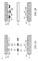
- FIGS. 2A to 2 D are four plan views sequentially depicting the steps for forming a laminated structure ( 2 ) according to the present invention.
- FIG. 3 is an enlarged view according to a dotted line (Z) of FIG. 2 D.
- FIGS. 2A to 2 D are four plan views sequentially depicting the steps for forming a laminated structure 2 according to the present invention.
- the laminated structure 2 comprises a first substrate 21 , a second substrate 22 , a plurality of particles 23 and an intermediate 24 , wherein the first substrate 21 and the second substrate 22 can be the two conductive plates of LSI (Large Scale Integrated Circuit), COG (Chip On Glass), FPC (Flexible Printed Circuit), PCB (Printed Circuit Board) or TAB (Tape Automatic Bonding), TCP (Tape Carrier Package).
- LSI Large Scale Integrated Circuit
- COG Chip On Glass
- FPC Flexible Printed Circuit
- PCB Printed Circuit Board
- TAB Tape Automatic Bonding
- TCP Tape Carrier Package
- the first substrate 21 has a surface 210 provided with bumps, and a first conjunction portion A 1 ′ and a second conjunction portion A 2 ′ are the two next to each other.
- the first conjunction portion A 1 ′ has an end surface A 01 ′ and the second conjunction portion A 2 ′ has an end surface A 02 ′.
- the second substrate 22 has a base surface 220 with bumps, and a third conjunction portion B 1 ′ and a fourth conjunction portion B 2 ′ are two of them which are next to each other.
- the third conjunction portion B 1 ′ and the fourth conjunction portion B 2 ′ partially made of same conductive material such as gold, provide a first hardness.
- the third conjunction portion B 1 ′ has an end surface B 01 ′ and the fourth conjunction portion B 2 ′ has an end surface B 02 ′.
- a height difference t 3 exists between the third conjunction portion B 1 ′ (end surface B 01 ′) and the fourth conjunction portion B 2 ′ (end surface B 02 ′) with reference to the base surface 220 of the second substrate 22 .
- the particles 23 made of conductive material such as Nickel are provided with a second hardness greater than the first hardness and formed in the shape of ball or cube.
- the particles 23 are coated on the end surface B 01 ′ and the end surface B 02 ′, and the intermediate 24 preferably made of rubber such as epoxy is used as an adhesive material disposed between the first substrate 21 and the second substrate 22 .
- FIG. 2C shows the first substrate 21 and the second substrate 22 being brought together through the application of a clamping force F.
- FIG. 2D shows the first substrate 21 and the second substrate 22 being combined by the intermediate 24 and electrically connected to each other via the particles 23 .
- the particles 23 located on the fourth conjunction portion B 2 ′ first contact the end surface A 02 ′ of the second conjunction portion A 2 ′. Then, the particles 23 , originally located on the end surface B 02 ′ of the fourth conjunction portion B 2 ′, begin to be embedded in the fourth conjunction portion B 2 ′ by the pressure applied by the second conjunction portion A 2 ′.
- the embedding process can be terminated when the particles 23 located on the end surface B 01 ′ of the third conjunction portion B 1 ′ uniformly contact the end surface A 01 ′ of the first conjunction portion A 1 ′.
- the laminated structure 2 is formed and the clamping force F can be removed of the first substrate 21 and the second substrate 22 when the intermediate 24 disposed between the first substrate 21 and the second substrate 22 is solidified.
- FIG. 3 is an enlarged view according to a dotted line Z of FIG. 2 D.
- the height difference t 3 between the third conjunction portion B 1 ′ (end surface B 01 ′) and the fourth conjunction portion B 2 ′ (end surface B 02 ′) with reference to the base surface 220 , can be completely compensated by the embedded particles 23 located on the fourth conjunction portion B 2 ′.
- the junction between the third conjunction portion B 1 ′ and the first conjunction portion A 1 ′ can be uniformly performed by the particles 23 located there.
Abstract
A first substrate, a second substrate, an intermediate and a plurality of particles form a laminated structure. The first substrate has a first conjunction portion and a second conjunction portion, and the second substrate has a third conjunction portion and a fourth conjunction portion which are characterized by a first hardness. The intermediate is disposed between the first substrate and the second substrate. The particles provided with a second hardness greater than the first hardness are coated on the third conjunction portion to contact the first conjunction portion and coated on the fourth conjunction portion to contact the second conjunction portion. A height difference with reference to the base surface of the second substrate exists between the end surface of the third conjunction portion and the end surface of the fourth conjunction portion. A height difference that exists between the fourth conjunction portion and the third conjunction portion can be compensated for by the particles embedded in the fourth conjunction portion. Thus the bridging of the third conjunction portion and the first conjunction portion can be uniformly performed by the particles located between the two.
Description
This application is a divisional application of U.S. application Ser. No. 09/920,370 filed on Aug. 1, 2001, which is hereby incorporated by reference in its entirety.
1. Field of the Invention
This invention relates to a laminated structure. More particularly, this invention relates to a laminated structure provided with pairs of corresponding bumps or conjunction portions which are electrically connected to each other by particles embedded.
2. Description of Prior Art
ACF (Anisotropic Conductive Film) is a conductive film composed of epoxy resin and a plurality of metal particles and is often used as interlayer clamped between two corresponding bumps or electrodes of a substrate and LSI (Large Scale Integrated Circuit), COG (Chip On Glass), FPC (Flexible Printed Circuit), PCB (Printed Circuit Board), TAB (Tape Automatic Bonding) or TCP (Tape Carrier Package) so as to form a laminated structure for use in LCD panels.
However, two adjacent bumps or electrodes of the substrate can easily short-circuit or suffer low conductivity when the laminated structure is bent, causing the particles in the ACF that are located between two electrodes, to crowd together.
Further, the manufacturing process of ACF is complicated, and the tolerance of the height difference among the bumps of LSI/FPC/PCB/TCP cannot always be precisely controlled. If the design aims to increase the amount of conductive particles captured by the bumps or electrodes, the size of the bumps or electrodes formed on the LSI/FPC/PCB/TCP cannot be too small to contact the conductive particles within the predetermined area. If the design aims to increase the conductivity between two corresponding bumps or electrodes by increasing the number of particles in the ACF, the effective space (Fine Pitch Design) between any two of the adjacent bumps or electrodes cannot be so narrow as to cause a short circuit.
FIGS. 1A, 1B and 1C are three plan views sequentially depicting the steps for forming a laminated structure 1 according to a prior art. The substrate 11, 12 are two conductive plates of LSI/COG/FPC/PCB/TAB/TCP.
As shown in FIG. 1A, the laminated structure 1 is composed of two substrates 11(12), a plurality of conductive particles 13 and an epoxy 14. The substrate 11 has a surface 110 with a plurality of spaced bumps A1˜A3, and the substrate 12 has a surface 120 with a plurality of spaced bumps (B1˜B3) corresponding to bumps A1˜A3. The so-called Anisotropic Conductive Film (ACF) is made of epoxy 14 mixed with the particles 13, and the ACF is used as an intermediate to bond the substrates 11 and the substrates 12 together and electrically connect the substrates 11 to the substrates 12. The bumps A1˜A3 of the substrate 11 are respectively provided with end surfaces A01, A02 and A03, and the bumps B1˜B3 of the substrate 12 are respectively provided with end surfaces B01, B02 and B03. A height difference t1 exists between the bump B1 and the bump B2, and another height difference t2 exists between bump B2 and bump B3.
FIG. 1B shows the substrate 11 and the substrate 12 being brought toward each other by the application of a clamping force F. FIG. 1C shows the first substrate 21 and the second substrate 22 being combined together by the epoxy 14 and electrically connected to each other via the particles 13.
In FIG. 1B, a force F is applied on the two substrates 11, 12 to form the laminated structure 1. The epoxy 14 is gradually deformed and thinned by the approaching substrates 11 and 12, and then the particles 13 stored in the epoxy 14 are irregularly dispersed during the clamping process. Then, the bump A1 and the bump B1, the bump A2 and the bump B2, the bump A3 and the bump B3 respectively clamp the particles 13 stored in the epoxy 14 as shown in FIG. 1C.
However, with the height differences t1 and t2 between bump B2 and bump B1, B2, the number of the particles 13 clamped between each two corresponding bumps is quite different, i.e. the particles 13 are not easily captured by the any two corresponding bumps. Moreover, a short circuit may occur between any two of the bumps of the substrate 11 or 12 between which the number of the particles 13 is dense.
U.S. Pat. No. 5,065,505 disclosed by Hiroshi Matsubara et al, Sharp Kabushiki Kaisha, mentions that the conductive particles are adhered to the electrodes of the glass board by means of the uncured photocuring adhesive. However, height differences existing among the electrodes cannot be effectively compensated while the circuit board is connected to the electrodes of the glass board.
The primary object of this invention is to provide a laminated structure, comprising a first substrate, a second substrate, an intermediate and a plurality of particles. The first substrate has a first conjunction portion and a second conjunction portion, and the second substrate has a third conjunction portion and a fourth conjunction portion which are provided with a first hardness. The intermediate is disposed between the first substrate and the second substrate. The particles with a second hardness larger than the first hardness are coated on the third conjunction portion for contacting the first conjunction portion and coated on the fourth conjunction portion for contacting the second conjunction portion. A height difference with reference to the base surface of the second substrate exists between the end surface of the third conjunction portion and the end surface of the fourth conjunction portion.
A height difference is exists between the fourth conjunction portion and the third conjunction portion and the height of the fourth conjunction portion is presupposed lower than that of the third conjunction portion. The height difference can be compensated by the particles embedded in the fourth conjunction portion when a clamping force is applied, and therefore the junction between the third conjunction portion and the first conjunction portion can be uniformly bridged by the particles located therebetween.
The present invention can be more fully understood by reading the subsequent detailed description and examples with reference made to accompanying drawings in which:
FIGS. 1A to 1C are three plan views sequentially depicting the steps for forming a laminated structure (1) according to a prior art;
FIGS. 2A to 2D are four plan views sequentially depicting the steps for forming a laminated structure (2) according to the present invention; and
FIG. 3 is an enlarged view according to a dotted line (Z) of FIG. 2D.
FIGS. 2A to 2D are four plan views sequentially depicting the steps for forming a laminated structure 2 according to the present invention.
In FIGS. 2A and 2B, the laminated structure 2 comprises a first substrate 21, a second substrate 22, a plurality of particles 23 and an intermediate 24, wherein the first substrate 21 and the second substrate 22 can be the two conductive plates of LSI (Large Scale Integrated Circuit), COG (Chip On Glass), FPC (Flexible Printed Circuit), PCB (Printed Circuit Board) or TAB (Tape Automatic Bonding), TCP (Tape Carrier Package).
The first substrate 21 has a surface 210 provided with bumps, and a first conjunction portion A1′ and a second conjunction portion A2′ are the two next to each other. The first conjunction portion A1′ has an end surface A01′ and the second conjunction portion A2′ has an end surface A02′. The second substrate 22 has a base surface 220 with bumps, and a third conjunction portion B1′ and a fourth conjunction portion B2′ are two of them which are next to each other. The third conjunction portion B1′ and the fourth conjunction portion B2′, partially made of same conductive material such as gold, provide a first hardness. The third conjunction portion B1′ has an end surface B01′ and the fourth conjunction portion B2′ has an end surface B02′.
A height difference t3 exists between the third conjunction portion B1′ (end surface B01′) and the fourth conjunction portion B2′ (end surface B02′) with reference to the base surface 220 of the second substrate 22. The particles 23 made of conductive material such as Nickel are provided with a second hardness greater than the first hardness and formed in the shape of ball or cube. In FIG. 2B, the particles 23 are coated on the end surface B01′ and the end surface B02′, and the intermediate 24 preferably made of rubber such as epoxy is used as an adhesive material disposed between the first substrate 21 and the second substrate 22.
FIG. 2C shows the first substrate 21 and the second substrate 22 being brought together through the application of a clamping force F. FIG. 2D shows the first substrate 21 and the second substrate 22 being combined by the intermediate 24 and electrically connected to each other via the particles 23.
With the force F disposed on the first substrate 21 and the second substrate 22, the particles 23 located on the fourth conjunction portion B2′ first contact the end surface A02′ of the second conjunction portion A2′. Then, the particles 23, originally located on the end surface B02′ of the fourth conjunction portion B2′, begin to be embedded in the fourth conjunction portion B2′ by the pressure applied by the second conjunction portion A2′. The embedding process can be terminated when the particles 23 located on the end surface B01′ of the third conjunction portion B1′ uniformly contact the end surface A01′ of the first conjunction portion A1′.
Then, the laminated structure 2 is formed and the clamping force F can be removed of the first substrate 21 and the second substrate 22 when the intermediate 24 disposed between the first substrate 21 and the second substrate 22 is solidified.
FIG. 3 is an enlarged view according to a dotted line Z of FIG. 2D. The height difference t3, between the third conjunction portion B1′ (end surface B01′) and the fourth conjunction portion B2′ (end surface B02′) with reference to the base surface 220, can be completely compensated by the embedded particles 23 located on the fourth conjunction portion B2′. The junction between the third conjunction portion B1′ and the first conjunction portion A1′ can be uniformly performed by the particles 23 located there.
While this invention has been described in connection with what is presently considered to be the most practical and preferred embodiment, it is to be understood that the invention is not limited to the disclosed embodiments, but, on the contrary, is intended to cover various modifications and equivalent arrangements included within the spirit and scope of the appended claims.
Claims (3)
1. A method for forming a laminated structure, comprising:
providing a first substrate and a second substrate, the first substrate having a first group of conjunction portions and the second substrate having a second group of conjunction portions, a height difference being between the conjunction portions within the second group; and
connecting the first substrate to the second substrate to electrically connect the first group conjunction portions and the second group conjunction portion with a plurality of particles, a part of the particles embedded in the second group conjunction portions to compensate the height difference therebetween.
2. A method for forming a laminated structure, comprising:
providing a first substrate and a second substrate, the first substrate having a first conjunction portion and a second conjunction portion and the second substrate having a third conjunction portion and a fourth conjunction portion, the fourth conjunction portion being higher than the third conjunction portion; and
connecting the first substrate to the second substrate with a plurality of particles and an intermediate, the particles between the second and fourth conjunction portions embedded in the fourth conjunction portion and the particles between the first and third conjunction portions uniformly bridged therebetween to compensate a height difference between the third conjunction portion and the fourth conjunction portion.
3. The method for forming a laminated structure as claimed in claim 2 , wherein the step of connecting the first substrate to the second substrate comprising:
applying the particles on the third conjunction portion and the fourth conjunction portion; and
applying the intermediate between the first substrate and the second substrate to electrically connect the third and first Conjunction portions and electrically connect the fourth and second conjunction portions through the particles.
Priority Applications (2)
| Application Number | Priority Date | Filing Date | Title |
|---|---|---|---|
| US10/057,605 US6802930B2 (en) | 2000-12-16 | 2002-01-24 | Method of making a laminated structure |
| US10/888,890 US20040244906A1 (en) | 2000-12-16 | 2004-07-08 | Laminated structure |
Applications Claiming Priority (5)
| Application Number | Priority Date | Filing Date | Title |
|---|---|---|---|
| TW089126964A TW554191B (en) | 2000-12-16 | 2000-12-16 | Laminating structure and its forming method |
| TW89126964 | 2000-12-16 | ||
| TW89126964A | 2000-12-16 | ||
| US09/920,370 US20020076537A1 (en) | 2000-12-16 | 2001-08-01 | Laminated structure |
| US10/057,605 US6802930B2 (en) | 2000-12-16 | 2002-01-24 | Method of making a laminated structure |
Related Parent Applications (1)
| Application Number | Title | Priority Date | Filing Date |
|---|---|---|---|
| US09/920,370 Division US20020076537A1 (en) | 2000-12-16 | 2001-08-01 | Laminated structure |
Related Child Applications (1)
| Application Number | Title | Priority Date | Filing Date |
|---|---|---|---|
| US10/888,890 Continuation US20040244906A1 (en) | 2000-12-16 | 2004-07-08 | Laminated structure |
Publications (2)
| Publication Number | Publication Date |
|---|---|
| US20020074385A1 US20020074385A1 (en) | 2002-06-20 |
| US6802930B2 true US6802930B2 (en) | 2004-10-12 |
Family
ID=21662352
Family Applications (3)
| Application Number | Title | Priority Date | Filing Date |
|---|---|---|---|
| US09/920,370 Abandoned US20020076537A1 (en) | 2000-12-16 | 2001-08-01 | Laminated structure |
| US10/057,605 Expired - Lifetime US6802930B2 (en) | 2000-12-16 | 2002-01-24 | Method of making a laminated structure |
| US10/888,890 Abandoned US20040244906A1 (en) | 2000-12-16 | 2004-07-08 | Laminated structure |
Family Applications Before (1)
| Application Number | Title | Priority Date | Filing Date |
|---|---|---|---|
| US09/920,370 Abandoned US20020076537A1 (en) | 2000-12-16 | 2001-08-01 | Laminated structure |
Family Applications After (1)
| Application Number | Title | Priority Date | Filing Date |
|---|---|---|---|
| US10/888,890 Abandoned US20040244906A1 (en) | 2000-12-16 | 2004-07-08 | Laminated structure |
Country Status (2)
| Country | Link |
|---|---|
| US (3) | US20020076537A1 (en) |
| TW (1) | TW554191B (en) |
Cited By (3)
| Publication number | Priority date | Publication date | Assignee | Title |
|---|---|---|---|---|
| US20050012225A1 (en) * | 2002-11-15 | 2005-01-20 | Choi Seung-Yong | Wafer-level chip scale package and method for fabricating and using the same |
| US20070238262A1 (en) * | 2006-03-28 | 2007-10-11 | Innovative Micro Technology | Wafer bonding material with embedded rigid particles |
| US20100155888A1 (en) * | 2008-12-24 | 2010-06-24 | International Business Machines Corporation | Silicon interposer testing for three dimensional chip stack |
Families Citing this family (9)
| Publication number | Priority date | Publication date | Assignee | Title |
|---|---|---|---|---|
| JP2002075064A (en) * | 2000-08-23 | 2002-03-15 | Tdk Corp | Anisotropic conductive film and its manufacturing method, and display using anisotropic conductive film |
| WO2003003798A1 (en) * | 2001-06-29 | 2003-01-09 | Toray Engineering Co., Ltd. | Joining method using anisotropic conductive adhesive |
| US6916398B2 (en) * | 2001-10-26 | 2005-07-12 | Applied Materials, Inc. | Gas delivery apparatus and method for atomic layer deposition |
| US8510935B2 (en) * | 2007-07-10 | 2013-08-20 | Joseph C Fjelstad | Electronic assemblies without solder and methods for their manufacture |
| WO2012073739A1 (en) * | 2010-11-29 | 2012-06-07 | シャープ株式会社 | Substrate module |
| WO2016114320A1 (en) * | 2015-01-13 | 2016-07-21 | デクセリアルズ株式会社 | Multilayer substrate |
| US10411218B2 (en) * | 2017-10-30 | 2019-09-10 | Wuhun China Star Optoelectronics Semiconductor Display Technology Co., Ltd. | Quasi crystalline conductive particles between a substrate and IC chip |
| CN112399037B (en) * | 2019-08-15 | 2022-04-05 | 宁波舜宇光电信息有限公司 | Photosensitive assembly, camera module and manufacturing method thereof |
| JP2021197519A (en) | 2020-06-17 | 2021-12-27 | 東北マイクロテック株式会社 | Laminated semiconductor device and mounting component, substrate, and bump connector used for laminated semiconductor device |
Citations (3)
| Publication number | Priority date | Publication date | Assignee | Title |
|---|---|---|---|---|
| US5065505A (en) | 1989-10-17 | 1991-11-19 | Sharp Kabushiki Kaisha | Method for connecting circuit boards |
| US5965064A (en) * | 1997-10-28 | 1999-10-12 | Sony Chemicals Corporation | Anisotropically electroconductive adhesive and adhesive film |
| US6137162A (en) * | 1998-05-12 | 2000-10-24 | Hyundai Electronics Industries Co., Ltd. | Chip stack package |
Family Cites Families (3)
| Publication number | Priority date | Publication date | Assignee | Title |
|---|---|---|---|---|
| JPH07307410A (en) * | 1994-05-16 | 1995-11-21 | Hitachi Ltd | Semiconductor device |
| JPH1084014A (en) * | 1996-07-19 | 1998-03-31 | Shinko Electric Ind Co Ltd | Manufacture of semiconductor device |
| JP3678547B2 (en) * | 1997-07-24 | 2005-08-03 | ソニーケミカル株式会社 | Multilayer anisotropic conductive adhesive and method for producing the same |
-
2000
- 2000-12-16 TW TW089126964A patent/TW554191B/en not_active IP Right Cessation
-
2001
- 2001-08-01 US US09/920,370 patent/US20020076537A1/en not_active Abandoned
-
2002
- 2002-01-24 US US10/057,605 patent/US6802930B2/en not_active Expired - Lifetime
-
2004
- 2004-07-08 US US10/888,890 patent/US20040244906A1/en not_active Abandoned
Patent Citations (3)
| Publication number | Priority date | Publication date | Assignee | Title |
|---|---|---|---|---|
| US5065505A (en) | 1989-10-17 | 1991-11-19 | Sharp Kabushiki Kaisha | Method for connecting circuit boards |
| US5965064A (en) * | 1997-10-28 | 1999-10-12 | Sony Chemicals Corporation | Anisotropically electroconductive adhesive and adhesive film |
| US6137162A (en) * | 1998-05-12 | 2000-10-24 | Hyundai Electronics Industries Co., Ltd. | Chip stack package |
Non-Patent Citations (1)
| Title |
|---|
| Flip Chip Technologies, by John Lau(editor), McGraw Hill, 1995, p. 326-331. * |
Cited By (5)
| Publication number | Priority date | Publication date | Assignee | Title |
|---|---|---|---|---|
| US20050012225A1 (en) * | 2002-11-15 | 2005-01-20 | Choi Seung-Yong | Wafer-level chip scale package and method for fabricating and using the same |
| US20070238262A1 (en) * | 2006-03-28 | 2007-10-11 | Innovative Micro Technology | Wafer bonding material with embedded rigid particles |
| US7807547B2 (en) | 2006-03-28 | 2010-10-05 | Innovative Micro Technology | Wafer bonding material with embedded rigid particles |
| US20100155888A1 (en) * | 2008-12-24 | 2010-06-24 | International Business Machines Corporation | Silicon interposer testing for three dimensional chip stack |
| US7863106B2 (en) * | 2008-12-24 | 2011-01-04 | International Business Machines Corporation | Silicon interposer testing for three dimensional chip stack |
Also Published As
| Publication number | Publication date |
|---|---|
| TW554191B (en) | 2003-09-21 |
| US20020074385A1 (en) | 2002-06-20 |
| US20040244906A1 (en) | 2004-12-09 |
| US20020076537A1 (en) | 2002-06-20 |
Similar Documents
| Publication | Publication Date | Title |
|---|---|---|
| EP0827632B1 (en) | Semiconductor device having a semiconductor chip electrically connected to a wiring substrate | |
| US6579744B1 (en) | Electrical interconnections, methods of conducting electricity, and methods of reducing horizontal conductivity within an anisotropic conductive adhesive | |
| US7208835B2 (en) | Integrated circuit package and assembly thereof | |
| US5903056A (en) | Conductive polymer film bonding technique | |
| JP4987880B2 (en) | Circuit board connection structure using anisotropic conductive film, adhesion method, and adhesion state evaluation method using the same | |
| US20010002330A1 (en) | Rolling ball connector | |
| US6802930B2 (en) | Method of making a laminated structure | |
| KR100563890B1 (en) | Electrical connecting device and electrical connecting method | |
| KR100248313B1 (en) | A tape carrier package with improved connecting terminals and a method of electrically interconnecting the tape carrier package to external circuit board | |
| EP0662256A1 (en) | An electrical connecting structure and a method for electrically connecting terminals to each other | |
| CN103140052A (en) | Electronic module | |
| JPH0927516A (en) | Connection structure of electronic component | |
| KR100701133B1 (en) | Electric connecting method and apparatus | |
| KR100635425B1 (en) | Structure and method for bonding an ic chip | |
| CN100416343C (en) | Structure for increasing reliability of metal connecting line | |
| JP3052300B2 (en) | Wiring board and pressure tool | |
| JP2004006417A (en) | Connecting element and connection structure of electrode using this | |
| JP3876993B2 (en) | Adhesive structure, liquid crystal device, and electronic device | |
| KR101008824B1 (en) | Semiconductor device having electrode attached polymer particle and Semiconductor package using the same | |
| US7312142B2 (en) | Method for making cable with a conductive bump array, and method for connecting the cable to a task object | |
| CN112740483A (en) | Anisotropic conductive film, connection structure, and method for producing connection structure | |
| KR100877264B1 (en) | Semiconductor device having electrode for low pressure bonding and Semiconductor package using the same | |
| TW201816029A (en) | Anisotropic conductive film | |
| JP2000208907A (en) | Mounting method for electronic component | |
| JPH08148212A (en) | Connection member and structure and method for connecting electrode using the same |
Legal Events
| Date | Code | Title | Description |
|---|---|---|---|
| STCF | Information on status: patent grant |
Free format text: PATENTED CASE |
|
| FPAY | Fee payment |
Year of fee payment: 4 |
|
| REMI | Maintenance fee reminder mailed | ||
| FPAY | Fee payment |
Year of fee payment: 8 |
|
| FPAY | Fee payment |
Year of fee payment: 12 |