US6807214B2 - Integrated laser and electro-absorption modulator with improved extinction - Google Patents
Integrated laser and electro-absorption modulator with improved extinction Download PDFInfo
- Publication number
- US6807214B2 US6807214B2 US10/211,865 US21186502A US6807214B2 US 6807214 B2 US6807214 B2 US 6807214B2 US 21186502 A US21186502 A US 21186502A US 6807214 B2 US6807214 B2 US 6807214B2
- Authority
- US
- United States
- Prior art keywords
- region
- modulator
- layer
- laser
- modulator region
- Prior art date
- Legal status (The legal status is an assumption and is not a legal conclusion. Google has not performed a legal analysis and makes no representation as to the accuracy of the status listed.)
- Expired - Fee Related
Links
Images

Classifications
-
- H—ELECTRICITY
- H01—ELECTRIC ELEMENTS
- H01S—DEVICES USING THE PROCESS OF LIGHT AMPLIFICATION BY STIMULATED EMISSION OF RADIATION [LASER] TO AMPLIFY OR GENERATE LIGHT; DEVICES USING STIMULATED EMISSION OF ELECTROMAGNETIC RADIATION IN WAVE RANGES OTHER THAN OPTICAL
- H01S5/00—Semiconductor lasers
- H01S5/02—Structural details or components not essential to laser action
- H01S5/026—Monolithically integrated components, e.g. waveguides, monitoring photo-detectors, drivers
- H01S5/0265—Intensity modulators
-
- B—PERFORMING OPERATIONS; TRANSPORTING
- B82—NANOTECHNOLOGY
- B82Y—SPECIFIC USES OR APPLICATIONS OF NANOSTRUCTURES; MEASUREMENT OR ANALYSIS OF NANOSTRUCTURES; MANUFACTURE OR TREATMENT OF NANOSTRUCTURES
- B82Y20/00—Nanooptics, e.g. quantum optics or photonic crystals
-
- H—ELECTRICITY
- H01—ELECTRIC ELEMENTS
- H01S—DEVICES USING THE PROCESS OF LIGHT AMPLIFICATION BY STIMULATED EMISSION OF RADIATION [LASER] TO AMPLIFY OR GENERATE LIGHT; DEVICES USING STIMULATED EMISSION OF ELECTROMAGNETIC RADIATION IN WAVE RANGES OTHER THAN OPTICAL
- H01S5/00—Semiconductor lasers
- H01S5/30—Structure or shape of the active region; Materials used for the active region
- H01S5/34—Structure or shape of the active region; Materials used for the active region comprising quantum well or superlattice structures, e.g. single quantum well [SQW] lasers, multiple quantum well [MQW] lasers or graded index separate confinement heterostructure [GRINSCH] lasers
- H01S5/3403—Structure or shape of the active region; Materials used for the active region comprising quantum well or superlattice structures, e.g. single quantum well [SQW] lasers, multiple quantum well [MQW] lasers or graded index separate confinement heterostructure [GRINSCH] lasers having a strained layer structure in which the strain performs a special function, e.g. general strain effects, strain versus polarisation
-
- H—ELECTRICITY
- H01—ELECTRIC ELEMENTS
- H01S—DEVICES USING THE PROCESS OF LIGHT AMPLIFICATION BY STIMULATED EMISSION OF RADIATION [LASER] TO AMPLIFY OR GENERATE LIGHT; DEVICES USING STIMULATED EMISSION OF ELECTROMAGNETIC RADIATION IN WAVE RANGES OTHER THAN OPTICAL
- H01S5/00—Semiconductor lasers
- H01S5/30—Structure or shape of the active region; Materials used for the active region
- H01S5/34—Structure or shape of the active region; Materials used for the active region comprising quantum well or superlattice structures, e.g. single quantum well [SQW] lasers, multiple quantum well [MQW] lasers or graded index separate confinement heterostructure [GRINSCH] lasers
- H01S5/343—Structure or shape of the active region; Materials used for the active region comprising quantum well or superlattice structures, e.g. single quantum well [SQW] lasers, multiple quantum well [MQW] lasers or graded index separate confinement heterostructure [GRINSCH] lasers in AIIIBV compounds, e.g. AlGaAs-laser, InP-based laser
- H01S5/34306—Structure or shape of the active region; Materials used for the active region comprising quantum well or superlattice structures, e.g. single quantum well [SQW] lasers, multiple quantum well [MQW] lasers or graded index separate confinement heterostructure [GRINSCH] lasers in AIIIBV compounds, e.g. AlGaAs-laser, InP-based laser emitting light at a wavelength longer than 1000nm, e.g. InP based 1300 and 1500nm lasers
-
- H—ELECTRICITY
- H01—ELECTRIC ELEMENTS
- H01S—DEVICES USING THE PROCESS OF LIGHT AMPLIFICATION BY STIMULATED EMISSION OF RADIATION [LASER] TO AMPLIFY OR GENERATE LIGHT; DEVICES USING STIMULATED EMISSION OF ELECTROMAGNETIC RADIATION IN WAVE RANGES OTHER THAN OPTICAL
- H01S5/00—Semiconductor lasers
- H01S5/30—Structure or shape of the active region; Materials used for the active region
- H01S5/34—Structure or shape of the active region; Materials used for the active region comprising quantum well or superlattice structures, e.g. single quantum well [SQW] lasers, multiple quantum well [MQW] lasers or graded index separate confinement heterostructure [GRINSCH] lasers
- H01S5/343—Structure or shape of the active region; Materials used for the active region comprising quantum well or superlattice structures, e.g. single quantum well [SQW] lasers, multiple quantum well [MQW] lasers or graded index separate confinement heterostructure [GRINSCH] lasers in AIIIBV compounds, e.g. AlGaAs-laser, InP-based laser
- H01S5/34346—Structure or shape of the active region; Materials used for the active region comprising quantum well or superlattice structures, e.g. single quantum well [SQW] lasers, multiple quantum well [MQW] lasers or graded index separate confinement heterostructure [GRINSCH] lasers in AIIIBV compounds, e.g. AlGaAs-laser, InP-based laser characterised by the materials of the barrier layers
- H01S5/34373—Structure or shape of the active region; Materials used for the active region comprising quantum well or superlattice structures, e.g. single quantum well [SQW] lasers, multiple quantum well [MQW] lasers or graded index separate confinement heterostructure [GRINSCH] lasers in AIIIBV compounds, e.g. AlGaAs-laser, InP-based laser characterised by the materials of the barrier layers based on InGa(Al)AsP
Definitions
- the present invention relates to semiconductor lasers, and more particularly, to lasers that are coupled to light modulators.
- the light source is typically a laser.
- the modulation can be imparted to the light source by turning the laser on and off.
- this type of laser modulation leads to increased line width in the laser light. At frequencies at or above approximately 10 Ghz, this increased line width cannot be tolerated.
- light sources that are to be modulated at frequencies above 10 GHz are typically constructed by providing a laser that runs continuously and a separate light modulator that modulates the intensity of the laser output.
- the modulator typically has a transmissive state and an opaque state, which are switched back and forth by applying a potential across the modulator.
- the laser and modulator are constructed on a common substrate.
- the length of the modulator section is preferably as short as possible to maximize the performance of the modulator. However, the length of the modulator must be sufficient to provide the desired contrast between the transmissive and opaque states of the modulator.
- the present invention is a modulated light emitter having a laser and modulator constructed on a common substrate.
- the light emitter includes a first contact layer of a first semiconductor type and a first cladding layer on the contact layer of the first semiconductor type.
- An active layer is constructed on the cladding layer.
- the active layer includes a quantum well (QW) layer sandwiched between first and second barrier layers.
- QW quantum well
- a second cladding layer of the opposite semiconductor type and a second contact layer of the opposite semiconductor type are constructed over the active layer.
- the active layer includes a laser region and a modulator region connected by a waveguide. The laser region emits light when a potential is applied across the active layer in the laser region.
- the modulator region has a first state in which the modulator region absorbs the generated light and a second state in which the modulator region transmits the generated light.
- the modulator region assumes either the first or second state depending on the potential across the modulator region.
- the QW layer in the modulator region is under a tensile strain, which provides improved light absorption in the first state.
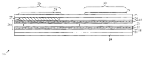
- FIG. 1 is a cross-sectional view through a modulated light source 10 consisting of a laser 20 and a modulator 30 .
- FIG. 1 is a cross-sectional view through a modulated light source 10 consisting of a laser 20 and a modulator 30 . Both the laser and modulator are constructed by depositing a number of layers on a suitable substrate that has been omitted from the drawing.
- the bottom layers typically include an n-type contact layer 19 and a cladding layer 21 .
- An active region 26 is grown on top of cladding layer 21
- Layer 26 includes one or more strained quantum well layers 22 separated by barrier layers 23 .
- a confinement layer 18 is typically deposited on each side of the active region.
- a p-type cladding layer 24 and a p-type contact layer 25 are deposited on the active region.
- a distributed Bragg reflector 27 sets the wavelength of the laser light in the embodiment shown in FIG. 1 .
- Electrodes 28 and 29 are then deposited on contact layer 25 .
- Laser 20 is powered by providing a potential difference between electrode 28 and contact layer 19 .
- Modulator 30 is switched between a transparent and opaque state by modulating the potential difference between electrode 29 and contact layer 19 .
- the common electrode used to make contact with contact layer 19 has been omitted from the drawing.
- Modulator 30 is based on the observation that the quantum well structures will absorb light below a cutoff wavelength whose value depends on the potential across the quantum well layers.
- the position of the cutoff wavelength is determined by the composition of the quantum well layers. To provide the desired switching function, this cutoff wavelength must move from a value below the wavelength of the laser light generated by laser 20 to a value above the laser wavelength when the potential across the modulator layers is switched.
- the quantum wells are typically constructed from In x Ga 1 ⁇ x As y P 1 ⁇ y .
- the relative amount of In and Ga determine the bandgaps of the quantum wells, and hence, the location of the cutoff and the wavelength of the laser light.
- Higher In concentrations i.e., greater x values
- higher Ga concentrations increase the bandgap.
- a technique known as “selective-area growth” is typically used to shift the bandgap of InGaAsP layers across the device. This technique is based on the observation that indium does not deposit on SiO 2 . Hence, if the area that is to have an increased In concentration is bounded by SiO 2 masks, some of the indium that would have been deposited on the mask area moves into the area between the masks and increases the concentration of indium in that region.
- the base wavelength of the InGaAsP quantum well (QW) active region is adjusted to about 1480 nm.
- the indium content and growth rate of InGaAsP QWs is selectively enhanced, resulting in a local wavelength shift to 1550 nm.
- a laser is fabricated from the selectively-grown 1550 nm QW material, while a modulator is fabricated from the 1480 nm material.
- the two devices lie along a common waveguide, defined by either a buried heterostructure or ridge waveguide. To simplify the drawings, the waveguide has been omitted.
- the maximum attenuation of the modulator in the opaque state depends on the length of the modulator section.
- a high extinction ratio may be achieved by increasing absorption through longer modulators, more quantum wells, or operation with large voltage swings.
- these approaches also compromise the modulation rate.
- longer modulators translate into greater capacitance, and adding more QWs increases the carrier extraction time. Consequently, it is desirable to maximize the QW absorption without increasing the number of QW layers, so that the modulator can be made as short as possible.
- a layer is said to be compressively-strained if the “in-plane” lattice constant of that layer (i.e. the lattice constant within the plane of the substrate surface) is less than the lattice constant of the material in bulk.
- a layer is said to be under tensile strain if the in-plane lattice constant in that layer is greater than the lattice constant of the material in bulk. The strain arises when a layer is deposited on a substrate that has a different bulk lattice constant than that of the layer being deposited.
- the lattice constant of the layer within the plane of the substrate surface is forced to match that of the underlying layer, and hence, the layer is subjected to a stress.
- the degree of stress is normally specified by specifying the change in the lattice constant.
- a layer that is under a 1% compressive strain has an in-plane lattice constant that is 1% smaller than the material would exhibit in the bulk state.
- the present invention is based on the observation that the extinction ratio in the modulator section would be enhanced by approximately a factor of two if the QWs in that region were in a state of very slight tensile strain rather than the compressive strain utilized in prior art devices.
- the optimum tension depends on the thickness of the QW; however, a tension in the range of a few tenths of a percent has been found to be adequate. If the correct amount of tension is applied, the light-hole and heavy-hole valence band edges become degenerate in the modulator region. In this situation, the valence band density of states becomes extremely large, leading to a similarly large enhancement in the direct bandgap absorption or emission. Accordingly, by employing this effect, absorption in a QW modulator may be increased, and the modulator may therefore be made shorter to achieve a given extinction ratio. The reduction in modulator length, in turn, leads to lower capacitance and higher modulator speed.
- the level of strain in the QW layers depends on the ratio of In to Ga in the QW layers.
- the present invention is based on the observation that higher ratios of In to Ga shift the strain in the QW layer to be more compressive.
- the In/Ga ratio in the modulator region is set such that the modulator QW layer is under a small tensile strain, the increased In in the laser region will result in that region having less tensile strain or a compressive strain.
- the barrier layers that are grown between the QW layers need not be grown with the same strain characteristics as the QW layers. By providing barrier layers that are less strained than the QW layers, the overall strain within the device may be reduced.
- a laser/modulator device can be constructed from QW layers of In 0.45 Ga 0.55 As that are 8 nm thick separated by 8 nm barrier layers of In 0.91 Ga 0.09 As 0.39 P 0.61 in the modulator region.
- the SiO 2 masks in the laser section are adjusted in size to provide 10 nm QW layers of In 0.49 Ga 0.51 As in the laser region that are separated by 10 nm barrier layers of In 0.95 Ga 0.05 As 0.39 P 0.61 .
- This arrangement provides a tensile strain of 0.57% in the modulator QW layers and a tensile strain of 0.3% in the laser QW layers.
- the barrier layers are compressively strained in the two regions.
- the barrier layers in the modulator region are under a 0.6% compressive strain, and those in the laser region are under a 0.9% compressive strain.
- This exemplary laser/modulator provides light at a wavelength of approximately 1550 nm.
- a typical prior art laser/modulator for this wavelength utilizes QW layers whose compositions are adjusted to provide a 1% compressive strain in the laser region and a 0.7% compressive strain in the modulator region.
- the present invention has utilized a particular material system.
- the present invention may be practiced with any material system in which a slight tensile strain can be incorporated.
- laser/modulators based on AlGaInAs/InP, AlGaInP/GaAs, GaInAsSb/GaSb, or InGaAsNSb/GaAs can also be constructed utilizing the present invention.
Abstract
Description
Claims (7)
Priority Applications (2)
| Application Number | Priority Date | Filing Date | Title |
|---|---|---|---|
| US10/211,865 US6807214B2 (en) | 2002-08-01 | 2002-08-01 | Integrated laser and electro-absorption modulator with improved extinction |
| EP03010143A EP1387450A3 (en) | 2002-08-01 | 2003-05-05 | Integrated laser and electro-absorption modulator |
Applications Claiming Priority (1)
| Application Number | Priority Date | Filing Date | Title |
|---|---|---|---|
| US10/211,865 US6807214B2 (en) | 2002-08-01 | 2002-08-01 | Integrated laser and electro-absorption modulator with improved extinction |
Publications (2)
| Publication Number | Publication Date |
|---|---|
| US20040022289A1 US20040022289A1 (en) | 2004-02-05 |
| US6807214B2 true US6807214B2 (en) | 2004-10-19 |
Family
ID=30115259
Family Applications (1)
| Application Number | Title | Priority Date | Filing Date |
|---|---|---|---|
| US10/211,865 Expired - Fee Related US6807214B2 (en) | 2002-08-01 | 2002-08-01 | Integrated laser and electro-absorption modulator with improved extinction |
Country Status (2)
| Country | Link |
|---|---|
| US (1) | US6807214B2 (en) |
| EP (1) | EP1387450A3 (en) |
Cited By (4)
| Publication number | Priority date | Publication date | Assignee | Title |
|---|---|---|---|---|
| US20060279828A1 (en) * | 2005-06-08 | 2006-12-14 | Bour David P | Deep quantum well electro-absorption modulator |
| US20100003035A1 (en) * | 2006-07-28 | 2010-01-07 | Electronics And Telecommunications Research Institute | Laser diode having an abrupt turn-on, optical transmitter device using the same laser diode and optical communication apparatus |
| US20100008392A1 (en) * | 2008-07-11 | 2010-01-14 | Sumitomo Electric Industries, Ltd. | Semiconductor optical device |
| US20100213467A1 (en) * | 2007-08-16 | 2010-08-26 | The Trustees Of Columbia University In The City Of New York | Direct bandgap substrates and methods of making and using |
Citations (9)
| Publication number | Priority date | Publication date | Assignee | Title |
|---|---|---|---|---|
| US5363392A (en) * | 1991-11-18 | 1994-11-08 | The Furokawa Electric Co., Ltd. | Strained quantum well type semiconductor laser device |
| US5383211A (en) * | 1993-11-02 | 1995-01-17 | Xerox Corporation | TM-polarized laser emitter using III-V alloy with nitrogen |
| US5539763A (en) * | 1993-09-22 | 1996-07-23 | Mitsubishi Denki Kabushiki Kaisha | Semiconductor lasers and methods for fabricating semiconductor lasers |
| US5574289A (en) * | 1992-02-28 | 1996-11-12 | Hitachi, Ltd. | Semiconductor optical integrated device and light receiver using said device |
| US5889294A (en) * | 1996-02-27 | 1999-03-30 | Oki Electric Industry Co., Ltd. | Edge emitting LED having a selective-area growth optical absorption region |
| US6233264B1 (en) * | 1996-08-27 | 2001-05-15 | Ricoh Company, Ltd. | Optical semiconductor device having an active layer containing N |
| US6330263B1 (en) * | 1998-05-06 | 2001-12-11 | Sarnoff Corporation | Laser diode having separated, highly-strained quantum wells |
| US6339607B1 (en) * | 1999-10-29 | 2002-01-15 | E2O Communications, Inc. | Method and apparatus for modulated integrated optically pumped vertical cavity surface emitting lasers |
| US6455338B1 (en) * | 1999-03-29 | 2002-09-24 | Mitsubishi Denki Kabushiki Kaisha | Method of manufacturing an integrated semiconductor laser-modulator device |
Family Cites Families (4)
| Publication number | Priority date | Publication date | Assignee | Title |
|---|---|---|---|---|
| US5438584A (en) * | 1992-09-22 | 1995-08-01 | Xerox Corporation | Dual polarization laser diode with quaternary material system |
| JP2937148B2 (en) * | 1996-11-06 | 1999-08-23 | 日本電気株式会社 | Semiconductor integrated polarization mode converter |
| US7120183B2 (en) * | 2001-07-11 | 2006-10-10 | Optium Corporation | Electro-absorption modulated laser with high operating temperature tolerance |
| JP3904947B2 (en) * | 2002-03-01 | 2007-04-11 | 三菱電機株式会社 | Light modulator |
-
2002
- 2002-08-01 US US10/211,865 patent/US6807214B2/en not_active Expired - Fee Related
-
2003
- 2003-05-05 EP EP03010143A patent/EP1387450A3/en not_active Ceased
Patent Citations (9)
| Publication number | Priority date | Publication date | Assignee | Title |
|---|---|---|---|---|
| US5363392A (en) * | 1991-11-18 | 1994-11-08 | The Furokawa Electric Co., Ltd. | Strained quantum well type semiconductor laser device |
| US5574289A (en) * | 1992-02-28 | 1996-11-12 | Hitachi, Ltd. | Semiconductor optical integrated device and light receiver using said device |
| US5539763A (en) * | 1993-09-22 | 1996-07-23 | Mitsubishi Denki Kabushiki Kaisha | Semiconductor lasers and methods for fabricating semiconductor lasers |
| US5383211A (en) * | 1993-11-02 | 1995-01-17 | Xerox Corporation | TM-polarized laser emitter using III-V alloy with nitrogen |
| US5889294A (en) * | 1996-02-27 | 1999-03-30 | Oki Electric Industry Co., Ltd. | Edge emitting LED having a selective-area growth optical absorption region |
| US6233264B1 (en) * | 1996-08-27 | 2001-05-15 | Ricoh Company, Ltd. | Optical semiconductor device having an active layer containing N |
| US6330263B1 (en) * | 1998-05-06 | 2001-12-11 | Sarnoff Corporation | Laser diode having separated, highly-strained quantum wells |
| US6455338B1 (en) * | 1999-03-29 | 2002-09-24 | Mitsubishi Denki Kabushiki Kaisha | Method of manufacturing an integrated semiconductor laser-modulator device |
| US6339607B1 (en) * | 1999-10-29 | 2002-01-15 | E2O Communications, Inc. | Method and apparatus for modulated integrated optically pumped vertical cavity surface emitting lasers |
Cited By (8)
| Publication number | Priority date | Publication date | Assignee | Title |
|---|---|---|---|---|
| US20060279828A1 (en) * | 2005-06-08 | 2006-12-14 | Bour David P | Deep quantum well electro-absorption modulator |
| US20100003035A1 (en) * | 2006-07-28 | 2010-01-07 | Electronics And Telecommunications Research Institute | Laser diode having an abrupt turn-on, optical transmitter device using the same laser diode and optical communication apparatus |
| US20100213467A1 (en) * | 2007-08-16 | 2010-08-26 | The Trustees Of Columbia University In The City Of New York | Direct bandgap substrates and methods of making and using |
| US8441018B2 (en) * | 2007-08-16 | 2013-05-14 | The Trustees Of Columbia University In The City Of New York | Direct bandgap substrates and methods of making and using |
| US9257606B2 (en) | 2007-08-16 | 2016-02-09 | The Trustees Of Columbia University In The City Of New York | Direct bandgap substrates and methods of making and using |
| US9666600B2 (en) | 2007-08-16 | 2017-05-30 | The Trustees Of Columbia University In The City Of New York | Direct bandgap substrates and methods of making and using |
| US20100008392A1 (en) * | 2008-07-11 | 2010-01-14 | Sumitomo Electric Industries, Ltd. | Semiconductor optical device |
| US7957442B2 (en) * | 2008-07-11 | 2011-06-07 | Sumitomo Electric Industries, Ltd. | Semiconductor optical device |
Also Published As
| Publication number | Publication date |
|---|---|
| EP1387450A3 (en) | 2005-04-20 |
| US20040022289A1 (en) | 2004-02-05 |
| EP1387450A2 (en) | 2004-02-04 |
Similar Documents
| Publication | Publication Date | Title |
|---|---|---|
| US5048036A (en) | Heterostructure laser with lattice mismatch | |
| EP0645858B1 (en) | Strained quantum well structure having variable polarization dependence and optical device inducing the strained quantum well structure | |
| US4815087A (en) | High speed stable light emitting semiconductor device with low threshold current | |
| US6100543A (en) | Electro-absorption type semiconductor optical modulator having a quantum well structure | |
| JPH07202260A (en) | Distortion superlattice light emitting element | |
| GB2285172A (en) | Semiconductor laser device | |
| US5530580A (en) | Electro absorption optical modulators | |
| JPH0143472B2 (en) | ||
| US7889773B2 (en) | Semiconductor device | |
| JP3141080B2 (en) | Semiconductor functional element | |
| US6768137B2 (en) | Laminated semiconductor substrate and optical semiconductor element | |
| EP0614253B1 (en) | Multi-quantum well (MQW) structure laser diode/modulator integrated light source | |
| US4847573A (en) | Optical modulator | |
| JPH04218994A (en) | Semiconductor light emitting device | |
| US6807214B2 (en) | Integrated laser and electro-absorption modulator with improved extinction | |
| JP2003506877A (en) | Semiconductor structure using group III nitride quaternary material system | |
| JPH03263388A (en) | Optical semiconductor element and manufacture thereof | |
| KR20010070459A (en) | Dopant diffusion barrier layer for use in III-V structures | |
| US5579331A (en) | Delta-strained quantum-well semiconductor lasers and optical amplifiers | |
| JPH05275746A (en) | Tunable light-emitting diode | |
| US5362974A (en) | Group II-VI material semiconductor optical device with strained multiquantum barriers | |
| Bhattacharya et al. | Quantum well optical devices and materials | |
| US6574027B2 (en) | Optical modulator, and optical-modulator-intergrated laser diode | |
| JPH03231220A (en) | Optical semiconductor device | |
| JP4103490B2 (en) | Light modulator |
Legal Events
| Date | Code | Title | Description |
|---|---|---|---|
| AS | Assignment |
Owner name: AGILENT TECHNOLOGIES, INC., COLORADO Free format text: ASSIGNMENT OF ASSIGNORS INTEREST;ASSIGNORS:CORZINE, SCOTT W.;BOUR, DAVID P.;REEL/FRAME:013391/0678 Effective date: 20020729 |
|
| AS | Assignment |
Owner name: AVAGO TECHNOLOGIES GENERAL IP PTE. LTD., SINGAPORE Free format text: ASSIGNMENT OF ASSIGNORS INTEREST;ASSIGNOR:AGILENT TECHNOLOGIES, INC.;REEL/FRAME:017207/0020 Effective date: 20051201 |
|
| AS | Assignment |
Owner name: AVAGO TECHNOLOGIES FIBER IP (SINGAPORE) PTE. LTD., Free format text: ASSIGNMENT OF ASSIGNORS INTEREST;ASSIGNOR:AVAGO TECHNOLOGIES GENERAL IP (SINGAPORE) PTE. LTD.;REEL/FRAME:017675/0199 Effective date: 20060127 |
|
| FPAY | Fee payment |
Year of fee payment: 4 |
|
| FPAY | Fee payment |
Year of fee payment: 8 |
|
| AS | Assignment |
Owner name: AVAGO TECHNOLOGIES GENERAL IP (SINGAPORE) PTE. LTD Free format text: MERGER;ASSIGNOR:AVAGO TECHNOLOGIES FIBER IP (SINGAPORE) PTE. LTD.;REEL/FRAME:030369/0672 Effective date: 20121030 |
|
| AS | Assignment |
Owner name: AVAGO TECHNOLOGIES GENERAL IP (SINGAPORE) PTE. LTD Free format text: CORRECTIVE ASSIGNMENT TO CORRECT THE NAME OF THE ASSIGNEE PREVIOUSLY RECORDED ON REEL 017207 FRAME 0020. ASSIGNOR(S) HEREBY CONFIRMS THE ASSIGNMENT;ASSIGNOR:AGILENT TECHNOLOGIES, INC.;REEL/FRAME:038633/0001 Effective date: 20051201 |
|
| REMI | Maintenance fee reminder mailed | ||
| LAPS | Lapse for failure to pay maintenance fees | ||
| STCH | Information on status: patent discontinuation |
Free format text: PATENT EXPIRED DUE TO NONPAYMENT OF MAINTENANCE FEES UNDER 37 CFR 1.362 |
|
| FP | Lapsed due to failure to pay maintenance fee |
Effective date: 20161019 |