US6830701B2 - Method for fabricating microelectromechanical structures for liquid emission devices - Google Patents
Method for fabricating microelectromechanical structures for liquid emission devices Download PDFInfo
- Publication number
- US6830701B2 US6830701B2 US10/191,506 US19150602A US6830701B2 US 6830701 B2 US6830701 B2 US 6830701B2 US 19150602 A US19150602 A US 19150602A US 6830701 B2 US6830701 B2 US 6830701B2
- Authority
- US
- United States
- Prior art keywords
- layer
- sacrificial material
- electrode layer
- electrode
- patterned
- Prior art date
- Legal status (The legal status is an assumption and is not a legal conclusion. Google has not performed a legal analysis and makes no representation as to the accuracy of the status listed.)
- Expired - Fee Related, expires
Links
- 239000007788 liquid Substances 0.000 title claims description 31
- 238000000034 method Methods 0.000 title claims description 8
- 239000000463 material Substances 0.000 claims abstract description 34
- 238000000151 deposition Methods 0.000 claims abstract description 16
- 239000000758 substrate Substances 0.000 claims description 13
- 238000000059 patterning Methods 0.000 claims description 12
- 230000008021 deposition Effects 0.000 claims description 11
- 238000005530 etching Methods 0.000 claims description 9
- 238000004519 manufacturing process Methods 0.000 claims description 3
- 238000005498 polishing Methods 0.000 claims description 3
- 239000000126 substance Substances 0.000 claims description 3
- 239000010410 layer Substances 0.000 description 75
- 239000012530 fluid Substances 0.000 description 16
- 239000000976 ink Substances 0.000 description 14
- VYPSYNLAJGMNEJ-UHFFFAOYSA-N Silicium dioxide Chemical compound O=[Si]=O VYPSYNLAJGMNEJ-UHFFFAOYSA-N 0.000 description 10
- 229910021420 polycrystalline silicon Inorganic materials 0.000 description 7
- 229920005591 polysilicon Polymers 0.000 description 7
- 238000004518 low pressure chemical vapour deposition Methods 0.000 description 6
- 238000002161 passivation Methods 0.000 description 6
- 238000000926 separation method Methods 0.000 description 6
- 230000007246 mechanism Effects 0.000 description 5
- 235000012239 silicon dioxide Nutrition 0.000 description 5
- 239000000377 silicon dioxide Substances 0.000 description 5
- 229910052581 Si3N4 Inorganic materials 0.000 description 4
- 239000012528 membrane Substances 0.000 description 4
- 150000004767 nitrides Chemical class 0.000 description 4
- HQVNEWCFYHHQES-UHFFFAOYSA-N silicon nitride Chemical compound N12[Si]34N5[Si]62N3[Si]51N64 HQVNEWCFYHHQES-UHFFFAOYSA-N 0.000 description 4
- 239000004642 Polyimide Substances 0.000 description 3
- 239000004020 conductor Substances 0.000 description 3
- 230000009977 dual effect Effects 0.000 description 3
- 239000011521 glass Substances 0.000 description 3
- 238000000623 plasma-assisted chemical vapour deposition Methods 0.000 description 3
- 229920001721 polyimide Polymers 0.000 description 3
- XUIMIQQOPSSXEZ-UHFFFAOYSA-N Silicon Chemical compound [Si] XUIMIQQOPSSXEZ-UHFFFAOYSA-N 0.000 description 2
- 230000005684 electric field Effects 0.000 description 2
- 230000002093 peripheral effect Effects 0.000 description 2
- 238000005381 potential energy Methods 0.000 description 2
- 229910052710 silicon Inorganic materials 0.000 description 2
- 239000010703 silicon Substances 0.000 description 2
- 244000208734 Pisonia aculeata Species 0.000 description 1
- QVGXLLKOCUKJST-UHFFFAOYSA-N atomic oxygen Chemical compound [O] QVGXLLKOCUKJST-UHFFFAOYSA-N 0.000 description 1
- 230000015556 catabolic process Effects 0.000 description 1
- 238000007654 immersion Methods 0.000 description 1
- 238000007641 inkjet printing Methods 0.000 description 1
- 229910021421 monocrystalline silicon Inorganic materials 0.000 description 1
- 229910052760 oxygen Inorganic materials 0.000 description 1
- 239000001301 oxygen Substances 0.000 description 1
- 238000000206 photolithography Methods 0.000 description 1
- 238000007639 printing Methods 0.000 description 1
- 239000002356 single layer Substances 0.000 description 1
Images


Classifications
-
- B—PERFORMING OPERATIONS; TRANSPORTING
- B41—PRINTING; LINING MACHINES; TYPEWRITERS; STAMPS
- B41J—TYPEWRITERS; SELECTIVE PRINTING MECHANISMS, i.e. MECHANISMS PRINTING OTHERWISE THAN FROM A FORME; CORRECTION OF TYPOGRAPHICAL ERRORS
- B41J2/00—Typewriters or selective printing mechanisms characterised by the printing or marking process for which they are designed
- B41J2/005—Typewriters or selective printing mechanisms characterised by the printing or marking process for which they are designed characterised by bringing liquid or particles selectively into contact with a printing material
- B41J2/01—Ink jet
- B41J2/135—Nozzles
- B41J2/16—Production of nozzles
- B41J2/1621—Manufacturing processes
- B41J2/1626—Manufacturing processes etching
-
- B—PERFORMING OPERATIONS; TRANSPORTING
- B41—PRINTING; LINING MACHINES; TYPEWRITERS; STAMPS
- B41J—TYPEWRITERS; SELECTIVE PRINTING MECHANISMS, i.e. MECHANISMS PRINTING OTHERWISE THAN FROM A FORME; CORRECTION OF TYPOGRAPHICAL ERRORS
- B41J2/00—Typewriters or selective printing mechanisms characterised by the printing or marking process for which they are designed
- B41J2/005—Typewriters or selective printing mechanisms characterised by the printing or marking process for which they are designed characterised by bringing liquid or particles selectively into contact with a printing material
- B41J2/01—Ink jet
- B41J2/135—Nozzles
- B41J2/16—Production of nozzles
- B41J2/1621—Manufacturing processes
- B41J2/1631—Manufacturing processes photolithography
-
- B—PERFORMING OPERATIONS; TRANSPORTING
- B41—PRINTING; LINING MACHINES; TYPEWRITERS; STAMPS
- B41J—TYPEWRITERS; SELECTIVE PRINTING MECHANISMS, i.e. MECHANISMS PRINTING OTHERWISE THAN FROM A FORME; CORRECTION OF TYPOGRAPHICAL ERRORS
- B41J2/00—Typewriters or selective printing mechanisms characterised by the printing or marking process for which they are designed
- B41J2/005—Typewriters or selective printing mechanisms characterised by the printing or marking process for which they are designed characterised by bringing liquid or particles selectively into contact with a printing material
- B41J2/01—Ink jet
- B41J2/135—Nozzles
- B41J2/16—Production of nozzles
- B41J2/1621—Manufacturing processes
- B41J2/1632—Manufacturing processes machining
-
- B—PERFORMING OPERATIONS; TRANSPORTING
- B41—PRINTING; LINING MACHINES; TYPEWRITERS; STAMPS
- B41J—TYPEWRITERS; SELECTIVE PRINTING MECHANISMS, i.e. MECHANISMS PRINTING OTHERWISE THAN FROM A FORME; CORRECTION OF TYPOGRAPHICAL ERRORS
- B41J2/00—Typewriters or selective printing mechanisms characterised by the printing or marking process for which they are designed
- B41J2/005—Typewriters or selective printing mechanisms characterised by the printing or marking process for which they are designed characterised by bringing liquid or particles selectively into contact with a printing material
- B41J2/01—Ink jet
- B41J2/135—Nozzles
- B41J2/16—Production of nozzles
- B41J2/1621—Manufacturing processes
- B41J2/1637—Manufacturing processes molding
- B41J2/1639—Manufacturing processes molding sacrificial molding
-
- B—PERFORMING OPERATIONS; TRANSPORTING
- B41—PRINTING; LINING MACHINES; TYPEWRITERS; STAMPS
- B41J—TYPEWRITERS; SELECTIVE PRINTING MECHANISMS, i.e. MECHANISMS PRINTING OTHERWISE THAN FROM A FORME; CORRECTION OF TYPOGRAPHICAL ERRORS
- B41J2/00—Typewriters or selective printing mechanisms characterised by the printing or marking process for which they are designed
- B41J2/005—Typewriters or selective printing mechanisms characterised by the printing or marking process for which they are designed characterised by bringing liquid or particles selectively into contact with a printing material
- B41J2/01—Ink jet
- B41J2/135—Nozzles
- B41J2/16—Production of nozzles
- B41J2/1621—Manufacturing processes
- B41J2/164—Manufacturing processes thin film formation
- B41J2/1642—Manufacturing processes thin film formation thin film formation by CVD [chemical vapor deposition]
-
- B—PERFORMING OPERATIONS; TRANSPORTING
- B41—PRINTING; LINING MACHINES; TYPEWRITERS; STAMPS
- B41J—TYPEWRITERS; SELECTIVE PRINTING MECHANISMS, i.e. MECHANISMS PRINTING OTHERWISE THAN FROM A FORME; CORRECTION OF TYPOGRAPHICAL ERRORS
- B41J2/00—Typewriters or selective printing mechanisms characterised by the printing or marking process for which they are designed
- B41J2/005—Typewriters or selective printing mechanisms characterised by the printing or marking process for which they are designed characterised by bringing liquid or particles selectively into contact with a printing material
- B41J2/01—Ink jet
- B41J2/015—Ink jet characterised by the jet generation process
- B41J2/04—Ink jet characterised by the jet generation process generating single droplets or particles on demand
- B41J2002/043—Electrostatic transducer
Definitions
- the present invention relates generally to microelectromechanical (MEM) devices.
- the invention is thought to be advantageous when producing drop-on-demand liquid emission devices such as, for example, ink jet printers, and more particularly such devices which employ an electrostatic actuator for driving liquid from the device.
- DOD liquid emission devices with electrostatic actuators are known for ink printing systems.
- U.S. Pat. Nos. 5,644,341 and 5,668,579 which issued to Fujii et al. on Jul. 1, 1997 and Sep. 16, 1997, respectively, disclose such devices having electrostatic actuators composed of a diaphragm and opposed electrode. The diaphragm is distorted by application of a first voltage to the electrode. Relaxation of the diaphragm expels an ink droplet from the device.
- Other devices that operate on the principle of electrostatic attraction are disclosed in U.S. Pat. Nos. 5,739,831, 6,127,198, and 6,318,841; and in U.S. Publication No. 2001/0023523.
- U.S. Pat. No. 6,345,884 teaches a device having an electrostatically deformable membrane with an ink refill hole in the membrane. An electric field applied across the ink deflects the membrane and expels an ink drop.
- U.S. Pat. No. 6,357,865 by J. Kubby et al. teaches a surface micromachined drop ejector made with deposited polysilicon layers. Drops from an ink cavity are expelled through an orifice in an upper polysilicon layer when a lower polysilicon layer is first pulled down to contact a conductor and is subsequently released.
- That device includes a liquid chamber having a nozzle orifice. Separately addressable dual electrodes are positioned on opposite sides of a stationary central electrode such that the three electrodes are generally axially aligned with the nozzle orifice. The two addressable electrodes are structurally connected via a rigid, electrically insulating coupler.
- an electrostatic voltage is applied to the addressable electrode nearest to the nozzle orifice, which pulls that electrode toward the central electrode and away from the orifice so as to draw liquid into the expanding chamber.
- the other addressable electrode is energized, pressurizing the liquid in the chamber behind the nozzle orifice and causing a drop to be ejected from the nozzle orifice.
- the device described in the Delametter et al. patent application, and other multi-layer microelectromechanical electrostatic actuators for liquid emission devices can be manufactured by chemical mechanical polishing in combination with a sacrificial layer to produce a planar surface with a non-sacrificial material that can move within a trench left when the sacrificial layer is removed to provide a separation from stationary parts.
- a multi-layer microelectromechanical electrostatic actuator for producing drop-on-demand liquid emission devices is made by forming an initial patterned layer of sacrificial material on a substrate.
- a first electrode layer is deposited and patterned on the initial layer at a position opposed to the substrate.
- a subsequent patterned layer of sacrificial material is formed on the first electrode layer such that a region of the first electrode layer is exposed through the subsequent layer of sacrificial material.
- a second electrode layer is deposited and patterned on the subsequent layer of sacrificial material at a position opposed to the first electrode layer.
- a third patterned layer of sacrificial material is formed on the second electrode layer, the third layer of sacrificial material having an opening there through to the exposed region of the first electrode layer.
- a structure is deposited and patterned on the third layer of sacrificial material to a depth to at least fill the opening through the third layer of sacrificial material.
- the structure is planarized to expose a surface of the third layer of sacrificial material.
- a third electrode layer is deposited and patterned on the planarized structure and the exposed surface of the third layer of sacrificial material, whereby the first electrode layer and the third electrode layer are attached by the structure.
- the sacrificial material is removed from the initial layer, the subsequent layer, and the third layer, whereby the first electrode layer, the structure, and the third electrode layer are free to move together relative to the second electrode layer.
- FIG. 1 is a schematic illustration of a liquid emission device
- FIG. 2 is a schematic cross-sectional view of a portion of the liquid emission device of FIG. 1, a portion of which is particularly suitable for manufacture by the method of the present invention;
- FIGS. 3-5 are top plan schematic views of alternative embodiments of a nozzle plate of the liquid emission device of FIGS. 1 and 2;
- FIG. 6 is a cross-sectional schematic view of the liquid emission device of FIG. 2 shown in a first actuation stage
- FIG. 7 is a cross-sectional schematic view of the liquid emission device of FIG. 2 shown in a second actuation stage
- FIG. 8 is a top view of a portion of another embodiment of the liquid emission device of FIG. 1;
- FIGS. 9-22 are cross-sectional views taken along line A-A′ of FIG. 8 and showing the sequence of fabrication of a drop ejector
- FIG. 23 shows a cross-section through B-B′ of FIG. 8
- FIG. 24 shows a cross-section through C-C′ of FIG. 8
- FIG. 25 shows a cross-section through D-D′ of FIG. 8.
- FIGS. 26-28 are cross sectional views taken through lines E-E′, F-F′ and G-G′, respectively, of FIG. 22 .
- the present invention provides a method for fabricating MEM devices.
- the invention is thought to be advantageous when producing drop-on-demand liquid emission devices which employ an electrostatic actuator for driving liquid from the device.
- the most familiar of such devices are used as printheads in ink jet printing systems.
- Many other applications are emerging which make use of devices similar to ink jet printheads, but which emit liquids (other than inks) that need to be finely metered and deposited with high spatial precision.
- FIG. 1 shows a schematic representation of a liquid emission device 10 , such as an ink jet printer, which includes an electrostatic actuator fabricated in a manner according to the present invention.
- the system includes a source 12 of data (say, image data) which provides signals that are interpreted by a controller 14 as being commands to emit drops.
- Controller 14 outputs signals to a source 16 of electrical energy pulses which are inputted to a liquid emission device such as an ink jet printer 18 .
- Liquid emission device 10 includes a plurality of electrostatic drop ejection mechanisms 20 .
- FIG. 2 is a cross-sectional view of one of the plurality of electrostatically actuated drop ejection mechanisms 20 .
- a nozzle orifice 22 is formed in a nozzle plate 24 for each mechanism 20 .
- a wall or walls 26 that carry an electrically addressable electrode 28 bound each drop ejection mechanism 20 .
- the wall may comprise a single amterial as shown in FIG. 2, or may comprise a stack of material layers, as shown in FIG. 25.
- a portion of electrode 28 is sealingly attached to outer wall 25 to define a liquid chamber 30 adapted to receive the liquid to be ejected from nozzle orifice 22 .
- the liquid is drawn into chamber 30 through one or more ports 32 from a supply, not shown.
- Dielectric fluid preferably air, fills the region 34 on the side of electrode 28 opposed to chamber 30 .
- a second electrode 36 is electrically addressable separately from electrode 28 .
- Addressable electrodes 28 and 36 are preferably at least partially flexible and are positioned on opposite sides of a single central electrode 38 .
- Addressable electrode 36 is illustrated with a peripheral region that has enhanced flexibility. Since there is no need for addressable electrode to completely seal with wall 26 , the peripheral region may be mere tabs tethering the central region of electrode 36 to wall 26 .
- Central electrode 38 is structurally stiff, and the two addressable electrodes are structurally connected via a rigid coupler 40 .
- This coupler is electrically insulating and ties the two addressable electrodes structurally together.
- FIGS. 3-5 are top plan views of nozzle plate 24 , showing several alternative embodiments of layout patterns for the several nozzle orifices 22 of a print head. Note that in FIGS. 2 and 3, the interior surface of walls 26 are annular, while in FIG. 5, walls 26 form rectangular chambers. Other shapes are of course possible, and these drawings are merely intended to convey the understanding that alternatives are possible within the spirit and scope of the present invention.
- a voltage difference is applied between the addressable electrode 28 nearest nozzle orifice 22 and the central electrode 38 . This pulls electrode 28 toward central electrode 38 and away from the nozzle orifice, expanding chamber 30 and drawing liquid into the expanding chamber through ports 32 .
- Addressable electrode 36 does not receive an electrostatic voltage, and moves in conjunction with addressable electrode 28 , storing elastic potential energy in the system.
- addressable electrode 28 is de-energized, that is, the potential difference between electrode 28 and 38 is made zero, and addressable electrode 36 is energized by imposing a voltage difference between electrodes 36 and 38 , causing addressable electrode 36 to be pulled toward central electrode 38 in conjunction with the release of the stored elastic potential energy so that the structure begins to move from the position illustrated in FIG. 6 toward the position illustrated in FIG. 7 .
- This pressurizes the liquid in chamber 30 behind the nozzle orifice, causing a drop to be ejected from the nozzle orifice.
- FIGS. 1-7 are illustrated schematically.
- FIGS. 8-28 the same apparatus is illustrated somewhat more realistically, although still in schematic form.
- the same reference numerals are used in FIGS. 8-28 as are used in FIGS. 1-7 to denote elements common to both sets of figures. It should be appreciated that cross-sections are not to scale in any of the figures.
- Devices made in accordance with the present invention may be a total of, say, 10-20 ⁇ m thick, excluding the substrate 52 , and 100-300 ⁇ m across per device, with some layers as thin as 0.1 ⁇ m.
- Horizontal lengths are generally drawn in proportion to one another, and vertical lengths are drawn in proportion to one another, but vertical lengths are exaggerated to show features of interest that would not be seen if the horizontal and vertical scales were identical (i.e. the figures are stretched in the direction normal to the substrate surface to make thin layers distinguishable).
- FIG. 8 is a top view of a portion of drop ejection mechanism 20 of FIG. 2 formed according to a preferred embodiment of the present invention.
- the structure continues to be illustrated in schematic form, but in somewhat more detail than in the previous figures.
- the three-layer electrode structure is anchored to outer wall 26 by structural supports 44 . Both the outer wall 25 and structural supports 44 may either comprise a single layer or comprise a stack of material layers as shown in FIG. 25 .
- Rigid coupler 40 connects electrodes 28 and 36 of the three-layer electrode structure.
- a flow restrictor 46 prevents fluid from returning from liquid chamber 30 to the fluid reservoir (not visible here) via a fluid conduit 48 during drop ejection.
- a second fluid path 50 shown in FIG. 21 allows the dielectric fluid in region 34 to flow into and out of a dielectric fluid reservoir (not shown).
- the dielectric fluid is air, and the ambient atmosphere performs the function of a dielectric fluid reservoir.
- a line A-A′ in FIG. 8 indicates the plane of the cross-sections depicted in FIGS. 9-22, which illustrate a single drop ejector of many which would normally be batch fabricated simultaneously.
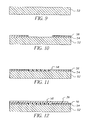
- FIG. 9 shows a substrate 52 of, say, a 550 ⁇ m thick single crystal silicon wafer for example.
- the substrate will be used to support the electrode structure and to form fluid conduits 48 that bring the fluid to nozzle orifice 22 , and the second fluid paths 50 that bring the dielectric fluid to region 34 .
- FIG. 10 shows the preferred embodiment after deposition, patterning, and etching of a first structural layer 54 (e.g. 0.75 ⁇ m thick doped polysilicon) and a first passivation layer 56 formed for example of 0.1 ⁇ m low pressure chemical vapor deposition (LPCVD) silicon nitride.
- first structural layer 54 e.g. 0.75 ⁇ m thick doped polysilicon
- first passivation layer 56 formed for example of 0.1 ⁇ m low pressure chemical vapor deposition (LPCVD) silicon nitride.
- LPCVD low pressure chemical vapor deposition
- the Sacrificial layer may be, for example, 0.85 ⁇ m plasma enhanced chemical vapor deposition (PECVD) silicon dioxide, filling in the depression formed during the previous etch and providing a planar surface for the deposition of addressable electrode 36 as shown in FIG. 12 .
- Addressable electrode 36 maybe 3 ⁇ m to 5 ⁇ m doped polysilicon, and is relatively thick for a microdevice because it is
- FIG. 13 shows the preferred embodiment after deposition, patterning, and etching of a subsequent sacrificial layer 60 (e.g. 0.1 ⁇ m silicon dioxide).
- This thin layer provides mechanical separation between addressable electrode 36 and central electrode 38 shown in FIG. 15 .
- subsequent sacrificial layer 60 is eliminated, the layers above will be attached to the layers below.
- the hole etched in the center will allow addressable electrode 36 and addressable electrode 28 can be mechanically coupled.
- the hole is preferably etched in the center, but could be etched elsewhere.
- FIG. 14 shows the preferred embodiment after deposition, patterning, and etching of a second passivation layer 62 (e.g. 0.1 ⁇ m LPCVD silicon nitride).
- This layer provides electrical separation between addressable electrode 36 and central electrode 38 , FIG. 15 .
- LPCVD nitride is preferable to PECVD nitride in this layer, since the breakdown voltage of LPCVD nitride is higher, allowing a larger voltage to be supported without current leakage for the same layer thickness.
- FIG. 15 shows the sequence for deposition, patterning, and etching of central electrode 38 (e.g. 5 ⁇ m doped polysilicon) and a third passivation layer 64 (e.g. 0.1 ⁇ m LPCVD silicon nitride).
- FIGS. 16 a and 16 b show the preferred embodiment after deposition, patterning, and etching of a third sacrificial layer 66 (e.g. 0.55 ⁇ m silicon dioxide). This layer provides mechanical separation between central electrode 38 and addressable electrode 28 , as well as separation between rigid coupler 40 (FIG. 17 b ) and the central electrode 38 .
- the patterning of the third sacrificial layer also removes part of the second sacrificial layer and exposes part of the first electrode.
- FIGS. 17 a - 17 c show the sequence for deposition, planarization (e.g. CMP), patterning, and etching of a fourth passivation layer 68 (e.g. 5 ⁇ m silicon nitride).
- This layer forms the rigid coupler 40 that mechanically couples addressable electrode 36 and addressable electrode 28 , while insulating them from one another.
- addressable electrode 28 (e.g. 2.5 ⁇ m doped polysilicon) has been deposited, patterned and etched.
- FIG. 19 shows the preferred embodiment after deposition, patterning, and etching of a fourth sacrificial layer 70 (e.g. 5 ⁇ m polyimide or silicon dioxide).
- This layer provides separation between addressable electrode 28 and nozzle plate 24 (FIG. 20) through which a drop will be ejected.
- the fourth sacrificial layer 70 will be eliminated later to form the liquid chamber 30 .
- This layer is etched twice; once to provide a dimple that will create flow restrictor 46 (FIG. 8 ), and once to expose addressable electrode 28 for mechanical attachment.
- nozzle plate 24 of, for example, 4 ⁇ m nitride or polyimide (if not used for the fourth sacrificial layer) has been deposited, patterned and etched.
- the hole in this layer forms nozzle orifice 22 through which the drop is ejected.
- FIG. 21 shows the preferred embodiment after substrate 52 is etched from the back side (the side not previously patterned), opening holes to first passivation layer 56 and first sacrificial layer 58 , which act as etch stops during this process.
- FIG. 22 shows the preferred embodiment after all sacrificial layers 58 , 60 , 66 , 70 are removed (e.g. by immersion in HF to remove silicon dioxide sacrificial layers and/or by oxygen plasma to eliminate polyimide sacrificial layers). This is the completed device.
- Central electrode 38 is provided with external power through the lead 42 in this cross-section.
- FIG. 23 shows a cross-section through B-B′ of the preferred embodiment in its finished state. The difference between this and the previous figure is the electrode structure on the left side, where addressable electrode 36 is provided with external power through lead 42 in this cross-section.
- FIG. 24 shows a cross-section through C-C′ of the preferred embodiment in its finished state.
- FIG. 25 shows a cross-section through D-D′ of the preferred embodiment in its finished state.
- the difference between this and the previous figure is that the region shown does not intersect any of the lead structure. This represents the region through which the fluid flows freely from the fluid conduit to the ejection chamber.
- FIGS. 26-28 are cross-sectional views taken through lines E-E′, F-F′ and G-G′, respectively, of FIG. 22 .
Abstract
Description
Claims (4)
Priority Applications (3)
| Application Number | Priority Date | Filing Date | Title |
|---|---|---|---|
| US10/191,506 US6830701B2 (en) | 2002-07-09 | 2002-07-09 | Method for fabricating microelectromechanical structures for liquid emission devices |
| JP2003176428A JP2004050830A (en) | 2002-07-09 | 2003-06-20 | Method for assembling small electrical machine structure in liquid ejector |
| EP03076996A EP1380427A3 (en) | 2002-07-09 | 2003-06-27 | Method for fabricating microelectromechanical structures for liquid emission devices |
Applications Claiming Priority (1)
| Application Number | Priority Date | Filing Date | Title |
|---|---|---|---|
| US10/191,506 US6830701B2 (en) | 2002-07-09 | 2002-07-09 | Method for fabricating microelectromechanical structures for liquid emission devices |
Publications (2)
| Publication Number | Publication Date |
|---|---|
| US20040008238A1 US20040008238A1 (en) | 2004-01-15 |
| US6830701B2 true US6830701B2 (en) | 2004-12-14 |
Family
ID=29735292
Family Applications (1)
| Application Number | Title | Priority Date | Filing Date |
|---|---|---|---|
| US10/191,506 Expired - Fee Related US6830701B2 (en) | 2002-07-09 | 2002-07-09 | Method for fabricating microelectromechanical structures for liquid emission devices |
Country Status (3)
| Country | Link |
|---|---|
| US (1) | US6830701B2 (en) |
| EP (1) | EP1380427A3 (en) |
| JP (1) | JP2004050830A (en) |
Cited By (5)
| Publication number | Priority date | Publication date | Assignee | Title |
|---|---|---|---|---|
| US20040046837A1 (en) * | 2002-09-05 | 2004-03-11 | Xerox Corporation | Systems and methods for microelectromechanical system based fluid ejection |
| US20070183015A1 (en) * | 2006-02-07 | 2007-08-09 | Jacobs Adrian M S | Spatial light modulator and a display device |
| US20070227863A1 (en) * | 2004-12-17 | 2007-10-04 | Samsung Electronics Co., Ltd. | Mems switch and method of fabricating the same |
| US20090046130A1 (en) * | 2007-08-16 | 2009-02-19 | Radominski George Z | Electrostatic Actuator And Fabrication Method |
| US20100247766A1 (en) * | 2009-03-25 | 2010-09-30 | University Of Michigan | Nozzle geometry for organic vapor jet printing |
Families Citing this family (5)
| Publication number | Priority date | Publication date | Assignee | Title |
|---|---|---|---|---|
| US6830701B2 (en) * | 2002-07-09 | 2004-12-14 | Eastman Kodak Company | Method for fabricating microelectromechanical structures for liquid emission devices |
| US6700173B1 (en) * | 2002-08-20 | 2004-03-02 | Memx, Inc. | Electrically isolated support for overlying MEM structure |
| US6770211B2 (en) * | 2002-08-30 | 2004-08-03 | Eastman Kodak Company | Fabrication of liquid emission device with asymmetrical electrostatic mandrel |
| JP2006007560A (en) * | 2004-06-25 | 2006-01-12 | Sony Corp | Functional element, its manufacturing method, fluid discharging apparatus, and printer |
| KR102574711B1 (en) * | 2021-05-07 | 2023-09-07 | 한국생산기술연구원 | Electrohydrodynamic nozzle chip based on mems fabrication, the method of manufacturing thereof and nozzle head module |
Citations (23)
| Publication number | Priority date | Publication date | Assignee | Title |
|---|---|---|---|---|
| US4520375A (en) * | 1983-05-13 | 1985-05-28 | Eaton Corporation | Fluid jet ejector |
| US4908679A (en) | 1981-01-23 | 1990-03-13 | National Semiconductor Corporation | Low resistance Schottky diode on polysilicon/metal-silicide |
| WO1990009677A1 (en) | 1989-02-16 | 1990-08-23 | Wisconsin Alumni Research Foundation | Formation of microstructures with removal of liquid by freezing and sublimation |
| US5051643A (en) * | 1990-08-30 | 1991-09-24 | Motorola, Inc. | Electrostatically switched integrated relay and capacitor |
| US5300444A (en) | 1988-09-14 | 1994-04-05 | Mitsubishi Denki Kabushiki Kaisha | Method of manufacturing a semiconductor device having a stacked structure formed of polycrystalline silicon film and silicon oxide film |
| US5644341A (en) | 1993-07-14 | 1997-07-01 | Seiko Epson Corporation | Ink jet head drive apparatus and drive method, and a printer using these |
| US5668579A (en) | 1993-06-16 | 1997-09-16 | Seiko Epson Corporation | Apparatus for and a method of driving an ink jet head having an electrostatic actuator |
| US5739831A (en) | 1994-09-16 | 1998-04-14 | Seiko Epson Corporation | Electric field driven ink jet printer having a resilient plate deformable by an electrostatic attraction force between spaced apart electrodes |
| US5798283A (en) | 1995-09-06 | 1998-08-25 | Sandia Corporation | Method for integrating microelectromechanical devices with electronic circuitry |
| US5804084A (en) | 1996-10-11 | 1998-09-08 | Sandia Corporation | Use of chemical mechanical polishing in micromachining |
| US5890745A (en) | 1997-01-29 | 1999-04-06 | The Board Of Trustees Of The Leland Stanford Junior University | Micromachined fluidic coupler |
| US5907791A (en) | 1996-04-25 | 1999-05-25 | Lucent Technologies Inc. | Method of making semiconductor devices by patterning a wafer having a non-planar surface |
| US6082208A (en) | 1998-04-01 | 2000-07-04 | Sandia Corporation | Method for fabricating five-level microelectromechanical structures and microelectromechanical transmission formed |
| US6127198A (en) | 1998-10-15 | 2000-10-03 | Xerox Corporation | Method of fabricating a fluid drop ejector |
| US6174820B1 (en) | 1999-02-16 | 2001-01-16 | Sandia Corporation | Use of silicon oxynitride as a sacrificial material for microelectromechanical devices |
| US20010023523A1 (en) | 1998-10-15 | 2001-09-27 | Xerox Corporation | Method of fabricating a micro-electro-mechanical fluid ejector |
| US6318841B1 (en) | 1998-10-15 | 2001-11-20 | Xerox Corporation | Fluid drop ejector |
| US6345884B1 (en) | 1999-11-04 | 2002-02-12 | Samsung Electronics Co., Ltd. | Electrostatic attraction type ink jetting apparatus and a method for manufacturing the same |
| US6357865B1 (en) | 1998-10-15 | 2002-03-19 | Xerox Corporation | Micro-electro-mechanical fluid ejector and method of operating same |
| US6527373B1 (en) * | 2002-04-15 | 2003-03-04 | Eastman Kodak Company | Drop-on-demand liquid emission using interconnected dual electrodes as ejection device |
| US20040008238A1 (en) * | 2002-07-09 | 2004-01-15 | Eastman Kodak Company | Method for fabricating microelectromechanical structures for liquid emission devices |
| US20040036740A1 (en) * | 2002-08-26 | 2004-02-26 | Eastman Kodak Company | Fabricating liquid emission electrostatic device using symmetrical mandrel |
| US20040041884A1 (en) * | 2002-08-30 | 2004-03-04 | Eastman Kodak Company | Fabrication of liquid emission device with asymmetrical electrostatic mandrel |
Family Cites Families (2)
| Publication number | Priority date | Publication date | Assignee | Title |
|---|---|---|---|---|
| US6126140A (en) * | 1997-12-29 | 2000-10-03 | Honeywell International Inc. | Monolithic bi-directional microvalve with enclosed drive electric field |
| US6676249B2 (en) * | 1999-12-17 | 2004-01-13 | Eastman Kodak Company | Continuous color ink jet print head apparatus and method |
-
2002
- 2002-07-09 US US10/191,506 patent/US6830701B2/en not_active Expired - Fee Related
-
2003
- 2003-06-20 JP JP2003176428A patent/JP2004050830A/en active Pending
- 2003-06-27 EP EP03076996A patent/EP1380427A3/en not_active Withdrawn
Patent Citations (23)
| Publication number | Priority date | Publication date | Assignee | Title |
|---|---|---|---|---|
| US4908679A (en) | 1981-01-23 | 1990-03-13 | National Semiconductor Corporation | Low resistance Schottky diode on polysilicon/metal-silicide |
| US4520375A (en) * | 1983-05-13 | 1985-05-28 | Eaton Corporation | Fluid jet ejector |
| US5300444A (en) | 1988-09-14 | 1994-04-05 | Mitsubishi Denki Kabushiki Kaisha | Method of manufacturing a semiconductor device having a stacked structure formed of polycrystalline silicon film and silicon oxide film |
| WO1990009677A1 (en) | 1989-02-16 | 1990-08-23 | Wisconsin Alumni Research Foundation | Formation of microstructures with removal of liquid by freezing and sublimation |
| US5051643A (en) * | 1990-08-30 | 1991-09-24 | Motorola, Inc. | Electrostatically switched integrated relay and capacitor |
| US5668579A (en) | 1993-06-16 | 1997-09-16 | Seiko Epson Corporation | Apparatus for and a method of driving an ink jet head having an electrostatic actuator |
| US5644341A (en) | 1993-07-14 | 1997-07-01 | Seiko Epson Corporation | Ink jet head drive apparatus and drive method, and a printer using these |
| US5739831A (en) | 1994-09-16 | 1998-04-14 | Seiko Epson Corporation | Electric field driven ink jet printer having a resilient plate deformable by an electrostatic attraction force between spaced apart electrodes |
| US5798283A (en) | 1995-09-06 | 1998-08-25 | Sandia Corporation | Method for integrating microelectromechanical devices with electronic circuitry |
| US5907791A (en) | 1996-04-25 | 1999-05-25 | Lucent Technologies Inc. | Method of making semiconductor devices by patterning a wafer having a non-planar surface |
| US5804084A (en) | 1996-10-11 | 1998-09-08 | Sandia Corporation | Use of chemical mechanical polishing in micromachining |
| US5890745A (en) | 1997-01-29 | 1999-04-06 | The Board Of Trustees Of The Leland Stanford Junior University | Micromachined fluidic coupler |
| US6082208A (en) | 1998-04-01 | 2000-07-04 | Sandia Corporation | Method for fabricating five-level microelectromechanical structures and microelectromechanical transmission formed |
| US6127198A (en) | 1998-10-15 | 2000-10-03 | Xerox Corporation | Method of fabricating a fluid drop ejector |
| US20010023523A1 (en) | 1998-10-15 | 2001-09-27 | Xerox Corporation | Method of fabricating a micro-electro-mechanical fluid ejector |
| US6318841B1 (en) | 1998-10-15 | 2001-11-20 | Xerox Corporation | Fluid drop ejector |
| US6357865B1 (en) | 1998-10-15 | 2002-03-19 | Xerox Corporation | Micro-electro-mechanical fluid ejector and method of operating same |
| US6174820B1 (en) | 1999-02-16 | 2001-01-16 | Sandia Corporation | Use of silicon oxynitride as a sacrificial material for microelectromechanical devices |
| US6345884B1 (en) | 1999-11-04 | 2002-02-12 | Samsung Electronics Co., Ltd. | Electrostatic attraction type ink jetting apparatus and a method for manufacturing the same |
| US6527373B1 (en) * | 2002-04-15 | 2003-03-04 | Eastman Kodak Company | Drop-on-demand liquid emission using interconnected dual electrodes as ejection device |
| US20040008238A1 (en) * | 2002-07-09 | 2004-01-15 | Eastman Kodak Company | Method for fabricating microelectromechanical structures for liquid emission devices |
| US20040036740A1 (en) * | 2002-08-26 | 2004-02-26 | Eastman Kodak Company | Fabricating liquid emission electrostatic device using symmetrical mandrel |
| US20040041884A1 (en) * | 2002-08-30 | 2004-03-04 | Eastman Kodak Company | Fabrication of liquid emission device with asymmetrical electrostatic mandrel |
Cited By (13)
| Publication number | Priority date | Publication date | Assignee | Title |
|---|---|---|---|---|
| US20040046837A1 (en) * | 2002-09-05 | 2004-03-11 | Xerox Corporation | Systems and methods for microelectromechanical system based fluid ejection |
| US7105131B2 (en) * | 2002-09-05 | 2006-09-12 | Xerox Corporation | Systems and methods for microelectromechanical system based fluid ejection |
| US20070227863A1 (en) * | 2004-12-17 | 2007-10-04 | Samsung Electronics Co., Ltd. | Mems switch and method of fabricating the same |
| US7342710B2 (en) * | 2004-12-17 | 2008-03-11 | Samsung Electronics Co., Ltd. | Mems switch and method of fabricating the same |
| US20070183015A1 (en) * | 2006-02-07 | 2007-08-09 | Jacobs Adrian M S | Spatial light modulator and a display device |
| US7359105B2 (en) * | 2006-02-07 | 2008-04-15 | Sharp Kabushiki Kaisha | Spatial light modulator and a display device |
| US20090046130A1 (en) * | 2007-08-16 | 2009-02-19 | Radominski George Z | Electrostatic Actuator And Fabrication Method |
| WO2009025985A1 (en) * | 2007-08-16 | 2009-02-26 | Hewlett-Packard Development Company, L.P. | Electrostatic actuator and fabrication method |
| US7677706B2 (en) | 2007-08-16 | 2010-03-16 | Hewlett-Packard Development Company, L.P. | Electrostatic actuator and fabrication method |
| US20100247766A1 (en) * | 2009-03-25 | 2010-09-30 | University Of Michigan | Nozzle geometry for organic vapor jet printing |
| US8931431B2 (en) * | 2009-03-25 | 2015-01-13 | The Regents Of The University Of Michigan | Nozzle geometry for organic vapor jet printing |
| US10480056B2 (en) * | 2009-03-25 | 2019-11-19 | The Regents Of The University Of Michigan | Nozzle geometry for organic vapor jet printing |
| US10941481B2 (en) | 2009-03-25 | 2021-03-09 | The Regents Of The University Of Michigan | Nozzle geometry for organic vapor jet printing |
Also Published As
| Publication number | Publication date |
|---|---|
| US20040008238A1 (en) | 2004-01-15 |
| EP1380427A3 (en) | 2004-06-16 |
| EP1380427A2 (en) | 2004-01-14 |
| JP2004050830A (en) | 2004-02-19 |
Similar Documents
| Publication | Publication Date | Title |
|---|---|---|
| US6508947B2 (en) | Method for fabricating a micro-electro-mechanical fluid ejector | |
| US6572218B2 (en) | Electrostatically-actuated device having a corrugated multi-layer membrane structure | |
| TWI450827B (en) | Actuator | |
| US6830701B2 (en) | Method for fabricating microelectromechanical structures for liquid emission devices | |
| US6863382B2 (en) | Liquid emission device having membrane with individually deformable portions, and methods of operating and manufacturing same | |
| JP4894603B2 (en) | Manufacturing method of flow path substrate, manufacturing method of liquid droplet ejection head, and manufacturing method of liquid droplet ejection device | |
| US6966110B2 (en) | Fabrication of liquid emission device with symmetrical electrostatic mandrel | |
| US6770211B2 (en) | Fabrication of liquid emission device with asymmetrical electrostatic mandrel | |
| US6938310B2 (en) | Method of making a multi-layer micro-electromechanical electrostatic actuator for producing drop-on-demand liquid emission devices | |
| CN105667087B (en) | The method for being used to form inkjet print head and the ink-jet printer including it | |
| US6874867B2 (en) | Electrostatically actuated drop ejector | |
| US6715704B2 (en) | Drop-on-demand liquid emission using asymmetrical electrostatic device | |
| JP4480956B2 (en) | Discharge device for droplet discharge | |
| EP1393909B1 (en) | Drop-on-demand liquid emission using symmetrical electrostatic device |
Legal Events
| Date | Code | Title | Description |
|---|---|---|---|
| AS | Assignment |
Owner name: EASTMAN KODAK COMPANY, NEW YORK Free format text: ASSIGNMENT OF ASSIGNORS INTEREST;ASSIGNORS:DEBAR, MICHAEL J.;DELAMETTER, CHRISTOPHER N.;FURLANI, EDWARD P.;REEL/FRAME:013103/0036 Effective date: 20020709 |
|
| FEPP | Fee payment procedure |
Free format text: PAYOR NUMBER ASSIGNED (ORIGINAL EVENT CODE: ASPN); ENTITY STATUS OF PATENT OWNER: LARGE ENTITY |
|
| FPAY | Fee payment |
Year of fee payment: 4 |
|
| AS | Assignment |
Owner name: CITICORP NORTH AMERICA, INC., AS AGENT, NEW YORK Free format text: SECURITY INTEREST;ASSIGNORS:EASTMAN KODAK COMPANY;PAKON, INC.;REEL/FRAME:028201/0420 Effective date: 20120215 |
|
| FPAY | Fee payment |
Year of fee payment: 8 |
|
| AS | Assignment |
Owner name: WILMINGTON TRUST, NATIONAL ASSOCIATION, AS AGENT, MINNESOTA Free format text: PATENT SECURITY AGREEMENT;ASSIGNORS:EASTMAN KODAK COMPANY;PAKON, INC.;REEL/FRAME:030122/0235 Effective date: 20130322 Owner name: WILMINGTON TRUST, NATIONAL ASSOCIATION, AS AGENT, Free format text: PATENT SECURITY AGREEMENT;ASSIGNORS:EASTMAN KODAK COMPANY;PAKON, INC.;REEL/FRAME:030122/0235 Effective date: 20130322 |
|
| AS | Assignment |
Owner name: PAKON, INC., NEW YORK Free format text: RELEASE OF SECURITY INTEREST IN PATENTS;ASSIGNORS:CITICORP NORTH AMERICA, INC., AS SENIOR DIP AGENT;WILMINGTON TRUST, NATIONAL ASSOCIATION, AS JUNIOR DIP AGENT;REEL/FRAME:031157/0451 Effective date: 20130903 Owner name: BARCLAYS BANK PLC, AS ADMINISTRATIVE AGENT, NEW YORK Free format text: INTELLECTUAL PROPERTY SECURITY AGREEMENT (SECOND LIEN);ASSIGNORS:EASTMAN KODAK COMPANY;FAR EAST DEVELOPMENT LTD.;FPC INC.;AND OTHERS;REEL/FRAME:031159/0001 Effective date: 20130903 Owner name: JPMORGAN CHASE BANK, N.A., AS ADMINISTRATIVE, DELAWARE Free format text: INTELLECTUAL PROPERTY SECURITY AGREEMENT (FIRST LIEN);ASSIGNORS:EASTMAN KODAK COMPANY;FAR EAST DEVELOPMENT LTD.;FPC INC.;AND OTHERS;REEL/FRAME:031158/0001 Effective date: 20130903 Owner name: BANK OF AMERICA N.A., AS AGENT, MASSACHUSETTS Free format text: INTELLECTUAL PROPERTY SECURITY AGREEMENT (ABL);ASSIGNORS:EASTMAN KODAK COMPANY;FAR EAST DEVELOPMENT LTD.;FPC INC.;AND OTHERS;REEL/FRAME:031162/0117 Effective date: 20130903 Owner name: JPMORGAN CHASE BANK, N.A., AS ADMINISTRATIVE, DELA Free format text: INTELLECTUAL PROPERTY SECURITY AGREEMENT (FIRST LIEN);ASSIGNORS:EASTMAN KODAK COMPANY;FAR EAST DEVELOPMENT LTD.;FPC INC.;AND OTHERS;REEL/FRAME:031158/0001 Effective date: 20130903 Owner name: BARCLAYS BANK PLC, AS ADMINISTRATIVE AGENT, NEW YO Free format text: INTELLECTUAL PROPERTY SECURITY AGREEMENT (SECOND LIEN);ASSIGNORS:EASTMAN KODAK COMPANY;FAR EAST DEVELOPMENT LTD.;FPC INC.;AND OTHERS;REEL/FRAME:031159/0001 Effective date: 20130903 Owner name: EASTMAN KODAK COMPANY, NEW YORK Free format text: RELEASE OF SECURITY INTEREST IN PATENTS;ASSIGNORS:CITICORP NORTH AMERICA, INC., AS SENIOR DIP AGENT;WILMINGTON TRUST, NATIONAL ASSOCIATION, AS JUNIOR DIP AGENT;REEL/FRAME:031157/0451 Effective date: 20130903 |
|
| REMI | Maintenance fee reminder mailed | ||
| LAPS | Lapse for failure to pay maintenance fees | ||
| STCH | Information on status: patent discontinuation |
Free format text: PATENT EXPIRED DUE TO NONPAYMENT OF MAINTENANCE FEES UNDER 37 CFR 1.362 |
|
| FP | Lapsed due to failure to pay maintenance fee |
Effective date: 20161214 |
|
| AS | Assignment |
Owner name: PAKON, INC., NEW YORK Free format text: RELEASE BY SECURED PARTY;ASSIGNOR:JP MORGAN CHASE BANK, N.A., AS ADMINISTRATIVE AGENT;REEL/FRAME:049814/0001 Effective date: 20190617 Owner name: KODAK PHILIPPINES, LTD., NEW YORK Free format text: RELEASE BY SECURED PARTY;ASSIGNOR:JP MORGAN CHASE BANK, N.A., AS ADMINISTRATIVE AGENT;REEL/FRAME:049814/0001 Effective date: 20190617 Owner name: KODAK IMAGING NETWORK, INC., NEW YORK Free format text: RELEASE BY SECURED PARTY;ASSIGNOR:JP MORGAN CHASE BANK, N.A., AS ADMINISTRATIVE AGENT;REEL/FRAME:049814/0001 Effective date: 20190617 Owner name: CREO MANUFACTURING AMERICA LLC, NEW YORK Free format text: RELEASE BY SECURED PARTY;ASSIGNOR:JP MORGAN CHASE BANK, N.A., AS ADMINISTRATIVE AGENT;REEL/FRAME:049814/0001 Effective date: 20190617 Owner name: NPEC, INC., NEW YORK Free format text: RELEASE BY SECURED PARTY;ASSIGNOR:JP MORGAN CHASE BANK, N.A., AS ADMINISTRATIVE AGENT;REEL/FRAME:049814/0001 Effective date: 20190617 Owner name: QUALEX, INC., NEW YORK Free format text: RELEASE BY SECURED PARTY;ASSIGNOR:JP MORGAN CHASE BANK, N.A., AS ADMINISTRATIVE AGENT;REEL/FRAME:049814/0001 Effective date: 20190617 Owner name: KODAK (NEAR EAST), INC., NEW YORK Free format text: RELEASE BY SECURED PARTY;ASSIGNOR:JP MORGAN CHASE BANK, N.A., AS ADMINISTRATIVE AGENT;REEL/FRAME:049814/0001 Effective date: 20190617 Owner name: LASER PACIFIC MEDIA CORPORATION, NEW YORK Free format text: RELEASE BY SECURED PARTY;ASSIGNOR:JP MORGAN CHASE BANK, N.A., AS ADMINISTRATIVE AGENT;REEL/FRAME:049814/0001 Effective date: 20190617 Owner name: KODAK REALTY, INC., NEW YORK Free format text: RELEASE BY SECURED PARTY;ASSIGNOR:JP MORGAN CHASE BANK, N.A., AS ADMINISTRATIVE AGENT;REEL/FRAME:049814/0001 Effective date: 20190617 Owner name: KODAK AVIATION LEASING LLC, NEW YORK Free format text: RELEASE BY SECURED PARTY;ASSIGNOR:JP MORGAN CHASE BANK, N.A., AS ADMINISTRATIVE AGENT;REEL/FRAME:049814/0001 Effective date: 20190617 Owner name: FPC, INC., NEW YORK Free format text: RELEASE BY SECURED PARTY;ASSIGNOR:JP MORGAN CHASE BANK, N.A., AS ADMINISTRATIVE AGENT;REEL/FRAME:049814/0001 Effective date: 20190617 Owner name: FAR EAST DEVELOPMENT LTD., NEW YORK Free format text: RELEASE BY SECURED PARTY;ASSIGNOR:JP MORGAN CHASE BANK, N.A., AS ADMINISTRATIVE AGENT;REEL/FRAME:049814/0001 Effective date: 20190617 Owner name: KODAK PORTUGUESA LIMITED, NEW YORK Free format text: RELEASE BY SECURED PARTY;ASSIGNOR:JP MORGAN CHASE BANK, N.A., AS ADMINISTRATIVE AGENT;REEL/FRAME:049814/0001 Effective date: 20190617 Owner name: KODAK AMERICAS, LTD., NEW YORK Free format text: RELEASE BY SECURED PARTY;ASSIGNOR:JP MORGAN CHASE BANK, N.A., AS ADMINISTRATIVE AGENT;REEL/FRAME:049814/0001 Effective date: 20190617 Owner name: EASTMAN KODAK COMPANY, NEW YORK Free format text: RELEASE BY SECURED PARTY;ASSIGNOR:JP MORGAN CHASE BANK, N.A., AS ADMINISTRATIVE AGENT;REEL/FRAME:049814/0001 Effective date: 20190617 |
|
| AS | Assignment |
Owner name: LASER PACIFIC MEDIA CORPORATION, NEW YORK Free format text: RELEASE BY SECURED PARTY;ASSIGNOR:BARCLAYS BANK PLC;REEL/FRAME:052773/0001 Effective date: 20170202 Owner name: NPEC INC., NEW YORK Free format text: RELEASE BY SECURED PARTY;ASSIGNOR:BARCLAYS BANK PLC;REEL/FRAME:052773/0001 Effective date: 20170202 Owner name: KODAK PHILIPPINES LTD., NEW YORK Free format text: RELEASE BY SECURED PARTY;ASSIGNOR:BARCLAYS BANK PLC;REEL/FRAME:052773/0001 Effective date: 20170202 Owner name: QUALEX INC., NEW YORK Free format text: RELEASE BY SECURED PARTY;ASSIGNOR:BARCLAYS BANK PLC;REEL/FRAME:052773/0001 Effective date: 20170202 Owner name: FAR EAST DEVELOPMENT LTD., NEW YORK Free format text: RELEASE BY SECURED PARTY;ASSIGNOR:BARCLAYS BANK PLC;REEL/FRAME:052773/0001 Effective date: 20170202 Owner name: FPC INC., NEW YORK Free format text: RELEASE BY SECURED PARTY;ASSIGNOR:BARCLAYS BANK PLC;REEL/FRAME:052773/0001 Effective date: 20170202 Owner name: KODAK (NEAR EAST) INC., NEW YORK Free format text: RELEASE BY SECURED PARTY;ASSIGNOR:BARCLAYS BANK PLC;REEL/FRAME:052773/0001 Effective date: 20170202 Owner name: KODAK AMERICAS LTD., NEW YORK Free format text: RELEASE BY SECURED PARTY;ASSIGNOR:BARCLAYS BANK PLC;REEL/FRAME:052773/0001 Effective date: 20170202 Owner name: EASTMAN KODAK COMPANY, NEW YORK Free format text: RELEASE BY SECURED PARTY;ASSIGNOR:BARCLAYS BANK PLC;REEL/FRAME:052773/0001 Effective date: 20170202 Owner name: KODAK REALTY INC., NEW YORK Free format text: RELEASE BY SECURED PARTY;ASSIGNOR:BARCLAYS BANK PLC;REEL/FRAME:052773/0001 Effective date: 20170202 |