US6839474B2 - Optical assembly for coupling with integrated optical devices and method for making - Google Patents
Optical assembly for coupling with integrated optical devices and method for making Download PDFInfo
- Publication number
- US6839474B2 US6839474B2 US09/987,766 US98776601A US6839474B2 US 6839474 B2 US6839474 B2 US 6839474B2 US 98776601 A US98776601 A US 98776601A US 6839474 B2 US6839474 B2 US 6839474B2
- Authority
- US
- United States
- Prior art keywords
- optical
- assembly
- chip
- array
- substrate
- Prior art date
- Legal status (The legal status is an assumption and is not a legal conclusion. Google has not performed a legal analysis and makes no representation as to the accuracy of the status listed.)
- Expired - Fee Related, expires
Links
Images


Classifications
-
- G—PHYSICS
- G02—OPTICS
- G02B—OPTICAL ELEMENTS, SYSTEMS OR APPARATUS
- G02B6/00—Light guides; Structural details of arrangements comprising light guides and other optical elements, e.g. couplings
- G02B6/24—Coupling light guides
- G02B6/26—Optical coupling means
- G02B6/32—Optical coupling means having lens focusing means positioned between opposed fibre ends
- G02B6/322—Optical coupling means having lens focusing means positioned between opposed fibre ends and having centering means being part of the lens for the self-positioning of the lightguide at the focal point, e.g. holes, wells, indents, nibs
-
- G—PHYSICS
- G02—OPTICS
- G02B—OPTICAL ELEMENTS, SYSTEMS OR APPARATUS
- G02B6/00—Light guides; Structural details of arrangements comprising light guides and other optical elements, e.g. couplings
- G02B6/24—Coupling light guides
- G02B6/26—Optical coupling means
- G02B6/30—Optical coupling means for use between fibre and thin-film device
-
- G—PHYSICS
- G02—OPTICS
- G02B—OPTICAL ELEMENTS, SYSTEMS OR APPARATUS
- G02B6/00—Light guides; Structural details of arrangements comprising light guides and other optical elements, e.g. couplings
- G02B6/24—Coupling light guides
- G02B6/42—Coupling light guides with opto-electronic elements
- G02B6/4201—Packages, e.g. shape, construction, internal or external details
- G02B6/4219—Mechanical fixtures for holding or positioning the elements relative to each other in the couplings; Alignment methods for the elements, e.g. measuring or observing methods especially used therefor
- G02B6/4228—Passive alignment, i.e. without a detection of the degree of coupling or the position of the elements
-
- G—PHYSICS
- G02—OPTICS
- G02B—OPTICAL ELEMENTS, SYSTEMS OR APPARATUS
- G02B6/00—Light guides; Structural details of arrangements comprising light guides and other optical elements, e.g. couplings
- G02B6/24—Coupling light guides
- G02B6/42—Coupling light guides with opto-electronic elements
- G02B6/4201—Packages, e.g. shape, construction, internal or external details
- G02B6/4219—Mechanical fixtures for holding or positioning the elements relative to each other in the couplings; Alignment methods for the elements, e.g. measuring or observing methods especially used therefor
- G02B6/4236—Fixing or mounting methods of the aligned elements
- G02B6/4239—Adhesive bonding; Encapsulation with polymer material
Definitions
- GRIN lenses are sometimes utilized for efficient optical coupling to integrated optical devices, especially for coupling between optical fibers and integrated optical waveguides having a high delta n.
- the alignment of an optical fiber with a GRIN lens and an integrated optical device is complicated because three independent devices must be fixed at a point in space in such a way to provide optimal alignment.
- the invention provides an optical assembly that includes a substrate with an upper surface and a cut-out portion, an optical array mounted on the upper surface, and an imaging assembly positioned at least partially within the cut-out portion.
- the imaging assembly includes at least one imaging device mounted on a first chip.
- the optical array is optically coupled to the imaging assembly.
- the invention further provides an optical assembly having a notch which serves as a wick stop.
- the optical assembly includes a substrate with an upper surface, an optical array mounted on the upper surface, an integrated optic chip mounted on the upper surface, and a waveguide mounted on the integrated optic chip.
- the waveguide includes at least one waveguide core encased within a cladding.
- the optical array is optically coupled to the integrated optic chip through the waveguide.
- the invention further provides a method for assembling an optical assembly that includes a substrate having an upper surface and a cut-out portion, an optical array, and an imaging assembly.
- the method includes the steps of positioning the optical array on the substrate upper surface, lowering the imaging assembly at least partially within the cut-out portion, optically coupling the optical array with the imaging assembly, and affixing the imaging assembly to the substrate and the optical array to the imaging assembly.
- FIG. 1 is a side view showing the assembly of an optical assembly in accordance with an embodiment of the invention.
- FIG. 2 is a perspective view of a portion of the optical assembly of FIG. 1 .
- FIG. 3 is another perspective view like FIG. 2 .
- FIG. 4 is another side view showing the optical assembly of FIG. 1 in an assembled state.
- FIG. 5 is a perspective view of a portion of an optical assembly constructed in accordance with another embodiment of the invention.
- FIG. 6 is a cross-sectional view of the optical assembly of FIG. 5 .
- FIG. 7 is a top view of a lapping apparatus for smoothing the ends of an imaging assembly, such as the imaging assembly of FIGS. 1 and 6 .
- FIG. 8 is a perspective view of a portion of an optical assembly constructed in accordance with another embodiment of the invention.
- FIGS. 9-11 are perspective views showing the assembly of a portion of an optical assembly in accordance with another embodiment of the invention.
- FIGS. 12-13 are side views showing the assembly of an optical assembly constructed in accordance with another embodiment of the invention.
- FIG. 14 is a perspective view showing the assembly of a portion of the optical assembly of FIGS. 12-13 .
- FIG. 15 is a side view of an optical assembly constructed in accordance with another embodiment of the invention.
- FIG. 16 is a side view of an optical assembly constructed in accordance with another embodiment of the invention.
- FIG. 17 is a side view of an optical assembly constructed in accordance with another embodiment of the invention.
- FIG. 18 is a front view of the optical assembly of FIG. 17 .
- FIG. 19 is a side view of an optical assembly constructed in accordance with another embodiment of the invention.
- FIG. 20 is a perspective view of a portion of an optical assembly constructed in accordance with another embodiment of the invention.
- FIG. 21 is a side view of an assembled optical assembly including the portion of the optical assembly of FIG. 20 .
- FIG. 22 is a perspective view showing the assembly of an optical assembly in accordance with another embodiment of the invention.
- FIG. 23 is a perspective view of an optical assembly constructed in accordance with another embodiment of the invention.
- FIG. 24 is a side view of the portion of the optical assembly of FIG. 23 .
- FIG. 25 is a perspective view of a portion of an optical assembly constructed in accordance with another embodiment of the invention.
- FIG. 26 is a side view of the portion of the optical assembly of FIG. 25 .
- FIG. 27 is a side view of an optical assembly constructed in accordance with another embodiment of the invention.
- FIG. 28 is a side view of an optical assembly constructed in accordance with another embodiment of the invention.
- FIG. 29 is a side view showing the assembly of an optical assembly in accordance with another embodiment of the invention.
- FIG. 30 is a side view of an optical assembly constructed in accordance with another embodiment of the invention.
- FIG. 31 is a front view of an optical assembly constructed in accordance with another embodiment of the invention.
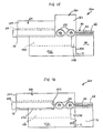
- an optical assembly 10 which includes an optical fiber array 20 , a substrate 30 , an optical waveguide 40 , and an imaging assembly 50 .
- the optical fiber array 20 , the optical waveguide 40 , and the imaging assembly 50 are aligned to allow light to traverse along a path including an optical fiber, a GRIN lens, and a waveguide core (FIG. 4 ), as will be described in detail below.
- the optical fiber array 20 includes a fiber chip 22 with a plurality of V-grooves 24 on a surface thereof and a notch 26 aligned transverse to the V-grooves 24 .
- the V-grooves are sized and configured to each receive an optical fiber 28 , which may be held in place within the V-groove 24 with an adhesive material, such as a glue or an epoxy.
- Each optical fiber 28 has an end 29 .
- the notch 26 serves as a wick stop for the adhesive material.
- the optical fiber array 20 may, instead, be replaced with another optical array, such as an optical bench.
- the substrate 30 includes an upper surface 31 in which a plurality of V-grooves 32 are located.
- the V-grooves 32 are located to receive the optical fibers 28 .
- the substrate 30 further includes a valley 34 , which is a cut-out portion in the substrate which preferably is formed with a dicing saw or other similar device.
- the valley 34 has a width C (FIG. 2 ).
- the optical fiber 28 is positioned such that a portion A of the fiber 28 extends into the valley 34 .
- the portion A should have a length which is less than about five times the diameter of the optical fiber 28 . Preferably, the portion A should be less than about 600 microns in length.
- the imaging assembly 50 fits within the valley 34 .
- the waveguide 40 is located on the upper surface 31 opposite from where the optical fiber array 20 is positioned.
- the waveguide 40 includes a plurality of waveguide cores 42 encased within a cladding 44 . Each of the waveguide cores 42 has an end 46 .
- the imaging assembly 50 includes a lens chip 52 with a lower surface 53 , into which is positioned a plurality of V-grooves 54 .
- a GRIN lens 56 is located within each V-groove 54 .
- the GRIN lenses 56 each have a first end 58 and a second end 59 .
- the imaging assembly 50 has a width B which is less than the width C of the valley 34 . Preferably, the width B is between about 25 and about 500 microns less than the width C of the valley 34 .
- the optical fiber array 20 is positioned in, but not adhered to, the V-grooves 32 of the substrate such that the portion A extends into the valley 34 .
- the imaging assembly 50 is then disposed into the valley 34 .
- the optical fiber array 20 is then moved to place the ends 29 of the optical fibers 28 flush with the first ends 58 of the GRIN lenses 56 and to place the second ends 59 of the GRIN lenses 56 flush with the ends 46 of the waveguide cores 42 .
- the imaging assembly 50 is moved in the direction D to obtain optimal optical power through the optical assembly 10 . It should be noted that in this position the imaging assembly 50 has two translational and one rotational degrees of freedom.
- the GRIN lenses 56 preferably do not contact the bottom surface of the valley 34 .
- an adhesive material 60 is placed in strategic locations to affix the optical fiber array 20 to the imaging assembly 50 and the imaging assembly 50 to the waveguide 40 and to the substrate 30 .
- the optical assembly 10 illustrated in FIGS. 1-4 is adapted to be affixed to an integrated optic chip.
- a preferred method of affixing is bonding.
- the illustrated optical assembly 10 includes GRIN lenses 56 , it should be appreciated that other types of imaging devices may be used. Specifically, the GRIN lenses 56 may be replaced with graded index fibers, or even short lengths of step-index fibers.
- FIGS. 5-6 illustrate an alternative embodiment, showing a portion of an optical assembly 100 having a substrate 130 .
- the substrate 130 has a cut-out portion which takes the form of a recessed area 132 positioned between a pair of ledges 134 .
- Each of the ledges 134 has an upper surface 136 which is in the same plane as the upper surface 31 .
- first and second notches 37 , 38 are positioned on either side of the ledges 134 .
- the notches 37 , 38 segregate various portions of the substrate 130 .
- the notches 37 , 38 are formed through the use of a dicing saw.
- the surfaces 136 provide a surface to which the imaging assembly 50 can be affixed, through the use of the adhesive material 60 .
- the GRIN lenses 56 do not contact any surfaces of the ledges 134 or the recessed area 132 .
- the notches 37 , 38 serve as wick stops to suppress flow of the adhesive material 60 used to adhere the imaging assembly 50 and the optical fiber array 20 to the substrate 30 .
- the adhesive material 60 is inhibited from flowing into the notches 37 , 38 due to surface tension.
- the notches 37 , 38 may also serve to receive index matching materials which are useful between the fibers 56 , the imaging assembly 50 and the waveguide assembly 40 .
- adhesive materials such as the adhesive material 60
- adhesive materials are inhibited from being in the light path from the optical fiber array 20 through the waveguide assembly 40
- low cost adhesive materials namely adhesive materials which are not optical quality
- index matching materials may be used, such materials need not also have adhesive characteristics, and may instead be a non-adhesive gel.
- FIG. 7 illustrates a device which smoothes each side of the GRIN lenses 56 .
- the smoothing, or lapping, device includes a top lapping plate 70 and a bottom lapping plate 72 .
- the top lapping plate 70 smoothes the first end 58 of the GRIN lenses 56
- the bottom lapping plate 72 smoothes the second end 59 of the GRIN lenses 56 .
- FIG. 8 illustrates a portion of an optical assembly 200 , which includes a substrate 230 .
- the substrate 230 does not include the V-grooves 32 (FIGS. 1 - 4 ). Instead, the optical fiber array 20 is aligned with the imaging assembly 50 and the waveguide 40 , and the imaging assembly 50 is affixed to the waveguide 40 and the surfaces 136 . The optical fiber array 20 is then affixed to the imaging assembly 50 , wholly unsupported by the substrate 230 .
- Notches 138 may be cut into the substrate 230 , separating the ledges 134 from the rest of the substrate 230 . The notches 138 may extend a greater distance into the substrate 230 than the lower surface of the recessed area 132 .
- FIGS. 9-11 show a portion of another optical assembly 300 constructed in accordance with an embodiment of the invention.
- the optical assembly 300 includes a substrate 330 , which includes the recessed area 132 between the ledges 134 , and an integrated optic chip 90 , which serves as a stable base for the waveguide 40 .
- the substrate 330 and the integrated optic chip 90 are moved together such that a side surface 333 of the substrate 330 is contacted with a surface 91 of the integrated optic chip 90 .
- An adhesive material 60 is utilized to affix the substrate 330 and the integrated optic chip 90 together.
- notches 238 may be diced into the substrate 330 . It is not necessary for the integrated optic chip 90 to be aligned accurately with the substrate 330 .
- the substrate 330 provides no passive alignment capability for either the optical fiber array 20 or the imaging assembly 50 .
- the imaging assembly 50 may be omitted in this illustrated embodiment, with the optical fibers 28 being coupled directly to the waveguide cores 42 .
- An advantage of the substrate 330 is that it may suppress the flow of the adhesive material 60 between the optical fibers 28 and the waveguide cores 42 , preventing the adhesive material 60 from interfering with the optical path.
- the notches 238 serve as a wick stop trench, further suppressing flow of the adhesive material.
- Another advantage of utilizing the substrate 330 is that it allows surface 91 of the integrated optic chip 90 to be polished.
- FIGS. 12-14 illustrate the assembly of another optical assembly 400 , which includes an optical fiber array 120 , the waveguide 40 , the imaging assembly 50 , and a substrate 430 .
- the optical fiber array 120 differs from the optical fiber array 20 in that it lacks the notch 26 .
- the substrate 430 has a greater width than the substrate 330 , and thereby allows the mounting of both the optical fiber array 120 and the imaging assembly 50 to an upper surface 236 thereof.
- the substrate 430 has a recessed area 432 between the surfaces 236 . Further, at one end is a notch 238 .
- the substrate 430 is affixed to the integrated optic chip 90 such that the surface 333 of the substrate 430 is adhered to the surface 91 of the integrated optic chip 90 .
- the optic fiber array 120 is positioned such that the fiber chip 122 contacts the upper surface 236 , allowing a portion of the fibers 28 to extend into the recessed area 432 .
- the imaging assembly 50 also extends into the recessed area 432 . It should be appreciated that the recessed area 432 may be shallower or deeper than the notch 338 .
- a preferred method for assembling the optical assembly 400 is to bond the substrate 430 to the integrated optic chip 90 . Again, the alignment need not be accurate between the substrate 430 and the integrated optic chip 90 . Then, the optic fiber array 120 is positioned against the surfaces 236 , but is preferably not bonded at this time. The imaging assembly 50 is then inserted between the fibers 28 and the waveguide cores 42 and the position of the imaging assembly 50 is adjusted until a good coupling is obtained. The imaging assembly 50 and the optical fiber array 120 are then bonded to the surfaces 236 .
- the substrate 430 may be formed of silicon, glass, quartz or pyrex. If, for example, an ultraviolet light transparent glass is used to form the substrate 430 , then an ultraviolet light-curable adhesive may be cured by exposing it through the substrate 430 .
- FIG. 15 illustrates another optical assembly 500 including the substrate 430 , the integrated optic chip 90 , the optical fiber array 120 , the waveguide 40 , and a imaging assembly 150 .
- the imaging assembly 150 includes a lens chip 152 having cut-out portions 154 on a lower surface thereof. Ball lenses 156 are placed within the cut-out portions 154 for accurate alignment of the imaging assembly 150 with the waveguide 40 and the optical fiber array 120 .
- the cut-out portions may be anisotropically etched.
- the optical fiber array 120 is passively aligned by contact with the surfaces 236 , while the imaging assembly 150 is preferably actively aligned.
- the chip 152 may hold other optical devices, such as, for example, filters, isolators, modulators, lasers, and the like. It should be further understood that the imaging assembly 150 may be utilized with other substrates described herein.
- the optical assembly 600 includes the substrate 430 , the integrated optic chip 90 , and the waveguide 40 , and it further includes a combined optical fiber and imaging assembly 220 .
- the assembly 220 includes a chip 222 , which has a V-groove 224 , and the cut-out portions 154 for the ball lenses 156 .
- the optical fibers 28 are located within the V-grooves 224 such that an end of the fibers 28 abuts a ledge surface 223 of the chip 222 .
- the assembly 220 is preferably actively aligned with the waveguide cores 42 and then bonded to the surfaces 236 . It should be appreciated that GRIN lenses 56 may be utilized in the optical assembly 600 instead of the ball lenses 156 .
- FIGS. 17-18 illustrate an optical assembly 700 which does not include a imaging assembly. Instead, the optical fibers 28 are coupled directly to the waveguide cores 42 .
- the optical fiber array 320 is mounted on a substrate 530 , having a recessed area 532 between surfaces 536 .
- the substrate 530 is affixed to the integrated optic chip 90 , as described above. It should be appreciated that the optical fiber array 320 need not be in direct contact with the substrate 530 , since a small gap of about two to about twenty microns would provide space for the adhesive material 60 . Since a variable gap is acceptable, the optical fiber array 320 may be actively aligned with the waveguide cores 42 .
- the optical fiber array 320 includes a chip 322 and a lid chip 80 .
- the lid chip 80 includes a plurality of V-grooves 82 .
- the recessed area 532 is required to be deep enough to allow room for the lid chip 80 .
- an optical assembly 800 which includes the imaging assembly 50 .
- the imaging assembly 50 is disposed on the substrate 530 .
- the optical fiber array 120 is butt-coupled to the imaging assembly 50 .
- the imaging assembly 150 ( FIG. 15 ) may be inserted into the recessed area 532 .
- FIGS. 20-21 illustrate a portion of an optical assembly 900 , which includes a substrate 630 affixed to the integrated optic chip 90 .
- the substrate 630 has a recessed area 632 which is between a first pair of ledges 634 a and a second pair of ledges 634 b .
- Each ledge 634 a has a surface 636 a
- each ledge 634 b has a surface 636 b .
- the surfaces 636 a and 636 b are all in the same plane.
- the ledges 634 a are separated from the ledges 634 b by notches 337 . Notches 338 are located between the ledges 634 b and the integrated optic chip 90 .
- the notches 337 and 338 each serve as wick stops to allow the optical fiber array 120 to be bonded separately from the imaging assembly 50 .
- the imaging assembly 50 may be replaced with other optical components, such as, for example, tapered waveguides which provide mode-matching. Through this design, two sets of surfaces are present for bonding to the optical fiber array and the imaging assembly or other optical package.
- FIG. 22 illustrates a portion of an optical assembly 1000 , which mounts the integrated optic chip 90 , the optical fiber array, and the imaging assembly 50 on a substrate 730 .
- the substrate 730 includes a recessed area 732 between ledges 734 which extend the length of the substrate 730 .
- Each ledge has an upper surface 736 used for mounting the various arrays and assemblies.
- the waveguide 40 is mounted on the surfaces 736 , with the integrated optic chip 90 being mounted on the waveguide 40 .
- the imaging assembly 50 is mounted on the surfaces 736 . It should be appreciated that the combined optical fiber and imaging assembly 220 may be utilized with the substrate 730 .
- FIGS. 23-24 illustrate another embodiment of the invention, showing a portion of an optical assembly 1100 .
- the optical assembly 110 includes a substrate 730 , which differs from the substrate 630 with the inclusion of a transverse notch 438 .
- the optical fiber array and the imaging assembly are mounted on the surfaces 736 and over the recessed area 732 .
- the groove 438 serves as a wick stop to suppress adhesive from flowing by capillary action between the waveguide 40 and the imaging assembly or whatever is coupled to the waveguide cores 42 .
- FIGS. 25-26 illustrate a portion of an optical assembly 1200 , which includes a substrate 830 .
- the substrate 830 has a surface 836 and a transverse notch 538 bisecting the substrate 830 into two portions.
- the integrated optic chip 90 is mounted on one portion of the substrate 830 , while the optical fiber array and the imaging assembly are mounted on the surface 836 on the other portion of the substrate 830 . Note that the interface between the optical fiber array 320 and the integrated optic chip 90 is vertically over the notch 538 (FIG. 26 ).
- the optical fiber array 320 does not need to be passively aligned by contact with the substrate 830 , but instead is actively aligned by the thickness of the fiber chip or chips.
- optical fiber arrays such as the optical fiber arrays 20 , 120 , may be used instead.
- the thickness of the optical fiber array chip (or chips) and the integrated optic chip 90 are selected to allow for a small gap of about five to about 25 microns to exist between the surfaces 836 and the optical fiber array 320 to allow for the adhesive material 60 to be placed therein.
- FIG. 27 illustrates another optical assembly 1300 embodiment.
- the optical assembly 1300 includes a substrate 930 , which differs from the substrate 830 in the positioning of the notch 538 .
- the notch 538 is positioned such that the optical fiber array 320 extends over the entire notch 538 .
- other optical fiber arrays such as the optical fiber arrays 20 , 120 , may be used.
- optical assembly 1400 is shown in FIG. 28 .
- the optical assembly 1400 differs from other optical assemblies described herein in that an optical bench 420 is substituted for the optical fiber array.
- FIG. 29 shows an optical assembly 1500 being assembled.
- the optical assembly 1500 includes an optical fiber array 520 , which includes a chip 522 having a notch 521 therein.
- the optical fiber array 520 and the integrated optic chip 90 are mounted on a substrate 1030 having an upper surface 1036 .
- the notch 521 serves as a wick stop for suppressing adhesive from flowing between the optical fibers 28 and the waveguide cores 42 .
- an optical assembly 1600 includes the optical fiber array 320 and an integrated optic chip 190 mounted on the substrate 1030 .
- the integrated optic chip 190 includes a notch 191 which serves the same function as the notch 521 (FIG. 29 ).
- Another optical fiber array, such as the optical fiber arrays 20 , 120 , 420 instead may be used instead.
- FIG. 31 illustrates an optical assembly 1700 which includes an optical fiber array 620 which is mounted on the substrate 430 completely above the recessed area 432 .
- the optical fiber array 620 includes a fiber chip 622 and a lid chip 623 , both of which enclose the optical fibers 28 within V-grooves.
- the lid chip 623 is positioned on the surfaces 236 of the substrate 430 and adhered thereto. Obviously, any number of alternative substrates may be substituted for the substrate 430 .
Abstract
Description
Claims (43)
Priority Applications (1)
| Application Number | Priority Date | Filing Date | Title |
|---|---|---|---|
| US09/987,766 US6839474B2 (en) | 2000-11-16 | 2001-11-15 | Optical assembly for coupling with integrated optical devices and method for making |
Applications Claiming Priority (2)
| Application Number | Priority Date | Filing Date | Title |
|---|---|---|---|
| US24979500P | 2000-11-16 | 2000-11-16 | |
| US09/987,766 US6839474B2 (en) | 2000-11-16 | 2001-11-15 | Optical assembly for coupling with integrated optical devices and method for making |
Publications (2)
| Publication Number | Publication Date |
|---|---|
| US20020196998A1 US20020196998A1 (en) | 2002-12-26 |
| US6839474B2 true US6839474B2 (en) | 2005-01-04 |
Family
ID=26940353
Family Applications (1)
| Application Number | Title | Priority Date | Filing Date |
|---|---|---|---|
| US09/987,766 Expired - Fee Related US6839474B2 (en) | 2000-11-16 | 2001-11-15 | Optical assembly for coupling with integrated optical devices and method for making |
Country Status (1)
| Country | Link |
|---|---|
| US (1) | US6839474B2 (en) |
Cited By (9)
| Publication number | Priority date | Publication date | Assignee | Title |
|---|---|---|---|---|
| US20020176661A1 (en) * | 2001-04-11 | 2002-11-28 | Van Eck Timothy Edwin | Hybrid one-dimensional mode-matching method between round and elliptical waveguide modes |
| US20040117984A1 (en) * | 2002-12-24 | 2004-06-24 | Samsung Electro-Mechanics Co., Ltd. | Method of fabricating multi-layered printed circuit board for optical waveguides |
| US20040184811A1 (en) * | 2003-01-29 | 2004-09-23 | Takeshi Takamori | Optical module |
| US20080036103A1 (en) * | 2006-08-09 | 2008-02-14 | Hitachi, Ltd. | Manufacturing method of multi-channel optical module |
| US20080138007A1 (en) * | 2006-12-08 | 2008-06-12 | Sony Corporation | Optical waveguide and optical module using the same |
| US20100071597A1 (en) * | 2008-09-25 | 2010-03-25 | United States Gypsum Company | Fly ash based lightweight cementitious composition with high compressive strength and fast set |
| US20110127633A1 (en) * | 2009-12-01 | 2011-06-02 | Lightwire, Inc. | Slotted Configuration for Optimized Placement of Micro-Components using Adhesive Bonding |
| US20140301700A1 (en) * | 2011-07-28 | 2014-10-09 | Takahiro Matsubara | Optical connector, optical transmission module, and method for producing optical connector |
| US20220229240A1 (en) * | 2019-06-03 | 2022-07-21 | Nippon Telegraph And Telephone Corporation | Optical Fiber Connecting Structure |
Families Citing this family (20)
| Publication number | Priority date | Publication date | Assignee | Title |
|---|---|---|---|---|
| US6848839B2 (en) * | 2000-04-07 | 2005-02-01 | Shipley Company, L.L.C. | Methods and devices for coupling optoelectronic packages |
| US6721479B2 (en) * | 2001-03-07 | 2004-04-13 | Zygo Corporation | Fiber collimator |
| EP1256830B1 (en) * | 2001-05-02 | 2006-07-26 | Oki Electric Industry Company, Limited | Optical member with handling portion and method for manufacturing optical member and method for mounting optical member and optical module |
| US20030219211A1 (en) * | 2002-05-22 | 2003-11-27 | Yu-Sik Kim | Method for aligning optical axis of an optical module |
| JP2005181959A (en) * | 2003-12-22 | 2005-07-07 | Rohm & Haas Electronic Materials Llc | Method and structure for coupling optical fiber with printed wiring board embedded waveguide |
| US7085449B2 (en) * | 2004-09-03 | 2006-08-01 | Intel Corporation | Waveguide coupling mechanism |
| CH697142A5 (en) * | 2004-11-03 | 2008-05-15 | Huber+Suhner Ag | Fiber lens array and lens array for such a fiber-lens arrangement. |
| JP4280851B2 (en) * | 2004-11-18 | 2009-06-17 | 株式会社白山製作所 | Optical connector and manufacturing method thereof |
| KR101258725B1 (en) | 2006-01-11 | 2013-04-26 | 시옵티컬 인코포레이티드 | Wideband optical coupling into thin soi cmos photonic integrated circuit |
| US7724992B2 (en) * | 2007-10-29 | 2010-05-25 | Corning Incorporated | Glass-based micropositioning systems and methods |
| WO2010044746A1 (en) * | 2008-10-16 | 2010-04-22 | Agency For Science, Technology And Research | An integrated assembly and a method of manufacturing the same |
| CN103217751B (en) * | 2012-01-19 | 2015-06-24 | 环隆科技股份有限公司 | Optical mechanical assembly and manufacturing method thereof |
| WO2015012694A1 (en) * | 2013-07-24 | 2015-01-29 | Effect Photonics B.V. | Optical subassembly, optical system and method |
| US9482818B2 (en) * | 2015-02-23 | 2016-11-01 | Cisco Technology, Inc. | Optically coupling waveguides |
| CN105142343B (en) * | 2015-08-31 | 2017-09-22 | 中航光电科技股份有限公司 | Printed board assembly and its connector locking device |
| US10527790B2 (en) * | 2017-12-13 | 2020-01-07 | Cisco Technology, Inc. | Passive fiber coupler with UV windows |
| JP2019215405A (en) * | 2018-06-11 | 2019-12-19 | 日本電信電話株式会社 | Optical fiber connection component and manufacture method of optical device |
| EP3671297A1 (en) * | 2018-12-21 | 2020-06-24 | ADVA Optical Networking SE | Electro-optical assembly |
| JP7211235B2 (en) * | 2019-04-15 | 2023-01-24 | 日本電信電話株式会社 | optical connection structure |
| US11204466B2 (en) * | 2019-11-22 | 2021-12-21 | Corning Research & Development Corporation | Optical fiber photonic integrated chip connector interfaces, photonic integrated chip assemblies, and methods of fabricating the same |
Citations (32)
| Publication number | Priority date | Publication date | Assignee | Title |
|---|---|---|---|---|
| US3894789A (en) | 1973-08-02 | 1975-07-15 | Nippon Electric Co | Light beam coupler for semiconductor lasers |
| US4639074A (en) | 1984-06-18 | 1987-01-27 | At&T Bell Laboratories | Fiber-waveguide self alignment coupler |
| US4772086A (en) | 1985-12-13 | 1988-09-20 | Stc Plc | Optical fiber integrated optical device coupler |
| US4796975A (en) | 1987-05-14 | 1989-01-10 | Amphenol Corporation | Method of aligning and attaching optical fibers to substrate optical waveguides and substrate optical waveguide having fibers attached thereto |
| US4836645A (en) | 1986-12-19 | 1989-06-06 | Thomson-Csf | Device for the connection of optic fibers to an integrated optic circuit and method for making the said device |
| US5080458A (en) | 1990-10-22 | 1992-01-14 | United Technologies Corporation | Method and apparatus for positioning an optical fiber |
| US5299276A (en) | 1991-10-11 | 1994-03-29 | Fujitsu Limited | Waveguide type optical device and method for manufacturing the same |
| US5381494A (en) | 1992-07-13 | 1995-01-10 | Integrated Optical Components Ltd. | Packaged optical devices |
| US5446815A (en) | 1993-03-11 | 1995-08-29 | Ngk Insulators, Ltd. | Optical collimator array including a spacer for receving a microlens and method of aligning light axes thereof |
| US5481632A (en) | 1993-05-26 | 1996-01-02 | Sumitomo Electric Industries, Ltd. | Optical waveguide module and method of manufacturing the same |
| US5513290A (en) | 1993-07-14 | 1996-04-30 | Sumitomo Electric Industries, Ltd. | Coupling structure of optical fibers and optical waveguides |
| US5546488A (en) | 1993-10-14 | 1996-08-13 | Nec Corporation | Waveguide-type optical path converter for converting a propagation direction of a light |
| US5548673A (en) | 1993-07-19 | 1996-08-20 | Nec Corporation | Optical coupling device |
| US5557695A (en) | 1994-05-12 | 1996-09-17 | Fujitsu Limited | Waveguide-optical fiber connection structure and waveguide-optical fiber connection method |
| US5625730A (en) | 1994-07-21 | 1997-04-29 | Sumitomo Electric Industries, Ltd. | Optical waveguide module having waveguide substrate made of predetermined material and ferrule made of material different from that of waveguide substrate |
| US5684902A (en) | 1996-02-13 | 1997-11-04 | Mitsubishi Denki Kabushiki Kaisha | Semiconductor laser module |
| US5703973A (en) | 1996-03-29 | 1997-12-30 | Lucent Technologies Inc. | Optical integrated circuit having passively aligned fibers and method using same |
| US5796900A (en) | 1994-12-07 | 1998-08-18 | Lucent Technologies, Inc. | Apparatus and methods for interconnecting arrays of optical transmission paths employing externally located connector pads |
| US5853626A (en) * | 1993-07-12 | 1998-12-29 | Ricoh Company, Ltd. | Optical module and a fabrication process thereof |
| US5859942A (en) | 1996-05-14 | 1999-01-12 | Nec Corporation | Optical coupling device |
| US5909524A (en) | 1996-05-20 | 1999-06-01 | Fujitsu Limited | Optical coupling structure and a fabrication process thereof |
| US5966488A (en) * | 1995-07-10 | 1999-10-12 | Fujitsu Limited | Optical module for connecting optical element and optical fiber |
| JPH11305151A (en) * | 1998-04-22 | 1999-11-05 | Sumitomo Electric Ind Ltd | Optical switch connection part and its manufacture |
| US6215946B1 (en) | 2000-03-16 | 2001-04-10 | Act Microdevices, Inc. | V-groove chip with wick-stop trench for improved fiber positioning |
| US6222967B1 (en) * | 1997-03-13 | 2001-04-24 | Nippon Telegraph And Telephone Corporation | Packaging platform, optical module using the platform, and methods for producing the platform and the module |
| US20020001435A1 (en) | 2000-06-28 | 2002-01-03 | Steinberg Dan A. | Method for cleaving integrated optic waveguides to provide a smooth waveguide endface |
| US6340251B1 (en) * | 1998-02-23 | 2002-01-22 | Oki Electric Industry Co., Ltd. | Multi-channel optical coupling module |
| US6363201B2 (en) | 2000-03-16 | 2002-03-26 | Haleos, Inc. | Fiber array with wick-stop trench for improved fiber positioning |
| US6456766B1 (en) * | 2000-02-01 | 2002-09-24 | Cornell Research Foundation Inc. | Optoelectronic packaging |
| US6483969B1 (en) * | 1999-12-01 | 2002-11-19 | The United States Of America As Represented By The Secretary Of The Army | Apparatus, assembly, and method for making micro-fixtured lensed assembly for optoelectronic devices and optical fibers |
| US20020181854A1 (en) * | 2000-04-13 | 2002-12-05 | Steinberg Dan A. | Fiber array switch having micromachined front face with roller balls |
| US6526204B1 (en) | 2000-07-11 | 2003-02-25 | Shipley Company Llc | Optical fiber array for preventing flow of glue between fibers and waveguide |
Family Cites Families (1)
| Publication number | Priority date | Publication date | Assignee | Title |
|---|---|---|---|---|
| US5526204A (en) * | 1989-12-20 | 1996-06-11 | Conner Peripherals, Inc. | Low drag liquid bearing recording head |
-
2001
- 2001-11-15 US US09/987,766 patent/US6839474B2/en not_active Expired - Fee Related
Patent Citations (32)
| Publication number | Priority date | Publication date | Assignee | Title |
|---|---|---|---|---|
| US3894789A (en) | 1973-08-02 | 1975-07-15 | Nippon Electric Co | Light beam coupler for semiconductor lasers |
| US4639074A (en) | 1984-06-18 | 1987-01-27 | At&T Bell Laboratories | Fiber-waveguide self alignment coupler |
| US4772086A (en) | 1985-12-13 | 1988-09-20 | Stc Plc | Optical fiber integrated optical device coupler |
| US4836645A (en) | 1986-12-19 | 1989-06-06 | Thomson-Csf | Device for the connection of optic fibers to an integrated optic circuit and method for making the said device |
| US4796975A (en) | 1987-05-14 | 1989-01-10 | Amphenol Corporation | Method of aligning and attaching optical fibers to substrate optical waveguides and substrate optical waveguide having fibers attached thereto |
| US5080458A (en) | 1990-10-22 | 1992-01-14 | United Technologies Corporation | Method and apparatus for positioning an optical fiber |
| US5299276A (en) | 1991-10-11 | 1994-03-29 | Fujitsu Limited | Waveguide type optical device and method for manufacturing the same |
| US5381494A (en) | 1992-07-13 | 1995-01-10 | Integrated Optical Components Ltd. | Packaged optical devices |
| US5446815A (en) | 1993-03-11 | 1995-08-29 | Ngk Insulators, Ltd. | Optical collimator array including a spacer for receving a microlens and method of aligning light axes thereof |
| US5481632A (en) | 1993-05-26 | 1996-01-02 | Sumitomo Electric Industries, Ltd. | Optical waveguide module and method of manufacturing the same |
| US5853626A (en) * | 1993-07-12 | 1998-12-29 | Ricoh Company, Ltd. | Optical module and a fabrication process thereof |
| US5513290A (en) | 1993-07-14 | 1996-04-30 | Sumitomo Electric Industries, Ltd. | Coupling structure of optical fibers and optical waveguides |
| US5548673A (en) | 1993-07-19 | 1996-08-20 | Nec Corporation | Optical coupling device |
| US5546488A (en) | 1993-10-14 | 1996-08-13 | Nec Corporation | Waveguide-type optical path converter for converting a propagation direction of a light |
| US5557695A (en) | 1994-05-12 | 1996-09-17 | Fujitsu Limited | Waveguide-optical fiber connection structure and waveguide-optical fiber connection method |
| US5625730A (en) | 1994-07-21 | 1997-04-29 | Sumitomo Electric Industries, Ltd. | Optical waveguide module having waveguide substrate made of predetermined material and ferrule made of material different from that of waveguide substrate |
| US5796900A (en) | 1994-12-07 | 1998-08-18 | Lucent Technologies, Inc. | Apparatus and methods for interconnecting arrays of optical transmission paths employing externally located connector pads |
| US5966488A (en) * | 1995-07-10 | 1999-10-12 | Fujitsu Limited | Optical module for connecting optical element and optical fiber |
| US5684902A (en) | 1996-02-13 | 1997-11-04 | Mitsubishi Denki Kabushiki Kaisha | Semiconductor laser module |
| US5703973A (en) | 1996-03-29 | 1997-12-30 | Lucent Technologies Inc. | Optical integrated circuit having passively aligned fibers and method using same |
| US5859942A (en) | 1996-05-14 | 1999-01-12 | Nec Corporation | Optical coupling device |
| US5909524A (en) | 1996-05-20 | 1999-06-01 | Fujitsu Limited | Optical coupling structure and a fabrication process thereof |
| US6222967B1 (en) * | 1997-03-13 | 2001-04-24 | Nippon Telegraph And Telephone Corporation | Packaging platform, optical module using the platform, and methods for producing the platform and the module |
| US6340251B1 (en) * | 1998-02-23 | 2002-01-22 | Oki Electric Industry Co., Ltd. | Multi-channel optical coupling module |
| JPH11305151A (en) * | 1998-04-22 | 1999-11-05 | Sumitomo Electric Ind Ltd | Optical switch connection part and its manufacture |
| US6483969B1 (en) * | 1999-12-01 | 2002-11-19 | The United States Of America As Represented By The Secretary Of The Army | Apparatus, assembly, and method for making micro-fixtured lensed assembly for optoelectronic devices and optical fibers |
| US6456766B1 (en) * | 2000-02-01 | 2002-09-24 | Cornell Research Foundation Inc. | Optoelectronic packaging |
| US6215946B1 (en) | 2000-03-16 | 2001-04-10 | Act Microdevices, Inc. | V-groove chip with wick-stop trench for improved fiber positioning |
| US6363201B2 (en) | 2000-03-16 | 2002-03-26 | Haleos, Inc. | Fiber array with wick-stop trench for improved fiber positioning |
| US20020181854A1 (en) * | 2000-04-13 | 2002-12-05 | Steinberg Dan A. | Fiber array switch having micromachined front face with roller balls |
| US20020001435A1 (en) | 2000-06-28 | 2002-01-03 | Steinberg Dan A. | Method for cleaving integrated optic waveguides to provide a smooth waveguide endface |
| US6526204B1 (en) | 2000-07-11 | 2003-02-25 | Shipley Company Llc | Optical fiber array for preventing flow of glue between fibers and waveguide |
Cited By (17)
| Publication number | Priority date | Publication date | Assignee | Title |
|---|---|---|---|---|
| US20020176661A1 (en) * | 2001-04-11 | 2002-11-28 | Van Eck Timothy Edwin | Hybrid one-dimensional mode-matching method between round and elliptical waveguide modes |
| US7350295B2 (en) | 2002-12-24 | 2008-04-01 | Samsung Electro-Mechanics Co., Ltd. | Method of fabricating multi-layered printed circuit board for optical waveguides |
| US20040117984A1 (en) * | 2002-12-24 | 2004-06-24 | Samsung Electro-Mechanics Co., Ltd. | Method of fabricating multi-layered printed circuit board for optical waveguides |
| US7046870B2 (en) * | 2002-12-24 | 2006-05-16 | Samsung Electro-Mechanics Co., Ltd. | Method of fabricating multi-layered printed circuit board for optical waveguides |
| US20060182385A1 (en) * | 2002-12-24 | 2006-08-17 | Samsung Electro-Mechanics Co., Ltd. | Method of fabricating multi-layered printed circuit board for optical waveguides |
| US20040184811A1 (en) * | 2003-01-29 | 2004-09-23 | Takeshi Takamori | Optical module |
| US6985647B2 (en) * | 2003-01-29 | 2006-01-10 | Oki Electric Industry Co., Ltd. | Optical module |
| US8079125B2 (en) * | 2006-08-09 | 2011-12-20 | Hitachi, Ltd. | Manufacturing method of multi-channel optical module |
| US20080036103A1 (en) * | 2006-08-09 | 2008-02-14 | Hitachi, Ltd. | Manufacturing method of multi-channel optical module |
| US20080138007A1 (en) * | 2006-12-08 | 2008-06-12 | Sony Corporation | Optical waveguide and optical module using the same |
| US7590315B2 (en) * | 2006-12-08 | 2009-09-15 | Sony Corporation | Optical waveguide and optical module using the same |
| US20100071597A1 (en) * | 2008-09-25 | 2010-03-25 | United States Gypsum Company | Fly ash based lightweight cementitious composition with high compressive strength and fast set |
| US20110127633A1 (en) * | 2009-12-01 | 2011-06-02 | Lightwire, Inc. | Slotted Configuration for Optimized Placement of Micro-Components using Adhesive Bonding |
| US8836100B2 (en) | 2009-12-01 | 2014-09-16 | Cisco Technology, Inc. | Slotted configuration for optimized placement of micro-components using adhesive bonding |
| US10175448B2 (en) | 2009-12-01 | 2019-01-08 | Cisco Technology, Inc. | Slotted configuration for optimized placement of micro-components using adhesive bonding |
| US20140301700A1 (en) * | 2011-07-28 | 2014-10-09 | Takahiro Matsubara | Optical connector, optical transmission module, and method for producing optical connector |
| US20220229240A1 (en) * | 2019-06-03 | 2022-07-21 | Nippon Telegraph And Telephone Corporation | Optical Fiber Connecting Structure |
Also Published As
| Publication number | Publication date |
|---|---|
| US20020196998A1 (en) | 2002-12-26 |
Similar Documents
| Publication | Publication Date | Title |
|---|---|---|
| US6839474B2 (en) | Optical assembly for coupling with integrated optical devices and method for making | |
| US6526204B1 (en) | Optical fiber array for preventing flow of glue between fibers and waveguide | |
| JP2958305B2 (en) | Optical fiber manual alignment method | |
| US6928226B2 (en) | Fiber and lens grippers, optical devices and methods of manufacture | |
| US6866426B1 (en) | Open face optical fiber array for coupling to integrated optic waveguides and optoelectronic submounts | |
| US6366720B1 (en) | Integrated optics beam deflector assemblies utilizing side mounting blocks for precise alignment | |
| JP2005352453A (en) | Optical fiber component, optical waveguide module, and manufacturing method | |
| JPH1010362A (en) | Optical integrated circuit having passively adjusted fibers | |
| JP2007108751A (en) | Micro-optical device | |
| JP2010540991A (en) | Two-substrate parallel optical subassembly | |
| US6848839B2 (en) | Methods and devices for coupling optoelectronic packages | |
| US6215946B1 (en) | V-groove chip with wick-stop trench for improved fiber positioning | |
| JP3866186B2 (en) | Optical connector adapter for connecting a single channel or multichannel waveguide device to a fiber and method of manufacturing the same | |
| JP3902619B2 (en) | Optical multiplexer / demultiplexer and manufacturing method thereof | |
| US6347170B1 (en) | Low-cost wavelength division multiplexed (WDM) coupler with more flexible and precise optical faith adjustment | |
| US6950583B2 (en) | Two-dimensional optical element array, two dimensional waveguide apparatus and methods for manufacturing the same | |
| US20030142922A1 (en) | Passive alignment of fiber optic array | |
| JPH11305151A (en) | Optical switch connection part and its manufacture | |
| KR20010022335A (en) | Planar optical device connector and method for making same | |
| JPH11194237A (en) | Optical waveguide and its manufacture, and coupling structure between optical waveguide and photodetector | |
| JP6810076B2 (en) | Fiber module | |
| JP3910846B2 (en) | Two-dimensional optical member array, two-dimensional waveguide device, and manufacturing method thereof | |
| US7044649B2 (en) | Optical filter module, and manufacturing method thereof | |
| US7076136B1 (en) | Method of attaching optical fibers to integrated optic chips that excludes all adhesive from the optical path | |
| JP2001264574A (en) | V grooved substrate for optical fiber |
Legal Events
| Date | Code | Title | Description |
|---|---|---|---|
| AS | Assignment |
Owner name: HALEOS, INC., VIRGINIA Free format text: ASSIGNMENT OF ASSIGNORS INTEREST;ASSIGNORS:STEINBERG, DAN A.;SHERRER, DAVID W.;DAUTARTAS, MINDAUGAS F.;AND OTHERS;REEL/FRAME:012309/0509 Effective date: 20011112 |
|
| AS | Assignment |
Owner name: HALEOS, INC., VIRGINIA Free format text: ASSIGNMENT OF ASSIGNORS INTEREST;ASSIGNORS:STEINBERG, DAN A.;HUGHES, WILLIAM T.;DAUTARTAS, MINDAUGAS F.;AND OTHERS;REEL/FRAME:013174/0328;SIGNING DATES FROM 20020910 TO 20020920 Owner name: SHIPLEY COMPANY, L.L.C., MASSACHUSETTS Free format text: ASSIGNMENT OF ASSIGNORS INTEREST;ASSIGNOR:HALEOS, INC.;REEL/FRAME:013181/0159 Effective date: 20020911 Owner name: HALEOS, INC., VIRGINIA Free format text: ASSIGNMENT OF ASSIGNORS INTEREST;ASSIGNORS:STEINBERG, DAN A.;HUGHES, WILLIAM T.;DAUTARTAS, MINDAUGAS F.;AND OTHERS;SIGNING DATES FROM 20020910 TO 20020920;REEL/FRAME:013174/0328 |
|
| FPAY | Fee payment |
Year of fee payment: 4 |
|
| REMI | Maintenance fee reminder mailed | ||
| FEPP | Fee payment procedure |
Free format text: PAYOR NUMBER ASSIGNED (ORIGINAL EVENT CODE: ASPN); ENTITY STATUS OF PATENT OWNER: LARGE ENTITY Free format text: PAYER NUMBER DE-ASSIGNED (ORIGINAL EVENT CODE: RMPN); ENTITY STATUS OF PATENT OWNER: LARGE ENTITY |
|
| AS | Assignment |
Owner name: NUVOTRONICS, LLC,VIRGINIA Free format text: ASSIGNMENT OF ASSIGNORS INTEREST;ASSIGNOR:ROHM AND HAAS ELECTRONIC MATERIALS LLC;REEL/FRAME:024571/0939 Effective date: 20080708 Owner name: NUVOTRONICS, LLC, VIRGINIA Free format text: ASSIGNMENT OF ASSIGNORS INTEREST;ASSIGNOR:ROHM AND HAAS ELECTRONIC MATERIALS LLC;REEL/FRAME:024571/0939 Effective date: 20080708 |
|
| AS | Assignment |
Owner name: IP CUBE PARTNERS CO. LTD., KOREA, REPUBLIC OF Free format text: ASSIGNMENT OF ASSIGNORS INTEREST;ASSIGNOR:NUVOTRONICS, LLC;REEL/FRAME:025950/0153 Effective date: 20100831 |
|
| AS | Assignment |
Owner name: SAMSUNG ELECTRONICS CO., LTD., KOREA, REPUBLIC OF Free format text: ASSIGNMENT OF ASSIGNORS INTEREST;ASSIGNOR:IP CUBE PARTNERS CO. LTD.;REEL/FRAME:026323/0651 Effective date: 20110512 |
|
| FPAY | Fee payment |
Year of fee payment: 8 |
|
| REMI | Maintenance fee reminder mailed | ||
| LAPS | Lapse for failure to pay maintenance fees | ||
| STCH | Information on status: patent discontinuation |
Free format text: PATENT EXPIRED DUE TO NONPAYMENT OF MAINTENANCE FEES UNDER 37 CFR 1.362 |
|
| FP | Lapsed due to failure to pay maintenance fee |
Effective date: 20170104 |