US6853130B2 - Organic electroluminescent device and manufacturing method therefor - Google Patents

Organic electroluminescent device and manufacturing method therefor Download PDF

Info

Publication number
US6853130B2
US6853130B2 US09/810,233 US81023301A US6853130B2 US 6853130 B2 US6853130 B2 US 6853130B2 US 81023301 A US81023301 A US 81023301A US 6853130 B2 US6853130 B2 US 6853130B2
Authority
US
United States
Prior art keywords
cathode
light
angstroms
organic
organic electroluminescent
Prior art date
Legal status (The legal status is an assumption and is not a legal conclusion. Google has not performed a legal analysis and makes no representation as to the accuracy of the status listed.)
Expired - Lifetime, expires
Application number
US09/810,233
Other versions
US20020039730A1 (en
Inventor
Katsuyuki Morii
Current Assignee (The listed assignees may be inaccurate. Google has not performed a legal analysis and makes no representation or warranty as to the accuracy of the list.)
Seiko Epson Corp
Original Assignee
Seiko Epson Corp
Priority date (The priority date is an assumption and is not a legal conclusion. Google has not performed a legal analysis and makes no representation as to the accuracy of the date listed.)
Filing date
Publication date
Application filed by Seiko Epson Corp filed Critical Seiko Epson Corp
Assigned to SEIKO EPSON CORPORATION reassignment SEIKO EPSON CORPORATION ASSIGNMENT OF ASSIGNORS INTEREST (SEE DOCUMENT FOR DETAILS). Assignors: MORII, KATSUYUKI
Publication of US20020039730A1 publication Critical patent/US20020039730A1/en
Priority to US10/902,176 priority Critical patent/US7138762B2/en
Application granted granted Critical
Publication of US6853130B2 publication Critical patent/US6853130B2/en
Adjusted expiration legal-status Critical
Expired - Lifetime legal-status Critical Current

Links

Images

Classifications

    • HELECTRICITY
    • H10SEMICONDUCTOR DEVICES; ELECTRIC SOLID-STATE DEVICES NOT OTHERWISE PROVIDED FOR
    • H10KORGANIC ELECTRIC SOLID-STATE DEVICES
    • H10K50/00Organic light-emitting devices
    • H10K50/80Constructional details
    • H10K50/805Electrodes
    • H10K50/82Cathodes
    • H10K50/826Multilayers, e.g. opaque multilayers
    • GPHYSICS
    • G02OPTICS
    • G02FOPTICAL DEVICES OR ARRANGEMENTS FOR THE CONTROL OF LIGHT BY MODIFICATION OF THE OPTICAL PROPERTIES OF THE MEDIA OF THE ELEMENTS INVOLVED THEREIN; NON-LINEAR OPTICS; FREQUENCY-CHANGING OF LIGHT; OPTICAL LOGIC ELEMENTS; OPTICAL ANALOGUE/DIGITAL CONVERTERS
    • G02F1/00Devices or arrangements for the control of the intensity, colour, phase, polarisation or direction of light arriving from an independent light source, e.g. switching, gating or modulating; Non-linear optics
    • G02F1/01Devices or arrangements for the control of the intensity, colour, phase, polarisation or direction of light arriving from an independent light source, e.g. switching, gating or modulating; Non-linear optics for the control of the intensity, phase, polarisation or colour 
    • G02F1/13Devices or arrangements for the control of the intensity, colour, phase, polarisation or direction of light arriving from an independent light source, e.g. switching, gating or modulating; Non-linear optics for the control of the intensity, phase, polarisation or colour  based on liquid crystals, e.g. single liquid crystal display cells
    • G02F1/133Constructional arrangements; Operation of liquid crystal cells; Circuit arrangements
    • G02F1/1333Constructional arrangements; Manufacturing methods
    • G02F1/1335Structural association of cells with optical devices, e.g. polarisers or reflectors
    • G02F1/1336Illuminating devices
    • G02F1/133602Direct backlight
    • G02F1/133603Direct backlight with LEDs
    • HELECTRICITY
    • H10SEMICONDUCTOR DEVICES; ELECTRIC SOLID-STATE DEVICES NOT OTHERWISE PROVIDED FOR
    • H10KORGANIC ELECTRIC SOLID-STATE DEVICES
    • H10K50/00Organic light-emitting devices
    • H10K50/80Constructional details
    • H10K50/84Passivation; Containers; Encapsulations
    • H10K50/842Containers
    • H10K50/8426Peripheral sealing arrangements, e.g. adhesives, sealants
    • HELECTRICITY
    • H10SEMICONDUCTOR DEVICES; ELECTRIC SOLID-STATE DEVICES NOT OTHERWISE PROVIDED FOR
    • H10KORGANIC ELECTRIC SOLID-STATE DEVICES
    • H10K50/00Organic light-emitting devices
    • H10K50/80Constructional details
    • H10K50/84Passivation; Containers; Encapsulations
    • H10K50/844Encapsulations

Definitions

  • the present invention relates to organic electroluminescent devices, which are electrical device light emitting devices used for displays, light sources for displays, and the like, and to manufacturing methods therefor.
  • organic electroluminescent devices which have a structure in which a light-emitting layer formed of an organic material is provided between an anode and a cathode.
  • organic EL devices a high-transmission EL device, a so-called transparent EL device (TOELD) used in the visible light region, which can emit light from the two electrode sides, has been desired, since overlapped displays can be performed by disposing another display device thereunder.
  • TOELD transparent EL device
  • an aluminum complex Alq3 which is a low molecular material, is used as a light-emitting layer, a cathode is formed by co-deposition of Mg and Ag, an ITO film is formed by sputtering thereon for sealing or for assistance to the cathode so as to form a device, and a threshold voltage of approximately 8 V is achieved.
  • Mg and Ag are used for the cathode, and in addition, ITO is used for the upper layer thereon.
  • a light-emitting material having a low threshold value can be used for a light-emitting layer, and a metal material having a low work function can be used for a cathode so as to realize operation at a low threshold voltage.
  • Mg and Ag are not sufficient in view of the work functions, and since ITO is additionally deposited on the metal material by sputtering, in order to prevent the degradation thereof, Mg is oxidized, whereby a problem may arise in that an increase in threshold voltage of the device cannot be finally avoided.
  • the present invention addresses the above problem, and an object of the present invention is to provide an organic electroluminescent device, which can be operated at a low voltage, and which has high efficiency, high transmission characteristics, and a long life. It is also an object of the invention to provide a manufacturing method therefor.
  • an organic EL device which includes an anode, a light-emitting layer formed of an organic material, and a cathode, which has a structure in which a first cathode, formed of a material having a work function of 3.0 eV or less, and a second cathode, formed of a material having a work function higher than that of the first cathode, are sequentially stacked from the light-emitting layer side, and the total thickness of the first and the second cathodes, being 100 angstroms or less, are stacked on a substrate, and light is emitted to the exterior of the device via at least the cathode.
  • a method for manufacturing an organic electroluminescent device includes the steps of: forming an anode on a substrate; forming a light-emitting layer formed of an organic material above the anode; and forming a cathode above the light-emitting layer by laminating a first cathode, formed of a material having a work function of 3.0 eV or less, and a second cathode, formed of a material having a work function higher than that of the first cathode, from the light-emitting layer side, so that the total thickness of the first and the second cathodes is 100 angstroms or less.
  • FIG. 1 is a cross-sectional view showing a device structure of an organic EL device according to an embodiment of the present invention
  • FIG. 2 is a graph showing a transmission spectrum in the visible light region of an organic EL device formed in Example 1 of the present invention
  • FIG. 3 is a graph of the transmission spectrum showing time dependence of a change in transmittance of a device processed by an oxygen plasma treatment in an example of the present invention.
  • An organic EL device of the present invention includes an anode and a light-emitting layer formed of an organic material provided on a substrate.
  • a cathode is provided, which has a structure in which a first cathode, formed of a material having a work function of 3.0 eV or less, and a second cathode, formed of a material having a work function higher than that of the first cathode, are sequentially stacked with each other from the light-emitting layer side.
  • the total thickness of the first and the second cathodes is 100 angstroms or less. Light is emitted to the outside via at least the cathode.
  • Preferred features of the organic EL device include the following:
  • a method for manufacturing an organic EL device of the present invention includes the steps of forming an anode on a substrate; forming a light-emitting layer formed of an organic material above the anode; and forming a cathode above the light-emitting layer by laminating a first cathode, formed of a material having a work function of 3.0 eV or less, and a second cathode, formed of a material having a work function higher than that of the first cathode, from the light-emitting layer side, so that the total thickness of the first and the second cathodes is 100 angstroms or less.
  • Preferred features of the method for manufacturing the organic EL device include the following:
  • FIG. 1 is a cross-sectional view showing the structure of an organic EL device according to the present invention.
  • the following elements are stacked on a substrate 1 : an anode 2 , a hole injection/transport layer 3 , a light-emitting layer 4 formed of an organic material, a first cathode layer 5 formed of a material having a work function of 3.0 eV or less, and a second cathode 6 ( a cathode is formed of a stacked structure of the first and the second cathodes mentioned above) formed of a material having a work function higher than that of the first cathode.
  • the stacked structure described above is sealed by a first sealing layer 7 , and a second insulating layer 8 , and in addition, is sealed by a sealing substrate 9 .
  • a transparent material such as glass, or a reflective material
  • light can be emitted to the outside via at least the substrate 1 .
  • ITO or IDIXO manufactured by Idemitsu Kosan Co., Ltd.
  • ITO or IDIXO manufactured by Idemitsu Kosan Co., Ltd.
  • the transparent electrode thus formed is preferably processed by an oxygen plasma treatment or an air plasma treatment after the material is deposited.
  • the plasma treatment mentioned above is preferably performed at a current of 10 mA to 15 mA for 5 minutes to 7 minutes as a treatment time, and is more preferably performed at a current of 10 mA to 12 mA for 5 minutes.
  • the treatment time is less than 5 minutes, in particular, the transmittance of the wavelength in the range of 400 to 550 nm is decreased by up to 3 to 5%, compared to that in the case in which the treatment time is more than 5 minutes.
  • an increase in transmittance in the region of the wavelength mentioned above is not observed.
  • VPS020 manufactured by Sanyu Electron Co., Ltd. be used, and that the treatment be performed after purging is performed 2 to 3 times by using oxygen.
  • the uniformity of surface treatment may be degraded in some cases, and when the current is more than 15 mA, a decrease in film thickness may occur by ashing in some cases.
  • a decrease in transmittance of the wavelength in the range of 600 to 800 nm is observed by the treatment described above in accordance with the treatment time. Compared to the case in which the treatment is not performed, when the treatment is performed for 10 minutes, a decrease in transmittance by up to approximately 2% is observed. This may occur due to a change in band structure caused by oxidation of the surface of the transparent electrode, and by the generation of defects therein due to the treatment described above.
  • an oxygen plasma treatment or an air plasma treatment is preferably performed approximately at 10 mA for 5 minutes, and as a result, an increase in transmittance in the vicinity of 500 nm, to which humans are more sensitive, and an increase in transmittance on average in the visible light region can be realized.
  • anode 2 for example, a layer formed of a metal, such as Pt, Ir, Ni, Pd, or Au, or a stacked structure of a transparent material layer formed of ITO or the like and a reflective layer formed of A1 or the like may be used.
  • a metal such as Pt, Ir, Ni, Pd, or Au
  • a stacked structure of a transparent material layer formed of ITO or the like and a reflective layer formed of A1 or the like may be used as the anode 2 .
  • the substrate provided with the anode 2 formed thereon is preferably an active matrix substrate having a plurality of anodes disposed thereon and switching devices, such as thin-film transistors, each provided for each anode.
  • the hole injection/transport layer 3 is provided between the anode 2 and the light-emitting layer 4 .
  • the hole injection/transport layer 3 is a layer having a function of hole injection or hole transfer from the anode 2 to the light-emitting layer side.
  • a mixture of polyethylenedioxy-thiophene and polystyrene sulfonate, copper phthalocyanine, or the like is preferably used.
  • a low molecular weight organic light-emitting material or a polymeric light-emitting material may be used, a fluorene-based polymer is preferably used, and in particular, polymeric organic material, such as PPV (poly-p-phenylenevinylene) is preferably used.
  • PPV poly-p-phenylenevinylene
  • the first cathode 5 As described above, a material having a work function of 3.0 eV or less is used. As the cathode material mentioned above, in particular, Ca is preferably used. Specifically, Ca is preferable since a low threshold voltage, because of the low work function, and a high transmittance, because of the low reflectance for visible light, can be realized.
  • the thickness of the first cathode described above is preferably from 50 to 80 angstroms, and more preferably, from 55 to 65 angstroms. When the thickness is less than 50 angstroms, due to the influence of the work function of the second cathode 6 , which is an upper layer, there may be a risk in that the threshold voltage of the device is increased. In addition, when it is 80 angstroms or more, there may be a risk in that the transmittance is significantly decreased.
  • the thickness of the first cathode 5 be 80 angstroms or less.
  • Au may also be used as the cathode.
  • the first cathode 5 described above can be formed by vacuum deposition at a degree of vacuum of, for example, 1 ⁇ 10 ⁇ 6 torr or more.
  • a material having a work function higher than that of the first cathode 5 is used.
  • a material which has a work function not significantly higher than that of a material for the first cathode 5 , has a certain level of stability to oxygen, and can easily form a continuous film, is preferably used.
  • A1 and Ag may be used.
  • the thickness of the second cathode 6 described above is preferably set to be 10 to 20 angstroms, and more preferably, is set to be 10 angstroms. When it is less than 10 angstroms, electrical conductance cannot be obtained, and in addition, when it is more than 20 angstroms, there may be a risk in that the transmittance is significantly decreased by metal reflection of the material (particularly, a metal material) itself for the second cathode 6 .
  • the present invention by forming a layer formed of a material having a low work function (3.0 eV or less) as the first cathode 5 and by forming a layer, which is a continuous layer and has a work function higher than that described above, on the first cathode 5 as the second cathode 6 , the degradation of the first cathode 5 is prevented.
  • the total thickness of the first cathode 5 and the second cathode 6 which form the stacked structure, is formed so as to be 100 angstroms or less, the light transmission characteristics at the cathode side is ensured.
  • the degree of vacuum reaches a level approximately equivalent to that at which the first cathode 5 is deposited, and the second cathode 6 be then formed under conditions similar to those for the first cathode 5 .
  • the first sealing layer 7 for example, LiF, SiO, or SiO 2 is used.
  • a film of LiF can be easily formed by a vacuum deposition method, the device can be formed without being exposed in the air from the film formation of the cathode to a subsequent series of operations in an inert atmosphere, and in addition, since the material itself contains no oxygen atom, conditions containing oxygen at a nearly zero concentration thereof can be maintained. Furthermore, the transmittance in the visible light region is also high, and the transmission characteristics are not degraded.
  • the thickness and the deposition rate are set to be 300 to 500 angstroms and 8 angstroms/sec or more, respectively.
  • the thickness is less than 300 angstroms, it is difficult to protect the cathode, which is a lower layer, against water and oxygen from the outside air and the infiltration of water and air from the second sealing layer 8 , which is an upper layer, by sealing.
  • the thickness of the film is more than 500 angstroms, the device (in many cases, light-emitting layer) is damaged by heat radiation during deposition, and hence, there may be a risk in that the intrinsic EL light-emitting characteristics are damaged.
  • the deposition rate is 8 angstroms/sec, since the deposition time is long, device degradation also occurs by heat radiation as is the case described above. As a result, the deposition rate is also limited, and hence, it is required to have 8 angstroms/sec or more.
  • a transparent heat curable epoxy resin or a photocurable epoxy resin is used as the second sealing layer 8 .
  • a heat curable epoxy resin is preferable, and more particularly, coating thereof is performed by dipping, a glass substrate, which is the sealing substrate 9 , is placed thereon, and curing is then performed in an inert atmosphere, thereby forming the sealing layer.
  • a moisture-proof resin such as DPpure60 (manufactured by 3M), or STYCAST1269A (Emeron), may be used.
  • An organic EL device having a structure shown in FIG. 1 was formed.
  • an (transparent) electrode (anode) 2 (IDLXO) having 1,000 angstroms thick was formed by sputtering.
  • the conditions therefor were: a degree of vacuum of 1 ⁇ 10 ⁇ 4 Pa or less, an Ar to O 2 flow ratio of 10:1, 320 V, 0.15 mA, and 14 minutes.
  • an oxygen plasma treatment was performed on the anode film formed on the glass substrate at a current of 10 mA for 5 minutes.
  • VPS020 manufactured by Sanyu Electron Co., Ltd. was used, and the treatment was performed after purging were performed 2 to 3 times using oxygen.
  • PEDOT polyethylenedioxy-thiophene
  • PSS polystyrene sulfonate
  • a solution of a fluorene-based polymer having a structure shown below dissolved in a xylene solvent was applied by spin coating so as to have a film thickness of 800 angstroms, thereby forming a light-emitting layer 4 .
  • a film formation (deposition) of Ca was performed in a vacuum deposition apparatus so as to form a first cathode 5 .
  • the vacuum deposition apparatus disposed in the closed container was used.
  • the degree of vacuum at the beginning was approximately 1 ⁇ 10 ⁇ 6 torr.
  • the deposition rate was set to be 3 angstroms/sec, and the film thickness was set to be 70 angstroms.
  • a film 10 having angstroms thick was formed as the second cathode 6 by depositing A1 at a deposition rate of 3 angstroms/sec.
  • a film having 500 angstroms thick was formed by depositing LiF at a deposition rate of 8 angstroms/sec.
  • DPpure60 manufactured by 3M was applied (film thickness, 200 ⁇ m) which was a moisture-proof epoxy resin, thereby forming a second sealing layer 8 .
  • a sealing glass (thickness, 0.3 mm) was then adhered thereto as a sealing substrate 9 , and compressing was performed by a hot plate under conditions, at 50° C. for 12 hours, whereby curing was performed.
  • heating was performed at a degree of vacuum of approximately 0.1 torr. As a result, an organic EL device was obtained.
  • the transmittance and the threshold voltage were measured.
  • the measurement of the transmittance was performed by using a spectroscope (manufactured by Hitachi, Ltd.), in which air was used as the base line, and a pinhole of 3 mm in diameter was provided at a condenser portion.
  • the measurement of the threshold voltage was performed using BM-7 (manufactured by Kabushiki Kaisha Topcon), and the threshold voltage was defined by a voltage at which a luminance of 5 Cd/m 2 is output.
  • the transmittance was 50% or more over almost the entire visible light region.
  • the transmittance thereof being approximately 75%, it was believed that a transmittance of 70% or more was achieved.
  • the threshold voltage was 3 V.
  • glass substrates, each having an anode stacked thereon, were obtained, wherein the anodes formed of transparent electrodes were processed by an oxygen plasma treatment for from 0 to 10 minutes at one-minute intervals.
  • transmission spectrums transmission spectrums (transmittance at each wavelength) were measured. The results are shown in FIG. 3 .
  • transmittances at 450 nm, 550 nm, and 700 nm were measured. The results are shown in Table 1.
  • Organic EL devices were formed in a manner similar to that in Example 1, except that the first cathodes were formed so as to have thicknesses of 40, 50, 60, 80, 90, and 100 angstroms.
  • the threshold voltages and the transmittances at a wavelength of 550 nm were measured for the individual organic EL devices.
  • Table 2 the results of the threshold voltages and the transmittances (a wavelength region of 550 nun) are shown together with the results of Example 1 (the first cathode having a film thickness of 70 angstroms).
  • the threshold voltage it was asymptomatically stabilized at a film thickness of the first cathode of approximately 70 angstroms. An increase in threshold voltage was observed when the film thickness was not more than 70 angstroms. It is believed that the phenomenon described above occurred by an increase in resistance caused by the influence of the work function of the second cathode, or by the insufficient film thickness of the second cathode.
  • the transmittance was decreased with the change in film thickness of the first cathode, the acceptable level was up to approximately 90 angstroms (a total thickness of the first and the second cathodes of 100 angstroms), and at a level of the thickness of the first cathode higher than that mentioned above (a level higher than that of a total thickness of the first and the second cathodes of 100 angstroms), the transmittance was excessively decreased. According to the results described above, it was believed that a film thickness of approximately 70 angstroms of the first cathode was an optimum value.
  • Organic EL devices were formed in a manner similar to that in Example 1, except that the second cathodes were formed so as to have thicknesses of 5, 15, 20, 25, and 40 angstroms.
  • the threshold voltages and the transmittances at a wavelength of 550 nm were measured for the individual organic EL devices.
  • Table 3 the results of the threshold voltages and the transmittances are shown together with the results of Example 1 (the second cathode having a film thickness of 10 angstroms).
  • the threshold voltage when the thickness thereof was 10 angstroms or more, the change could not be observed. When the thickness was 10 angstroms or less, it is believed that light emission was not performed since conductance could not be obtained. Since a constant value was obtained, it was believed that there was no influence of the work function of the second cathode. A decrease in transmittance was significant compared to the case in which Ca was used. It is believed that the phenomenon was caused by A1, which had high conductivity and high reflectance.
  • the transmittance in the visible region is enhanced, sealing defects are reduced, and the influence of oxygen, water, and the like in the outside air can be minimized as much as possible.
  • a transmissive type organic EL device a device can be realized which has a long life, is driven at a low voltage, and has a high transmittance in the visible light region.

Abstract

An organic electroluminescent device includes an anode, a light-emitting layer, and a cathode, which has a structure formed by sequentially laminating, from the light-emitting layer side, a first cathode formed of a material having a work function of 3.0 eV or less, and a second cathode, formed of a material having a work function higher than that of the first cathode, so that the total thickness of the first and the second cathodes is 100 angstroms or less. These elements are stacked on a substrate, and light is emitted to an exterior of the device via at least the cathode.

Description

BACKGROUND OF THE INVENTION
1. Field of Invention
The present invention relates to organic electroluminescent devices, which are electrical device light emitting devices used for displays, light sources for displays, and the like, and to manufacturing methods therefor.
2. Description of Related Art
Recently, as self-luminous displays replace liquid crystal displays, development has been advancing rapidly of light-emitting devices (organic electroluminescent devices, hereinafter referred to as “organic EL devices”), which have a structure in which a light-emitting layer formed of an organic material is provided between an anode and a cathode. Among these, a high-transmission EL device, a so-called transparent EL device (TOELD) used in the visible light region, which can emit light from the two electrode sides, has been desired, since overlapped displays can be performed by disposing another display device thereunder. A particular structure of this device is disclosed in, for example, Appl. Phys. Lett. 68(19), 6 May 1996, p 2606. In this publication, it is disclosed that an aluminum complex Alq3, which is a low molecular material, is used as a light-emitting layer, a cathode is formed by co-deposition of Mg and Ag, an ITO film is formed by sputtering thereon for sealing or for assistance to the cathode so as to form a device, and a threshold voltage of approximately 8 V is achieved. In the structure described above, in view of the life and the threshold characteristics of a material used for the light-emitting layer, Mg and Ag are used for the cathode, and in addition, ITO is used for the upper layer thereon.
Concerning organic EL devices, a light-emitting material having a low threshold value can be used for a light-emitting layer, and a metal material having a low work function can be used for a cathode so as to realize operation at a low threshold voltage. However, in the structure proposed in the paper described above, Mg and Ag are not sufficient in view of the work functions, and since ITO is additionally deposited on the metal material by sputtering, in order to prevent the degradation thereof, Mg is oxidized, whereby a problem may arise in that an increase in threshold voltage of the device cannot be finally avoided.
SUMMARY OF THE INVENTION
The present invention addresses the above problem, and an object of the present invention is to provide an organic electroluminescent device, which can be operated at a low voltage, and which has high efficiency, high transmission characteristics, and a long life. It is also an object of the invention to provide a manufacturing method therefor.
According to the present invention, an organic EL device is provided, which includes an anode, a light-emitting layer formed of an organic material, and a cathode, which has a structure in which a first cathode, formed of a material having a work function of 3.0 eV or less, and a second cathode, formed of a material having a work function higher than that of the first cathode, are sequentially stacked from the light-emitting layer side, and the total thickness of the first and the second cathodes, being 100 angstroms or less, are stacked on a substrate, and light is emitted to the exterior of the device via at least the cathode.
In addition, according to the present invention, a method for manufacturing an organic electroluminescent device is provided, which includes the steps of: forming an anode on a substrate; forming a light-emitting layer formed of an organic material above the anode; and forming a cathode above the light-emitting layer by laminating a first cathode, formed of a material having a work function of 3.0 eV or less, and a second cathode, formed of a material having a work function higher than that of the first cathode, from the light-emitting layer side, so that the total thickness of the first and the second cathodes is 100 angstroms or less.
BRIEF DESCRIPTION OF THE DRAWINGS
FIG. 1 is a cross-sectional view showing a device structure of an organic EL device according to an embodiment of the present invention;
FIG. 2 is a graph showing a transmission spectrum in the visible light region of an organic EL device formed in Example 1 of the present invention;
FIG. 3 is a graph of the transmission spectrum showing time dependence of a change in transmittance of a device processed by an oxygen plasma treatment in an example of the present invention.
DETAILED DESCRIPTION OF PREFERRED EMBODIMENTS
An organic EL device of the present invention includes an anode and a light-emitting layer formed of an organic material provided on a substrate. A cathode is provided, which has a structure in which a first cathode, formed of a material having a work function of 3.0 eV or less, and a second cathode, formed of a material having a work function higher than that of the first cathode, are sequentially stacked with each other from the light-emitting layer side. The total thickness of the first and the second cathodes is 100 angstroms or less. Light is emitted to the outside via at least the cathode.
Preferred features of the organic EL device include the following:
  • (1) In the organic EL device, the cathode side is sealed by a sealing layer formed of a transmissive material.
  • (2) In the organic EL device, the first cathode includes Ca.
  • (3) In the organic EL device, the thickness y (angstrom) of the first cathode is such that 50≦y≦80 holds.
  • (4) In the organic EL device, the thickness y (angstrom) of the first cathode is such that 55≦y≦65 holds.
  • (5) In the organic EL device, the second cathode includes A1.
  • (6) In the organic EL device, the thickness z (angstrom) of the second cathode is such that 10≦z≦20 holds.
  • (7) In the organic EL device, an organic material forming the light-emitting layer is a polymeric material.
In addition, a method for manufacturing an organic EL device of the present invention includes the steps of forming an anode on a substrate; forming a light-emitting layer formed of an organic material above the anode; and forming a cathode above the light-emitting layer by laminating a first cathode, formed of a material having a work function of 3.0 eV or less, and a second cathode, formed of a material having a work function higher than that of the first cathode, from the light-emitting layer side, so that the total thickness of the first and the second cathodes is 100 angstroms or less.
Preferred features of the method for manufacturing the organic EL device include the following:
  • (8) In the step of forming the anode in the method for manufacturing the organic EL device, after an electrode film is formed, an oxygen or an air plasma treatment is performed under conditions in which a current x and a time t are set such that 10 (mA)≦x≦15 (mA) and 5 (minute)≦t≦7 (minute) hold.
  • (9) In the step of forming the anode in the method for manufacturing the organic EL device, after an electrode film is formed, an oxygen or an air plasma treatment is performed under conditions in which a current x and a time t are set such that 10 (mA)≦x≦12 (mA) and t=5 (minutes) hold.
Hereinafter, the embodiments of the present invention will be described in detail with reference to drawings.
FIG. 1 is a cross-sectional view showing the structure of an organic EL device according to the present invention.
In the structure shown in FIG. 1, the following elements are stacked on a substrate 1: an anode 2, a hole injection/transport layer 3, a light-emitting layer 4 formed of an organic material, a first cathode layer 5 formed of a material having a work function of 3.0 eV or less, and a second cathode 6(a cathode is formed of a stacked structure of the first and the second cathodes mentioned above) formed of a material having a work function higher than that of the first cathode. Next, the stacked structure described above is sealed by a first sealing layer 7, and a second insulating layer 8, and in addition, is sealed by a sealing substrate 9.
As the substrate 1, a transparent material, such as glass, or a reflective material, may be used. When the transparent material is used, light can be emitted to the outside via at least the substrate 1.
As a material used for the anode, for example, ITO or IDIXO (manufactured by Idemitsu Kosan Co., Ltd.) may be used as a transparent electrode material. The material mentioned above is deposited on a substrate so as to form an electrode by sputtering or the like. The transparent electrode thus formed is preferably processed by an oxygen plasma treatment or an air plasma treatment after the material is deposited.
The plasma treatment mentioned above is preferably performed at a current of 10 mA to 15 mA for 5 minutes to 7 minutes as a treatment time, and is more preferably performed at a current of 10 mA to 12 mA for 5 minutes. When the treatment time is less than 5 minutes, in particular, the transmittance of the wavelength in the range of 400 to 550 nm is decreased by up to 3 to 5%, compared to that in the case in which the treatment time is more than 5 minutes. In contrast, from minutes to 10 minutes for the treatment, an increase in transmittance in the region of the wavelength mentioned above is not observed. For example, when an oxygen plasma treatment is performed, it is preferable that VPS020 manufactured by Sanyu Electron Co., Ltd. be used, and that the treatment be performed after purging is performed 2 to 3 times by using oxygen.
In addition, when the current is less than 10 mA, the uniformity of surface treatment may be degraded in some cases, and when the current is more than 15 mA, a decrease in film thickness may occur by ashing in some cases. In addition, a decrease in transmittance of the wavelength in the range of 600 to 800 nm is observed by the treatment described above in accordance with the treatment time. Compared to the case in which the treatment is not performed, when the treatment is performed for 10 minutes, a decrease in transmittance by up to approximately 2% is observed. This may occur due to a change in band structure caused by oxidation of the surface of the transparent electrode, and by the generation of defects therein due to the treatment described above. Accordingly, an oxygen plasma treatment or an air plasma treatment is preferably performed approximately at 10 mA for 5 minutes, and as a result, an increase in transmittance in the vicinity of 500 nm, to which humans are more sensitive, and an increase in transmittance on average in the visible light region can be realized.
In this connection, when the transparent electrode material described above is used for the anode 2, light can be emitted to the exterior of the device via at least the substrate 1.
In addition, as the anode 2, for example, a layer formed of a metal, such as Pt, Ir, Ni, Pd, or Au, or a stacked structure of a transparent material layer formed of ITO or the like and a reflective layer formed of A1 or the like may be used.
Furthermore, the substrate provided with the anode 2 formed thereon is preferably an active matrix substrate having a plurality of anodes disposed thereon and switching devices, such as thin-film transistors, each provided for each anode.
In this embodiment, the hole injection/transport layer 3 is provided between the anode 2 and the light-emitting layer 4. In this connection, the hole injection/transport layer 3 is a layer having a function of hole injection or hole transfer from the anode 2 to the light-emitting layer side. For the hole injection/transport layer 3 described above, a mixture of polyethylenedioxy-thiophene
Figure US06853130-20050208-C00001

and polystyrene sulfonate,
Figure US06853130-20050208-C00002

copper phthalocyanine, or the like is preferably used.
For the light-emitting layer 4, a low molecular weight organic light-emitting material or a polymeric light-emitting material may be used, a fluorene-based polymer is preferably used, and in particular,
Figure US06853130-20050208-C00003

polymeric organic material, such as PPV (poly-p-phenylenevinylene) is preferably used.
For the first cathode 5, as described above, a material having a work function of 3.0 eV or less is used. As the cathode material mentioned above, in particular, Ca is preferably used. Specifically, Ca is preferable since a low threshold voltage, because of the low work function, and a high transmittance, because of the low reflectance for visible light, can be realized. The thickness of the first cathode described above is preferably from 50 to 80 angstroms, and more preferably, from 55 to 65 angstroms. When the thickness is less than 50 angstroms, due to the influence of the work function of the second cathode 6, which is an upper layer, there may be a risk in that the threshold voltage of the device is increased. In addition, when it is 80 angstroms or more, there may be a risk in that the transmittance is significantly decreased.
In particular, in the case in which Ca is used, since Ca has absorption over almost the entire visible wavelength region, when the thickness thereof is excessively large, black tone becomes significant throughout the cathode side. In particular, when the Ca film has a thickness of approximately 80 angstroms, it is believed that a continuous film is formed having a certain level of thickness such that electrical conductance can be achieved. From this point of view, it is also preferable that the thickness of the first cathode 5 be 80 angstroms or less. In addition, as the cathode, Au may also be used.
The first cathode 5 described above can be formed by vacuum deposition at a degree of vacuum of, for example, 1×10⁻⁶ torr or more.
In addition, for the second cathode 6, a material having a work function higher than that of the first cathode 5 is used. As a material therefor, a material, which has a work function not significantly higher than that of a material for the first cathode 5, has a certain level of stability to oxygen, and can easily form a continuous film, is preferably used. In particular, A1 and Ag may be used.
In particular, when Ca is used for the first cathode 5, it is preferable that A1 or the like be used as a material for the second cathode 6. The thickness of the second cathode 6 described above is preferably set to be 10 to 20 angstroms, and more preferably, is set to be 10 angstroms. When it is less than 10 angstroms, electrical conductance cannot be obtained, and in addition, when it is more than 20 angstroms, there may be a risk in that the transmittance is significantly decreased by metal reflection of the material (particularly, a metal material) itself for the second cathode 6.
In the present invention, as described above, by forming a layer formed of a material having a low work function (3.0 eV or less) as the first cathode 5 and by forming a layer, which is a continuous layer and has a work function higher than that described above, on the first cathode 5 as the second cathode 6, the degradation of the first cathode 5 is prevented. In addition, since the total thickness of the first cathode 5 and the second cathode 6, which form the stacked structure, is formed so as to be 100 angstroms or less, the light transmission characteristics at the cathode side is ensured.
As a method for forming the stacked structure of the cathodes described above, it is preferable that after the first cathode 5 is formed by deposition, it be confirmed that the degree of vacuum reaches a level approximately equivalent to that at which the first cathode 5 is deposited, and the second cathode 6 be then formed under conditions similar to those for the first cathode 5.
As the first sealing layer 7, for example, LiF, SiO, or SiO2 is used. In particular, since a film of LiF can be easily formed by a vacuum deposition method, the device can be formed without being exposed in the air from the film formation of the cathode to a subsequent series of operations in an inert atmosphere, and in addition, since the material itself contains no oxygen atom, conditions containing oxygen at a nearly zero concentration thereof can be maintained. Furthermore, the transmittance in the visible light region is also high, and the transmission characteristics are not degraded. The thickness and the deposition rate are set to be 300 to 500 angstroms and 8 angstroms/sec or more, respectively. When the thickness is less than 300 angstroms, it is difficult to protect the cathode, which is a lower layer, against water and oxygen from the outside air and the infiltration of water and air from the second sealing layer 8, which is an upper layer, by sealing. In addition, when the thickness of the film is more than 500 angstroms, the device (in many cases, light-emitting layer) is damaged by heat radiation during deposition, and hence, there may be a risk in that the intrinsic EL light-emitting characteristics are damaged. Furthermore, when the deposition rate is 8 angstroms/sec, since the deposition time is long, device degradation also occurs by heat radiation as is the case described above. As a result, the deposition rate is also limited, and hence, it is required to have 8 angstroms/sec or more.
As the second sealing layer 8, for example, a transparent heat curable epoxy resin or a photocurable epoxy resin is used. In particular, a heat curable epoxy resin is preferable, and more particularly, coating thereof is performed by dipping, a glass substrate, which is the sealing substrate 9, is placed thereon, and curing is then performed in an inert atmosphere, thereby forming the sealing layer. As the epoxy resin, a moisture-proof resin, such as DPpure60 (manufactured by 3M), or STYCAST1269A (Emeron), may be used.
Hereinafter, the present invention will be described in detail with reference to examples.
Example 1
An organic EL device having a structure shown in FIG. 1 was formed.
Operations described below were all performed in a clean room.
On a washed glass substrate 1 of 150 mm square, an (transparent) electrode (anode) 2 (IDLXO) having 1,000 angstroms thick was formed by sputtering. The conditions therefor were: a degree of vacuum of 1×10⁻⁴ Pa or less, an Ar to O2 flow ratio of 10:1, 320 V, 0.15 mA, and 14 minutes. Next, an oxygen plasma treatment was performed on the anode film formed on the glass substrate at a current of 10 mA for 5 minutes. In particular, VPS020 manufactured by Sanyu Electron Co., Ltd. was used, and the treatment was performed after purging were performed 2 to 3 times using oxygen.
Subsequent operations described below were performed in a closed container. The conditions in the closed container were such that the oxygen concentration was 0.01 ppm or less, and a dew point of water was −70° C. or less.
First, a mixture of PEDOT (polyethylenedioxy-thiophene) and PSS (polystyrene sulfonate) was applied as a hole injection/transport material on the electrode 2 processed by the plasma treatment described above. The mixture described above could be obtained from Bayer A. G. as Baytron P. In this example, a solution was formed by mixing Baytron P with PSS in a ratio of 5:1 and by diluting the mixture with water to 1.5 times, and by using the solution thus obtained, a film was formed by spin coating. Under conditions, such as a slope of 1 second, 3,000 revolutions, and 45 seconds, a film 600 angstroms thick was formed. By firing the film at 200° C. for 10 minutes, film formation was performed, thereby yielding a hole injection/transport layer 3.
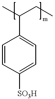
Next, on the hole injection/transport layer 3, a solution of a fluorene-based polymer having a structure shown below dissolved in a xylene solvent was applied by spin coating so as to have a film thickness of 800 angstroms, thereby forming a light-emitting layer 4.
Figure US06853130-20050208-C00004
Subsequently, on the light-emitting layer 4, first, a film formation (deposition) of Ca was performed in a vacuum deposition apparatus so as to form a first cathode 5. The vacuum deposition apparatus disposed in the closed container was used. The degree of vacuum at the beginning was approximately 1×10⁻⁶ torr. The deposition rate was set to be 3 angstroms/sec, and the film thickness was set to be 70 angstroms. Next, after the degree of vacuum again reaches 1×10⁻⁶ torr, a film 10 having angstroms thick was formed as the second cathode 6 by depositing A1 at a deposition rate of 3 angstroms/sec.
Next, on the second cathode 6, as a first sealing layer 7, a film having 500 angstroms thick was formed by depositing LiF at a deposition rate of 8 angstroms/sec.
After cooling, on the first sealing layer 7, DPpure60 (manufactured by 3M) was applied (film thickness, 200 μm) which was a moisture-proof epoxy resin, thereby forming a second sealing layer 8. A sealing glass (thickness, 0.3 mm) was then adhered thereto as a sealing substrate 9, and compressing was performed by a hot plate under conditions, at 50° C. for 12 hours, whereby curing was performed. In this step, in order to remove air bubbles in the epoxy resin, heating was performed at a degree of vacuum of approximately 0.1 torr. As a result, an organic EL device was obtained.
For the organic EL device thus obtained, the transmittance and the threshold voltage were measured. The measurement of the transmittance was performed by using a spectroscope (manufactured by Hitachi, Ltd.), in which air was used as the base line, and a pinhole of 3 mm in diameter was provided at a condenser portion. The measurement of the threshold voltage was performed using BM-7 (manufactured by Kabushiki Kaisha Topcon), and the threshold voltage was defined by a voltage at which a luminance of 5 Cd/m2 is output.
The results are shown in FIG. 2.
According to the results shown in FIG. 2, it was understood that the transmittance was 50% or more over almost the entire visible light region. In consideration of the glass substrate 1 having a thickness of 1.1 mm, and the transmittance thereof being approximately 75%, it was believed that a transmittance of 70% or more was achieved. In the case described above, the threshold voltage was 3 V.
Example 2
In accordance with the method described in Example 1, glass substrates, each having an anode stacked thereon, were obtained, wherein the anodes formed of transparent electrodes were processed by an oxygen plasma treatment for from 0 to 10 minutes at one-minute intervals. For glass substrates having anodes thereon, which were processed for 0, 5 (Example), and 10 minutes, transmission spectrums (transmittance at each wavelength) were measured. The results are shown in FIG. 3. In addition, for the glass substrates having anodes thereon, which were processed for from 0 to 10 minutes at one-minute intervals, transmittances at 450 nm, 550 nm, and 700 nm were measured. The results are shown in Table 1.
TABLE 1
Time for
an Oxygen
Plasma
Treatment 1 2 3 4 5 6 7 8 9 10
0 (min) (min) (min) (min) (min) (min) (min) (min) (min) (min) (min)
Transmittance 75.2 75.8 76.3 77 77.5 78.2 78.3 78.2 78.1 78.2 78.1
(%; at 450 nm)
Transmittance 74.6 74.7 74.9 75 75.2 75.2 75.3 75 74.8 74.5 74.3
(%; at 550 nm)
Transmittance 75.8 75.7 75.5 75.5 75.3 75.2 75 74.9 74.6 74.4 74.3
(%; at 700 nm)
In the blue region (450 nm), an increase in transmittance was observed until 5 minutes elapse from the start of the treatment. In the green region (550 nm), even though a significant change was not observed, the transmittance exhibited the maximum value approximately 5 minutes after the start of the treatment. In the red region (700 nm), as the treatment time elapsed, the transmittance was decreased even though this decrease was not significant. It is believed that the phenomenon described above occurred by a change of the band structure, since the material was partly changed due to the oxidation of the surface thereof by the treatment. Accordingly, it was considered that a treatment time of approximately 5 minutes was an optimum condition.
Example 3
Organic EL devices were formed in a manner similar to that in Example 1, except that the first cathodes were formed so as to have thicknesses of 40, 50, 60, 80, 90, and 100 angstroms. The threshold voltages and the transmittances at a wavelength of 550 nm were measured for the individual organic EL devices. In Table 2, the results of the threshold voltages and the transmittances (a wavelength region of 550 nun) are shown together with the results of Example 1 (the first cathode having a film thickness of 70 angstroms).
TABLE 2
Film Thickness
of First
Cathode
50 60 70 80 90 100
40 (Å) (Å) (Å) (Å) (Å) (Å) (Å)
Threshold 5 3.5 3.5 3 2.9 2.9 2.9
voltage (V)
Transmittance 61 59 56 54 50 45 38
(%, at 550 nm)
Concerning the threshold voltage, it was asymptomatically stabilized at a film thickness of the first cathode of approximately 70 angstroms. An increase in threshold voltage was observed when the film thickness was not more than 70 angstroms. It is believed that the phenomenon described above occurred by an increase in resistance caused by the influence of the work function of the second cathode, or by the insufficient film thickness of the second cathode.
The transmittance was decreased with the change in film thickness of the first cathode, the acceptable level was up to approximately 90 angstroms (a total thickness of the first and the second cathodes of 100 angstroms), and at a level of the thickness of the first cathode higher than that mentioned above (a level higher than that of a total thickness of the first and the second cathodes of 100 angstroms), the transmittance was excessively decreased. According to the results described above, it was believed that a film thickness of approximately 70 angstroms of the first cathode was an optimum value.
Example 4
Organic EL devices were formed in a manner similar to that in Example 1, except that the second cathodes were formed so as to have thicknesses of 5, 15, 20, 25, and 40 angstroms. The threshold voltages and the transmittances at a wavelength of 550 nm were measured for the individual organic EL devices. In Table 3, the results of the threshold voltages and the transmittances are shown together with the results of Example 1 (the second cathode having a film thickness of 10 angstroms).
TABLE 3
Film Thickness of 10 15 20 40
Second Cathode 5 (Å) (Å) (Å) (Å) (Å) (Å)
Threshold voltage (V) No Light Emission 3 3.1 3 3 3
Transmittance (%, at 57 54 49 43 32 20
550 nm)
Concerning the threshold voltage, when the thickness thereof was 10 angstroms or more, the change could not be observed. When the thickness was 10 angstroms or less, it is believed that light emission was not performed since conductance could not be obtained. Since a constant value was obtained, it was believed that there was no influence of the work function of the second cathode. A decrease in transmittance was significant compared to the case in which Ca was used. It is believed that the phenomenon was caused by A1, which had high conductivity and high reflectance.
As has been thus described in detail, according to the present invention, the transmittance in the visible region is enhanced, sealing defects are reduced, and the influence of oxygen, water, and the like in the outside air can be minimized as much as possible. In addition, as a transmissive type organic EL device, a device can be realized which has a long life, is driven at a low voltage, and has a high transmittance in the visible light region.

Claims (8)

1. An organic electroluminescent device, comprising:
a substrate;
an anode;
a light-emitting layer formed of an organic material; and
a cathode including a first cathode formed of a material having a work function of 3.0 eV or less and a second cathode formed of a material having a work function higher than the work function of the first cathode, the first and second cathodes being sequentially stacked in this order from the side of the light-emitting layer, a total thickness of the first and the second cathodes being 100 angstroms or less, and light being emitted to an exterior of the device via at least the cathode, the thickness y (angstrom) of the first cathode being such that 55≦y≦65, the thickness z (angstrom) of the second cathode being such that 10≦z≦20.
2. The organic electroluminescent device according to claim 1, the device at the cathode being sealed by a sealing layer formed of a light transmissive material.
3. The organic electroluminescent device according to claim 1, the first cathode including Ca.
4. The organic electroluminescent device according to claim 1, the second cathode including A1.
5. The organic electroluminescent device according to claim 1, the organic material forming the light-emitting layer being a polymeric material.
6. The organic electroluminescent device according to claim 1, the first cathode including Au.
7. The organic electroluminescent device according to claim 2, the sealing layer including Au.
8. The organic electroluminescent device according to claim 2, a thickness of the sealing layer including LiF being more than 300 angstrom and less than 500 angstrom.
US09/810,233 2000-03-21 2001-03-19 Organic electroluminescent device and manufacturing method therefor Expired - Lifetime US6853130B2 (en)

Priority Applications (1)

Application Number Priority Date Filing Date Title
US10/902,176 US7138762B2 (en) 2000-03-21 2004-07-30 Organic electroluminescent device and manufacturing method therefor

Applications Claiming Priority (2)

Application Number Priority Date Filing Date Title
JP2000078664 2000-03-21
JP2000-078664 2000-03-21

Related Child Applications (1)

Application Number Title Priority Date Filing Date
US10/902,176 Division US7138762B2 (en) 2000-03-21 2004-07-30 Organic electroluminescent device and manufacturing method therefor

Publications (2)

Publication Number Publication Date
US20020039730A1 US20020039730A1 (en) 2002-04-04
US6853130B2 true US6853130B2 (en) 2005-02-08

Family

ID=18596046

Family Applications (2)

Application Number Title Priority Date Filing Date
US09/810,233 Expired - Lifetime US6853130B2 (en) 2000-03-21 2001-03-19 Organic electroluminescent device and manufacturing method therefor
US10/902,176 Expired - Lifetime US7138762B2 (en) 2000-03-21 2004-07-30 Organic electroluminescent device and manufacturing method therefor

Family Applications After (1)

Application Number Title Priority Date Filing Date
US10/902,176 Expired - Lifetime US7138762B2 (en) 2000-03-21 2004-07-30 Organic electroluminescent device and manufacturing method therefor

Country Status (1)

Country Link
US (2) US6853130B2 (en)

Cited By (10)

* Cited by examiner, † Cited by third party
Publication number Priority date Publication date Assignee Title
US20030201716A1 (en) * 2002-04-26 2003-10-30 Semiconductor Energy Laboratory Co., Ltd. Light emitting device and manufacturing method of the same
US20030227021A1 (en) * 2002-06-07 2003-12-11 Semiconductor Energy Laboratory Co., Ltd. Light emitting device and manufacturing method thereof
US20040008252A1 (en) * 2002-07-09 2004-01-15 Mitsuaki Osame Method for deciding duty factor in driving light-emitting device and driving method using the duty factor
US20040189186A1 (en) * 2002-09-24 2004-09-30 Toshitaka Mori Display element and method for producing the same
US20050073243A1 (en) * 2002-06-27 2005-04-07 Semiconductor Energy Laboratory Co., Ltd. Light emitting device and method of manufacturing the same
US20070040492A1 (en) * 2003-01-10 2007-02-22 Semiconductor Energy Laboratory Co., Ltd. Method For Manufacturing Light-Emitting Device
US7554128B2 (en) 2002-12-27 2009-06-30 Semiconductor Energy Laboratory Co., Ltd. Light-emitting apparatus
US20090289548A1 (en) * 2002-12-13 2009-11-26 Semiconductor Energy Laboratory Co., Ltd. Manufacturing method of light emitting device and manufacturing device thereof
US20100181592A1 (en) * 2002-04-24 2010-07-22 Semiconductor Energy Laboratory Co., Ltd. Semiconductor Device and Method of Manufacturing Same
US20100230669A1 (en) * 2002-01-25 2010-09-16 Semiconductor Energy Laboratory Co., Ltd. Display Device and Method for Manufacturing Thereof

Families Citing this family (4)

* Cited by examiner, † Cited by third party
Publication number Priority date Publication date Assignee Title
US7579771B2 (en) 2002-04-23 2009-08-25 Semiconductor Energy Laboratory Co., Ltd. Light emitting device and method of manufacturing the same
JP4240276B2 (en) 2002-07-05 2009-03-18 株式会社半導体エネルギー研究所 Light emitting device
JP2004200141A (en) * 2002-10-24 2004-07-15 Toyota Industries Corp Organic el element
US7202504B2 (en) 2004-05-20 2007-04-10 Semiconductor Energy Laboratory Co., Ltd. Light-emitting element and display device

Citations (3)

* Cited by examiner, † Cited by third party
Publication number Priority date Publication date Assignee Title
US5739545A (en) * 1997-02-04 1998-04-14 International Business Machines Corporation Organic light emitting diodes having transparent cathode structures
US6023073A (en) * 1995-11-28 2000-02-08 International Business Machines Corp. Organic/inorganic alloys used to improve organic electroluminescent devices
US6252253B1 (en) * 1998-06-10 2001-06-26 Agere Systems Optoelectronics Guardian Corp. Patterned light emitting diode devices

Family Cites Families (4)

* Cited by examiner, † Cited by third party
Publication number Priority date Publication date Assignee Title
JPS63105493A (en) * 1986-10-22 1988-05-10 アルプス電気株式会社 Thin film el panel
US5652067A (en) * 1992-09-10 1997-07-29 Toppan Printing Co., Ltd. Organic electroluminescent device
US5962962A (en) * 1994-09-08 1999-10-05 Idemitsu Kosan Co., Ltd. Method of encapsulating organic electroluminescence device and organic electroluminescence device
JP2001338755A (en) * 2000-03-21 2001-12-07 Seiko Epson Corp Organic el element and its manufacturing method

Patent Citations (3)

* Cited by examiner, † Cited by third party
Publication number Priority date Publication date Assignee Title
US6023073A (en) * 1995-11-28 2000-02-08 International Business Machines Corp. Organic/inorganic alloys used to improve organic electroluminescent devices
US5739545A (en) * 1997-02-04 1998-04-14 International Business Machines Corporation Organic light emitting diodes having transparent cathode structures
US6252253B1 (en) * 1998-06-10 2001-06-26 Agere Systems Optoelectronics Guardian Corp. Patterned light emitting diode devices

Non-Patent Citations (1)

* Cited by examiner, † Cited by third party
Title
Gu, G. et al., "Transparent organic light emitting devices", Appl. Phys. Lett., vol. 68, No. 19, May 6, 1996, pp. 2606-2608.

Cited By (45)

* Cited by examiner, † Cited by third party
Publication number Priority date Publication date Assignee Title
US20100230669A1 (en) * 2002-01-25 2010-09-16 Semiconductor Energy Laboratory Co., Ltd. Display Device and Method for Manufacturing Thereof
US8747178B2 (en) 2002-01-25 2014-06-10 Semiconductor Energy Laboratory Co., Ltd. Manufacturing method of light emitting device
US8937429B2 (en) 2002-01-25 2015-01-20 Semiconductor Energy Laboratory Co., Ltd. Display device and method for manufacturing thereof
US8450925B2 (en) 2002-01-25 2013-05-28 Semiconductor Energy Laboratory Co., Ltd. Display device and method for manufacturing thereof
US8004183B2 (en) 2002-01-25 2011-08-23 Semiconductor Energy Laboratory Co., Ltd. Display device and method for manufacturing thereof
US8624235B2 (en) 2002-04-24 2014-01-07 Semiconductor Energy Laboratory Co., Ltd. Semiconductor device and method of manufacturing same
US9362534B2 (en) 2002-04-24 2016-06-07 Semiconductor Energy Laboratory Co., Ltd. Semiconductor device and method of manufacturing same
US9000429B2 (en) 2002-04-24 2015-04-07 Semiconductor Energy Laboratory Co., Ltd. Semiconductor device and method of manufacturing same
US8785919B2 (en) 2002-04-24 2014-07-22 Semiconductor Energy Laboratory Co., Ltd. Semiconductor device and method of manufacturing same
US9831459B2 (en) 2002-04-24 2017-11-28 Semiconductor Energy Laboratory Co., Ltd. Display module with white light
US8344363B2 (en) 2002-04-24 2013-01-01 Semiconductor Energy Laboratory Co., Ltd. Semiconductor device and method of manufacturing same
US10454059B2 (en) 2002-04-24 2019-10-22 Semiconductor Energy Laboratory Co., Ltd. Semiconductor device and method of manufacturing same
US9165987B2 (en) 2002-04-24 2015-10-20 Semiconductor Energy Laboratory Co., Ltd. Semiconductor device and method of manufacturing same
US20100181592A1 (en) * 2002-04-24 2010-07-22 Semiconductor Energy Laboratory Co., Ltd. Semiconductor Device and Method of Manufacturing Same
US7402948B2 (en) 2002-04-26 2008-07-22 Semiconductor Energy Laboratory Co., Ltd. Light emitting device
US20030201716A1 (en) * 2002-04-26 2003-10-30 Semiconductor Energy Laboratory Co., Ltd. Light emitting device and manufacturing method of the same
US9853098B2 (en) 2002-04-26 2017-12-26 Semiconductor Energy Laboratory Co., Ltd. Light emitting device and manufacturing method of the same
US8497628B2 (en) 2002-04-26 2013-07-30 Semiconductor Energy Laboratory Co., Ltd. Light emitting device and manufacturing method of the same
US9412804B2 (en) 2002-04-26 2016-08-09 Semiconductor Energy Laboratory Co., Ltd. Light emitting device and manufacturing method of the same
US20080252207A1 (en) * 2002-04-26 2008-10-16 Semiconductor Energy Laboratory Co., Ltd. Light emitting device and manufacturing method of the same
US8044580B2 (en) 2002-04-26 2011-10-25 Semiconductor Energy Laboratory Co., Ltd. Light emitting device and manufacturing method of the same
US8803418B2 (en) 2002-04-26 2014-08-12 Semiconductor Energy Laboratory Co., Ltd. Light emitting device and manufacturing method of the same
US8309976B2 (en) 2002-06-07 2012-11-13 Semiconductor Energy Laboratory Co., Ltd. Light emitting device and manufacturing method thereof
US7897979B2 (en) 2002-06-07 2011-03-01 Semiconductor Energy Laboratory Co., Ltd. Light emitting device and manufacturing method thereof
US20030227021A1 (en) * 2002-06-07 2003-12-11 Semiconductor Energy Laboratory Co., Ltd. Light emitting device and manufacturing method thereof
US9166202B2 (en) 2002-06-07 2015-10-20 Semiconductor Energy Laboratory Co., Ltd. Light emitting device and manufacturing method thereof
US8704243B2 (en) 2002-06-07 2014-04-22 Semiconductor Energy Laboratory Co., Ltd. Light emitting device and manufacturing method thereof
US20110193070A1 (en) * 2002-06-07 2011-08-11 Semiconductor Energy Laboratory Co., Ltd. Light Emitting Device and Manufacturing Method Thereof
US8540541B2 (en) 2002-06-27 2013-09-24 Semiconductor Energy Laboratory Co., Ltd. Light emitting device and method of manufacturing the same
US20100221855A1 (en) * 2002-06-27 2010-09-02 Semiconductor Energy Laboratory Co., Ltd. Light Emitting Device and Method of Manufacturing the Same
US7663305B2 (en) 2002-06-27 2010-02-16 Semiconductor Energy Laboratory Co., Ltd. Light emitting device and method of manufacturing the same
US20050073243A1 (en) * 2002-06-27 2005-04-07 Semiconductor Energy Laboratory Co., Ltd. Light emitting device and method of manufacturing the same
US20040008252A1 (en) * 2002-07-09 2004-01-15 Mitsuaki Osame Method for deciding duty factor in driving light-emitting device and driving method using the duty factor
US9153168B2 (en) 2002-07-09 2015-10-06 Semiconductor Energy Laboratory Co., Ltd. Method for deciding duty factor in driving light-emitting device and driving method using the duty factor
US7161291B2 (en) * 2002-09-24 2007-01-09 Dai Nippon Printing Co., Ltd Display element and method for producing the same
US20040189186A1 (en) * 2002-09-24 2004-09-30 Toshitaka Mori Display element and method for producing the same
US20070048437A1 (en) * 2002-09-24 2007-03-01 Junji Kido Display element and method for producing the same
US9379351B2 (en) 2002-09-24 2016-06-28 Dai Nippon Printing Co., Ltd. Display element and method for producing the same
US20090289548A1 (en) * 2002-12-13 2009-11-26 Semiconductor Energy Laboratory Co., Ltd. Manufacturing method of light emitting device and manufacturing device thereof
US8482011B2 (en) 2002-12-13 2013-07-09 Semiconductor Energy Laboratory Co., Ltd. Light-emitting device
US8237176B2 (en) 2002-12-13 2012-08-07 Semiconductor Energy Laboratory Co., Ltd. Light emitting device
US8044411B2 (en) 2002-12-13 2011-10-25 Semiconductor Energy Laboratory Co., Ltd. Light emitting device
US7554128B2 (en) 2002-12-27 2009-06-30 Semiconductor Energy Laboratory Co., Ltd. Light-emitting apparatus
US20070040492A1 (en) * 2003-01-10 2007-02-22 Semiconductor Energy Laboratory Co., Ltd. Method For Manufacturing Light-Emitting Device
US8492968B2 (en) 2003-01-10 2013-07-23 Semiconductor Energy Laboratory Co., Ltd. Method for manufacturing light-emitting device

Also Published As

Publication number Publication date
US7138762B2 (en) 2006-11-21
US20050023968A1 (en) 2005-02-03
US20020039730A1 (en) 2002-04-04

Similar Documents

Publication Publication Date Title
KR100441415B1 (en) Opto-electrical devices
US6617052B2 (en) Organic EL element and method of manufacturing the same
JP4628104B2 (en) Light emitting device and manufacturing method thereof
US7629018B2 (en) Light emitting device and method of manufacturing the same
TWI389594B (en) Stacked organic electroluminescent devices
US8558453B2 (en) Active matrix display device
US7161295B2 (en) Display device with cathode containing lithium
US6853130B2 (en) Organic electroluminescent device and manufacturing method therefor
JP4651916B2 (en) Method for manufacturing light emitting device
TW201220921A (en) Light emitting device, electronic equipment and apparatus for manufacturing the same
JP2005197210A (en) Organic light emitting device and its manufacturing method
JP3963712B2 (en) Organic EL element structure
US20040178725A1 (en) Display panel, electronic apparatus with the same, and method of manufacturing the same
US9012896B2 (en) Organic EL element
JP3953404B2 (en) ORGANIC ELECTROLUMINESCENCE ELEMENT, METHOD FOR PRODUCING THE ORGANIC ELECTROLUMINESCENCE ELEMENT, AND ORGANIC ELECTROLUMINESCENCE DISPLAY DEVICE
JP4810739B2 (en) Organic electroluminescence device and method for producing the same
US7112113B2 (en) Manufacturing method of display device
US20060202610A1 (en) Display panel, electronic apparatus with the same, and method of manufacturing the same
US7429822B2 (en) Organic electroluminescence device having a cathode with a metal layer that includes a first metal and a low work function metal
KR100615221B1 (en) An organic electro luminescent display device and a method for preparing the same
JP4133736B2 (en) Organic EL device
JP2001351779A (en) Manufacturing method of organic el element, and the organic el element
JP5678455B2 (en) Method for manufacturing organic EL element and method for manufacturing organic EL panel
JP2000348865A (en) Organic electroluminescent element
KR20050114204A (en) Multi-pixel display devices and method for forming the same

Legal Events

Date Code Title Description
AS Assignment

Owner name: SEIKO EPSON CORPORATION, JAPAN

Free format text: ASSIGNMENT OF ASSIGNORS INTEREST;ASSIGNOR:MORII, KATSUYUKI;REEL/FRAME:012023/0507

Effective date: 20010730

STCF Information on status: patent grant

Free format text: PATENTED CASE

FPAY Fee payment

Year of fee payment: 4

FEPP Fee payment procedure

Free format text: PAYOR NUMBER ASSIGNED (ORIGINAL EVENT CODE: ASPN); ENTITY STATUS OF PATENT OWNER: LARGE ENTITY

Free format text: PAYER NUMBER DE-ASSIGNED (ORIGINAL EVENT CODE: RMPN); ENTITY STATUS OF PATENT OWNER: LARGE ENTITY

FPAY Fee payment

Year of fee payment: 8

FPAY Fee payment

Year of fee payment: 12