US6855638B2 - Process to pattern thick TiW metal layers using uniform and selective etching - Google Patents
Process to pattern thick TiW metal layers using uniform and selective etching Download PDFInfo
- Publication number
- US6855638B2 US6855638B2 US10/396,168 US39616803A US6855638B2 US 6855638 B2 US6855638 B2 US 6855638B2 US 39616803 A US39616803 A US 39616803A US 6855638 B2 US6855638 B2 US 6855638B2
- Authority
- US
- United States
- Prior art keywords
- metal layer
- tiw metal
- tiw
- etched
- layer portion
- Prior art date
- Legal status (The legal status is an assumption and is not a legal conclusion. Google has not performed a legal analysis and makes no representation as to the accuracy of the status listed.)
- Expired - Fee Related
Links
Images


Classifications
-
- C—CHEMISTRY; METALLURGY
- C23—COATING METALLIC MATERIAL; COATING MATERIAL WITH METALLIC MATERIAL; CHEMICAL SURFACE TREATMENT; DIFFUSION TREATMENT OF METALLIC MATERIAL; COATING BY VACUUM EVAPORATION, BY SPUTTERING, BY ION IMPLANTATION OR BY CHEMICAL VAPOUR DEPOSITION, IN GENERAL; INHIBITING CORROSION OF METALLIC MATERIAL OR INCRUSTATION IN GENERAL
- C23F—NON-MECHANICAL REMOVAL OF METALLIC MATERIAL FROM SURFACE; INHIBITING CORROSION OF METALLIC MATERIAL OR INCRUSTATION IN GENERAL; MULTI-STEP PROCESSES FOR SURFACE TREATMENT OF METALLIC MATERIAL INVOLVING AT LEAST ONE PROCESS PROVIDED FOR IN CLASS C23 AND AT LEAST ONE PROCESS COVERED BY SUBCLASS C21D OR C22F OR CLASS C25
- C23F4/00—Processes for removing metallic material from surfaces, not provided for in group C23F1/00 or C23F3/00
-
- H—ELECTRICITY
- H01—ELECTRIC ELEMENTS
- H01L—SEMICONDUCTOR DEVICES NOT COVERED BY CLASS H10
- H01L21/00—Processes or apparatus adapted for the manufacture or treatment of semiconductor or solid state devices or of parts thereof
- H01L21/02—Manufacture or treatment of semiconductor devices or of parts thereof
- H01L21/04—Manufacture or treatment of semiconductor devices or of parts thereof the devices having at least one potential-jump barrier or surface barrier, e.g. PN junction, depletion layer or carrier concentration layer
- H01L21/18—Manufacture or treatment of semiconductor devices or of parts thereof the devices having at least one potential-jump barrier or surface barrier, e.g. PN junction, depletion layer or carrier concentration layer the devices having semiconductor bodies comprising elements of Group IV of the Periodic System or AIIIBV compounds with or without impurities, e.g. doping materials
- H01L21/30—Treatment of semiconductor bodies using processes or apparatus not provided for in groups H01L21/20 - H01L21/26
- H01L21/31—Treatment of semiconductor bodies using processes or apparatus not provided for in groups H01L21/20 - H01L21/26 to form insulating layers thereon, e.g. for masking or by using photolithographic techniques; After treatment of these layers; Selection of materials for these layers
- H01L21/3205—Deposition of non-insulating-, e.g. conductive- or resistive-, layers on insulating layers; After-treatment of these layers
- H01L21/321—After treatment
- H01L21/3213—Physical or chemical etching of the layers, e.g. to produce a patterned layer from a pre-deposited extensive layer
- H01L21/32133—Physical or chemical etching of the layers, e.g. to produce a patterned layer from a pre-deposited extensive layer by chemical means only
- H01L21/32135—Physical or chemical etching of the layers, e.g. to produce a patterned layer from a pre-deposited extensive layer by chemical means only by vapour etching only
- H01L21/32136—Physical or chemical etching of the layers, e.g. to produce a patterned layer from a pre-deposited extensive layer by chemical means only by vapour etching only using plasmas
-
- H—ELECTRICITY
- H01—ELECTRIC ELEMENTS
- H01F—MAGNETS; INDUCTANCES; TRANSFORMERS; SELECTION OF MATERIALS FOR THEIR MAGNETIC PROPERTIES
- H01F41/00—Apparatus or processes specially adapted for manufacturing or assembling magnets, inductances or transformers; Apparatus or processes specially adapted for manufacturing materials characterised by their magnetic properties
- H01F41/32—Apparatus or processes specially adapted for manufacturing or assembling magnets, inductances or transformers; Apparatus or processes specially adapted for manufacturing materials characterised by their magnetic properties for applying conductive, insulating or magnetic material on a magnetic film, specially adapted for a thin magnetic film
- H01F41/34—Apparatus or processes specially adapted for manufacturing or assembling magnets, inductances or transformers; Apparatus or processes specially adapted for manufacturing materials characterised by their magnetic properties for applying conductive, insulating or magnetic material on a magnetic film, specially adapted for a thin magnetic film in patterns, e.g. by lithography
Definitions
- This invention relates to the field of semiconductor manufacture, and more particularly to uniform patterning of titanium tungsten (TiW) greater than two thousand angstroms in thickness with selectivity to the underlying dielectric material.
- the manufacture of semiconductors involves the patterning of semiconductor, dielectric and metallic films. This is accomplished by transferring a patterned photoresist or other masking layer to the desired film layer. This pattern transfer is typically accomplished using a plasma etch process.
- the present invention solves these needs and other problems in the field of TiW metal layer manufacturing methods by providing, in most preferred aspects, a method including: providing a substrate; depositing a dielectric layer on the substrate; depositing an at least 2000 angstrom thick TiW metal layer onto the dielectric layer; depositing a photoresist over the at least 2000 angstrom thick TiW metal layer; uniformly etching the at least 2000 angstrom thick TiW metal layer to form an etched TiW metal layer portion; and selectively etching the etched TiW metal layer portion faster than the dielectric layer creating a uniformly patterned TiW metal layer.
- the method provides the substrate in the form of a semiconductor substrate.
- the method uniformly etches the at least 2000 angstrom thick TiW metal layer to form an etched TiW metal layer portion that is at least 200 angstroms thick.
- the method uniformly etches no more than 80% to 90% of the at least 2000 angstrom thick TiW metal layer to form the etched TiW metal layer portion.
- the method etches the at least 2000 angstrom thick TiW metal layer by processing in a Lam 9606 reactor with the following process settings:
- Ar 32 sccm (standard cubic centimeters per minute)
- BCl3 24 sccm (standard cubic centimeters per minute)
- SF6 24 sccm (standard cubic centimeters per minute)
- Total flow 80 sccm (standard cubic centimeters per minute)
- Gap 3 cm (centimeter)
- Clamp pressure 5 T (Torricelli)
- Electrode temperature 60° C.
- the method selectively etches the etched TiW metal layer portion at least 2.7 times faster than the dielectric layer.
- the method selectively etches the etched TiW metal layer portion to remove the etched TiW metal layer portion.
- the method selectively etches the etched TiW metal layer portion by processing in a Lam 9606 reactor with the following process settings:
- Top Power 600 Watts
- Ar 0 sccm (standard cubic centimeters per minute)
- BCl3 80 sccm (standard cubic centimeters per minute)
- SF6 10 sccm (standard cubic centimeters per minute)
- Total flow 90 sccm (standard cubic centimeters per minute)
- Gap 3 cm (centimeter)
- Clamp pressure 5 T (Torricelli)
- Electrode temperature 60° C.
- the method deposits an at least 2000 angstrom thick TiW metal layer in the form of an at least 2000 angstrom thick TiW metal film onto the dielectric layer.
- the method deposits an at least 2000 angstrom thick TiW metal layer in the form of an at least 3000 angstrom thick TiW metal film onto the dielectric layer.
- the method deposits a dielectric layer of silicon nitride on the substrate.
- the method deposits a dielectric layer of silicon dioxide on the substrate.
- FIG. 1 shows a TiW layer deposited on a substrate and a photoresist layer deposited on the TiW layer according to the preferred teachings of the present invention.
- FIG. 2 shows a partially formed structure in a TiW layer on a substrate according to the preferred teachings of the present invention.
- FIG. 3 shows a fully formed structure on a TiW layer in a substrate according to the preferred teachings of the present invention.
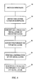
- FIG. 4 shows a method, according to the preferred teachings of the present invention, of creating a fully formed structure in a TiW layer on a substrate.
- FIG. 4 diagrammatically shows a process for patterning TiW metal layer 12 uniformly with a thickness greater than two thousand angstroms and with selectivity to a dielectric layer 15 .
- the dielectric layer 15 can be an underlying semiconductor substrate with a dielectric layer.
- the methods of the present invention are useful for creating microelectronic devices in the semiconductor.
- a substrate 14 is provided as diagrammatically indicated by box 16 .
- the substrate 14 is a semiconductor substrate made from a semiconductor such as silicon.
- the processes according to the preferred teachings of the present invention are useful in the formation of electromigration resistant electronic circuits.
- underlying circuitry is fabricated using conventional methods and processes, employing one or more layers of conventional interconnects to produce a partially connected and partially functional front-end.
- the upper layer of the front-end is a material of a thickness sufficient for the designed purpose of the circuit.
- the front-end is then used as the substrate 14 , also having a dielectric layer, on which the specialized circuitry is fabricated.
- the dielectric layer 15 is deposited on the substrate 14 as diagrammatically indicated by box 18 .
- the dielectric layer 15 may be a silicon nitride layer.
- silicon dioxide may be used without deviating from the spirit and scope of the present invention.
- the TiW metal layer 12 which according to the preferred teachings of the present invention is 2000 angstroms or greater, 3000 angstroms typical, is deposited on the dielectric layer 15 in a well known manner as is diagrammatically illustrated by box 20 .
- a photoresist 10 is then deposited on the TiW metal layer 12 in a well-known manner as is diagrammatically illustrated by box 22 .
- the photoresist 10 is a standard photoresist, such as a low contrast or high contrast photoresist such as AZ3312 and AZ7908 available from AZ Electronic Materials of Sommerville, N.J. These example photoresists are given by way of example, and not limitation, and those skilled in the art will recognize that other suitable photoresists may be used without deviating from the spirit and scope of the present invention.
- Photoresist 10 is deposited over the TiW metal layer 12 and patterned using conventional photolithographic techniques.
- the TiW metal layer 12 is a TiW metal film.
- a uniform etch of the TiW metal layer 12 is then performed as is diagrammatically illustrated by box 24 .
- the TiW metal layer 12 is etched using a uniform process until most of the TiW metal layer 12 has been removed but the underlying dielectric layer 15 is not yet exposed to the plasma etch.
- the uniform etch forms a TiW metal layer portion 17 and TiW metal layer portion 19 .
- the uniform etch of the TiW metal layer 12 is a uniform plasma etch.
- no more than 80% to 90% of the TiW metal layer 12 is etched by the uniform etching to form the TiW metal layer portion 17 and TiW metal layer portion 19 .
- a 2000 angstrom thick TiW metal layer 12 etches down to form 400 to 200 angstrom thick TiW metal layer portions 17 and 19 .
- the main etch process was performed in a Lam 9606 reactor, available from LAM Research, Inc, with the following process settings:
- Ar 32 sccm (standard cubic centimeters/per minute)
- BCl3 24 sccm (standard cubic centimeters/per minute)
- SF6 24 sccm (standard cubic centimeters/per minute)
- Total flow 80 sccm (standard cubic centimeters/per minute)
- Gap 3 cm (centimeter)
- Clamp pressure 5 T (Torricelli)
- Electrode temperature 60° C.
- the remaining TiW metal layer 12 is etched with a highly selective overetch to uniformly pattern the TiW metal layer 12 as is diagrammatically illustrated by box 26 .
- the selective etch is performed in the Lam 9606 reactor with a process that etches the TiW metal layer 12 selectively to the dielectric layer 15 to remove the remaining TiW metal layer 12 not covered by the photoresist 10 .
- the selective etch selectively etches the uniformly etched TiW metal layer 12 at least 2.7 times faster than the dielectric layer 15 creating the uniformly patterned TiW metal layer 12 .
- BCL3, boron trichloride, and SF6, sulfur hexafluoride are used to etch the TiW metal layer 12 faster than the dielectric layer 15 .
- the uniform etch etches the TiW metal layer 12 to a certain uniformity but does not break into the dielectric layer 15 .
- the selective etch because it etches the TiW metal layer 12 faster than the dielectric layer 15 , allows the completion of the patterned TiW metal layer 12 by breaking through to the dielectric layer 15 while at the same time reducing the transfer of nonuniformity to the dielectric layer 15 .
- the reduction in transfer of the nonuniformity is directly related to the selective etch rate.
- nonuniformity in the TiW metal layer 12 will be reduced 2.7 times in the dielectric layer 15 , thereby allowing for a uniformly patterned TiW metal layer 12 .
- By not transferring nonuniformity to the dielectric layer 15 prevents shorting and exposure of underlying material to plasma that may be detrimental and creates devices that perform better with a process with higher yield.
- the selective etch process performs an overetch and is performed in the Lam 9606 reactor with the following process settings:
- Top Power 600 Watts
- Ar 0 sccm (standard cubic centimeters per minute)
- BCl3 80 sccm (standard cubic centimeters per minute)
- SF6 10 sccm (standard cubic centimeters per minute)
- Total flow 90 sccm (standard cubic centimeters per minute)
- Gap 3 cm (centimeter)
- Clamp pressure 5 T (Torricelli)
- Electrode temperature 60° C.
- TiW ER is the TiW etch rate.
- TiW U(3sig.) is the TiW non-uniformity.
- PR ER is the photoresist etch rate.
- PR U(3sig.) is the photoresist non-uniformity.
- SiN ER is the SiN etch rate.
- TiW:PR is the selectivity, as the ratio of TiW etch rate to the photoresist etch rate.
- TiW:Si is the selectivity, as the ratio of the TiW etch rate to the SiN etch rate.
Abstract
Description
| Top Power = 350 Watts | |
| Bottom Power = 93 Watts | |
| Pressure = 7 mT | (milli Torricelli) |
| Ar = 32 sccm | (standard cubic centimeters per minute) |
| BCl3 = 24 sccm | (standard cubic centimeters per minute) |
| SF6 = 24 sccm | (standard cubic centimeters per minute) |
| Total flow = 80 sccm | (standard cubic centimeters per minute) |
| Gap = 3 cm | (centimeter) |
| Clamp pressure = 5 T | (Torricelli) |
| Electrode temperature = 60° C. | |
| Top Power = 600 Watts | |
| Bottom Power = 70 Watts | |
| Pressure = 10 mT | (milli Torricelli) |
| Ar = 0 sccm | (standard cubic centimeters per minute) |
| BCl3 = 80 sccm | (standard cubic centimeters per minute) |
| SF6 = 10 sccm | (standard cubic centimeters per minute) |
| Total flow = 90 sccm | (standard cubic centimeters per minute) |
| Gap = 3 cm | (centimeter) |
| Clamp pressure = 5 T | (Torricelli) |
| Electrode temperature = 60° C. | |
| Top Power = 350 Watts | |
| Bottom Power = 93 Watts | |
| Pressure = 7 mT | (milli Torricelli) |
| Ar = 32 sccm | (standard cubic centimeters/per minute) |
| BCl3 = 24 sccm | (standard cubic centimeters/per minute) |
| SF6 = 24 sccm | (standard cubic centimeters/per minute) |
| Total flow = 80 sccm | (standard cubic centimeters/per minute) |
| Gap = 3 cm | (centimeter) |
| Clamp pressure = 5 T | (Torricelli) |
| Electrode temperature = 60° C. | |
| Top Power = 600 Watts | |
| Bottom Power = 70 Watts | |
| Pressure = 10 mT | (milliTorricelli) |
| Ar = 0 sccm | (standard cubic centimeters per minute) |
| BCl3 = 80 sccm | (standard cubic centimeters per minute) |
| SF6 = 10 sccm | (standard cubic centimeters per minute) |
| Total flow = 90 sccm | (standard cubic centimeters per minute) |
| Gap = 3 cm | (centimeter) |
| Clamp pressure = 5 T | (Torricelli) |
| Electrode temperature = 60° C. | |
| TABLE A | ||||||||||||
| Exp. | Run | Power | TiW | PR | SiN | TiW:PR | TiW:SiN | |||||
| # | # | (T/B) | Pressure | TiW ER | U(3sig.) | PR ER | U(3sig.) | SiN ER | U(3sig.) | Sel. | Sel. | |
| 1 | 4 | 520/80 | 10 | 2662 | 14.8 | 3311 | 17.7 | 2226 | 23.1 | 0.80 | 1.20 | |
| 2 | 2 | 520/80 | 7 | 2458 | 14.7 | 3089 | 16.4 | 2109 | 20.2 | 0.80 | 1.17 | |
| 3 | 5 | 350/93 | 10 | 2218 | 15.1 | 3691 | 17.1 | 2198 | 21.2 | 0.60 | 1.01 | |
| 4 | 3 | 350/93 | 7 | 2092 | 13.9 | 3448 | 13.4 | 2079 | 18.1 | 0.61 | 1.01 | Std Main Etch |
| 5 | 1 | 435/87 | 9 | 2328 | 16.5 | 3275 | 15.3 | 2082 | 20.5 | 0.71 | 1.12 | |
| Exp. | Run | Power | TiW | PR | SiN | TiW:PR | TiW:SiN | ||||||
| # | # | (T/B) | BCL3 | SF6 | TiW ER | U(3sig.) | PR ER | U(3sig.) | SiN ER | U(3sig.) | Sel. | Sel. | |
| 1 | 4 | 490/80 | 80 | 10 | 1174 | 32.7 | 1006 | 16.2 | 529 | 39.2 | 1.17 | 2.22 | |
| 2 | 2 | 600/70 | 80 | 10 | 1284 | 34.2 | 733 | 15.2 | 464 | 40.6 | 1.75 | 2.77 | Std OE |
| 3 | 5 | 490/80 | 90 | 0 | 106 | 25.2 | 373 | 43.7 | 7.5 | 4308 | 0.28 | 14.1 | |
| 4 | 3 | 600/70 | 90 | 0 | 1232 | 33.6 | 664 | 13.4 | 460 | 38.5 | 1.86 | 2.68 | |
| 5 | 1 | 545/75 | 85 | 10 | 1248 | 35.1 | 844 | 14.6 | 492 | 37.1 | 1.48 | 2.54 | |
| Where: | |||||||||||||
| Power (T/B) is the top and bottom electrode power. | |||||||||||||
| Pressure is in Torricelli. | |||||||||||||
| TiW ER is the TiW etch rate. | |||||||||||||
| TiW U(3sig.) is the TiW non-uniformity. | |||||||||||||
| PR ER is the photoresist etch rate. | |||||||||||||
| PR U(3sig.) is the photoresist non-uniformity. | |||||||||||||
| SiN ER is the SiN etch rate. | |||||||||||||
| TiW:PR is the selectivity, as the ratio of TiW etch rate to the photoresist etch rate. | |||||||||||||
| TiW:Si is the selectivity, as the ratio of the TiW etch rate to the SiN etch rate. | |||||||||||||
| Ar is Argon | |||||||||||||
| BCL3 is boron trichloride | |||||||||||||
| SF6 is sulfur hexafluoride | |||||||||||||
Claims (20)
Priority Applications (1)
| Application Number | Priority Date | Filing Date | Title |
|---|---|---|---|
| US10/396,168 US6855638B2 (en) | 2003-03-24 | 2003-03-24 | Process to pattern thick TiW metal layers using uniform and selective etching |
Applications Claiming Priority (1)
| Application Number | Priority Date | Filing Date | Title |
|---|---|---|---|
| US10/396,168 US6855638B2 (en) | 2003-03-24 | 2003-03-24 | Process to pattern thick TiW metal layers using uniform and selective etching |
Publications (2)
| Publication Number | Publication Date |
|---|---|
| US20040192062A1 US20040192062A1 (en) | 2004-09-30 |
| US6855638B2 true US6855638B2 (en) | 2005-02-15 |
Family
ID=32988742
Family Applications (1)
| Application Number | Title | Priority Date | Filing Date |
|---|---|---|---|
| US10/396,168 Expired - Fee Related US6855638B2 (en) | 2003-03-24 | 2003-03-24 | Process to pattern thick TiW metal layers using uniform and selective etching |
Country Status (1)
| Country | Link |
|---|---|
| US (1) | US6855638B2 (en) |
Cited By (1)
| Publication number | Priority date | Publication date | Assignee | Title |
|---|---|---|---|---|
| US20060084992A1 (en) * | 1988-06-13 | 2006-04-20 | Michelson Gary K | Tubular member having a passage and opposed bone contacting extensions |
Families Citing this family (15)
| Publication number | Priority date | Publication date | Assignee | Title |
|---|---|---|---|---|
| US7799699B2 (en) | 2004-06-04 | 2010-09-21 | The Board Of Trustees Of The University Of Illinois | Printable semiconductor structures and related methods of making and assembling |
| US7521292B2 (en) | 2004-06-04 | 2009-04-21 | The Board Of Trustees Of The University Of Illinois | Stretchable form of single crystal silicon for high performance electronics on rubber substrates |
| KR101260981B1 (en) * | 2004-06-04 | 2013-05-10 | 더 보오드 오브 트러스티스 오브 더 유니버시티 오브 일리노이즈 | Methods and devices for fabricating and assembling printable semiconductor elements |
| US8217381B2 (en) | 2004-06-04 | 2012-07-10 | The Board Of Trustees Of The University Of Illinois | Controlled buckling structures in semiconductor interconnects and nanomembranes for stretchable electronics |
| US8372726B2 (en) | 2008-10-07 | 2013-02-12 | Mc10, Inc. | Methods and applications of non-planar imaging arrays |
| US8886334B2 (en) | 2008-10-07 | 2014-11-11 | Mc10, Inc. | Systems, methods, and devices using stretchable or flexible electronics for medical applications |
| US8389862B2 (en) | 2008-10-07 | 2013-03-05 | Mc10, Inc. | Extremely stretchable electronics |
| US8097926B2 (en) | 2008-10-07 | 2012-01-17 | Mc10, Inc. | Systems, methods, and devices having stretchable integrated circuitry for sensing and delivering therapy |
| US9723122B2 (en) | 2009-10-01 | 2017-08-01 | Mc10, Inc. | Protective cases with integrated electronics |
| US9765934B2 (en) | 2011-05-16 | 2017-09-19 | The Board Of Trustees Of The University Of Illinois | Thermally managed LED arrays assembled by printing |
| EP2712491B1 (en) | 2011-05-27 | 2019-12-04 | Mc10, Inc. | Flexible electronic structure |
| US9171794B2 (en) | 2012-10-09 | 2015-10-27 | Mc10, Inc. | Embedding thin chips in polymer |
| US9343661B2 (en) | 2014-02-18 | 2016-05-17 | Everspin Technologies, Inc. | Non-reactive photoresist removal and spacer layer optimization in a magnetoresistive device |
| US9466788B2 (en) * | 2014-02-18 | 2016-10-11 | Everspin Technologies, Inc. | Top electrode etch in a magnetoresistive device and devices manufactured using same |
| US9524881B2 (en) * | 2015-04-30 | 2016-12-20 | Texas Instruments Incorporated | Method for fabricating specific termination angles in titanium tungsten layers |
Citations (3)
| Publication number | Priority date | Publication date | Assignee | Title |
|---|---|---|---|---|
| US5407861A (en) * | 1992-05-27 | 1995-04-18 | Sgs-Thomson Microelectronics, S.R.L. | Metallization over tungsten plugs |
| US5607818A (en) * | 1991-06-04 | 1997-03-04 | Micron Technology, Inc. | Method for making interconnects and semiconductor structures using electrophoretic photoresist deposition |
| US5804502A (en) * | 1997-01-16 | 1998-09-08 | Vlsi Technology, Inc. | Tungsten plugs for integrated circuits and methods for making same |
-
2003
- 2003-03-24 US US10/396,168 patent/US6855638B2/en not_active Expired - Fee Related
Patent Citations (4)
| Publication number | Priority date | Publication date | Assignee | Title |
|---|---|---|---|---|
| US5607818A (en) * | 1991-06-04 | 1997-03-04 | Micron Technology, Inc. | Method for making interconnects and semiconductor structures using electrophoretic photoresist deposition |
| US5407861A (en) * | 1992-05-27 | 1995-04-18 | Sgs-Thomson Microelectronics, S.R.L. | Metallization over tungsten plugs |
| US5804502A (en) * | 1997-01-16 | 1998-09-08 | Vlsi Technology, Inc. | Tungsten plugs for integrated circuits and methods for making same |
| US5990561A (en) * | 1997-01-16 | 1999-11-23 | Vlsi Technologies, Inc. | Tungsten plugs for integrated circuits and methods for making same |
Cited By (1)
| Publication number | Priority date | Publication date | Assignee | Title |
|---|---|---|---|---|
| US20060084992A1 (en) * | 1988-06-13 | 2006-04-20 | Michelson Gary K | Tubular member having a passage and opposed bone contacting extensions |
Also Published As
| Publication number | Publication date |
|---|---|
| US20040192062A1 (en) | 2004-09-30 |
Similar Documents
| Publication | Publication Date | Title |
|---|---|---|
| US6855638B2 (en) | Process to pattern thick TiW metal layers using uniform and selective etching | |
| US5160407A (en) | Low pressure anisotropic etch process for tantalum silicide or titanium silicide layer formed over polysilicon layer deposited on silicon oxide layer on semiconductor wafer | |
| US6716761B2 (en) | Method of forming fine patterns | |
| US4412885A (en) | Materials and methods for plasma etching of aluminum and aluminum alloys | |
| US7112532B2 (en) | Process for forming a dual damascene structure | |
| US6187663B1 (en) | Method of optimizing device performance via use of copper damascene structures, and HSQ/FSG, hybrid low dielectric constant materials | |
| US6387798B1 (en) | Method of etching trenches for metallization of integrated circuit devices with a narrower width than the design mask profile | |
| EP0905768A1 (en) | A dual damascene process for metal layers and organic intermetal layers | |
| US5792672A (en) | Photoresist strip method | |
| KR20000048235A (en) | A method to optimize copper chemical-mechanical polishing in a copper damascence interconnect process for integrated circuit application | |
| TW514965B (en) | Etching method | |
| JPH0745616A (en) | Manufacture of semiconductor device | |
| US20230389436A1 (en) | Metal/Dielectric/Metal Hybrid Hard Mask To Define Ultra-Large Height Top Electrode For Sub 60nm MRAM Devices | |
| JPH1027849A (en) | Multilevel photoresist pattern transfer method | |
| US6235653B1 (en) | Ar-based si-rich oxynitride film for dual damascene and/or contact etch stop layer | |
| US6271115B1 (en) | Post metal etch photoresist strip method | |
| US6913868B2 (en) | Conductive bi-layer e-beam resist with amorphous carbon | |
| US11329218B2 (en) | Multiply spin-coated ultra-thick hybrid hard mask for sub 60nm MRAM devices | |
| US6399424B1 (en) | Method of manufacturing contact structure | |
| US6743725B1 (en) | High selectivity SiC etch in integrated circuit fabrication | |
| US5783036A (en) | Method for dry etching metal films having high melting points | |
| US6417090B1 (en) | Damascene arrangement for metal interconnection using low k dielectric constant materials for etch stop layer | |
| JP2907314B2 (en) | Method for manufacturing semiconductor device | |
| US6287752B1 (en) | Semiconductor device, method of manufacturing a semiconductor device, and method of forming a pattern for semiconductor device | |
| US6548413B1 (en) | Method to reduce microloading in metal etching |
Legal Events
| Date | Code | Title | Description |
|---|---|---|---|
| AS | Assignment |
Owner name: RIDER BENNETT, LLP, MINNESOTA Free format text: ATTORNEY'S LIEN RELEASE;ASSIGNOR:UNION SEMICONDUCTOR TECHNOLOGY CORPORATION;REEL/FRAME:014149/0364 Effective date: 20031031 |
|
| AS | Assignment |
Owner name: UNION SEMICONDUCTOR TECHNOLOGY CORPORATION, MINNES Free format text: ASSIGNMENT OF ASSIGNORS INTEREST;ASSIGNOR:MIKELSON, HANS PETER;REEL/FRAME:015790/0453 Effective date: 20040823 |
|
| AS | Assignment |
Owner name: UNION SEMICONDUCTOR TECHNOLOGY CORPORATION, MINNES Free format text: ASSIGNMENT OF ASSIGNORS INTEREST;ASSIGNOR:LEE, GLORIA MARIE;REEL/FRAME:015868/0718 Effective date: 20040901 |
|
| AS | Assignment |
Owner name: UNION SEMICONDUCTOR TECHNOLOGY CORPORATION, MINNES Free format text: ASSIGNMENT OF ASSIGNORS INTEREST;ASSIGNOR:FLEISCHER, MICHAEL PAUL;REEL/FRAME:016031/0721 Effective date: 20041014 |
|
| AS | Assignment |
Owner name: RIDER BENNETT, LLP, MINNESOTA Free format text: ATTORNEY'S LIEN;ASSIGNOR:UNION SEMICONDUCTOR TECHNOLOGY CORPORATION;REEL/FRAME:017186/0335 Effective date: 20050329 |
|
| AS | Assignment |
Owner name: RIDER BENNETT, LLP, MINNESOTA Free format text: ATTORNEY'S LIEN;ASSIGNOR:UNION SEMICONDUCTOR TECHNOLOGY CORPORATION;REEL/FRAME:017136/0929 Effective date: 20050329 |
|
| FPAY | Fee payment |
Year of fee payment: 4 |
|
| FPAY | Fee payment |
Year of fee payment: 8 |
|
| REMI | Maintenance fee reminder mailed | ||
| LAPS | Lapse for failure to pay maintenance fees | ||
| STCH | Information on status: patent discontinuation |
Free format text: PATENT EXPIRED DUE TO NONPAYMENT OF MAINTENANCE FEES UNDER 37 CFR 1.362 |
|
| FP | Lapsed due to failure to pay maintenance fee |
Effective date: 20170215 |