US6873418B1 - Optical mountings for gas discharge MOPA laser spectral analysis module - Google Patents
Optical mountings for gas discharge MOPA laser spectral analysis module Download PDFInfo
- Publication number
- US6873418B1 US6873418B1 US10/676,224 US67622403A US6873418B1 US 6873418 B1 US6873418 B1 US 6873418B1 US 67622403 A US67622403 A US 67622403A US 6873418 B1 US6873418 B1 US 6873418B1
- Authority
- US
- United States
- Prior art keywords
- optic
- mounting
- optic element
- bandwidth
- mirror
- Prior art date
- Legal status (The legal status is an assumption and is not a legal conclusion. Google has not performed a legal analysis and makes no representation as to the accuracy of the status listed.)
- Expired - Lifetime
Links
- 230000003287 optical effect Effects 0.000 title claims abstract description 57
- 101100456571 Mus musculus Med12 gene Proteins 0.000 title description 18
- 238000010183 spectrum analysis Methods 0.000 title description 7
- 235000021251 pulses Nutrition 0.000 claims abstract description 67
- 230000000717 retained effect Effects 0.000 claims abstract description 10
- 238000009792 diffusion process Methods 0.000 claims abstract description 9
- 230000007246 mechanism Effects 0.000 claims abstract description 7
- 235000010627 Phaseolus vulgaris Nutrition 0.000 claims abstract description 6
- 244000046052 Phaseolus vulgaris Species 0.000 claims abstract description 6
- BJQHLKABXJIVAM-UHFFFAOYSA-N bis(2-ethylhexyl) phthalate Chemical compound CCCCC(CC)COC(=O)C1=CC=CC=C1C(=O)OCC(CC)CCCC BJQHLKABXJIVAM-UHFFFAOYSA-N 0.000 description 58
- MEFKEPWMEQBLKI-AIRLBKTGSA-N S-adenosyl-L-methioninate Chemical compound O[C@@H]1[C@H](O)[C@@H](C[S+](CC[C@H](N)C([O-])=O)C)O[C@H]1N1C2=NC=NC(N)=C2N=C1 MEFKEPWMEQBLKI-AIRLBKTGSA-N 0.000 description 55
- WUKWITHWXAAZEY-UHFFFAOYSA-L calcium difluoride Chemical compound [F-].[F-].[Ca+2] WUKWITHWXAAZEY-UHFFFAOYSA-L 0.000 description 22
- 229910001634 calcium fluoride Inorganic materials 0.000 description 22
- 230000006378 damage Effects 0.000 description 20
- 239000007789 gas Substances 0.000 description 16
- 230000006870 function Effects 0.000 description 14
- 239000000463 material Substances 0.000 description 13
- 238000005259 measurement Methods 0.000 description 13
- VYPSYNLAJGMNEJ-UHFFFAOYSA-N Silicium dioxide Chemical compound O=[Si]=O VYPSYNLAJGMNEJ-UHFFFAOYSA-N 0.000 description 10
- 239000005350 fused silica glass Substances 0.000 description 10
- 229910001635 magnesium fluoride Inorganic materials 0.000 description 10
- 238000010926 purge Methods 0.000 description 9
- 238000013461 design Methods 0.000 description 8
- 238000004364 calculation method Methods 0.000 description 7
- IJGRMHOSHXDMSA-UHFFFAOYSA-N Atomic nitrogen Chemical compound N#N IJGRMHOSHXDMSA-UHFFFAOYSA-N 0.000 description 6
- 238000001459 lithography Methods 0.000 description 6
- 238000000926 separation method Methods 0.000 description 6
- 238000005056 compaction Methods 0.000 description 5
- 238000006073 displacement reaction Methods 0.000 description 5
- 210000003811 finger Anatomy 0.000 description 5
- 238000003384 imaging method Methods 0.000 description 5
- 230000003595 spectral effect Effects 0.000 description 5
- 238000004458 analytical method Methods 0.000 description 4
- 238000005286 illumination Methods 0.000 description 4
- 230000006872 improvement Effects 0.000 description 4
- 230000010287 polarization Effects 0.000 description 4
- 230000035945 sensitivity Effects 0.000 description 4
- 238000012937 correction Methods 0.000 description 3
- 239000005337 ground glass Substances 0.000 description 3
- 238000000265 homogenisation Methods 0.000 description 3
- 238000000034 method Methods 0.000 description 3
- 229910052757 nitrogen Inorganic materials 0.000 description 3
- 238000012360 testing method Methods 0.000 description 3
- QVGXLLKOCUKJST-UHFFFAOYSA-N atomic oxygen Chemical compound [O] QVGXLLKOCUKJST-UHFFFAOYSA-N 0.000 description 2
- 239000006185 dispersion Substances 0.000 description 2
- 238000009826 distribution Methods 0.000 description 2
- 238000009434 installation Methods 0.000 description 2
- 238000012423 maintenance Methods 0.000 description 2
- 230000004048 modification Effects 0.000 description 2
- 238000012986 modification Methods 0.000 description 2
- 239000001301 oxygen Substances 0.000 description 2
- 229910052760 oxygen Inorganic materials 0.000 description 2
- 230000008569 process Effects 0.000 description 2
- 238000012545 processing Methods 0.000 description 2
- 238000002310 reflectometry Methods 0.000 description 2
- 238000001228 spectrum Methods 0.000 description 2
- MIMUSZHMZBJBPO-UHFFFAOYSA-N 6-methoxy-8-nitroquinoline Chemical compound N1=CC=CC2=CC(OC)=CC([N+]([O-])=O)=C21 MIMUSZHMZBJBPO-UHFFFAOYSA-N 0.000 description 1
- QGZKDVFQNNGYKY-UHFFFAOYSA-O Ammonium Chemical compound [NH4+] QGZKDVFQNNGYKY-UHFFFAOYSA-O 0.000 description 1
- 206010011906 Death Diseases 0.000 description 1
- YCKRFDGAMUMZLT-UHFFFAOYSA-N Fluorine atom Chemical compound [F] YCKRFDGAMUMZLT-UHFFFAOYSA-N 0.000 description 1
- 208000027418 Wounds and injury Diseases 0.000 description 1
- VZPPHXVFMVZRTE-UHFFFAOYSA-N [Kr]F Chemical compound [Kr]F VZPPHXVFMVZRTE-UHFFFAOYSA-N 0.000 description 1
- 238000010521 absorption reaction Methods 0.000 description 1
- 238000009825 accumulation Methods 0.000 description 1
- XAGFODPZIPBFFR-UHFFFAOYSA-N aluminium Chemical compound [Al] XAGFODPZIPBFFR-UHFFFAOYSA-N 0.000 description 1
- 229910052782 aluminium Inorganic materials 0.000 description 1
- 238000013459 approach Methods 0.000 description 1
- ISQINHMJILFLAQ-UHFFFAOYSA-N argon hydrofluoride Chemical compound F.[Ar] ISQINHMJILFLAQ-UHFFFAOYSA-N 0.000 description 1
- 238000003287 bathing Methods 0.000 description 1
- 230000009286 beneficial effect Effects 0.000 description 1
- 230000008901 benefit Effects 0.000 description 1
- 230000005540 biological transmission Effects 0.000 description 1
- 230000000903 blocking effect Effects 0.000 description 1
- 230000008859 change Effects 0.000 description 1
- 239000011248 coating agent Substances 0.000 description 1
- 238000000576 coating method Methods 0.000 description 1
- 238000011109 contamination Methods 0.000 description 1
- 230000001419 dependent effect Effects 0.000 description 1
- 238000001514 detection method Methods 0.000 description 1
- 230000000694 effects Effects 0.000 description 1
- 229920001971 elastomer Polymers 0.000 description 1
- 239000000806 elastomer Substances 0.000 description 1
- 238000005516 engineering process Methods 0.000 description 1
- 238000010304 firing Methods 0.000 description 1
- 229910052731 fluorine Inorganic materials 0.000 description 1
- 239000011737 fluorine Substances 0.000 description 1
- 239000011521 glass Substances 0.000 description 1
- 230000001939 inductive effect Effects 0.000 description 1
- 208000014674 injury Diseases 0.000 description 1
- 230000003993 interaction Effects 0.000 description 1
- ORUIBWPALBXDOA-UHFFFAOYSA-L magnesium fluoride Chemical compound [F-].[F-].[Mg+2] ORUIBWPALBXDOA-UHFFFAOYSA-L 0.000 description 1
- 238000004519 manufacturing process Methods 0.000 description 1
- 238000002156 mixing Methods 0.000 description 1
- 238000010899 nucleation Methods 0.000 description 1
- 229920002120 photoresistant polymer Polymers 0.000 description 1
- 230000009467 reduction Effects 0.000 description 1
- 230000004044 response Effects 0.000 description 1
- 238000007789 sealing Methods 0.000 description 1
- 239000007787 solid Substances 0.000 description 1
- 210000003813 thumb Anatomy 0.000 description 1
- 238000012549 training Methods 0.000 description 1
Images


Classifications
-
- G—PHYSICS
- G02—OPTICS
- G02B—OPTICAL ELEMENTS, SYSTEMS OR APPARATUS
- G02B7/00—Mountings, adjusting means, or light-tight connections, for optical elements
- G02B7/18—Mountings, adjusting means, or light-tight connections, for optical elements for prisms; for mirrors
- G02B7/182—Mountings, adjusting means, or light-tight connections, for optical elements for prisms; for mirrors for mirrors
- G02B7/1822—Mountings, adjusting means, or light-tight connections, for optical elements for prisms; for mirrors for mirrors comprising means for aligning the optical axis
- G02B7/1824—Manual alignment
- G02B7/1825—Manual alignment made by screws, e.g. for laser mirrors
-
- G—PHYSICS
- G01—MEASURING; TESTING
- G01J—MEASUREMENT OF INTENSITY, VELOCITY, SPECTRAL CONTENT, POLARISATION, PHASE OR PULSE CHARACTERISTICS OF INFRARED, VISIBLE OR ULTRAVIOLET LIGHT; COLORIMETRY; RADIATION PYROMETRY
- G01J11/00—Measuring the characteristics of individual optical pulses or of optical pulse trains
-
- G—PHYSICS
- G02—OPTICS
- G02B—OPTICAL ELEMENTS, SYSTEMS OR APPARATUS
- G02B7/00—Mountings, adjusting means, or light-tight connections, for optical elements
- G02B7/02—Mountings, adjusting means, or light-tight connections, for optical elements for lenses
- G02B7/021—Mountings, adjusting means, or light-tight connections, for optical elements for lenses for more than one lens
Definitions
- the present invention relates to optical mountings for a wavemeter for very high repetition rate gas discharge lasers in a MOPA configuration producing pulses of laser light at four to eight thousand pulses per second or above with very finely controlled wavelength and bandwidth on a pulse to pulse basis, and at output power levels up to and exceeding 30 mJ.
- a wavemeter for a high repetition rate gas discharge laser having an output laser bean comprising a pulsed output of greater than or equal to 15 mJ per pulse, sub-nanometer bandwidth tuning range pulses having a femptometer bandwidth precision and tens of femptometers bandwidth accuracy range, for measuring bandwidth on a pulse to pulse basis at pulse repetition rates of 4000 Hz and above, which may comprise an adjustable optic mounting containing an optic element having an assigned vertical optical plane in the wavemeter optical layout and comprising: a mounting dowel pin positioned on a platform holding the components of the wavemeter; a dowel receiving opening on the adjustable mirror mounting a tangent to which is in the assigned vertical optical plane.
- the adjustable optic mounting may contain a tilt mechanism incorporated into the adjustable optic mounting enabling tilting the optic element about an axis in a plane parallel to a platform holding components of the wavemeter.
- the mounting may also have an optic receiving recess indexed to the size of the optic element.
- the optic element may be retained by at least one spring clip and may be a flat rectangular mirror or a circular optic, e.g., a mirror or a lens.
- the mounting may also have an optic mounting frame containing an optical element; a slit assembly containing a microslit adapted to selectively pass a slit of the optical output of the optical diffusion element to a succeeding optical element, moveably mounted to the optic mounting frame; a microslit position adjustment mechanism moving the slit assembly from a retracted position exposing the optic diffusion element for purposes of alignment to a down position with the slit aligned and moving the microslit into alignment.
- FIG. 1 shows MOPA configured gas discharge laser which may employ an embodiment of the present invention
- FIG. 2 shows a perspective view of a spectral analysis module according to an embodiment of the present invention
- FIGS. 3 a-c components of a primary beam splitter according to an embodiment of the present invention
- FIG. 4 shows a plan view of a spectral analysis module according to an embodiment of the present invention
- FIG. 5 shows a schematic representation of a portion of the spectral analysis module according to an embodiment of the present invention
- FIG. 6 shows a graph of the performance of an element of a module according to an embodiment of the present invention.
- FIG. 7 shows a plan view of elements shown in FIG. 4 in further detail according to an embodiment of the present invention.
- FIGS. 8 a and b show the fluence pattern on the front and back of a beam splitting mirror according to an embodiment of the present invention
- FIGS. 9 a and b show perspective views of an adjustable mirror mounting according to an embodiment of the present invention.
- FIGS. 10 a-c show additional embodiments of the adjustable mirror mounting shown in FIGS. 9 a-b , with a circular mirror, and with FIG. 10 b being a cross section of FIGS. 9 a or 10 a , along the cross-section lines 10 b — 10 b shown in FIG. 10 a , excepting that FIG. 10 a shows the mounting of FIG. 10 a with the mirror removed;
- FIG. 11 shows another optic mounting according to an embodiment of the present invention.
- FIGS. 12 a-c show another optic mounting according to an embodiment of the present invention.
- FIGS. 13 a-d show a slit assembly according to an embodiment of the present invention.
- This application relates to satisfying the requirements for a spectral analysis module (“SAM”) metrology subsystem for a MOPA two chamber laser producing laser output pulses at over 4000 Hz and at up to and exceeding 30 mJ of pulse energy and also controlling wavelength and bandwidth on a pulse to pulse basis.
- SAM spectral analysis module
- the metrology subsystem of a MOPA laser system as described above, including a SAM can, e.g., perform crucial functions, e.g., measuring the wavelength, bandwidth and pulse energy of the light output from the MOPA.
- the overall MOPA system 20 can be seen in viewing FIG. 1 .
- These performance characteristics of the laser system 20 can be critical, e.g., to controlling lithography processes, often the end use for laser light produced by such laser light systems 20 .
- the requirements for lithography processes in terms of, e.g., pulse by pulse control of, and even finely controlled modification of, wavelength, bandwidth, pulse energy, pulses per burst of pulses, etc. create significant demands on any control system for such a laser system 20 , and the metrology portion of the control system is similarly put to demands for performance efficacies and efficiencies not seen in the industry even as few as one or two years ago, and they are getting even more demanding.
- the MOPA configuration as seen in FIG. 1 has facilitated much smaller bandwidth than, e.g., applicants' assignee's previous generation laser products, e.g., the Cymer 70XXX series of, e.g., KrF and ArF lasers. Consequently, as an example, the currently required bandwidth is beyond the tracking capability of, e.g., a 7000A wavemeter and the architecture has required the function to be split off to a separate module, the SAM.
- a MOPA laser system 20 as seen in FIG.
- a first laser chamber 22 the master oscillator (“MO”)
- MO master oscillator
- LNP line narrowing package
- a diffractive optic e.g., a grating (not shown)
- WEB MO wavefront engineering box
- the beam is then passed to a power amplifier WEB 42 and from there to a SAM 46 , where among other things, the MO beam is mostly directed into the power amplifier (“PA”) portion 50 of the MOPA laser system 20 .
- PA power amplifier
- the seed MO beam at or very near the desired wavelength and bandwidth is amplified in the PA 50 , by at least two passes through the gain medium which forms the PA 50 with the aid of a beam reflector BR 54 .
- the output beam 64 of the PA portion 50 of the system 20 then passes back through the SAM 46 and the PA WEB 42 and into a pulse stretcher 60 , where each of the output pulses of the beam 64 is stretched, e.g., in an optical delay unit to, e.g., improve the T IS .
- the SAM, 46 can be sub-divided into an opto-mechanical part 72 , e.g., for performing the function of a bandwidth (“BW”) meter, and an electronics portion 74 , e.g., containing the logic assembly part.
- the fundamental optical aspects of the SAM are similar to wavemeters used in the past, e.g., in applicants' assignee's 70XX products, i.e., the LAM, with a number of critical variations which form, in part, an embodiment of the present invention.
- the bandwidth-meter optical layout involves, among other things, using a shorter FSR etalon with a longer focal length imaging lens, as explained in more detail below, requiring, e.g., beam homogenization in the first leg of the etalon optical circuit.
- a photodetector module (PDM) 144 monitors the pulse energy, and provides a fast photodiode signal for diagnostic and timing purposes.
- the SAM 46 is contained within a SAM enclosure 76 which is attached to an optical mounting floor (shown in FIG. 4 ) by a plurality of thumb screws 78 .
- the view of the SAM enclosure 76 shown in FIG. 2 shows a primary beam splitter 80 , which is receiving the beam 64 from the PA 50 on the side of the SAM enclosure 76 shown in FIG. 2 , which passes through the primary beam splitter 80 and the beam 64 after passing partially through the primary beam splitter 80 exits the rear of the SAM enclosure 76 as seen in FIG. 2 and back into the PA WEB 42 , as shown in FIG. 1
- the primary beam splitter 80 may comprise a beam splitter purge cell base 90 , which may be, e.g., machined out of a solid piece of aluminum, to form within the interior of the purge cell base 90 a steering mirror mounting shelf 92 and a primary beam splitter mirror mounting platform 94 .
- the platform 94 and the bottom of the cell base 90 may have formed therein a beam passage opening 96 .
- the base 90 may also have formed in one sidewall thereof a sample beam exit opening 98 . As can be seen from FIG.
- the sample beam opening 98 may be covered by a sample beam exit window 112 , through which the sample beam 114 exist the primary beam splitter 80 into the remainder of the optical and electronic elements of the SAM 46 .
- the opposite end of the sample beam passage 98 within the interior of the base 90 may also be covered by a window 110 , through which a portion of the beam 64 , reflects from a steering mirror 102 , mounted on the steering mirror shelf 92 , and into the sample beam passage 98 .
- FIG. 3 b also illustrates the primary beam splitter mirror 104 mounted on a primary beam splitter mirror mount 100 .
- the beam 64 exiting the PA 50 will enter the primary beam splitter 80 from above along the vertical axis shown in FIG. 3 b , which is also the propagation axis of the beam 64 from the PA 50 , normally in the horizontal plane.
- the beam 64 is partially reflected by the primary beam splitter mirror 104 , and approximately 5% of the beam 64 is reflected onto the steering mirror 102 , while the remainder passes through the primary beam splitter mirror 104 and on to the PA WEB 42 , as shown in FIG. 1 .
- the approximately 5% of the beam reflected from the primary beam splitter mirror 104 is reflected from the steering mirror 102 at an angle of incidence of about 25° and exits the primary beam splitter 80 through window 112 as sample beam 114 , and into the remainder of the SAM 46 as explained in more detail below. It will also be understood that the beam 62 from the MO 22 , enters into the PA 50 from the PA WEB 42 through the same primary beam splitter mirror 104 in the opposite direction, i.e., toward the PA 50 as part of the seeding of the PA 50 gain medium with the MO beam 62 .
- FIG. 3 c shows the primary beam splitter 80 with a beam splitter cover 116 , including a flange 118 for connection to the purge system bellows of the PA 50 , as further explained, e.g., in the above referenced co-pending applications.
- a plan view of the SAM optics subsystem 72 light that is picked off from the main beam 64 by a primary beam splitter mirror 104 and reflected from the steering mirror 102 exiting the primary beam splitter 80 as sampled beam 114 .
- the sampled beam 114 has the Fresnel reflections off the front and rear surfaces of an uncoated optic of a secondary beam splitter 104 distributed within the bandwidth meter 88 of the SAM 46 to feed two separate internal functions of the bandwidth meter 88 of the SAM 46 .
- PDM photodetector module
- the bandwidth circuit receives the principal portion of the beam 114 from the steering mirror passing through the mirror 140 acting as the secondary beam splitter. Due to the thinness of the selected primary beam splitter mirror 104 , the Fresnel reflections are overlapping, complicating the problem of keeping the fluences on certain optics in the SAM within tolerances, i.e., below the damage threshold for the material of the optic.
- This beam 114 is involved in illuminating an etalon 162 , as explained in more detail below, which produces a fringe pattern that is monitored using a photodiode array PDA 182 . From the fringe pattern the FWHM bandwidth can be calculated, according to an embodiment of the present invention, to under 0.0 pm precision, using simplified mathematical calculations that increase the speed of processing the output of the PDA 182 to better allow for pulse-wise computations at 4000 Hz and above.
- the SAM 46 can measure the bandwidth with the output of the PDA 182 and the pulse energy at the output of the PDM 144 .
- the SAM 46 & LAM 28 can interface to the laser control system (not shown), which subsequently provides the active control, based upon the feedback from, among other things, these metrology modules.
- the beam 114 exiting the secondary beam splitter 140 is incident on an adjustable M 1 mirror 146 and directed into a front cylindrical telescoping lens 204 contained within a lens mounting 150 and then into an optics combination unit 152 , which as explained in more detail with respect to FIG. 7 , includes, in order, a rear telescoping lens 220 , a first stage diffuser 222 and a focusing lens 224 .
- the beam 114 then passes through a second stage diffuser 160 after being reflected off of an adjustable M 2 mirror 156 .
- the beam then passes through an etalon 162 .
- the fringe pattern created by passing the beam through the etalon 162 is reflected off of an adjustable M 3 mirror 164 , and onto generally the center of an elongated M 4 fixed 45° training mirror 166 , and onto the face of an adjustable M 5 normal incidence mirror 168 .
- the fringe pattern is then reflected back off of the right-hand portion of the mirror 166 and off of another adjustable M 6 normal incidence mirror 180 and back onto the left-hand portion of the mirror 166 and finally is incident on the PDA 182 .
- M 1 146 the mirrors, though adjustable in some sense, e.g., during installation, are not field accessible for adjustments, whereas M 1 146 is field adjustable.
- the function of the SAM 46 is to provide a high-resolution measure of, e.g., bandwidth, e.g., the FWHM bandwidth of the laser output beam 64 at the PA 50 .
- bandwidth e.g., the FWHM bandwidth of the laser output beam 64 at the PA 50 .
- the energy density levels seen by the optical elements within the SAM 46 can be very significantly higher than, e.g., the corresponding elements, e.g., in the LAM 28 and/or in prior lasers, e.g., applicant's assignee's 70XX products. This can, e.g., significantly increase the lifetime risk, e.g., to the primary beam splitter 80 and a number of other optical components within the SAM 46 .
- the SAM module 46 has been designed, according to an embodiment of the present invention, with the primary splitter mirror 104 oriented, e.g., at 70 degrees to the beams 62 from the MO 22 and 64 from the PA 50 .
- This has been chosen to thereby reduce the fluence levels (per cm 2 ) by a factor of two as compared, e.g., to a beam splitter oriented at 45 degrees.
- Calcium fluoride has also been selected as the optical material of choice for selected ones of the optics, e.g., in the beam homogenization scheme within the SAM 46 according to an embodiment of the present invention.
- the required operating parameters for the SAM include a wavelength wavelength operating range of between 193.2 to 193.5 nm, such that the SAM module 46 will function out to either end of the wavelength range, a laser pulse repetition rate of 1 Hz to 4000 Hz, with the module 46 capable of measuring bandwidth on a pulsewise (shot by shot) basis, and a pulse energy exiting the PA 50 of 10 mJ to 30 mJ, the module providing bandwidth measurements over the range of pulse energies.
- bandwidth ( ⁇ ) resolution is required to be 0.001 pm precision required of the bandwidth calculation
- bandwidth ( ⁇ ) accuracy of ⁇ 0.04 pm is required measured against the spectrometer (e.g., an LTB) used for calibrating the SAM module
- bandwidth measurement range is required to be 0.1 pm ⁇ 0.3 pm
- FWHM metrology requiring that the SAM module 46 be able to track the bandwidth over the range: 0.1 pm ⁇ 0.3 pm
- blur compensation precision is required to be ⁇ 0.02 pm BW difference between innermost and outermost fringe positions, (comparison of 2 averages: BW readings at 3 points, 0.02 pm apart within 0.03 pm of either side of the fringe jump zone; and Bandwidth Accuracy vs.
- Fringe Position is required to be ⁇ 0.02 pm delta from the reference (e.g., LTB) spectrometer, as well as the capability to scan through one full FSR (3 pm) at 0.02 pm increments starting at the central wavelength to compare BW against deconvolved spectrometer values.
- the reference e.g., LTB
- certain reliability specifications are required to be met, including, e.g., target mean time between failures of, e.g., ⁇ 12 B pulses; target mean time to replace, e.g., ⁇ 2 hours, with field replacement of SAM logic assembly: 15 minutes; field replacement of damaged primary splitter: 60 minutes including re-calibration of energy monitor; check etalon fringe pattern to correct possible low video or fringe asymmetry: 10 minutes; and equipment dependent uptime of ⁇ 95%
- Maintenance requirements include, e.g., logic assembly 74 replacement requiring access to unit 74 while in the laser frame; primary beam splitter 80 replacement, with access to main splitter 80 through the removable clamp assembly (not shown) connected to the flange 118 . Requires removal of the module from the laser frame; and adjustment of etalon 162 fringe symmetry and height, through two separate module cover holes to access ⁇ fraction (5/64) ⁇ inch hex head adjustment screws 170 (shown in FIG. 7 ) during laser operation. A gas panel is hole required when this maintenance is done in the field.
- the design requires that for the SAM module 46 , exchange of the module 46 and calibration energy of energy measurement by the PDM 144 be completable in, e.g., two hours at a frequency of, e.g., 12 billion pulses, and the PDM 144 be calibrated once per year, also taking 2 hours.
- the design of the SAM 46 is required to enable quick access to facilitate rapid removal of the module 46 from the system 20 . This includes precluding improper mounting and installation in the superstructure. Guides, tracks, or stops may be provided as necessary to facilitate handling and prevent damage to equipment or injury to personnel.
- the SAM 46 will be required to measure, e.g., bandwidth to an accuracy of, e.g., at least 10 femptometers on a pulse by pulse basis at over 4000 Hz and even up to 8000 Hz.
- ⁇ (2*n*d/m)*Cos( ⁇ )
- ⁇ is the wavelength, nominally 193.350 nm
- n is the internal index of refraction of the etalon
- d is the etalon mirror spacing
- m is the order, the integral number of wavelengths at the fringe peak
- ⁇ is the angle of incidence of the light path to the interferometer axis inside the etalon.
- ⁇ (2*n*d/m)*Cos(R/f), where R is the fringe radius, e.g., 250 to 450 PDA pixels, each pixel being approximately 25 ⁇ m, and f is the focal distance from the lens to the PDA plane of incidence, e.g., 61280 pixel widths, i.e., 1.532 m/25 ⁇ m, in the focal length of the focusing lens 224 , nominally a 1.5 m focal length lens.
- a guess at the ⁇ 0 is sufficient in the embodiment of the present invention as long as the actual ⁇ 0 is within 0.5 nm of the guess (assumption), and consequently neither an input from the LAM 28 or the utilization of a portion of the pixels in the PDA 182 for a course measurement of ⁇ 0 is needed.
- the previously determined bandwidth may be utilized as a calibration value, however.
- the error ⁇ ⁇ 0 / ⁇ 0 is ⁇ 8 ⁇ 10 ⁇ 4 resulting from assuming a constant ⁇ 0 over the laser's tunable range.
- ⁇ f For a comparable or lower contribution to the bandwidth error from the focal distance ⁇ f would have to be less than 24 pixels (i.e., about 0.5 mm).
- ⁇ D For a comparable or lower contribution to the error in bandwidth from the fringe diameter measurement, ⁇ D would have to be better than ⁇ fraction (1/73) ⁇ rd of a pixel. This verifies applicants' selection of the contributions based upon focal length distance errors and the fringe diameter measurements to optimize the calculation of the bandwidth, i.e., by assuming ⁇ 0 to be a known constant.
- Fluence levels at the first stage diffuser 222 have been further contained by using a cylindrical lens telescope that, e.g., de-magnifies and collimates along the long axis of the beam 114 passing through the first stage diffuser 222 , as opposed to using a spherical lens.
- the resulting decrease in energy densities has dramatically reduced the chances of damage to all the optics within the SAM 46 , except perhaps for the primary beam splitter mirror 104 , where fluence levels could reach almost 25 mJ/cm 2 , e.g., when operating at 40 mJ output from the PA chamber 50 .
- the energy density level at the primary splitter mirror 104 is closely tied to a number of system parameters and the ability to alleviate the problem purely from the design of the SAM module 46 design is limited.
- etalon 162 with a shorter FSR (to narrow down the etalon slit function) and use a longer focal length imaging lens (to improve the linear dispersion of the etalon spectrometer 162 circuit, including the PDA 182 ).
- a relatively very narrow slit function etalon 162 e.g., a 3 pm FSR etalon combined was selected in combination with a, e.g., 1.5 m imaging lens, which together was determined to produce the desired capability of bandwidth tracking over the range of, e.g., 0.15 to 0.3 pm FWHM.
- Improvement in the etalon 162 slit function and linear dispersion provides for greatly improved ability to track bandwidth without having to resort to a so-called “slope correction”.
- slope correction There still exists a need to implement “blur correction” because the difference in the apparent bandwidth between that measured from an inner fringe versus an outer fringe can be as large as, e.g., 0.025 pm. This can be as large as almost the entire error budget for the bandwidth measurement accuracy required of the SAM module according to an embodiment of the present invention and consequently, e.g., “blur correction” is incorporated into the bandwidth calculation.
- the energy monitor 144 in the SAM 46 may have a polarization sensitivity because the uncoated beam-splitter mirrors 104 and 140 that deliver a small percentage of the main beam 64 to the energy monitor 144 , can have a polarization sensitivity.
- the polarization sensitivity of the energy monitor 144 to the input beam is 2.85:1:: Horizontal:Vertical.
- a faster photodiode array 182 may be added to the SAM, in which event, e.g., an automatic adjustment circuit could be provided for the lithography or other user of the light source to, e.g., trigger to light out in, e.g., a sync out circuit that could be provided.
- an automatic adjustment circuit could be provided for the lithography or other user of the light source to, e.g., trigger to light out in, e.g., a sync out circuit that could be provided.
- This could eliminate the for certain measurements, e.g., with a diode instrument for measuring pulse length (“DIMPLE”) and the need for adjustment when any of several modules are replaced.
- DIMPLE diode instrument for measuring pulse length
- Bandwidth numbers from the LAM 28 could be used in combination with the value reported by the SAM 46 , e.g., to accurately determine “in-spec” and “out-of-spec” conditions.
- the different relative sensitivities of the LAM 28 and SAM 46 e.g., to the FWHM and E95 of the laser spectrum seen by each, can allow the use of a linear combination of the two reported values, e.g., to determine accurately the FWHM or E95 of the spectrum over a range of different spectral shapes.
- the etalon 162 selected can consist, e.g., of a pair of air-spaced mirrors 174 (shown in FIG. 7 ) of fixed spacing.
- the specifications for the etalon 162 are driven, e.g., by requirements for the proper functioning of the etalon 162 under the operating parameters noted above, among others, including the requirements for an extended lifetime of this component.
- the selected parameters may include, e.g., free spectral range of, e.g., 3 pm at 193.36 nm, effective finesse of, e.g., ⁇ 25 over a 10 mm aperture, and peak transmission (ratio of the fringe peak photo-electrical signal and the input peak signal) of ⁇ 50% at 193.35 nm normal incidence.
- FIG. 7 there is shown in further detail the optical elements of the SAM 46 optical module 72 between the adjustable mirror M 1 146 and the etalon 162 .
- the telescope front lens 150 of FIG. 4 and the combination optical element 152 of FIG. 4 are shown to be all contained in a single mounting frame 200 , with the telescope front lens 204 contained in its mount 150 attached to the mounting frame 200 by a mounting screw 206 , which also serves to hole in place a finger spring clip, which holds the lens 204 in place in its mounting frame 150 .
- the elements of the combined optic 152 shown in FIG. 4 i.e., the telescope rear lens 220 and the first stage diffuser 222 and the spherical lens 224 .
- the telescope rear lens 220 may be held in place on the mounting frame 200 by a mounting screw 246 and a circular spring clip 242 , the spherical focusing lens 224 may be held in place by a pair of mounting screws 240 and associated finger spring clips 248 .
- the second stage diffuser 230 may be held in place on the second stage diffuser mounting frame 160 by a mounting screw 236 and a finger spring clip 238 .
- the mounting frame 200 may be attached to the plate 122 of the optics module 72 by mounting screws 210 and the second stage diffuser mounting frame 160 may be attached to, the plate 122 by mounting screws 232 .
- the etalon 162 may be attached to the plate 122 by mounting screws 170 .
- the front telescope lens may be a CaF 2 convex cylindrical lens, acting in conjunction with the rear telescope lens 220 , which may also be made of CaF 2 and also be a concave cylindrical lens, to demagnify the beam 114 , i.e., to make it smaller in cross-section.
- the diffractive diffuser 222 may also be made of CaF 2 .
- the spherical focusing lens 224 may also be made of CaF 2 and have a focal length of, e.g., 1.5 meters.
- the etalon 162 may be a Fabrey-Perot etalon, e.g., having a free spectral range of about 3 pm and a finesse of greater than 25 at 193.350 nm.
- the etalon parameters and the focal length are selected to deliver to the PDA 182 essentially only the fringes from the two innermost interference rings, with the fringes covering essentially all of the photodiodes (pixels) in the array, although there is some degree of tolerance, e.g., ⁇ 5 pixels, and the width of D OD for the outermost of the two fringes does vary as bandwidth and/or center wavelength varies.
- the diffractive diffuser 222 which may be made of ArF laser grade fused silica, serves to homogenize the beam, resulting in a uniform redistribution of the input light beam. This can ensure, e.g., a proper mixing of the spatial information in the beam so that the light at the edge and the center will have equivalent wavelength resolution and brightness.
- Approximate specifications for such a binary diffractive diffuser 222 include, e.g., diffractive diffuser 222 dimensions of 10 mm ⁇ 10 mm ⁇ 2 mm, output pattern shape being rectangular, zero-order bleed through of ⁇ 1%, fill angular divergence in the horizontal of 10° ⁇ 0.1° and in the vertical of 5° ⁇ 0.1°.
- the material selected could also be excimer laser grade CaF 2 .
- the logic assembly 74 (SAM 46 electronics) resides in close proximity to the SAM 46 optics module 72 due to close interaction with the two modules 72 , 74 .
- the PDM 44 according to an embodiment of the present invention can be located within the SAM 46 optics module 72 .
- the SAM 46 and PDM 144 contain optics and electronics to perform their tasks; the logic assembly 74 contains only electronics to perform its tasks.
- the SAM 46 may be mounted vertically to an optical table (not shown).
- the module 46 may be mounted to the bulkhead 122 with three captive thumbscrews 78 in the module allowing for easy module replacement. Sealing at the interfaces may be provided that is free of elastomers.
- a link to the laser control system may be provided, e.g., via a local network or ethernet port on the SAM 46 .
- This connection may be, e.g., for non-time-critical commands and information.
- FCP firing control processor
- a purge interface e.g., for the primary beam splitter 80 may be provided, e.g., such that a nitrogen purge gas flows from the PA WEB 42 through the interior of the primary beam splitter 80 and is then exhausted through the purge outlet line at the PA 50 chamber window (not shown), i.e., within the bellows (not shown) to which the primary beam splitter flange 118 is connected.
- the remaining optics in the SAM 46 may be bathed in, e.g., dry nitrogen that may be fed to the module 46 via a fitting through the enclosure 76 .
- the enclosure 76 may have a nitrogen purge rate for the enclosure of, e.g., 4 L/min and an oxygen level of not more than 5 ppm, with a leak rate for the primary beam splitter purge cell of, e.g., 1 ⁇ 10 ⁇ 5 scc/s at 100 kPa over pressure.
- fluence levels at the primary beam splitter 80 mirror 104 were estimated to be 52 to 105 mJ/cm 2 , assuming 20 to 40 mJ pulse energies, a 9 mm ⁇ 3 mm beam size and the primary beam splitter 80 mirror 104 oriented at 45 degrees to the beam propagation direction. This compares to prior fluence levels seen by the primary beam splitter in applicants' assignee's 70XX products of approximately 13 mJ/cm 2 assuming a 12.5 mm ⁇ 2.2 mm beam at a 5 mJ/pulse.
- the z-axis could be, e.g., the laser beam propagation direction, the x-axis the vertically upward direction, and the y-axis the horizontal towards the user, i.e., out of the paper.
- the reflectivity of the splitter is given by:
- I 11 is the intensity of light reflected from the front surface of the primary splitter mirror 104 , and I 0y that of the horizontally polarized incident light.
- I 12 ( I 0y ⁇ I 11 ) P 70 ⁇ ( I 0y ⁇ I 11 )( P 70 ) 2
- I 12 is the intensity of light exiting the front face of the primary splitter mirror 104 after reflection from the rear surface of the primary splitter mirror 104 .
- the total intensity reflected into the metrology module 46 in beam 114 is given by:
- I 21 and I 22 are the intensities of the light reflected to the energy monitor 144 from the front and rear surfaces of the secondary splitter mirror 140 .
- the fraction of the incident intensity that is reflected into the energy monitor 144 , for horizontally polarized light, is given by:
- the fraction of the incident intensity that is reflected into the energy monitor 144 for vertically polarized light is given by:
- the 70-degree angle of incidence dramatically increases the size of the beam footprint on the splitter mirror 104 surface.
- the situation is further complicated by the requirement that primary splitter mirror 104 in the SAM 46 has to accommodate the double pass (MO beam 62 one way and PA beam 64 going the other way), as is shown in FIGS. 3 and 8 .
- the beam sizes, separation and angle as defined by the system ray trace are, as shown in FIG. 8 :
- FIG. 8 shows the beam footprint on the chamber face 104 ′ of the primary splitter mirror 104 and the shutter face 104 ′′ of the primary splitter mirror 104 .
- the hatched areas 105 indicate an approximate “keep-out” area used for mounting the optic 104 .
- the 32-mm diameter circle serves to allow for some margin for the available space for the two beams.
- the MO beam 62 and PA beam 64 are positioned such that the midpoint of the line 105 spanning the two beams 62 , 64 coincides with center of the face of the optic 104 ′.
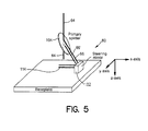
- FIG. 5 shows schematically the orientation of the primary splitter mirror 104 .
- the reflected light 66 , 66 ′ is steered into the optical plane of the wavemeter with the steering mirror 102 .
- the angle of incidence at the steering mirror 102 is 25°.
- the maximum fluence at the primary splitter mirror 104 is where the incident beam 66 at the chamber side primary surface 104 ′ and the beam 66 ′ reflected from the shutter side secondary surface 104 ′′ overlap ( FIG. 5 , being schematic and for illustration purposes, not showing any beam overlap).
- This maximum fluence can be estimated as follows:
- Total fluence 39.5 mJ/cm 2 .
- the fluence range is 26.3 to 52.6 mJ/cm 2 at the primary splitter mirror 104 .
- the maximum fluence level is given by:
- the fluence range at the steering mirror is 5.5 to 11.0 mJ/cm 2 .
- the overall optical layout within the SAM 46 optical portion 72 is shown.
- the light from the primary splitter mirror 104 is reflected into the optical plane of the wavemeter in beam 114 .
- the approximate fluences at the various optical elements leading up to the second stage diffuser 160 can be estimated, continuing with the assumptions made above.
- the range of fluences listed below are for 20 to 40 mJ/pulse energies, and assuming a 2.2 de-magnification ratio along the long axis of the beam 114 using a cylindrical telescope setup, as noted above:
- M1 adjustable mirror 146 4.1 to 8.3 mJ/cm 2
- Telescope front lens 204 5.8 to 11.7 mJ/cm 2
- Telescope rear lens 220 11.8 to 23.7 mJ/cm 2
- Diffractive diffuser 222 10.9 to 21.8 mJ/cm 2
- Focusing lens 224 7.6 to 15.3 mJ/cm 2
- Second stage diffuser 230 7 to 14 mJ/cm 2
- the fluence levels at the telescope rear lens 220 and the diffractive diffuser 222 can be considered to be considerably high, with a possibility of damage.
- a cylindrical telescope and/or utilized MgF 2 have, e.g., incorporated a cylindrical telescope and/or utilized MgF 2 .
- FIG. 6 there is shown the output signal levels from the PDA 182 in the SAM 46 for differing levels of fluence (20 mJ/pulse, 30 mJ/pulse and 40 mJ/pulse) and their intersection with the 1.5V signal output line.
- the incidence angles are respectively 65.9°, 70.8° and 73.2°. This is assuming a, e.g., 10 degree or so cone angle diffuser 230 .
- Making the diffractive diffuser from CaF 2 instead of fused silica is one choice.
- Another choice could be to, e.g., decrease the magnification of the combination of the front telescope lens 204 and the telescope rear lens 220 , to increase the size of the beam 114 incident on the diffractive diffuser 222 , thereby reducing the fluence per c 2 .
- a combination of the two, or even the selection of other possible fused silica materials along with de-magnification of the beam may be utilized.
- the front telescope lens 220 may be large enough to have acceptable fluence even with fused silica material.
- Comparable fluence levels incident on a ground glass diffuser may be ignored because compaction type damage to the element would not be expected to dramatically alter or affect its diffusing properties.
- the second stage diffuser 230 may be formed of a flat piece of glass with a grounded surface to induce diffusion which can then, e.g., be etched by bathing the surface, e.g., in a bath of ammonium bi-fluoride (“ABF”), which, among other things, enhances the diffusion uniformity.
- ABSF ammonium bi-fluoride
- the embodiment could also include other variations, e.g., the front telescope lens and the focusing lens made of ArF grade or better (from a compaction standpoint) fused silica.
- the front telescope lens and the focusing lens made of ArF grade or better (from a compaction standpoint) fused silica.
- Redesigning the illumination scheme to reduce the fluence levels at the diffractive diffuser 222 e.g., primarily by changing, e.g., the de-magnification ratio of the telescope produces considerable potential benefit.
- applicants have chosen a telescope with cylindrical lenses, and therefore, the orientation of the lenses would be such that only the long axis of the beam 114 would get de-magnified.
- the fluence at the diffractive diffuser 222 would be lower than that with a telescope consisting of similar spherical lenses, because the fluence can be better spread across the rectangular shape of the diffuser 222 , with its long axis coinciding with the long axis of the beam 114 .
- Another possible embodiment could entail removing the telescope system 204 , 220 altogether.
- a drawback from having an extended source incident on the diffractive diffuser 222 could be that the beam 114 angles incident on the ground glass diffuser 230 get steeper.
- the ground glass diffuser 230 that scrambles the angular information in the beam is not perfect. As the angle gets steeper, its ability to uniformly scramble the angular information in the beam 114 degrades. As a result, the whole source beam 114 may not be uniformly sampled by the etalon, thereby leading to inaccuracies in the metrology.
- the implementation of the embodiment utilizing spherical lenses can be further optimized by expanding the beam along the short axis, e.g., by using a prism.
- a prism For example, allowing for a 3 ⁇ beam expansion could result in, e.g., a 9 mm ⁇ 9 mm beam incident on the telescope system 204 , 220 .
- the beam After passing through, e.g., a 1.8 ⁇ de-magnification telescope the beam could be reduced, e.g., to a 5 mm ⁇ 9mm beam, with further reduced fluence levels at the diffractive diffuser 222 .
- the beam 114 size at the diffractive diffuser 222 e.g., by expanding the beam along the short axis and reducing the beam size along its long axis with the use of cylindrical lens pairs for each of the horizontal and vertical axes.
- the beam size could be, e.g., 4.8 mm ⁇ 5.6 mm beam. This could make an ideal system.
- expansion along the short axis could also increase the separation between the two Fresnel reflection images 66 , 66 ′ when incident on the aperture of the diffractive diffuser 222 .
- optics related improvements in the embodiments of the present invention relating to improving the efficiency and efficacy of beam homogenization include improving the low quantum efficiency of the PDA 182 used for fringe detection. Improving the detector efficiency could reduce the need to use relatively high fluences in the whole train of optics in the SAM 46 , and also in the LAM 28 , particularly beneficial in retaining fused silica optical components. However, if constrained to the same PDA 182 , the above-mentioned optical improvements could be necessary.
- a diffractive diffuser 222 made from calcium fluoride; use spherical lenses with the de-magnification ratio changed to 2.0; use cylindrical lenses with de-magnification ratio 2.0, remove the telescope; or use two cylindrical lenses and one spherical lens with 1.87 de-magnification along the long axis and 1.87 magnification along the short axis.
- Various combinations of materials and embodiments between CaF 2 and SF could also be availed by the choice of the particular solution.
- FIGS. 9 a and b , and 10 a and b are cross section of the mirror mount 260 , along the lines 10 b — 10 b in FIG. 10 a (except that the embodiment in FIG. 10 a has the mirror 264 removed), there is shown a perspective view of the front and the back of an adjustable mirror mounting 260 and mirror, e.g., mirror M 2 156 and the cross sectional view.
- the mirror 156 has an adjustable mirror mounting frame 260 , which may comprise an upper foot 270 extending laterally from a generally vertical mirror mounting portion 261 , along with a lower foot 272 , forming a base for the vertical portion 261 .
- FIG. 10 b being a cross section of the mirror mount 260 , along the lines 10 b — 10 b in FIG. 10 a (except that the embodiment in FIG. 10 a has the mirror 264 removed)
- the mirror 156 has an adjustable mirror mounting frame 260 , which may comprise an upper foot 270 extending laterally from a
- the vertical portion 261 and its upper foot 270 are attached to the lower foot 272 by means of a thin relatively narrow flexure 300 , so that the upper foot 270 and vertical mirror mounting portion 261 can bend with respect to the lower foot 272 , for alignment of the mirror 264 mounted on the mount 260 in the vertical plane of the incident beam (not shown), i.e., pivoting about the horizontal axis of the flexure 300 .
- the front face 263 of the vertical portion 262 is machined to have the surface 263 biased by about 2°-3° in order for there to be a constant spring force in the flexure 300 for purposes of maintaining a constant spring force during tilt adjustment.
- the mirror optic 264 is mounted in a recess in the rear side of the vertical portion 261 and is indexed to the working surface and clamped in place by a circular spring clip 310 , shown in greater detail in FIG. 10 c , which is in turn held in place by a plurality of spring clip mounting screws 312 .
- the indexing may be performed by utilizing, e.g., a plurality of spherical tooling balls 314 , one of which is shown in FIG. 10 b , which may be placed in machined openings in the vertical portion of the mount, e.g., 261 in FIG. 10 b and are aligned to engage the mirror or other optic being mounted, e.g., mirror 264 in FIG.
- FIG. 9 a uses a plurality of finger spring clips 320 .
- the mount 260 can be mounted on a dowel pin (not shown) extending into a dowel pin opening 304 in the bottom foot 272 , and pivoted to align the mirror 264 in the horizontal plane of the incident beam (not shown).
- the dowel pin opening 304 and the dowel pin it receives (not shown), which is mounted on the plate 122 are indexed to the required position of the optical plane of the optic, e.g., mirror 264 . That is, when the dowel pin (not shown) is inserted into the dowel pin opening 304 the mirror indexed in the mounting 260 is in precisely the plane it should be, e.g., when also aligned if pointing direction, if adjustable in that axis.
- the dowel pin and its receiving opening 304 therefore serve as a key to aligning the optical plane of the optic, e.g., mirror 264 , and also for horizontal pivoting, if required.
- a rotate adjustment locking screw 290 extending through a rotate adjustment locking screw opening 294 in the upper foot 270 and a similar opening 292 in the lower foot 272 , and into an arced slot (not shown) in the plate 122 of the SAM 46 , and held in place by a cap screw (not shown) fixes the horizontal alignment of the mount 260 .
- a vertical (tilt) adjustment screw 272 extending through a threaded opening 280 in the upper foot 270 and having a ball tip engaging the lower foot 272 can be utilized to set the tilt of the vertical portion 261 and this position may then be fixed by a tilt adjustment locking screw 266 extending through a tilt adjustment locking screw opening 268 in the upper foot 270 and into a threaded opening 274 in the lower foot.
- FIG. 10 a shows a similar mount 260 from which a mirror in the form of a circular mirror has been removed and on which is mounted a circular spring clip 310 , shown in more detail in FIG. 10 c .
- the circular spring clip 310 can have a ring portion 320 including a plurality of mounting screw extensions 322 in which are formed mounting screw holes 324 .
- the circular spring clip 310 also has a plurality of spring clip 330 attached to the ring by spring clip connections 332 and extending through spring clip arms 334 to a terminal extension at which may be placed a spring clip engagement protrusion 340 in the shape of hemisphere to facilitate engagement of, e.g., an optical element without damage to the optical element.
- FIG. 11 The embodiment shown in FIG. 11 is a secondary beam splitter mirror mount 350 , which is similar to those in FIGS. 9 and 10 without the upper and lower feet and flexure, i.e., a fixed and non adjustable mirror mount, e.g., for secondary beam splitter 140 .
- Shown in FIGS. 12 a-b is a mounting frame, e.g., mounting frame 152 for mounting the combination optical elements shown, e.g., in FIG. 7 .
- FIG. 12 a shows the combination optic mounting frame 360 comprising a telescope rear lens 220 held in place by a retaining clip 363 mounted to the combination optic mounting 360 by a pair of mounting screws 364 .
- FIG. 12 a shows the combination optic mounting frame 360 comprising a telescope rear lens 220 held in place by a retaining clip 363 mounted to the combination optic mounting 360 by a pair of mounting screws 364 .
- FIG. 12 b shows the back end of the mount 360 with the spherical focusing lens 224 held in place in a recess in the mount 360 by a plurality of finger spring clips that are attached to the mount by a plurality of mounting screws 372 .
- FIG. 12 b shows the mount with the focus lens 224 removed to show the first stage diffraction diffuser 222 held in place within the recess by a retaining clip attached to the mounting 360 by a pair of retaining clip mounting screws 382 .
- FIGS. 13 a and b show a slit assembly, e.g., for mounting the second stage diffuser, i.e., 160 as shown in FIG. 4 .
- the slit assembly mounting frame 390 may comprise a slit assembly 392 adjustably positioned on the mounting frame 390 by way of a pair of slots 400 and a respective pair of adjustment screws 404 on a front vertical portion 401 of the slit assembly 392 , as well as a side slot 402 extending vertically in a side portion 403 of the slit assembly, along with a side adjustment screw 406 .
- the front side of the slit assembly 390 faces the etalon as shown in FIG. 4 .
- the slit assembly 390 also includes in the front vertical portion the slit 394 attached to the slit assembly 392 by a pair of mounting screws 396 .
- FIG. 13 a shows the slit assembly 392 in the down position acting as an aperture for the second stage diffuser 230 , between the diffuser 230 and the etalon 162 .
- FIG. 13 b shows the slit assembly 392 in the retracted position for alignment between the diffuser 230 and the etalon 162 .
- FIG. 13 c shows the vertical positioning screw 412 threaded through a vertical positioning flange 418 on the mounting 390 and the second stage diffuser 230 held in place by a plurality of finge spring clips, with the slit assembly 392 in the down position.
- FIG. 13 d shows the slit assembly 392 in the retracted position.
- the slit opening 394 may also be adjusted side to side by horizontal adjustment screw 406 , with the slot 414 in the top of the assembly 392 accommodating side to side motion of screw 412 .
- the adjustment screws 406 and 412 have a very fine pitch, e.g., M 4 ⁇ 0.50, enabling very fine positioning of the slit assembly 392 to optically align the slit.
- These screws 406 , 412 may have hex-nut or the like tops to facilitate rotation with, e.g., an adjustment wrench.
- the angle of incidence for both the MO 22 output laser beam 62 and the PA 50 output laser beam 64 has been selected to be at least 70° in order to adequately protect the primary beam splitter mirror 104 from damage through exceeding the damage threshold of fluence for, e.g., MgF 2 and allowing sufficient room for each beam 62 , 64 to pass through the mirror 104 without the area of incidence of the beams 62 and 64 intersecting (though the fresnel reflections of both the passed and reflected portions of the PA beam may and most likely do overlap) and to provide an minimum of displacement of the path of the PA beam 64 .
- the 70° AOI of an embodiment of the present invention enables the secondary beam splitter to avoid exceeding its threshold of damage due, e.g., to high UV fluence level through the optic, even with exposure to the overlapped fresnel reflections in beam 114 .
- Differing materials used for the mirror 104 may also result in reducing the AOI at the primary beam splitter mirror 104 to somewhat less than 70°, but the AOI of the primary beam splitter will still be significantly larger than for prior lasers that neither have the overall output power requirements of lasers according to an embodiment of the present invention nor an output 62 of an MO laser chamber 22 sharing the available surface of the primary beam splitter mirror 104 .
- the etalon 162 slit function along with the focal length of the focusing lens 224 were selected to deliver to the photodiode array of the PDA 182 essentially only the innermost rings of the interference pattern created by the etalon, which also can be created by other optical interferometers, e.g., gratings, also having a slit function, so that the PDA can be assured over the range of the BW measurement and wavelength tuning of the laser to have at least one of the two interference rings with which to determine the pixel positions of the respective fringes in order to enable a BW calculation.
- the bandwidth calculation has been simplified to facilitate processing in the wavemeter microprocessor.
- the primary beam splitter 104 passes the vast majority of the output laser beam 64 from the PA 50 , i.e., approximately 95%, the exact amount of which may vary somewhat based upon such things as power requirements and fluence limits in the SAM, and reflects the remainder, a first small portion 114 , of the beam 64 to the SAM wavemeter.
- the beam splitter 140 in the wavemeter in the SAM 46 reflects the vast majority, e.g., approximately 95% of the first small portion 114 of the beam 64 to the PDM 144 .
- the present embodiment contemplates a detector employing an array of photodiodes.
- photosensitive elements e.g., photosensitive integrated circuits, e.g., CMOS or CCD devices could be used and when the term effectively illuminating each photodiode in a photodiode array is used it contemplates the effective illumination of other such forms of photo-sensitive elements.
- photodiodes over their entire vertical extent, i.e., 0.5 mm, but more efficient photodiodes or improvements in, e.g., the signal to noise ratio of their outputs could enable effective illumination (meaning an illumination which produces an acceptably accurate electrical output signal from the photosensitive element, e.g., the photodiode, that will enable measurement of the amplitude of the intensity of the light at the particular photo-sensitive element).
- effective illumination meaning an illumination which produces an acceptably accurate electrical output signal from the photosensitive element, e.g., the photodiode, that will enable measurement of the amplitude of the intensity of the light at the particular photo-sensitive element.
Abstract
Description
| Term/Acronym | Definition |
| ABF | Ammonium BiFluoride |
| ADC | Analog to digital converter |
| Amp | Amperes of current |
| AOI | Angle of Incidence |
| ArF | Argon Fluoride |
| AR | Anti-Reflection (a coating to reduce Fresnel reflection |
| from an optical surface) | |
| AWR | Absolute Wavelength Reference |
| BARO | Barometric station for alignment, calibration and test of |
| modules | |
| Blur | Compensation factor used to compensate for “bandwidth |
| saw-tooth” effect | |
| BW | Bandwidth |
| CaF2 | Calcium Fluoride |
| DD | Diffractive Diffuser |
| DFM | Design for Manufacturing |
| EWCM | Enhanced Wavelength Control Module |
| F2 | Fluorine |
| FCP | Fire Control Processor |
| FD | Focal distance |
| fm | femtometer |
| FRU | Field Replacement Units |
| FS | Fused Silica |
| FSR | Free Spectral Range |
| FWHM | Full Width at Half Maximum. A common metric for laser |
| bandwidth. | |
| GGD | Ground Glass Diffuser |
| KrF | Krypton Fluoride |
| LAM | Line center Analysis Module |
| LNM/LNP | Line Narrowing Module/Line Narrowing Package |
| MgF2 | Magnesium Fluoride |
| MOPA | Master Oscillator Power Amplifier |
| NIST | National Institute of Standards and Technology |
| PDA | Photodiode Array |
| PDM | Photodetector Module |
| pm | picometer |
| SAM | Spectral Analysis Module |
| WEB | Wavefront Engineering Box |
Δx=+0.0 mm
Δy=+1.33 mm
where it was assumed that the refractive index of N2 at 1 atm=1.0003.
Δx=+0.0 mm
Δy=+1.29 mm
which is not very different from the displacement with CaF2.
d=2*t*(tan θi)*(cos θi)
for θi=70° and using the material properties listed above,
| for CaF2, d | = 1.1 mm | |||
| for MgF2, d | = 1.2 mm | |||
| I11 | = I0y [{P70 Cos2(0)} + {S70 Sin2(0)}] | ||
| = I0y P70 | |||
I 12=(I 0y −I 11)P 70−(I 0y −I 11)(P 70)2
| IR | = I11 + I12 | |||
| for CaF2, | = 0.08133 I0y | |||
| for MgF2, | = 0.08632 I0y | |||
I 21 =S 45(I 11 +I 12)
I 22 =S 45(I 11 +I 12 −I 21)−(S 45)2(I 11 +I 12 −I 21)
| IR | = I21 + I22 | |||
| for CaF2, | = 0.0137 I0y | |||
| for MgF2, | = 0.01454 I0y | |||
| for CaF2, | = 0.00756 I0x | |||
| for MgF2, | = 0.00702 I0x | |||
| MO beam | ||||
| horizontal profile | 2.0 | mm | ||
| vertical profile | 7.5 | mm | ||
| PA beam | ||||
| horizontal profile | 5.0 | mm | ||
| vertical profile | 11.0 | mm | ||
| Center-to-center separation | 3.72 | mm | ||
| Tilt between MO and PA beams | 6.7 | mrad | ||
| Incident beam fluence | = Cos(70)*30.0/(0.9*0.3) | ||
| = 38 mJ/cm2 | |||
| Reflected beam fluence | = Cos(70)*(0.0389)*30.0/(0.9*0.3) | ||
| = 1.48 mJ/cm2 | |||
| Total fluence | = 39.5 mJ/cm2. | ||
For a range of 20 to 40 mJ/pulse, the fluence range is 26.3 to 52.6 mJ/cm2 at the
| Fluence from front face reflection | = Cos(25)*(0.0424)*30.0/(0.9*0.3) |
| = 4.27 mJ/cm2 | |
| Fluence from rear face reflection | = Cos(25)*(0.0389)*30.0/(0.9*0.3) |
| = 3.92 mJ/cm2 | |
| Total fluence | = 8.2 mJ/cm2. |
For a range of 20 to 40 mJ/pulse, the fluence range at the steering mirror (a dielectric coated optic) is 5.5 to 11.0 mJ/cm2.
| M1 adjustable mirror 146: | 4.1 to 8.3 mJ/cm2 | |||
| Telescope front lens 204: | 5.8 to 11.7 mJ/cm2 | |||
| Telescope rear lens 220: | 11.8 to 23.7 mJ/cm2 | |||
| Diffractive diffuser 222: | 10.9 to 21.8 mJ/cm2 | |||
| Focusing lens 224: | 7.6 to 15.3 mJ/cm2 | |||
| Second stage diffuser 230: | 7 to 14 mJ/cm2 | |||
Claims (35)
Priority Applications (9)
| Application Number | Priority Date | Filing Date | Title |
|---|---|---|---|
| US10/676,224 US6873418B1 (en) | 2003-09-30 | 2003-09-30 | Optical mountings for gas discharge MOPA laser spectral analysis module |
| KR1020067006227A KR101045226B1 (en) | 2003-09-30 | 2004-09-15 | Gas discharge mopa laser spectral analysis module |
| EP04784260.4A EP1668313B1 (en) | 2003-09-30 | 2004-09-15 | Gas discharge mopa laser spectral analysis module |
| EP04784259.6A EP1668312B1 (en) | 2003-09-30 | 2004-09-15 | Gas discharge mopa laser spectral analysis module |
| PCT/US2004/030340 WO2005033626A1 (en) | 2003-09-30 | 2004-09-15 | Gas discharge mopa laser spectral analysis module |
| JP2006533929A JP4773968B2 (en) | 2003-09-30 | 2004-09-15 | Spectral analysis module of gas discharge MOPA laser |
| JP2006533928A JP4787760B2 (en) | 2003-09-30 | 2004-09-15 | Spectral analysis module of gas discharge MOPA laser |
| PCT/US2004/030339 WO2005033625A1 (en) | 2003-09-30 | 2004-09-15 | Gas discharge mopa laser spectral analysis module |
| KR1020067006225A KR101186491B1 (en) | 2003-09-30 | 2004-09-15 | Gas discharge mopa laser spectral analysis module |
Applications Claiming Priority (1)
| Application Number | Priority Date | Filing Date | Title |
|---|---|---|---|
| US10/676,224 US6873418B1 (en) | 2003-09-30 | 2003-09-30 | Optical mountings for gas discharge MOPA laser spectral analysis module |
Publications (2)
| Publication Number | Publication Date |
|---|---|
| US6873418B1 true US6873418B1 (en) | 2005-03-29 |
| US20050068542A1 US20050068542A1 (en) | 2005-03-31 |
Family
ID=34314023
Family Applications (1)
| Application Number | Title | Priority Date | Filing Date |
|---|---|---|---|
| US10/676,224 Expired - Lifetime US6873418B1 (en) | 2003-09-30 | 2003-09-30 | Optical mountings for gas discharge MOPA laser spectral analysis module |
Country Status (1)
| Country | Link |
|---|---|
| US (1) | US6873418B1 (en) |
Cited By (5)
| Publication number | Priority date | Publication date | Assignee | Title |
|---|---|---|---|---|
| US20040240506A1 (en) * | 2000-11-17 | 2004-12-02 | Sandstrom Richard L. | DUV light source optical element improvements |
| US7471455B2 (en) | 2005-10-28 | 2008-12-30 | Cymer, Inc. | Systems and methods for generating laser light shaped as a line beam |
| US20110032609A1 (en) * | 2009-08-10 | 2011-02-10 | Chroma Technology Corporation | Microscope cube |
| US20110102893A1 (en) * | 2009-10-31 | 2011-05-05 | Gregory Solyar | Adjustable optical mount |
| CN102519355A (en) * | 2011-11-25 | 2012-06-27 | 中国科学院光电技术研究所 | One-dimensional micro-translation mechanism |
Families Citing this family (2)
| Publication number | Priority date | Publication date | Assignee | Title |
|---|---|---|---|---|
| US7088750B2 (en) * | 2003-12-05 | 2006-08-08 | Quartan Inc. | Adjustable laser module |
| DE102014109681B4 (en) * | 2014-07-10 | 2021-02-25 | Rofin-Baasel Lasertech Gmbh & Co. Kg | Convolution optics for a laser pulse compressor and laser pulse arrangement with a convolution optics |
Citations (49)
| Publication number | Priority date | Publication date | Assignee | Title |
|---|---|---|---|---|
| US4223279A (en) | 1977-07-18 | 1980-09-16 | Mathematical Sciences Northwest, Inc. | Pulsed electric discharge laser utilizing water dielectric blumlein transmission line |
| US4455658A (en) | 1982-04-20 | 1984-06-19 | Sutter Jr Leroy V | Coupling circuit for use with a transversely excited gas laser |
| US4959840A (en) | 1988-01-15 | 1990-09-25 | Cymer Laser Technologies | Compact excimer laser including an electrode mounted in insulating relationship to wall of the laser |
| US5023884A (en) | 1988-01-15 | 1991-06-11 | Cymer Laser Technologies | Compact excimer laser |
| US5025445A (en) | 1989-11-22 | 1991-06-18 | Cymer Laser Technologies | System for, and method of, regulating the wavelength of a light beam |
| US5025446A (en) | 1988-04-01 | 1991-06-18 | Laserscope | Intra-cavity beam relay for optical harmonic generation |
| US5189678A (en) | 1986-09-29 | 1993-02-23 | The United States Of America As Represented By The United States Department Of Energy | Coupling apparatus for a metal vapor laser |
| US5313481A (en) | 1993-09-29 | 1994-05-17 | The United States Of America As Represented By The United States Department Of Energy | Copper laser modulator driving assembly including a magnetic compression laser |
| US5315611A (en) | 1986-09-25 | 1994-05-24 | The United States Of America As Represented By The United States Department Of Energy | High average power magnetic modulator for metal vapor lasers |
| US5359620A (en) | 1992-11-12 | 1994-10-25 | Cymer Laser Technologies | Apparatus for, and method of, maintaining a clean window in a laser |
| US5448580A (en) | 1994-07-05 | 1995-09-05 | The United States Of America As Represented By The United States Department Of Energy | Air and water cooled modulator |
| US5471965A (en) | 1990-12-24 | 1995-12-05 | Kapich; Davorin D. | Very high speed radial inflow hydraulic turbine |
| US5543916A (en) * | 1993-10-04 | 1996-08-06 | Science Solutions, Inc. | Interferometer with alignment assembly and with processor for linearizing fringes for determining the wavelength of laser light |
| US5852621A (en) | 1997-07-21 | 1998-12-22 | Cymer, Inc. | Pulse laser with pulse energy trimmer |
| US5863017A (en) | 1996-01-05 | 1999-01-26 | Cymer, Inc. | Stabilized laser platform and module interface |
| US5953360A (en) | 1997-10-24 | 1999-09-14 | Synrad, Inc. | All metal electrode sealed gas laser |
| US5978394A (en) * | 1998-03-11 | 1999-11-02 | Cymer, Inc. | Wavelength system for an excimer laser |
| US6005879A (en) | 1997-04-23 | 1999-12-21 | Cymer, Inc. | Pulse energy control for excimer laser |
| US6016325A (en) | 1998-04-27 | 2000-01-18 | Cymer, Inc. | Magnetic modulator voltage and temperature timing compensation circuit |
| US6018537A (en) | 1997-07-18 | 2000-01-25 | Cymer, Inc. | Reliable, modular, production quality narrow-band high rep rate F2 laser |
| US6028880A (en) | 1998-01-30 | 2000-02-22 | Cymer, Inc. | Automatic fluorine control system |
| US6067311A (en) | 1998-09-04 | 2000-05-23 | Cymer, Inc. | Excimer laser with pulse multiplier |
| US6094448A (en) | 1997-07-01 | 2000-07-25 | Cymer, Inc. | Grating assembly with bi-directional bandwidth control |
| US6104735A (en) | 1999-04-13 | 2000-08-15 | Cymer, Inc. | Gas discharge laser with magnetic bearings and magnetic reluctance centering for fan drive assembly |
| US6128323A (en) | 1997-04-23 | 2000-10-03 | Cymer, Inc. | Reliable modular production quality narrow-band high REP rate excimer laser |
| US6151349A (en) | 1998-03-04 | 2000-11-21 | Cymer, Inc. | Automatic fluorine control system |
| US6164116A (en) | 1999-05-06 | 2000-12-26 | Cymer, Inc. | Gas module valve automated test fixture |
| US6192064B1 (en) | 1997-07-01 | 2001-02-20 | Cymer, Inc. | Narrow band laser with fine wavelength control |
| US6208675B1 (en) | 1998-08-27 | 2001-03-27 | Cymer, Inc. | Blower assembly for a pulsed laser system incorporating ceramic bearings |
| US6208674B1 (en) | 1998-09-18 | 2001-03-27 | Cymer, Inc. | Laser chamber with fully integrated electrode feedthrough main insulator |
| US6219368B1 (en) | 1999-02-12 | 2001-04-17 | Lambda Physik Gmbh | Beam delivery system for molecular fluorine (F2) laser |
| US6240117B1 (en) | 1998-01-30 | 2001-05-29 | Cymer, Inc. | Fluorine control system with fluorine monitor |
| US6317448B1 (en) | 1999-09-23 | 2001-11-13 | Cymer, Inc. | Bandwidth estimating technique for narrow band laser |
| US6330261B1 (en) | 1997-07-18 | 2001-12-11 | Cymer, Inc. | Reliable, modular, production quality narrow-band high rep rate ArF excimer laser |
| US20020006149A1 (en) | 2000-02-09 | 2002-01-17 | Spangler Ronald L. | Laser wavelength control unit with piezoelectric driver |
| US20020048288A1 (en) | 1997-07-22 | 2002-04-25 | Armen Kroyan | Laser spectral engineering for lithographic process |
| US6414979B2 (en) | 2000-06-09 | 2002-07-02 | Cymer, Inc. | Gas discharge laser with blade-dielectric electrode |
| US20020101589A1 (en) | 2001-01-29 | 2002-08-01 | Sandstrom Richard L. | High resolution etalon-grating spectrometer |
| US20020154671A1 (en) | 1999-05-10 | 2002-10-24 | Knowles David S. | Line selected F2 two chamber laser system |
| US20020154668A1 (en) | 1999-12-10 | 2002-10-24 | Knowles David S. | Very narrow band, two chamber, high rep rate gas discharge laser system |
| US6477193B2 (en) | 1998-07-18 | 2002-11-05 | Cymer, Inc. | Extreme repetition rate gas discharge laser with improved blower motor |
| US20030012234A1 (en) | 2000-06-19 | 2003-01-16 | Watson Tom A. | Six to ten KHz, or greater gas discharge laser system |
| US20030018072A1 (en) | 1998-11-19 | 2003-01-23 | Joshi Rajendra Kumar | Utilization of dialkylfumarates |
| US6539046B2 (en) * | 1998-10-02 | 2003-03-25 | Cymer, Inc. | Wavemeter for gas discharge laser |
| US20030099269A1 (en) | 2001-05-03 | 2003-05-29 | Ershov Alexander I. | Timing control for two-chamber gas discharge laser system |
| US20030138019A1 (en) | 2002-01-23 | 2003-07-24 | Rylov German E. | Two chamber F2 laser system with F2 pressure based line selection |
| US6690704B2 (en) | 2001-04-09 | 2004-02-10 | Cymer, Inc. | Control system for a two chamber gas discharge laser |
| US6693939B2 (en) | 2001-01-29 | 2004-02-17 | Cymer, Inc. | Laser lithography light source with beam delivery |
| US6750972B2 (en) * | 2000-11-17 | 2004-06-15 | Cymer, Inc. | Gas discharge ultraviolet wavemeter with enhanced illumination |
-
2003
- 2003-09-30 US US10/676,224 patent/US6873418B1/en not_active Expired - Lifetime
Patent Citations (50)
| Publication number | Priority date | Publication date | Assignee | Title |
|---|---|---|---|---|
| US4223279A (en) | 1977-07-18 | 1980-09-16 | Mathematical Sciences Northwest, Inc. | Pulsed electric discharge laser utilizing water dielectric blumlein transmission line |
| US4455658A (en) | 1982-04-20 | 1984-06-19 | Sutter Jr Leroy V | Coupling circuit for use with a transversely excited gas laser |
| US5315611A (en) | 1986-09-25 | 1994-05-24 | The United States Of America As Represented By The United States Department Of Energy | High average power magnetic modulator for metal vapor lasers |
| US5189678A (en) | 1986-09-29 | 1993-02-23 | The United States Of America As Represented By The United States Department Of Energy | Coupling apparatus for a metal vapor laser |
| US4959840A (en) | 1988-01-15 | 1990-09-25 | Cymer Laser Technologies | Compact excimer laser including an electrode mounted in insulating relationship to wall of the laser |
| US5023884A (en) | 1988-01-15 | 1991-06-11 | Cymer Laser Technologies | Compact excimer laser |
| US5025446A (en) | 1988-04-01 | 1991-06-18 | Laserscope | Intra-cavity beam relay for optical harmonic generation |
| US5025445A (en) | 1989-11-22 | 1991-06-18 | Cymer Laser Technologies | System for, and method of, regulating the wavelength of a light beam |
| US5471965A (en) | 1990-12-24 | 1995-12-05 | Kapich; Davorin D. | Very high speed radial inflow hydraulic turbine |
| US5359620A (en) | 1992-11-12 | 1994-10-25 | Cymer Laser Technologies | Apparatus for, and method of, maintaining a clean window in a laser |
| US5313481A (en) | 1993-09-29 | 1994-05-17 | The United States Of America As Represented By The United States Department Of Energy | Copper laser modulator driving assembly including a magnetic compression laser |
| US5543916A (en) * | 1993-10-04 | 1996-08-06 | Science Solutions, Inc. | Interferometer with alignment assembly and with processor for linearizing fringes for determining the wavelength of laser light |
| US5448580A (en) | 1994-07-05 | 1995-09-05 | The United States Of America As Represented By The United States Department Of Energy | Air and water cooled modulator |
| US5863017A (en) | 1996-01-05 | 1999-01-26 | Cymer, Inc. | Stabilized laser platform and module interface |
| US6005879A (en) | 1997-04-23 | 1999-12-21 | Cymer, Inc. | Pulse energy control for excimer laser |
| US6128323A (en) | 1997-04-23 | 2000-10-03 | Cymer, Inc. | Reliable modular production quality narrow-band high REP rate excimer laser |
| US6094448A (en) | 1997-07-01 | 2000-07-25 | Cymer, Inc. | Grating assembly with bi-directional bandwidth control |
| US6192064B1 (en) | 1997-07-01 | 2001-02-20 | Cymer, Inc. | Narrow band laser with fine wavelength control |
| US6330261B1 (en) | 1997-07-18 | 2001-12-11 | Cymer, Inc. | Reliable, modular, production quality narrow-band high rep rate ArF excimer laser |
| US6018537A (en) | 1997-07-18 | 2000-01-25 | Cymer, Inc. | Reliable, modular, production quality narrow-band high rep rate F2 laser |
| US5852621A (en) | 1997-07-21 | 1998-12-22 | Cymer, Inc. | Pulse laser with pulse energy trimmer |
| US20020048288A1 (en) | 1997-07-22 | 2002-04-25 | Armen Kroyan | Laser spectral engineering for lithographic process |
| US5953360A (en) | 1997-10-24 | 1999-09-14 | Synrad, Inc. | All metal electrode sealed gas laser |
| US6240117B1 (en) | 1998-01-30 | 2001-05-29 | Cymer, Inc. | Fluorine control system with fluorine monitor |
| US6028880A (en) | 1998-01-30 | 2000-02-22 | Cymer, Inc. | Automatic fluorine control system |
| US6151349A (en) | 1998-03-04 | 2000-11-21 | Cymer, Inc. | Automatic fluorine control system |
| US5978394A (en) * | 1998-03-11 | 1999-11-02 | Cymer, Inc. | Wavelength system for an excimer laser |
| US6016325A (en) | 1998-04-27 | 2000-01-18 | Cymer, Inc. | Magnetic modulator voltage and temperature timing compensation circuit |
| US6477193B2 (en) | 1998-07-18 | 2002-11-05 | Cymer, Inc. | Extreme repetition rate gas discharge laser with improved blower motor |
| US6208675B1 (en) | 1998-08-27 | 2001-03-27 | Cymer, Inc. | Blower assembly for a pulsed laser system incorporating ceramic bearings |
| US6067311A (en) | 1998-09-04 | 2000-05-23 | Cymer, Inc. | Excimer laser with pulse multiplier |
| US6208674B1 (en) | 1998-09-18 | 2001-03-27 | Cymer, Inc. | Laser chamber with fully integrated electrode feedthrough main insulator |
| US6539046B2 (en) * | 1998-10-02 | 2003-03-25 | Cymer, Inc. | Wavemeter for gas discharge laser |
| US20030018072A1 (en) | 1998-11-19 | 2003-01-23 | Joshi Rajendra Kumar | Utilization of dialkylfumarates |
| US6219368B1 (en) | 1999-02-12 | 2001-04-17 | Lambda Physik Gmbh | Beam delivery system for molecular fluorine (F2) laser |
| US6104735A (en) | 1999-04-13 | 2000-08-15 | Cymer, Inc. | Gas discharge laser with magnetic bearings and magnetic reluctance centering for fan drive assembly |
| US6164116A (en) | 1999-05-06 | 2000-12-26 | Cymer, Inc. | Gas module valve automated test fixture |
| US20020154671A1 (en) | 1999-05-10 | 2002-10-24 | Knowles David S. | Line selected F2 two chamber laser system |
| US6317448B1 (en) | 1999-09-23 | 2001-11-13 | Cymer, Inc. | Bandwidth estimating technique for narrow band laser |
| US20020154668A1 (en) | 1999-12-10 | 2002-10-24 | Knowles David S. | Very narrow band, two chamber, high rep rate gas discharge laser system |
| US6625191B2 (en) | 1999-12-10 | 2003-09-23 | Cymer, Inc. | Very narrow band, two chamber, high rep rate gas discharge laser system |
| US20020006149A1 (en) | 2000-02-09 | 2002-01-17 | Spangler Ronald L. | Laser wavelength control unit with piezoelectric driver |
| US6414979B2 (en) | 2000-06-09 | 2002-07-02 | Cymer, Inc. | Gas discharge laser with blade-dielectric electrode |
| US20030012234A1 (en) | 2000-06-19 | 2003-01-16 | Watson Tom A. | Six to ten KHz, or greater gas discharge laser system |
| US6750972B2 (en) * | 2000-11-17 | 2004-06-15 | Cymer, Inc. | Gas discharge ultraviolet wavemeter with enhanced illumination |
| US20020101589A1 (en) | 2001-01-29 | 2002-08-01 | Sandstrom Richard L. | High resolution etalon-grating spectrometer |
| US6693939B2 (en) | 2001-01-29 | 2004-02-17 | Cymer, Inc. | Laser lithography light source with beam delivery |
| US6690704B2 (en) | 2001-04-09 | 2004-02-10 | Cymer, Inc. | Control system for a two chamber gas discharge laser |
| US20030099269A1 (en) | 2001-05-03 | 2003-05-29 | Ershov Alexander I. | Timing control for two-chamber gas discharge laser system |
| US20030138019A1 (en) | 2002-01-23 | 2003-07-24 | Rylov German E. | Two chamber F2 laser system with F2 pressure based line selection |
Cited By (9)
| Publication number | Priority date | Publication date | Assignee | Title |
|---|---|---|---|---|
| US20040240506A1 (en) * | 2000-11-17 | 2004-12-02 | Sandstrom Richard L. | DUV light source optical element improvements |
| US7346093B2 (en) * | 2000-11-17 | 2008-03-18 | Cymer, Inc. | DUV light source optical element improvements |
| US7471455B2 (en) | 2005-10-28 | 2008-12-30 | Cymer, Inc. | Systems and methods for generating laser light shaped as a line beam |
| US20110032609A1 (en) * | 2009-08-10 | 2011-02-10 | Chroma Technology Corporation | Microscope cube |
| US8488238B2 (en) * | 2009-08-10 | 2013-07-16 | Chroma Technology Corporation | Microscope cube |
| US20110102893A1 (en) * | 2009-10-31 | 2011-05-05 | Gregory Solyar | Adjustable optical mount |
| US8172412B2 (en) | 2009-10-31 | 2012-05-08 | Lenox Laser Corporation | Adjustable optical mount |
| CN102519355A (en) * | 2011-11-25 | 2012-06-27 | 中国科学院光电技术研究所 | One-dimensional micro-translation mechanism |
| CN102519355B (en) * | 2011-11-25 | 2014-07-09 | 中国科学院光电技术研究所 | One-dimensional micro-translation mechanism |
Also Published As
| Publication number | Publication date |
|---|---|
| US20050068542A1 (en) | 2005-03-31 |
Similar Documents
| Publication | Publication Date | Title |
|---|---|---|
| US7292343B2 (en) | Gas discharge MOPA laser spectral analysis module | |
| US6894785B2 (en) | Gas discharge MOPA laser spectral analysis module | |
| US5978394A (en) | Wavelength system for an excimer laser | |
| US7382815B2 (en) | Laser spectral engineering for lithographic process | |
| US6160831A (en) | Wavelength calibration tool for narrow band excimer lasers | |
| EP0992093B1 (en) | Wavelength system for an excimer laser | |
| US6317448B1 (en) | Bandwidth estimating technique for narrow band laser | |
| JP2005501399A (en) | Laser spectral engineering for lithographic processing | |
| JP2005530352A (en) | Gas discharge ultraviolet wavelength meter with improved illumination | |
| US10288484B2 (en) | Homogenization of light beam for spectral feature metrology | |
| US6873418B1 (en) | Optical mountings for gas discharge MOPA laser spectral analysis module | |
| EP1668313B1 (en) | Gas discharge mopa laser spectral analysis module | |
| US6542243B2 (en) | Resonator optics monitoring method | |
| US20040141182A1 (en) | Monitoring of spectral purity and advanced spectral characteristics of a narrow bandwidth excimer laser | |
| JP4773968B2 (en) | Spectral analysis module of gas discharge MOPA laser | |
| CN100538259C (en) | Gas discharge MOPA laser spectral analysis module |
Legal Events
| Date | Code | Title | Description |
|---|---|---|---|
| AS | Assignment |
Owner name: CYMER, INC., CALIFORNIA Free format text: ASSIGNMENT OF ASSIGNORS INTEREST;ASSIGNORS:HOWEY, JAMES K.;RAN, RAJASEKHAR M.;REEL/FRAME:014672/0283 Effective date: 20030929 |
|
| STCF | Information on status: patent grant |
Free format text: PATENTED CASE |
|
| CC | Certificate of correction | ||
| FPAY | Fee payment |
Year of fee payment: 4 |
|
| FPAY | Fee payment |
Year of fee payment: 8 |
|
| FEPP | Fee payment procedure |
Free format text: PAYOR NUMBER ASSIGNED (ORIGINAL EVENT CODE: ASPN); ENTITY STATUS OF PATENT OWNER: LARGE ENTITY |
|
| AS | Assignment |
Owner name: CYMER, LLC, CALIFORNIA Free format text: MERGER;ASSIGNOR:CYMER, INC.;REEL/FRAME:032397/0280 Effective date: 20130530 |
|
| FPAY | Fee payment |
Year of fee payment: 12 |