US6883060B1 - Microcomputer provided with flash memory and method of storing program into flash memory - Google Patents
Microcomputer provided with flash memory and method of storing program into flash memory Download PDFInfo
- Publication number
- US6883060B1 US6883060B1 US09/401,293 US40129399A US6883060B1 US 6883060 B1 US6883060 B1 US 6883060B1 US 40129399 A US40129399 A US 40129399A US 6883060 B1 US6883060 B1 US 6883060B1
- Authority
- US
- United States
- Prior art keywords
- rewriting
- flash memory
- area
- program
- flag
- Prior art date
- Legal status (The legal status is an assumption and is not a legal conclusion. Google has not performed a legal analysis and makes no representation as to the accuracy of the status listed.)
- Expired - Fee Related
Links
Images


Classifications
-
- G—PHYSICS
- G06—COMPUTING; CALCULATING OR COUNTING
- G06F—ELECTRIC DIGITAL DATA PROCESSING
- G06F11/00—Error detection; Error correction; Monitoring
- G06F11/30—Monitoring
- G06F11/34—Recording or statistical evaluation of computer activity, e.g. of down time, of input/output operation ; Recording or statistical evaluation of user activity, e.g. usability assessment
-
- G—PHYSICS
- G06—COMPUTING; CALCULATING OR COUNTING
- G06F—ELECTRIC DIGITAL DATA PROCESSING
- G06F8/00—Arrangements for software engineering
- G06F8/60—Software deployment
- G06F8/65—Updates
-
- G—PHYSICS
- G11—INFORMATION STORAGE
- G11C—STATIC STORES
- G11C16/00—Erasable programmable read-only memories
- G11C16/02—Erasable programmable read-only memories electrically programmable
- G11C16/06—Auxiliary circuits, e.g. for writing into memory
- G11C16/10—Programming or data input circuits
- G11C16/102—External programming circuits, e.g. EPROM programmers; In-circuit programming or reprogramming; EPROM emulators
Definitions
- This invention relates to a microcomputer provided with a flash memory and a method of storing a program into a flash memory, and more particularly to a microcomputer having a self-programming function of rewriting a program stored in a flash memory and a method of storing a program into a flash memory.
- a data processing apparatus which detects an interruption of rewriting processing of a flash memory to prevent a malfunction is conventionally known and disclosed in Japanese Patent Laid-Open No. 6865/1996.
- FIG. 1 is a block diagram showing a general configuration of the data processing apparatus disclosed in the document mentioned above.
- CPU 202 performs, upon initialization of such as changing of a program, rewriting processing of writing data block by block from ROM 203 into flash memory 204 through RAM 206 and writing a start code and an end code representative of a start/end of data in a corresponding relationship to the data into flash memory 204 .
- CPU 202 copies contents of flash memory 204 into RAM 206 each time power supply is made available. Upon such copying, CPU 202 detects a write failure of the data in flash memory 204 based on the start code and the end code.
- FIG. 2 shows a data structure of flash memory 204 .
- Flash memory 204 is divided into a plurality of blocks.
- a data train including data train 101 , start code 103 and end code 104 is written into each of the blocks.
- Start code 103 and end code 104 are predetermined arbitrary data and added to the start and the end of data train 101 .
- FIG. 3 is a flow chart illustrating processing of the conventional data processing apparatus when a normal program is started.
- step C 1 Data for one block are read out from flash memory 204 (step C 1 ), and the start code and the end code are compared with respective expected values (step C 2 ). Then, a result of the comparison in step C 2 is confirmed (step C 3 ). In such a case that rewriting of data of a block read formerly has been interrupted halfway, the end code or the start code and the end code have not been written as yet, and therefore, the start code and the end code do not coincide with the respective expected values. Thus, setting of flash memory 204 and RAM 206 is performed (step C 4 ), and error processing is performed (step C 5 ). Then, the normal program stored in RAM 206 is started for execution (step CB).
- step C 3 If it is confirmed in step C 3 that the start code and the end code coincide with the respective expected values, then the block is written into RAM 206 (step C 6 ). Then, it is confirmed whether the processing has been completed for all data or not (step C 7 ). If the processing for all data has been completed, then the normal program stored in RAM 206 is started for execution (step C 8 ). If it is confirmed in step C 7 that the processing for all data has not been completed, the control returns to step C 1 to repeat the operations of steps C 1 to C 6 until transfer of the data for the predetermined blocks to the RAM is completed.
- the first problem is that, because writing of a start code and an end code for detecting a write failure of the flash memory is performed only upon rewriting of the flash memory, a write failure cannot be detected if it occurs when the rewriting processing is interrupted in an initial stage.
- the start code and the end code may possibly remain without being erased even though some of the program codes have been erased already. In this case, a malfunction may occur.
- the second problem is that, because a start code and an end code are added as part of the write data of a data area when they are provided on the boundary between blocks, it is difficult to produce a program since the CPU directly executes a program existing in the flash memory.
- a computer system sometimes has a configuration such that a reset vector or an interrupt vector is fixed to a particular address. In a computer system of this type, if a reset vector or an interrupt vector is fixed to an address into which a start code or an encode should be stored, a program cannot be produced.
- a conventional data processing apparatus is configured to read a program into the RAM once and then execute the program, when it employs a computer having a built-in memory like a single chip microcomputer, a RAM for storing a program to be executed must be prepared additionally for the data processing apparatus, resulting in a higher cost for the data processing apparatus.
- the conventional data processing apparatus has a further problem that much time is required to start a normal processing program since the program is transferred from the flash memory to the RAM.
- the present invention has been made in view of the various problems of the prior art described above, and it is an object of the present invention to provide a microcomputer provided with a built-in flash memory and having a self-programming function and a method of storing a program into a flash memory by which a write failure which arises from an interruption of rewriting processing of the flash memory can be detected rapidly and with certainty.
- a microcomputer provided with a flash memory and having a self-programming function of rewriting a program stored in the flash memory, comprising a rewrite program area for storing a program for a rewriting processing procedure for the flash memory, and a controller for forming a plurality of flag areas locally in the flash memory when the rewriting program stored in external storage means or the rewrite program area is written into the flash memory, performing determination of completion of a plurality of stages of rewriting processing or determination of whether the plurality of stages are good or bad and recording results of the determination into the respective flag areas.
- the flash memory may include a plurality of blocks each of which is an erasable unit and includes a data area and a flag area, and the controller may map the data areas of the plurality of blocks to successive addresses.
- a microcomputer provided with a flash memory and having a self-programming function of rewriting a program stored in the flash memory, comprising a rewrite program area for storing a program for a rewriting processing procedure for the flash memory, rewriting means for forming a plurality of flag areas locally in the flash memory when the rewriting program stored in external storage means or the rewrite program area is written into the flash memory, and a controller for performing determination of completion of a plurality of stages of rewriting processing or determination of whether the plurality of stages are good or bad and recording results of the determination into the respective flag areas through the rewriting means.
- a microcomputer provided with a flash memory and having a self-programming function of rewriting a program stored in the flash memory, comprising a rewrite program area for storing a program for a rewriting processing procedure for the flash memory, rewriting means for forming a plurality of flag areas locally in the flash memory when the rewriting program stored in external storage means or the rewrite program area is written into the flash memory, a controller for performing determination of completion of a plurality of stages of rewriting processing or determination of whether the plurality of stages are good or bad and recording results of the determination into the respective flag areas through the rewriting means, and flag state notification means for comparing, when power supply is made available after the rewriting is completed, values read out from the flag areas with expected values for the flag areas stored in advance and notifying the controller of results of the comparison.
- the flash memory may include a plurality of blocks each of which is an erasable unit and includes a data area and a flag area, and the rewriting means may map the data areas of the plurality of blocks to successive addresses.
- part of the flash memory is used for flags into which a situation of procedure of rewriting processing of the flash memory should be recorded.
- the situation of procedure of rewriting can be grasped by confirming the contents of the flags. Consequently, a write failure which arises from an interruption of rewriting processing of the flash memory can be detected rapidly and with certainty.
- FIG. 1 is a block diagram showing a conventional data processing apparatus
- FIG. 2 is a diagrammatic view showing a data structure of a flash memory of a conventional data processing apparatus
- FIG. 3 is a flow chart illustrating processing of a conventional data processing apparatus when a normal program is starts
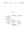
- FIG. 4 is a block diagram showing a configuration of an embodiment of the present invention.
- FIGS. 5 (A) and 5 (B) are diagrammatic views showing a configuration of flash area 4 shown in FIG. 4 , and wherein FIG. 5 (A) shows a physical configuration and FIG. 5 (B) shows a logical configuration;
- FIG. 6 is a flow chart illustrating operation of the embodiment when power supply is made available
- FIGS. 7 (A) and 7 (B) are diagrammatic views showing details of the configuration of flash area 4 , and wherein FIG. 7 (A) shows a physical configuration and FIG. 7 (B) shows a logical configuration;
- FIG. 8 is a diagrammatic view showing a configuration of flag area 2 ;
- FIG. 9 is a flow chart illustrating operation for rewriting processing of the flag area shown in FIG. 8 ;
- FIG. 10 is a block diagram showing a configuration of a second embodiment of the present invention.
- FIG. 4 is a block diagram showing a configuration of an embodiment of the present invention.
- the present embodiment includes microcomputer 1 , CPU (control means) 2 , rewriting program area 3 , flash area 4 , rewriting means 5 for rewriting flash area 4 , RAM 6 for storing temporary data in processing, and communication means 7 for interconnecting the components.
- FIGS. 5 (A) and 5 (B) are diagrammatic views showing a configuration of flash area 4 , and wherein FIG. 5 (A) shows a physical configuration and FIG. 5 (B) shows a logical configuration.
- Flash area 4 includes a plurality of blocks each of which forms an erasable unit and includes a flag area for storing a history of rewriting processing and a data area for storing a program, a data table and other necessary data.
- block 1 which includes data area 1 and flag area 1 is denoted by data 101
- block 2 which includes data area 2 and flag area 2 is denoted by 102 .
- the data areas are mapped at logical addresses in continuous space.
- FIG. 6 is a flow chart illustrating operation of the present embodiment when power supply is made available. Operation of the present embodiment will be described below with reference to FIG. 6 .
- Rewriting program area 3 stores a program for rewriting flash area 4 . Processing by the program stored in flash area 4 is illustrated on the right side of a broken line in FIG. 6 , and processing by the program stored in rewriting program area 3 is illustrated on the left side of the broken line.
- step A 1 initialization processing for setting the components to initial states is performed. After the initialization processing, it is checked whether a rewriting request for flash area 4 is present or not (step A 2 ). If a rewriting request for flash area 4 is present, then the rewriting operation is performed (step A 3 ), but if no rewriting request for flash area 4 is present, then it is determined whether the rewriting processing for flash area 4 has been performed regularly (step A 4 ).
- the determination of the regularity of the rewriting processing for the flash area in step A 4 depends upon determination of whether the flag areas shown in FIG. 5 (A) have expected values. If it is determined that the rewriting processing has not been performed regularly, then error processing is performed (step A 5 ), but if it is determined that the rewriting processing has been performed regularly, then normal processing by the program stored in flash area 4 is executed (step A 6 ).
- FIGS. 7 (A) and 7 (B) are diagrammatic views showing details of the configuration of flash area 4 , and wherein FIG. 7 (A) shows a physical configuration and FIG. 7 (B) shows a logical configuration.
- the configuration of flash area 4 shown in FIGS. 7 (A) and 7 (B) includes, in addition to the configuration of flash area 4 shown in FIGS. 5 (A) and 5 (B), rewriting program area 3 for explaining an example of allocation of addresses and RAM 6 for storing temporary data in processing.
- Rewriting program area 3 stores the program for rewriting flash area 4 .
- Flash area 4 stores a program for normal operation.
- the program stored in flash area 4 can be changed to augment functions of the system which employs the present embodiment or to amend a program to eliminate a defect of it.
- Rewriting of flash area 4 is performed by rewriting means 5 under the control of CPU 2 in accordance with the program stored in rewriting program area (ROM) 3 .
- the program in flash area 4 is rewritten into program codes received by communication means 7 .
- RAM 6 temporarily stores data during operation of a normal program or upon rewriting of rewriting program area 3 .
- FIG. 7 (A) While the example illustrated in FIG. 7 (A) includes RAM 6 , rewriting program area 3 and flash area 4 which includes 3 blocks each including a data area of 8 Kbytes and a flag area of 1 byte, in order to facilitate production of a program, the memory areas may be mapped in such a manner as illustrated in FIG. 7 (B) so that the data areas can be assured continuously in flash area 4 .
- FIG. 8 is a diagrammatic view showing a configuration of flag area 2 .
- a flash EEPROM or an EPROM has a common characteristic that a bit which has not been changed to a write value upon writing can be changed later by performing writing to the bit again.
- a flash EEPROM or an EPROM is configured so that a bit is changed to “0” by bit erasure but changed to “1” by bit writing, it is possible to write “1” to the 0th bit once and write “1” to the remaining bits later. However, a bit to which “1” is written once cannot be returned to “1” by later writing.
- FIG. 8 makes use of the fact just described to allocate the flags to 1 byte which is one write unit.
- a verify error flag a blank error flag, a rewriting end flag, a verify end flag, a write end flag, a black check end flag, an erasure end flag and a rewriting start flag are allocated, respectively.
- flags may be allocated in a size of a write unit such as 1 byte.
- the flags to be allocated must include at least the rewriting start flag and the rewriting end flag in order to achieve the principal object of the present invention.
- the flags to be allocated should be selected so as to keep a more detailed history so that, when writing is performed after an interruption of rewriting is detected, the rewriting can be performed efficiently by proceeding with the rewriting processing beginning with a process following the process at which the rewriting has been interrupted.
- FIG. 9 is a flow chart illustrating operation for rewriting processing of the flag area shown in FIG. 8 , and the rewriting processing will be described below with reference to FIG. 9 .
- the following description proceeds on the presumption that the value of each cell of the flash memory is changed to “0” by erasure and to “1” by writing.
- the flag area has a value “00111110” which is an expected value when rewriting is completed regularly, and in order to set the rewriting start flag which represents that rewriting processing is started, writing into the flag area is performed to change the value of the flag area to “00111111” (step B 1 ).
- the setting of the rewriting start flag makes the program stored at present in rewriting program area 3 different from an expected program. Therefore, even if the rewriting processing is interrupted in its initial stage, such interruption of the rewriting processing can be detected from the difference.
- step B 2 erasure of the rewriting area is performed. Thereupon, also the flag area is erased. Consequently, the flag area now has a value “00000000” without specifically designating the flag area for the change.
- step B 3 the erasure end flag which represents that erasure is completed is set (step B 3 ) to change the value of the flag area to “00000010”.
- a blank check of the data area is performed in order to confirm whether the erasure has been performed completely (step B 4 ), and then a result of the blank check is confirmed (step B 5 ). If the blank check reveals some incoincidence, the blank error flag is set (step B 6 ). Alternatively, however, the processing beginning with the erasure described above may be performed again.
- step B 7 the blank check end flag is set (step B 7 ) to change the value of the flag area to “00000110”, and then writing processing is performed continuously (step B 8 ).
- step B 9 the writing end flag is set (step B 9 ) to change the value of the flag area to “00001110”, and a verify operation for confirmation of whether the writing has been performed regularly is performed (step B 10 ).
- step B 11 a result of the verify processing is confirmed. If it is confirmed from the result of the verify processing that the writing has not been performed regularly, the verify error flag is set (step B 12 ). Alternatively, however, the writing operation may be performed again.
- step B 13 , B 14 the verify end flag and the rewriting end flag are set (steps B 13 , B 14 ), thereby ending the rewriting processing.
- a history representing that the step is completed is recorded into the flag area. Consequently, when a normal program is started, it can be detected whether rewriting processing is completed or not and in which stage the processing is interrupted by confirming the flag area of flash area 4 .
- FIG. 10 is a block diagram showing a configuration of a second embodiment of the present invention. The second embodiment of the present invention will be described below with reference to FIG. 10 .
- the present embodiment is different from the first embodiment in the configuration of rewriting means 5 which, in the first embodiment, merely performs a rewriting operation in order to reduce the burden to CPU 2 .
- the present embodiment is similar in the components to those of the first embodiment shown in FIG. 4 , and the like components thereof are denoted by like reference numerals and overlapping description of them is omitted here to avoid redundancy.
- Rewriting means 5 in the present embodiment includes rewriting control circuit 8 , data holding means 9 , rewrite state holding means 10 , and multiplexer (MPX) 11 .
- Rewriting control circuit 8 controls data holding means 9 , rewrite state holding means 10 and multiplexer 11 to effect control of designation of a rewriting area in flash area 4 and control of rewriting of flash area 4 such as writing and erasure.
- Rewriting control circuit 8 outputs address information of a block which is an object of rewriting and address information of a flag for the block.
- Data holding means 9 stores write data for the data area in flash area 4 , and outputs the write data to multiplexer 11 under the control of rewriting control circuit 8 .
- Rewrite state holding means 10 stores information regarding different processing stages of rewriting processing and information of a block which is an object of rewriting.
- Multiplexer 11 is controlled by rewriting control circuit 8 such that, upon writing into the data area, multiplexer 11 selects the output of data holding means 9 and outputs it to flash area 4 , but upon writing into the flag area, multiplexer 11 selects an output value of rewrite state holding means 10 and outputs it to flash area 4 .
- the output value from rewrite state holding means 10 to multiplexer 11 is a value which is written into the flag area when each process of rewriting processing is completed, and is updated by rewriting control circuit 8 each time the control advances to a next processing stage.
- rewriting of each flag area in the present embodiment is performed by rewriting control circuit 8 in accordance with contents of address information stored in rewrite state holding means 10 .
- CPU 2 performs starting of a rewriting operation and determination of writing contents, but need not allocate the flag areas to particular addresses. This reduces the burden to CPU 2 and allows CPU 2 to perform some other processing. Consequently, the processing coefficient is augmented.
- Flag state notification means 70 compares, when power supply is made available after rewriting is completed, values read out from the flag areas and expected values for the flag areas stored in advance and notifies CPU 2 by interrupt whether rewriting of the flash areas has been performed regularly. Although the comparing operation is usually performed by CPU 2 , the construction just described eliminates the necessity for CPU 2 performing the comparing operation, and this further augments the processing efficiency.
- the first effect is that a malfunction arising from an interruption of rewriting processing can be prevented and a failure or a fatal accident of a set can be prevented because, upon rewriting processing of a flash area, a history of rewriting processing is written into a flag area and, before processing is performed for a program in the flash area, confirmation of whether the writing processing is completed regularly or not can be performed rapidly and with certainty merely by referring to the flags.
- the second effect is that, since a history of rewriting processing can be left in a starting stage of the rewriting processing, also an interruption of the rewriting processing such as erasing processing in an initial stage can be detected.
- the third effect is that, since a history of completion of a process can be left by each process in rewriting processing, when rewriting is performed again after the rewriting processing is interrupted, the rewriting processing can be resumed beginning with a process immediately following the process at which the rewriting processing has been interrupted.
- the fourth effect is that, where the data areas are set to successive addresses, a program can be produced readily.
- the present invention when compared with a conventional configuration wherein a program is transferred from a flash memory to a RAM in order to execute the program, the present invention has an effect that the cost for the RAM for execution of a program can be eliminated and the time required to start a normal processing program can be reduced.
Abstract
Description
Claims (10)
Applications Claiming Priority (1)
| Application Number | Priority Date | Filing Date | Title |
|---|---|---|---|
| JP27365998A JP2990181B1 (en) | 1998-09-28 | 1998-09-28 | Flash memory, microcomputer having flash memory, and method of storing program in flash memory |
Publications (1)
| Publication Number | Publication Date |
|---|---|
| US6883060B1 true US6883060B1 (en) | 2005-04-19 |
Family
ID=17530773
Family Applications (1)
| Application Number | Title | Priority Date | Filing Date |
|---|---|---|---|
| US09/401,293 Expired - Fee Related US6883060B1 (en) | 1998-09-28 | 1999-09-23 | Microcomputer provided with flash memory and method of storing program into flash memory |
Country Status (6)
| Country | Link |
|---|---|
| US (1) | US6883060B1 (en) |
| EP (1) | EP0990989A2 (en) |
| JP (1) | JP2990181B1 (en) |
| KR (1) | KR100316981B1 (en) |
| CN (1) | CN1249463A (en) |
| TW (1) | TW449688B (en) |
Cited By (6)
| Publication number | Priority date | Publication date | Assignee | Title |
|---|---|---|---|---|
| US20060259207A1 (en) * | 2005-04-20 | 2006-11-16 | Denso Corporation | Electronic control system for automobile |
| US20070106430A1 (en) * | 2005-11-04 | 2007-05-10 | Denso Corporation | Vehicle control system having a computer integrated with a rewritable and nonvolatile memory |
| US20080140920A1 (en) * | 2006-12-07 | 2008-06-12 | Denso Corporation | Microcomputer for flash memory rewriting |
| US20150220203A1 (en) * | 2014-02-03 | 2015-08-06 | Wacom Co., Ltd. | Sensor controller, sensor device including sensor controller, electronic apparatus equipped with sensor device, and application software recovery method |
| JPWO2016046940A1 (en) * | 2014-09-25 | 2017-08-03 | 株式会社京都ソフトウェアリサーチ | Microcomputer with built-in flash memory, method for writing data to flash memory built into the microcomputer, and program for writing data to flash memory |
| US9798658B2 (en) | 2015-02-10 | 2017-10-24 | Toyota Jidosha Kabushiki Kaisha | Microcomputer apparatus, program rewriting system and non-transitory computer-readable information recording medium |
Families Citing this family (19)
| Publication number | Priority date | Publication date | Assignee | Title |
|---|---|---|---|---|
| KR100393595B1 (en) * | 2001-08-27 | 2003-08-02 | 엘지전자 주식회사 | Memory Programming System and Method for the Same |
| DE10148047B4 (en) * | 2001-09-28 | 2013-06-27 | Robert Bosch Gmbh | Method and device for securing data in a memory module and memory module |
| JP2004213723A (en) | 2002-12-27 | 2004-07-29 | Renesas Technology Corp | Nonvolatile semiconductor memory, and writing/erasing control sequence for nonvolatile semiconductor memory |
| JP4017178B2 (en) * | 2003-02-28 | 2007-12-05 | スパンション エルエルシー | Flash memory and memory control method |
| KR100704618B1 (en) * | 2004-01-19 | 2007-04-10 | 삼성전자주식회사 | Data recovery device and method thereof |
| JP4691355B2 (en) | 2004-12-28 | 2011-06-01 | 日本電産サンキョー株式会社 | Non-volatile memory |
| JP4577075B2 (en) * | 2005-04-22 | 2010-11-10 | 株式会社デンソー | Automotive control unit |
| JP2007058499A (en) | 2005-08-24 | 2007-03-08 | Matsushita Electric Ind Co Ltd | Information processor and data writing method |
| JP2007269181A (en) * | 2006-03-31 | 2007-10-18 | Mitsubishi Motors Corp | Setting method of vehicle information of electronic control system of vehicle |
| KR100806343B1 (en) | 2006-10-19 | 2008-02-27 | 삼성전자주식회사 | Memory system including flash memory and mapping table management method thereof |
| JP4743182B2 (en) * | 2006-12-07 | 2011-08-10 | 株式会社デンソー | Microcomputer |
| JP5751795B2 (en) * | 2010-10-18 | 2015-07-22 | 富士通テン株式会社 | Display control device and control device |
| CN102467522B (en) * | 2010-11-10 | 2013-09-11 | 中兴通讯股份有限公司 | Self-programming method and device of file system based on NAND flash |
| JP2012108627A (en) * | 2010-11-15 | 2012-06-07 | Toshiba Corp | Memory system |
| JP2013065261A (en) * | 2011-09-20 | 2013-04-11 | Denso Corp | Memory management device |
| JP5884663B2 (en) * | 2012-07-10 | 2016-03-15 | 株式会社デンソー | Electronic control device and data rewriting system |
| JP6094523B2 (en) * | 2014-04-25 | 2017-03-15 | トヨタ自動車株式会社 | Program rewriting method |
| JP6424538B2 (en) * | 2014-09-24 | 2018-11-21 | 富士ゼロックス株式会社 | INFORMATION PROCESSING APPARATUS, INFORMATION PROCESSING SYSTEM, AND PROGRAM |
| CN110688084B (en) * | 2019-10-14 | 2023-04-25 | 深圳市蓝度汽车电控技术有限公司 | First-in first-out FLASH data storage method, system and terminal |
Citations (19)
| Publication number | Priority date | Publication date | Assignee | Title |
|---|---|---|---|---|
| JPH06274409A (en) | 1993-03-11 | 1994-09-30 | Internatl Business Mach Corp <Ibm> | Batch erasure-type nonvolatile memory |
| JPH07281962A (en) | 1994-04-15 | 1995-10-27 | Sansei Denshi Japan Kk | Access method to electrically rewritable nonvolatile memory |
| JPH086865A (en) | 1994-06-22 | 1996-01-12 | Casio Comput Co Ltd | Data processor |
| JPH0898268A (en) | 1994-09-27 | 1996-04-12 | Sharp Corp | Home controller |
| JPH08138391A (en) | 1994-11-09 | 1996-05-31 | Hitachi Ltd | Flash memory control system |
| JPH08235028A (en) | 1995-02-28 | 1996-09-13 | Toshiba Corp | Data management method for flash memory and data processor using the data management method |
| US5590306A (en) * | 1992-09-08 | 1996-12-31 | Fuji Photo Film Co., Ltd. | Memory card management system for writing data with usage and recording codes made significant |
| US5603001A (en) * | 1994-05-09 | 1997-02-11 | Kabushiki Kaisha Toshiba | Semiconductor disk system having a plurality of flash memories |
| JPH09238213A (en) | 1996-02-29 | 1997-09-09 | Ricoh Co Ltd | Communication equipment |
| JPH09297713A (en) | 1996-04-30 | 1997-11-18 | Anritsu Corp | Device and method for discriminating defective data in portable equipment |
| JPH1011277A (en) | 1996-06-20 | 1998-01-16 | Sharp Corp | Computer device with electrically rewritable nonvolatile memory and nonvolatile semiconductor memory |
| JPH10124403A (en) | 1996-10-24 | 1998-05-15 | Hitachi Ltd | Writing method for block deletion type flash memory |
| JPH10161942A (en) | 1996-11-28 | 1998-06-19 | Sony Corp | Method, device for storing information, and information processor |
| JPH10177527A (en) | 1996-10-16 | 1998-06-30 | Fujitsu Ltd | Method for writing and reading-out data in and from flash memory, and storage device using the memory |
| US5802551A (en) * | 1993-10-01 | 1998-09-01 | Fujitsu Limited | Method and apparatus for controlling the writing and erasing of information in a memory device |
| US5805501A (en) * | 1996-05-22 | 1998-09-08 | Macronix International Co., Ltd. | Flash memory device with multiple checkpoint erase suspend logic |
| JPH10254694A (en) | 1997-03-12 | 1998-09-25 | Sony Corp | Data rewrite device and method |
| US6122195A (en) * | 1997-03-31 | 2000-09-19 | Lexar Media, Inc. | Method and apparatus for decreasing block write operation times performed on nonvolatile memory |
| US6160738A (en) * | 1993-01-13 | 2000-12-12 | Kabushiki Kaisha Toshiba | Nonvolatile semiconductor memory system |
-
1998
- 1998-09-28 JP JP27365998A patent/JP2990181B1/en not_active Expired - Fee Related
-
1999
- 1999-09-22 TW TW088116467A patent/TW449688B/en active
- 1999-09-22 EP EP99118706A patent/EP0990989A2/en not_active Withdrawn
- 1999-09-23 US US09/401,293 patent/US6883060B1/en not_active Expired - Fee Related
- 1999-09-28 KR KR1019990041579A patent/KR100316981B1/en not_active IP Right Cessation
- 1999-09-28 CN CN99119769A patent/CN1249463A/en active Pending
Patent Citations (19)
| Publication number | Priority date | Publication date | Assignee | Title |
|---|---|---|---|---|
| US5590306A (en) * | 1992-09-08 | 1996-12-31 | Fuji Photo Film Co., Ltd. | Memory card management system for writing data with usage and recording codes made significant |
| US6160738A (en) * | 1993-01-13 | 2000-12-12 | Kabushiki Kaisha Toshiba | Nonvolatile semiconductor memory system |
| JPH06274409A (en) | 1993-03-11 | 1994-09-30 | Internatl Business Mach Corp <Ibm> | Batch erasure-type nonvolatile memory |
| US5802551A (en) * | 1993-10-01 | 1998-09-01 | Fujitsu Limited | Method and apparatus for controlling the writing and erasing of information in a memory device |
| JPH07281962A (en) | 1994-04-15 | 1995-10-27 | Sansei Denshi Japan Kk | Access method to electrically rewritable nonvolatile memory |
| US5603001A (en) * | 1994-05-09 | 1997-02-11 | Kabushiki Kaisha Toshiba | Semiconductor disk system having a plurality of flash memories |
| JPH086865A (en) | 1994-06-22 | 1996-01-12 | Casio Comput Co Ltd | Data processor |
| JPH0898268A (en) | 1994-09-27 | 1996-04-12 | Sharp Corp | Home controller |
| JPH08138391A (en) | 1994-11-09 | 1996-05-31 | Hitachi Ltd | Flash memory control system |
| JPH08235028A (en) | 1995-02-28 | 1996-09-13 | Toshiba Corp | Data management method for flash memory and data processor using the data management method |
| JPH09238213A (en) | 1996-02-29 | 1997-09-09 | Ricoh Co Ltd | Communication equipment |
| JPH09297713A (en) | 1996-04-30 | 1997-11-18 | Anritsu Corp | Device and method for discriminating defective data in portable equipment |
| US5805501A (en) * | 1996-05-22 | 1998-09-08 | Macronix International Co., Ltd. | Flash memory device with multiple checkpoint erase suspend logic |
| JPH1011277A (en) | 1996-06-20 | 1998-01-16 | Sharp Corp | Computer device with electrically rewritable nonvolatile memory and nonvolatile semiconductor memory |
| JPH10177527A (en) | 1996-10-16 | 1998-06-30 | Fujitsu Ltd | Method for writing and reading-out data in and from flash memory, and storage device using the memory |
| JPH10124403A (en) | 1996-10-24 | 1998-05-15 | Hitachi Ltd | Writing method for block deletion type flash memory |
| JPH10161942A (en) | 1996-11-28 | 1998-06-19 | Sony Corp | Method, device for storing information, and information processor |
| JPH10254694A (en) | 1997-03-12 | 1998-09-25 | Sony Corp | Data rewrite device and method |
| US6122195A (en) * | 1997-03-31 | 2000-09-19 | Lexar Media, Inc. | Method and apparatus for decreasing block write operation times performed on nonvolatile memory |
Cited By (10)
| Publication number | Priority date | Publication date | Assignee | Title |
|---|---|---|---|---|
| US20060259207A1 (en) * | 2005-04-20 | 2006-11-16 | Denso Corporation | Electronic control system for automobile |
| US8607215B2 (en) | 2005-04-20 | 2013-12-10 | Denso Corporation | Electronic control system for rewriting control software in an automobile |
| US20070106430A1 (en) * | 2005-11-04 | 2007-05-10 | Denso Corporation | Vehicle control system having a computer integrated with a rewritable and nonvolatile memory |
| US8019487B2 (en) * | 2005-11-04 | 2011-09-13 | Denso Corporation | Vehicle control system having a computer integrated with a rewritable and nonvolatile memory |
| US20080140920A1 (en) * | 2006-12-07 | 2008-06-12 | Denso Corporation | Microcomputer for flash memory rewriting |
| US7934050B2 (en) * | 2006-12-07 | 2011-04-26 | Denso Corporation | Microcomputer for flash memory rewriting |
| US20150220203A1 (en) * | 2014-02-03 | 2015-08-06 | Wacom Co., Ltd. | Sensor controller, sensor device including sensor controller, electronic apparatus equipped with sensor device, and application software recovery method |
| US9916029B2 (en) * | 2014-02-03 | 2018-03-13 | Wacom Co., Ltd. | Sensor controller, sensor device including sensor controller, electronic apparatus equipped with sensor device, and application software recovery method |
| JPWO2016046940A1 (en) * | 2014-09-25 | 2017-08-03 | 株式会社京都ソフトウェアリサーチ | Microcomputer with built-in flash memory, method for writing data to flash memory built into the microcomputer, and program for writing data to flash memory |
| US9798658B2 (en) | 2015-02-10 | 2017-10-24 | Toyota Jidosha Kabushiki Kaisha | Microcomputer apparatus, program rewriting system and non-transitory computer-readable information recording medium |
Also Published As
| Publication number | Publication date |
|---|---|
| CN1249463A (en) | 2000-04-05 |
| EP0990989A2 (en) | 2000-04-05 |
| KR100316981B1 (en) | 2001-12-24 |
| KR20000023497A (en) | 2000-04-25 |
| TW449688B (en) | 2001-08-11 |
| JP2000105694A (en) | 2000-04-11 |
| JP2990181B1 (en) | 1999-12-13 |
Similar Documents
| Publication | Publication Date | Title |
|---|---|---|
| US6883060B1 (en) | Microcomputer provided with flash memory and method of storing program into flash memory | |
| US6330634B1 (en) | External storage apparatus having redundant boot blocks, and data processing method therefor | |
| US5802551A (en) | Method and apparatus for controlling the writing and erasing of information in a memory device | |
| US6687784B2 (en) | Controller for controlling nonvolatile memory unit | |
| US6879528B2 (en) | Control method of nonvolatile memory | |
| US6601132B2 (en) | Nonvolatile memory and method of writing data thereto | |
| KR101004876B1 (en) | Power management block for use in a non-volatile memory system | |
| US8527730B2 (en) | Data updating method, memory system and memory device | |
| JP3233079B2 (en) | Data processing system and data processing method | |
| JP4480815B2 (en) | Memory rewriting method and computer system | |
| JP4158526B2 (en) | Memory card and data writing method to memory | |
| JP3830867B2 (en) | Single-chip microcomputer and its boot area switching method | |
| US7590793B2 (en) | Data access controlling method in flash memory and data access controlling program | |
| JPH10124403A (en) | Writing method for block deletion type flash memory | |
| JP3620478B2 (en) | Storage device, data processing system using the storage device, and data read method | |
| US7849279B2 (en) | Method for the secure updating data areas in non volatile memory, device to perform such a method | |
| JP2910745B2 (en) | Storage device and data processing method | |
| JPH10161942A (en) | Method, device for storing information, and information processor | |
| US20060069847A1 (en) | Corruption tolerant method and system for deploying and modifying data in flash memory | |
| JP2001043143A (en) | Storage device, data processing system, and writing and reading method for data | |
| JPH07281962A (en) | Access method to electrically rewritable nonvolatile memory | |
| JPH06131888A (en) | Semiconductor filing device | |
| JPH0749806A (en) | Storage device | |
| JP2001334057A (en) | Management device of game machine | |
| JPH09282894A (en) | Eeprom control device |
Legal Events
| Date | Code | Title | Description |
|---|---|---|---|
| AS | Assignment |
Owner name: NEC CORPORATION, JAPAN Free format text: ASSIGNMENT OF ASSIGNORS INTEREST;ASSIGNOR:HAYAMA, MASAHIRO;REEL/FRAME:010271/0391 Effective date: 19990907 |
|
| AS | Assignment |
Owner name: NEC ELECTRONICS CORPORATION, JAPAN Free format text: ASSIGNMENT OF ASSIGNORS INTEREST;ASSIGNOR:NEC CORPORATION;REEL/FRAME:013764/0362 Effective date: 20021101 |
|
| FPAY | Fee payment |
Year of fee payment: 4 |
|
| AS | Assignment |
Owner name: RENESAS ELECTRONICS CORPORATION, JAPAN Free format text: CHANGE OF NAME;ASSIGNOR:NEC ELECTRONICS CORPORATION;REEL/FRAME:025375/0948 Effective date: 20100401 |
|
| FPAY | Fee payment |
Year of fee payment: 8 |
|
| REMI | Maintenance fee reminder mailed | ||
| LAPS | Lapse for failure to pay maintenance fees | ||
| STCH | Information on status: patent discontinuation |
Free format text: PATENT EXPIRED DUE TO NONPAYMENT OF MAINTENANCE FEES UNDER 37 CFR 1.362 |
|
| FP | Lapsed due to failure to pay maintenance fee |
Effective date: 20170419 |