US6909125B2 - Implant-controlled-channel vertical JFET - Google Patents
Implant-controlled-channel vertical JFET Download PDFInfo
- Publication number
- US6909125B2 US6909125B2 US10/614,840 US61484003A US6909125B2 US 6909125 B2 US6909125 B2 US 6909125B2 US 61484003 A US61484003 A US 61484003A US 6909125 B2 US6909125 B2 US 6909125B2
- Authority
- US
- United States
- Prior art keywords
- region
- top surface
- electronic device
- silicon
- type
- Prior art date
- Legal status (The legal status is an assumption and is not a legal conclusion. Google has not performed a legal analysis and makes no representation as to the accuracy of the status listed.)
- Expired - Lifetime, expires
Links
- 239000007943 implant Substances 0.000 title description 21
- 239000000758 substrate Substances 0.000 claims abstract description 38
- 210000000746 body region Anatomy 0.000 claims abstract 6
- 239000004065 semiconductor Substances 0.000 claims description 31
- 239000002019 doping agent Substances 0.000 claims description 25
- 238000000034 method Methods 0.000 claims description 23
- VYPSYNLAJGMNEJ-UHFFFAOYSA-N Silicium dioxide Chemical group O=[Si]=O VYPSYNLAJGMNEJ-UHFFFAOYSA-N 0.000 claims description 17
- XUIMIQQOPSSXEZ-UHFFFAOYSA-N Silicon Chemical compound [Si] XUIMIQQOPSSXEZ-UHFFFAOYSA-N 0.000 claims description 15
- 150000002500 ions Chemical class 0.000 claims description 15
- 229910052710 silicon Inorganic materials 0.000 claims description 15
- 239000010703 silicon Substances 0.000 claims description 15
- 239000000463 material Substances 0.000 claims description 11
- 239000000377 silicon dioxide Substances 0.000 claims description 8
- 235000012239 silicon dioxide Nutrition 0.000 claims description 8
- 229910021421 monocrystalline silicon Inorganic materials 0.000 claims description 4
- 229910021420 polycrystalline silicon Inorganic materials 0.000 claims description 4
- 239000002210 silicon-based material Substances 0.000 claims description 2
- 230000005465 channeling Effects 0.000 claims 1
- 230000008878 coupling Effects 0.000 claims 1
- 238000010168 coupling process Methods 0.000 claims 1
- 238000005859 coupling reaction Methods 0.000 claims 1
- 125000006850 spacer group Chemical group 0.000 claims 1
- 238000004519 manufacturing process Methods 0.000 abstract description 3
- 108091006146 Channels Proteins 0.000 description 33
- 239000002800 charge carrier Substances 0.000 description 5
- 238000005530 etching Methods 0.000 description 5
- 150000004767 nitrides Chemical class 0.000 description 5
- ZOXJGFHDIHLPTG-UHFFFAOYSA-N Boron Chemical compound [B] ZOXJGFHDIHLPTG-UHFFFAOYSA-N 0.000 description 4
- 229910052581 Si3N4 Inorganic materials 0.000 description 4
- 229910052796 boron Inorganic materials 0.000 description 4
- 239000000969 carrier Substances 0.000 description 4
- 229920002120 photoresistant polymer Polymers 0.000 description 4
- HQVNEWCFYHHQES-UHFFFAOYSA-N silicon nitride Chemical compound N12[Si]34N5[Si]62N3[Si]51N64 HQVNEWCFYHHQES-UHFFFAOYSA-N 0.000 description 4
- 229910052785 arsenic Inorganic materials 0.000 description 3
- RQNWIZPPADIBDY-UHFFFAOYSA-N arsenic atom Chemical compound [As] RQNWIZPPADIBDY-UHFFFAOYSA-N 0.000 description 3
- 239000003989 dielectric material Substances 0.000 description 3
- 230000003993 interaction Effects 0.000 description 3
- 229910052698 phosphorus Inorganic materials 0.000 description 3
- 239000011574 phosphorus Substances 0.000 description 3
- JBRZTFJDHDCESZ-UHFFFAOYSA-N AsGa Chemical compound [As]#[Ga] JBRZTFJDHDCESZ-UHFFFAOYSA-N 0.000 description 2
- 229910001218 Gallium arsenide Inorganic materials 0.000 description 2
- 102000004129 N-Type Calcium Channels Human genes 0.000 description 2
- 108090000699 N-Type Calcium Channels Proteins 0.000 description 2
- OAICVXFJPJFONN-UHFFFAOYSA-N Phosphorus Chemical compound [P] OAICVXFJPJFONN-UHFFFAOYSA-N 0.000 description 2
- LEVVHYCKPQWKOP-UHFFFAOYSA-N [Si].[Ge] Chemical compound [Si].[Ge] LEVVHYCKPQWKOP-UHFFFAOYSA-N 0.000 description 2
- 229910052732 germanium Inorganic materials 0.000 description 2
- GNPVGFCGXDBREM-UHFFFAOYSA-N germanium atom Chemical compound [Ge] GNPVGFCGXDBREM-UHFFFAOYSA-N 0.000 description 2
- 238000011065 in-situ storage Methods 0.000 description 2
- 239000012212 insulator Substances 0.000 description 2
- 229910000577 Silicon-germanium Inorganic materials 0.000 description 1
- 238000001311 chemical methods and process Methods 0.000 description 1
- 150000001875 compounds Chemical class 0.000 description 1
- 239000013078 crystal Substances 0.000 description 1
- 229910021419 crystalline silicon Inorganic materials 0.000 description 1
- 230000008021 deposition Effects 0.000 description 1
- 238000009792 diffusion process Methods 0.000 description 1
- 230000000694 effects Effects 0.000 description 1
- 230000005684 electric field Effects 0.000 description 1
- 230000005669 field effect Effects 0.000 description 1
- 238000002955 isolation Methods 0.000 description 1
- 229910052751 metal Inorganic materials 0.000 description 1
- -1 phosphorus ions Chemical class 0.000 description 1
- 229920005591 polysilicon Polymers 0.000 description 1
- 229910052594 sapphire Inorganic materials 0.000 description 1
- 239000010980 sapphire Substances 0.000 description 1
- HBMJWWWQQXIZIP-UHFFFAOYSA-N silicon carbide Chemical compound [Si+]#[C-] HBMJWWWQQXIZIP-UHFFFAOYSA-N 0.000 description 1
- 229910010271 silicon carbide Inorganic materials 0.000 description 1
- 229910052814 silicon oxide Inorganic materials 0.000 description 1
- 238000001228 spectrum Methods 0.000 description 1
- 239000000126 substance Substances 0.000 description 1
Images


Classifications
-
- H—ELECTRICITY
- H01—ELECTRIC ELEMENTS
- H01L—SEMICONDUCTOR DEVICES NOT COVERED BY CLASS H10
- H01L29/00—Semiconductor devices adapted for rectifying, amplifying, oscillating or switching, or capacitors or resistors with at least one potential-jump barrier or surface barrier, e.g. PN junction depletion layer or carrier concentration layer; Details of semiconductor bodies or of electrodes thereof ; Multistep manufacturing processes therefor
- H01L29/66—Types of semiconductor device ; Multistep manufacturing processes therefor
- H01L29/66007—Multistep manufacturing processes
- H01L29/66075—Multistep manufacturing processes of devices having semiconductor bodies comprising group 14 or group 13/15 materials
- H01L29/66227—Multistep manufacturing processes of devices having semiconductor bodies comprising group 14 or group 13/15 materials the devices being controllable only by the electric current supplied or the electric potential applied, to an electrode which does not carry the current to be rectified, amplified or switched, e.g. three-terminal devices
- H01L29/66409—Unipolar field-effect transistors
- H01L29/66893—Unipolar field-effect transistors with a PN junction gate, i.e. JFET
- H01L29/66901—Unipolar field-effect transistors with a PN junction gate, i.e. JFET with a PN homojunction gate
- H01L29/66909—Vertical transistors, e.g. tecnetrons
-
- H—ELECTRICITY
- H01—ELECTRIC ELEMENTS
- H01L—SEMICONDUCTOR DEVICES NOT COVERED BY CLASS H10
- H01L29/00—Semiconductor devices adapted for rectifying, amplifying, oscillating or switching, or capacitors or resistors with at least one potential-jump barrier or surface barrier, e.g. PN junction depletion layer or carrier concentration layer; Details of semiconductor bodies or of electrodes thereof ; Multistep manufacturing processes therefor
- H01L29/02—Semiconductor bodies ; Multistep manufacturing processes therefor
- H01L29/06—Semiconductor bodies ; Multistep manufacturing processes therefor characterised by their shape; characterised by the shapes, relative sizes, or dispositions of the semiconductor regions ; characterised by the concentration or distribution of impurities within semiconductor regions
- H01L29/10—Semiconductor bodies ; Multistep manufacturing processes therefor characterised by their shape; characterised by the shapes, relative sizes, or dispositions of the semiconductor regions ; characterised by the concentration or distribution of impurities within semiconductor regions with semiconductor regions connected to an electrode not carrying current to be rectified, amplified or switched and such electrode being part of a semiconductor device which comprises three or more electrodes
- H01L29/1025—Channel region of field-effect devices
- H01L29/1029—Channel region of field-effect devices of field-effect transistors
- H01L29/1058—Channel region of field-effect devices of field-effect transistors with PN junction gate
-
- H—ELECTRICITY
- H01—ELECTRIC ELEMENTS
- H01L—SEMICONDUCTOR DEVICES NOT COVERED BY CLASS H10
- H01L29/00—Semiconductor devices adapted for rectifying, amplifying, oscillating or switching, or capacitors or resistors with at least one potential-jump barrier or surface barrier, e.g. PN junction depletion layer or carrier concentration layer; Details of semiconductor bodies or of electrodes thereof ; Multistep manufacturing processes therefor
- H01L29/66—Types of semiconductor device ; Multistep manufacturing processes therefor
- H01L29/68—Types of semiconductor device ; Multistep manufacturing processes therefor controllable by only the electric current supplied, or only the electric potential applied, to an electrode which does not carry the current to be rectified, amplified or switched
- H01L29/76—Unipolar devices, e.g. field effect transistors
- H01L29/772—Field effect transistors
- H01L29/80—Field effect transistors with field effect produced by a PN or other rectifying junction gate, i.e. potential-jump barrier
- H01L29/808—Field effect transistors with field effect produced by a PN or other rectifying junction gate, i.e. potential-jump barrier with a PN junction gate, e.g. PN homojunction gate
- H01L29/8083—Vertical transistors
Definitions
- This invention relates to semiconductor devices and particularly to an improved junction field effect transistor (JFET).
- JFET junction field effect transistor
- a conventional JFET is a three-terminal semiconductor device in which a current flowing substantially parallel to the top surface of the semiconductor chip is controlled by an externally applied vertical electric field, as shown in FIG. 1 a , 1 b , and 1 c . It can be used as a switch or an amplifier. JFET is known as the unipolar transistor because the current is transported by carriers of one polarity, namely, the majority carriers. This is in contrast with the bipolar junction transistor, in which both majority-and-minority-carrier currents are important.
- FIG. 1 A typical n-channel JFET fabricated by the standard planar process is shown in FIG. 1 .
- FIG. 1 a depicts a JFET built in a semiconductor substrate in an epitaxial layer.
- FIG. 1 b depicts a JFET fabricated by a double-diffused technique in a bulk semiconductor substrate.
- FIG. 1 c is a schematic representation of both JFETs.
- the active region of the JFET consists of a lightly doped n-type channel sandwiched between two heavily doped p + -gate regions.
- the lower p + region is the substrate
- the upper p + region is formed by boron diffusion into the epitaxially grown n-type channel.
- the p + regions are connected either internally or externally to form the gate terminal.
- Ohmic contacts attached to the two ends of the channel are known as the drain and source terminals through which the channel current flows.
- the JFET may be fabricated by the double-diffused technique with a diffused channel and an upper gate as illustrated in FIG. 1 b . In both cases, the channel and the gate regions run substantially parallel the top surface of the substrate, so does the current flow in the channel.
- the transistor When a JFET operates as a switch, without a gate bias voltage, the transistor has a conducting channel between the source and the drain terminals. This is the ON state. To reach the OFF state, a reverse-biasing gate voltage is applied to deplete all carriers in the channel.
- the reverse voltage bias applied across the gate/channel junctions depletes free carriers from the channel and produces space-charge regions extending into the channel.
- a gate voltage set between ON and OFF levels the cross-sectional area of the channel and the channel resistance can be varied.
- the current flow between the source and the drain is modulated by the gate voltage.
- f co cutoff frequency
- Another important figure of merit of a JFET is the noise figure. At lower frequencies the dominant noise source in a transistor is due to the interaction of the current flow and the surface region that gives rise to the 1/f noise spectrum.
- This invention provides a JFET device that has superior f co and 1/f performance over conventional JFETs and a process of making the device.
- FIG. 1 a is a partial sectional depiction of a semiconductor substrate with a JFET device built in it.
- FIG. 1 b is a partial sectional depiction of a semiconductor substrate with another JFET device built in it.
- FIG. 1 c is a schematical representation of a JFET.
- FIG. 2 is a partial sectional depiction of a semiconductor substrate with a JFET embodying the invention built in it.
- FIG. 3 is a cross-sectional depiction of a partially completed JFET 10 embodying this invention.
- FIG. 4 is a cross-sectional depiction of a further partially completed JFET 10 embodying this invention.
- FIG. 5 is a cross-sectional depiction of a further partially completed JFET 10 embodying this invention.
- FIG. 6 is a cross-sectional depiction of a further partially completed JFET 10 embodying this invention.
- FIG. 7 is a cross-sectional depiction of a further partially completed JFET 10 embodying this invention.
- an n-channel JFET 10 is shown as a three-terminal device, fabricated near the surface of a semiconductor substrate surface.
- the semiconductor material in the preferred embodiment is silicon.
- a JFET embodying this invention can also be fabricated in other semiconductor materials such as germanium, germanium-silicon, gallium arsenide or other compound material.
- FIG. 2 depicts a JFET built in a bulk silicon substrate.
- a JFET embodying this invention can also be fabricated in a substrate of semiconductor-on-insulator such as SIMOX, silicon-on-sapphire, or in bonded wafer.
- FIG. 2 depicts an n-channel JFET.
- a JFET embodying this invention can also be implemented as a p-channel JFET.
- a JFET may also be one device in an integrated circuit that includes CMOS and Bipolar circuit elements, and passive circuit components.
- the substrate 110 may be either n-type or p-type. In a typical integrated circuit fabricated by a BiCMOS process, the substrate 110 would be a lightly doped, p-type crystalline silicon material. Over a portion of the substrate 110 is an n-type layer 150 of low resistivity that constitutes the drain portion of the JFET. In a BiCMOS structure, a region commonly referred to as “a buried layer” fits this requirement.
- layer 200 Over a portion of the buried layer 150 is layer 200 .
- Layer 200 includes several regions of different materials. Among them, region 220 includes primarily dielectric material. In this embodiment, this material is silicon dioxide, fabricated with a STI technique. Region 220 may also be built with a LOCOS technique or other techniques well known in the art.
- Element 210 of layer 200 is substantially p-type mono-crystalline silicon. It may be formed by an epitaxial technique.
- Elements 320 are gate regions of the JFET, located above layer 200 . They are polycrystalline silicon, heavily doped with p-type dopant. A portion of the p-type dopant diffuses into the adjacent lightly doped p-region 310 , which is mono-crystalline. The combination of elements 310 and 210 makes up a mono-crystalline region that contains the channel region 350 of the JFET.
- the channel may be created by implanting n-type ions perpendicular to the substrate surface.
- the dopant concentration in the channel region is usually not uniform. In fact, it is advantageous to be able to tailor the doping profile, for example, so that the dopant concentration in the channel region near the surface of the substrate is lower than the dopant concentration distant from the surface of the substrate.
- This dopant profile places the pinch-off region closer to the top of layer 310 and uses the shallow portion of the implanted ions to set the pinch-off voltage of the JFET.
- Such a profile may be accomplished with a multiple-implant process.
- the multiple implants may be of various dosages and implant energies. In this embodiment, we employ a three-implant process—one at 220 keV, one at 340 keV and one at 500 keV.
- the source region 450 in this embodiment is poly-crystalline. It makes contact to the channel region 350 through an opening 415 etched out through an insulating element that comprises a silicon dioxide element 410 and a silicon nitride element 420 .
- an insulating element that comprises a silicon dioxide element 410 and a silicon nitride element 420 .
- there is an absence of native oxide between the source region 450 and the channel region 350 so the source region contacts the channel region and the silicon immediately above the channel region may retain the mono-crystalline structure within a short range.
- minute oxide may exist in the vicinity of the opening 450 as result of chemical processes such as a wet chemical cleanup process.
- the source region 450 is heavily doped with phosphorus, arsenic, or other n-type dopants and it partially overhangs the gate regions 320 and is insulated from the gate region 320 by silicon dioxide elements 410 , silicon nitride elements 420 , oxide elements 460 and nitride elements 470 .
- FIGS. 3 to 7 depict the channel portion of a JFET embodying this invention through a fabrication process.
- the complete fabrication of a functional JFET, in the context of an integrated circuit, involves many well-known processes in addition to those illustrated in the drawings. These well-known processes include creating a drain contact to the buried layer, a source contact to the source region, and a gate contact to the gate region, and wiring the contacts with metallic elements to connect the JFET to the other circuit elements of the integrated circuit.
- FIG. 3 depicts a cross-sectional view of a partially completed JFET 10 embodying this invention.
- Element 110 is a semiconductor substrate.
- the semiconductor material is silicon.
- Other semiconductor materials suitable to implement this invention include germanium, silicon-germanium, silicon carbide, and gallium arsenide.
- the silicon substrate is a bulk substrate.
- Other type of substrate suitable to implement this invention includes silicon on insulator (SOI).
- Substrate 110 may be doped with a p-type or n-type dopants.
- the dopant concentration may vary from light to heavy as understood by a person with reasonable skill in the art of semiconductor processing.
- Element 150 is a heavily doped semiconductor layer partially covering the substrate 110 .
- layer 150 is formed by an arsenic or phosphorus implant step followed by a anneal step. In the art of semiconductor processing, this heavily doped region is referred to as “a buried layer”.
- Layer 200 sits on top of the buried layer.
- layer 200 is an epitaxial, lightly doped, p-type mono-crystalline-silicon layer.
- the thickness of this epi-layer may be between 2000 ⁇ and 7000 ⁇ , preferably about 5000 ⁇ .
- Layer 200 may be doped in-situ. It may also be doped with a boron implant with a dose between 5 ⁇ 10 9 to 5 ⁇ 10 11 ions/cm 2 , to a dopant concentration of about 1 ⁇ 10 15 ions/cm 3 .
- Layer 200 also includes regions of dielectric material to insulate the JFET electrically from the adjacent circuit elements.
- the dielectric regions 220 are places in the layer 200 such that the JFET is formed in a mono-crystalline silicon island 210 .
- the dielectric material is silicon dioxide and the technique with which the silicon dioxide regions are formed is referred to in the art as the shallow trench isolation (STI) technique.
- STI shallow trench isolation
- FIG. 4 depicts a cross-sectional view of a further partially completed JFET 10 .
- a layer element 300 is another lightly doped, p-type, silicon-epi-layer.
- the thickness of layer 300 may be between 1000 ⁇ and 3000 ⁇ , preferably 2000 ⁇ .
- Layer 300 may be doped in-situ or it maybe doped with a boron implant with dose between 5 ⁇ 10 9 and 5 ⁇ 10 11 ions/cm 2 , preferably to a dopant concentration of about 1 ⁇ 10 15 ions/cm 3 .
- the portion of epi-layer 300 that is in contact with element 210 is mono-crystalline while the portion that contacts element 220 is poly-crystalline.
- FIG. 5 depicts a cross-sectional view of yet a further partially completed JFET 10 embodying this invention.
- Features depicted in FIG. 5 include a region 350 enclosed in the region 210 , and a layer 400 that comprises a patterned photoresist layer 430 , a silicon nitride layer 420 , and a silicon dioxide layer 410 .
- the nitride and oxide layers are depicted in FIG. 5 as after a portion, uncovered by the photoresist pattern 430 , has been removed by an etching technique well known in the art of semiconductor processing.
- the etched portion includes a region 415 .
- the JFET may also be fabricated by using a single oxide layer, or nitride layer, or oxynitride layer.
- the region 350 is the n-channel region of the JFET, it maybe formed by implanting n-type ions into region 210 through the opening 415 .
- the channel is formed with a three-step ion-implant process.
- One implant is at 200 keV
- another implant is at 340 keV
- another implant is at 500 keV.
- Dosages of phosphorus ions that may range from 2 ⁇ 10 9 to 4 ⁇ 10 11 ions/cm 2 per implant are used in the 3-step implant—with the higher energy implants typically associate with higher doses.
- Other n-type ion species and implant dosages and energies may also be used to tailor the channel doping profile to suit specific circuit requirement.
- FIG. 6 depicts a cross-sectional view of yet a further partially completed JFET 10 embodying this invention.
- Features depicted in FIG. 6 include a layer element 500 .
- the layer 500 is polysilicon, with a thickness between 1 k ⁇ and 3 k ⁇ .
- the crystal may follow the structure of the channel region and remains mono-crystalline.
- FIG. 6 also depicts a photoresist pattern 510 . This pattern defines the source electrode area and the gate electrode area, as will be further illustrated in FIG. 7 .
- FIG. 7 depicts a cross-sectional view of yet a further partially completed JFET 10 embodying this invention.
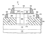
- Features depicted in FIG. 7 include a source element 450 , a gate element 320 , and sidewall elements 460 and 470 .
- the source element 450 and the gate element 320 are formed with a poly etch process well known in the art of semiconductor processing.
- the etching action removes the portion of layer 500 that is not protected by the photoresist pattern 510 and the portion of layer 300 that is not protected by oxide element 410 and nitride element 420 .
- Element 470 and element 460 are referred in the art of semiconductor processing as the sidewalls. They are formed by a technique combining a film deposition and a film etching.
- the etching action not only removes the newly deposited film but also a portion of the oxide element 410 and nitride element 420 that is not covered by the source element 450 or the sidewall elements 460 and 460 .
- the silicon surfaces of the source element 450 and the gate element 320 are uncovered.
- FIG. 7 also depicts the source and gate implant processes.
- the gate-implant species is boron
- the dose is 3 ⁇ 10 15 ions/cm 2
- the implant energy is 20 keV.
- the source implant species is arsenic
- the dose is 1.5 ⁇ 10 15 ions/cm 2
- the implant energy is 50 keV.
- Other implant species, dosages and energies maybe used to effect low resistivity in the source and gate-poly-regions.
- the JFET embodying this invention has a “vertical” channel.
- the “vertical” channel in the present invention channels the flow of the charge carriers in a direction substantially perpendicular to the “surface” of the semiconductor surface.
- the interaction between the charge carrier and the surface imperfection is substantially reduced, which enables the JFETs embodying this invention to have superior cutoff frequency (f co ) and 1/f noise figure.
Landscapes
- Engineering & Computer Science (AREA)
- Microelectronics & Electronic Packaging (AREA)
- Power Engineering (AREA)
- Physics & Mathematics (AREA)
- Ceramic Engineering (AREA)
- Condensed Matter Physics & Semiconductors (AREA)
- General Physics & Mathematics (AREA)
- Computer Hardware Design (AREA)
- Manufacturing & Machinery (AREA)
- Junction Field-Effect Transistors (AREA)
- Metal-Oxide And Bipolar Metal-Oxide Semiconductor Integrated Circuits (AREA)
- Thin Film Transistor (AREA)
Abstract
We disclose the structure of an electronic device, the method of making the device and the operation of the device. The device is built near the top of a substrate. It has, near the top surface, a buried layer that is electrically communicable to a drain terminal. The device has a body region over the buried layer. A portion of the body region contacts a gate region connected to a gate terminal. The device has a channel region, of which the length spans the distance between the buried layer and a source region, which projects upward from the channel region and is connected to a source terminal. The device current flows in the channel substantially perpendicularly to the top surface of the substrate.
Description
This invention relates to semiconductor devices and particularly to an improved junction field effect transistor (JFET).
A conventional JFET is a three-terminal semiconductor device in which a current flowing substantially parallel to the top surface of the semiconductor chip is controlled by an externally applied vertical electric field, as shown in FIG. 1 a, 1 b, and 1 c. It can be used as a switch or an amplifier. JFET is known as the unipolar transistor because the current is transported by carriers of one polarity, namely, the majority carriers. This is in contrast with the bipolar junction transistor, in which both majority-and-minority-carrier currents are important.
A typical n-channel JFET fabricated by the standard planar process is shown in FIG. 1. FIG. 1 a depicts a JFET built in a semiconductor substrate in an epitaxial layer. FIG. 1 b depicts a JFET fabricated by a double-diffused technique in a bulk semiconductor substrate. FIG. 1 c is a schematic representation of both JFETs.
The active region of the JFET consists of a lightly doped n-type channel sandwiched between two heavily doped p+-gate regions. In FIG. 1 a, the lower p+ region is the substrate, and the upper p+ region is formed by boron diffusion into the epitaxially grown n-type channel. The p+ regions are connected either internally or externally to form the gate terminal. Ohmic contacts attached to the two ends of the channel are known as the drain and source terminals through which the channel current flows. Alternatively, the JFET may be fabricated by the double-diffused technique with a diffused channel and an upper gate as illustrated in FIG. 1 b. In both cases, the channel and the gate regions run substantially parallel the top surface of the substrate, so does the current flow in the channel.
When a JFET operates as a switch, without a gate bias voltage, the transistor has a conducting channel between the source and the drain terminals. This is the ON state. To reach the OFF state, a reverse-biasing gate voltage is applied to deplete all carriers in the channel.
The reverse voltage bias applied across the gate/channel junctions depletes free carriers from the channel and produces space-charge regions extending into the channel. With a gate voltage set between ON and OFF levels, the cross-sectional area of the channel and the channel resistance can be varied. Thus the current flow between the source and the drain is modulated by the gate voltage.
An important figure of merit of a JFET is its cutoff frequency (fco), which can be represented mathematically as follows:
f co ≦qa 2μn N d/(4πk∈o L 2),
where q is the electric charge of the charge carriers, a is the channel width, μn is the mobility of the charge carriers, Nd is the doping concentration in the channel, k and ∈o are the dielectric constant and the electrical permittivity of the semiconductor material and the free space respectively, and L is the channel length.
Another important figure of merit of a JFET is the noise figure. At lower frequencies the dominant noise source in a transistor is due to the interaction of the current flow and the surface region that gives rise to the 1/f noise spectrum.
This invention provides a JFET device that has superior fco and 1/f performance over conventional JFETs and a process of making the device.
In FIG. 2 , an n-channel JFET 10 is shown as a three-terminal device, fabricated near the surface of a semiconductor substrate surface. The semiconductor material in the preferred embodiment is silicon. A JFET embodying this invention can also be fabricated in other semiconductor materials such as germanium, germanium-silicon, gallium arsenide or other compound material. FIG. 2 depicts a JFET built in a bulk silicon substrate. A JFET embodying this invention can also be fabricated in a substrate of semiconductor-on-insulator such as SIMOX, silicon-on-sapphire, or in bonded wafer. FIG. 2 depicts an n-channel JFET. A JFET embodying this invention can also be implemented as a p-channel JFET. A JFET may also be one device in an integrated circuit that includes CMOS and Bipolar circuit elements, and passive circuit components.
The substrate 110 may be either n-type or p-type. In a typical integrated circuit fabricated by a BiCMOS process, the substrate 110 would be a lightly doped, p-type crystalline silicon material. Over a portion of the substrate 110 is an n-type layer 150 of low resistivity that constitutes the drain portion of the JFET. In a BiCMOS structure, a region commonly referred to as “a buried layer” fits this requirement.
Over a portion of the buried layer 150 is layer 200. Layer 200 includes several regions of different materials. Among them, region 220 includes primarily dielectric material. In this embodiment, this material is silicon dioxide, fabricated with a STI technique. Region 220 may also be built with a LOCOS technique or other techniques well known in the art. Element 210 of layer 200 is substantially p-type mono-crystalline silicon. It may be formed by an epitaxial technique.
The channel may be created by implanting n-type ions perpendicular to the substrate surface. The dopant concentration in the channel region is usually not uniform. In fact, it is advantageous to be able to tailor the doping profile, for example, so that the dopant concentration in the channel region near the surface of the substrate is lower than the dopant concentration distant from the surface of the substrate. This dopant profile places the pinch-off region closer to the top of layer 310 and uses the shallow portion of the implanted ions to set the pinch-off voltage of the JFET. Such a profile may be accomplished with a multiple-implant process. The multiple implants may be of various dosages and implant energies. In this embodiment, we employ a three-implant process—one at 220 keV, one at 340 keV and one at 500 keV.
The source region 450 in this embodiment is poly-crystalline. It makes contact to the channel region 350 through an opening 415 etched out through an insulating element that comprises a silicon dioxide element 410 and a silicon nitride element 420. In the preferred embodiment, there is an absence of native oxide between the source region 450 and the channel region 350 so the source region contacts the channel region and the silicon immediately above the channel region may retain the mono-crystalline structure within a short range. In another embodiment, minute oxide may exist in the vicinity of the opening 450 as result of chemical processes such as a wet chemical cleanup process. The source region 450 is heavily doped with phosphorus, arsenic, or other n-type dopants and it partially overhangs the gate regions 320 and is insulated from the gate region 320 by silicon dioxide elements 410, silicon nitride elements 420, oxide elements 460 and nitride elements 470.
The portion of epi-layer 300 that is in contact with element 210 is mono-crystalline while the portion that contacts element 220 is poly-crystalline.
The region 350 is the n-channel region of the JFET, it maybe formed by implanting n-type ions into region 210 through the opening 415. In this embodiment, the channel is formed with a three-step ion-implant process. One implant is at 200 keV, another implant is at 340 keV, and another implant is at 500 keV. Dosages of phosphorus ions that may range from 2×10⁹ to 4×10¹¹ ions/cm2 per implant are used in the 3-step implant—with the higher energy implants typically associate with higher doses. Other n-type ion species and implant dosages and energies may also be used to tailor the channel doping profile to suit specific circuit requirement.
In this embodiment, the source element 450 and the gate element 320 are formed with a poly etch process well known in the art of semiconductor processing. The etching action removes the portion of layer 500 that is not protected by the photoresist pattern 510 and the portion of layer 300 that is not protected by oxide element 410 and nitride element 420. Element 470 and element 460 are referred in the art of semiconductor processing as the sidewalls. They are formed by a technique combining a film deposition and a film etching. The etching action not only removes the newly deposited film but also a portion of the oxide element 410 and nitride element 420 that is not covered by the source element 450 or the sidewall elements 460 and 460. At the completion of the etching process, the silicon surfaces of the source element 450 and the gate element 320 are uncovered.
Contrary to conventional JFETs, as depicted in FIGS. 1 a, 1 b, and 1 c, which have their channel substantially parallel and proximate to the top surface of the semiconductor substrate, the JFET embodying this invention has a “vertical” channel.
It is well known in the art of semiconductor physics that the top surface of the semiconductor substrate is heavily populated with imperfections such as charge traps and surface states. The interaction between the charge carrier in the channel and the surface imperfections is partially responsible for the performance limitation of conventional semiconductor devices in which the current flows parallel to and near the surface.
In contrast, the “vertical” channel in the present invention channels the flow of the charge carriers in a direction substantially perpendicular to the “surface” of the semiconductor surface. Thus the interaction between the charge carrier and the surface imperfection is substantially reduced, which enables the JFETs embodying this invention to have superior cutoff frequency (fco) and 1/f noise figure.
Claims (23)
1. An electronic device, comprising
a. a substrate, having a top surface and a bottom surface;
b. a buried layer near the top surface, electrically communicable to a drain terminal;
c. a body region, having a second top surface, a second bottom surface and a second side surface, a portion of the side surface contacting a gate region communicable to a gate terminal;
d. a channel region, having a third top surface, a third bottom surface, and a third side surface, the third side surface contacting the body region, the third bottom surface being substantially coplanar to the second bottom surfaces and contacting the buried layer, the third top surface being substantially coplanar to the second top surface and electrically communicable to a source region; and
e. the source region, projecting upward from the channel region, electrically communicable to a source terminal.
2. The electronic device in claim 1 in which the substrate is a semiconductor material.
3. The electronic device in claim 2 in which the semiconductor material is p-type silicon.
4. The electronic device in claim 1 in which the buried layer is n-type silicon material communicable to a drain terminal near the top surface through a sinker.
5. The electronic device in claim 1 in which the body region comprises two layers of substantially mono-crystalline p-type silicon layers.
6. The electronic device in claim 1 in which a portion of the body region contacts a dielectric region.
7. The electronic device in claim 6 in which the dielectric region comprises a silicon dioxide region formed with a STI technique.
8. The electronic device in claim 1 in which the channel region comprises of three groups of n-type dopant ions distributed along a direction perpendicular to the top surface of the substrate.
9. The electronic device in claim 1 in which the dopant ion distribution in the channel region is lighter near the source region than near the drain region.
10. The electronic device in claim 1 in which the gate region is substantially p-type polycrystalline silicon.
11. The electronic device in claim 1 , in which an electrical current flows in the channel region upon a voltage bias being applied between the source terminal and the drain terminal.
12. The electronic device in claim 11 , in which the electrical current flows in a direction substantially perpendicular the top surface of the substrate.
13. The electronic device in claim 11 , in which the magnitude of the current is a function of a voltage at the gate terminal.
14. The electronic device in claim 1 , in which the channel region is doped with n-type dopant.
15. The electronic device in claim 1 , in which the channel region is doped with p-type dopant.
16. A semiconductor integrated circuit device, comprising
a. a semiconductor substrate, having a top surface and a bottom surface;
b. a buried layer of crystalline semiconductor material near the top surface, doped with a dopant of a first polarity, electrically communicable to a drain terminal near the top surface;
c. a mono-crystalline first region, doped with dopant of the first polarity, having a top surface, a bottom surface and a side surface, the lower portion of the side surface contacting an electrically insulating region and the upper portion of the side surface coupling to a gate region communicable to a gate terminal near the top surface of the substrate;
d. a channel region, doped with dopant of a second polarity, having a top surface, a bottom surface, and a side surface, the top surface being substantially coplanar to the top surface of the first region, the bottom surface being substantially coplanar to the bottom surfaces of the first region and electrically communicable to the buried layer, the side surface contacting the first region; and
e. a source region, projecting upward from the channel region, having a top surface electrically communicable to a source terminal, a bottom surface electrically communicable to the top surface of the channel region.
17. The electronic device in claim 16 , in which an electrical current flows in the channel region upon a voltage bias being applied between the source terminal and the drain terminal.
18. The electronic device in claim 17 , in which the electrical current flows in a direction substantially perpendicular the top surface of the substrate.
19. The electronic device in claim 17 , in which the magnitude of the current is a function of a voltage at the gate terminal.
20. The electronic device in claim 16 , in which the distance between the top surface and the bottom surface of the channel region is about 0.7 micro-meters, in which about 0.5 micro-meter is attributable to a bottom layer and about 0.2 micro-meters is attributable to a top layer.
21. The electronic device in claim 16 , in which the dopant of a first polarity is p-type.
22. The electronic device in claim 16 , in which the dopant of a first polarity is n-type.
23. An n-channel silicon JFET, comprising
a. a silicon substrate, having a top surface and a bottom surface;
b. a buried layer of mono-crystalline silicon near the top surface, doped with a n-type dopant to a sheet resistance of about 25 ohms per square, the buried layer being electrically communicable to a drain terminal near the top surface of the substrate;
c. a silicon mono-crystalline first region, doped with p-type dopant to a concentration of about 1×10¹⁵ dopant ions per cubic centimeter, having a top surface, a bottom surface and a side surface, the distance between the top and the bottom surfaces being about 0.7 micrometers, the lower portion of the side surface being in contact with a silicon dioxide region and the upper portion of the side surface being in contact with a p-type, poly-crystalline silicon gate region;
d. the silicon gate region being communicable to a gate terminal near the top surface of the substrate;
e. an n-type silicon mono-crystalline-channel region, doped with n-type dopant to a concentration higher than about 1×10¹⁵ dopant ions per cubic centimeter, having a top surface, a bottom surface, and a side surface, the top surface being substantially coplanar to the top surface of the p-type first region, the bottom surface being substantially coplanar to the bottom surfaces of the p-type region in c and electrically communicable to the buried layer, the side surface contacting the p-type first region;
f. a first n-type, poly-crystalline-silicon-source region, projecting upward from the channel region and the gate region, having a top surface electrically communicable to a source terminal near the top surface of the substrate, a bottom surface electrically communicable to the top surface of the channel region, a side surface in contact with dielectric sidewall spacers;
g. the first n-type, poly-crystalline-silicon-source region in f being electrically insulated from the first p-type, poly-crystalline-silicon-gate region.
h. the device being operable channeling an electrical current through the channel region upon a voltage bias being applied between the source terminal and the drain terminal; and
i. the electrical current flowing in a direction substantially perpendicular the top surface of the silicon substrate, the magnitude of the electrical current being a function of a voltage at the gate terminal.
Priority Applications (2)
| Application Number | Priority Date | Filing Date | Title |
|---|---|---|---|
| US10/614,840 US6909125B2 (en) | 2003-07-08 | 2003-07-08 | Implant-controlled-channel vertical JFET |
| US11/127,991 US20050247955A1 (en) | 2003-07-08 | 2005-05-11 | Implant-controlled-channel vertical JFET |
Applications Claiming Priority (1)
| Application Number | Priority Date | Filing Date | Title |
|---|---|---|---|
| US10/614,840 US6909125B2 (en) | 2003-07-08 | 2003-07-08 | Implant-controlled-channel vertical JFET |
Related Child Applications (1)
| Application Number | Title | Priority Date | Filing Date |
|---|---|---|---|
| US11/127,991 Division US20050247955A1 (en) | 2003-07-08 | 2005-05-11 | Implant-controlled-channel vertical JFET |
Publications (2)
| Publication Number | Publication Date |
|---|---|
| US20050006663A1 US20050006663A1 (en) | 2005-01-13 |
| US6909125B2 true US6909125B2 (en) | 2005-06-21 |
Family
ID=33564432
Family Applications (2)
| Application Number | Title | Priority Date | Filing Date |
|---|---|---|---|
| US10/614,840 Expired - Lifetime US6909125B2 (en) | 2003-07-08 | 2003-07-08 | Implant-controlled-channel vertical JFET |
| US11/127,991 Abandoned US20050247955A1 (en) | 2003-07-08 | 2005-05-11 | Implant-controlled-channel vertical JFET |
Family Applications After (1)
| Application Number | Title | Priority Date | Filing Date |
|---|---|---|---|
| US11/127,991 Abandoned US20050247955A1 (en) | 2003-07-08 | 2005-05-11 | Implant-controlled-channel vertical JFET |
Country Status (1)
| Country | Link |
|---|---|
| US (2) | US6909125B2 (en) |
Cited By (2)
| Publication number | Priority date | Publication date | Assignee | Title |
|---|---|---|---|---|
| US20070080400A1 (en) * | 2003-09-29 | 2007-04-12 | Texas Instruments Incorporated | Low Noise Vertical Variable Gate Control Voltage JFET Device in a BiCMOS Process and Methods to Build this Device |
| US20070275515A1 (en) * | 2006-05-25 | 2007-11-29 | Texas Instruments Incorporated | Deep buried channel junction field effect transistor (DBCJFET) |
Families Citing this family (5)
| Publication number | Priority date | Publication date | Assignee | Title |
|---|---|---|---|---|
| US6812105B1 (en) * | 2003-07-16 | 2004-11-02 | International Business Machines Corporation | Ultra-thin channel device with raised source and drain and solid source extension doping |
| US6861678B2 (en) * | 2003-07-18 | 2005-03-01 | Texas Instruments Incorporated | Double diffused vertical JFET |
| US7084441B2 (en) * | 2004-05-20 | 2006-08-01 | Cree, Inc. | Semiconductor devices having a hybrid channel layer, current aperture transistors and methods of fabricating same |
| US7772056B2 (en) * | 2007-06-18 | 2010-08-10 | University Of Utah Research Foundation | Transistors for replacing metal-oxide semiconductor field-effect transistors in nanoelectronics |
| CN114678419A (en) * | 2022-05-27 | 2022-06-28 | 深圳平创半导体有限公司 | Semiconductor device and manufacturing method thereof, power switch device and power amplifier device |
Citations (4)
| Publication number | Priority date | Publication date | Assignee | Title |
|---|---|---|---|---|
| US6049108A (en) * | 1995-06-02 | 2000-04-11 | Siliconix Incorporated | Trench-gated MOSFET with bidirectional voltage clamping |
| US6392271B1 (en) * | 1999-06-28 | 2002-05-21 | Intel Corporation | Structure and process flow for fabrication of dual gate floating body integrated MOS transistors |
| US6518112B2 (en) * | 1998-01-05 | 2003-02-11 | International Business Machines Corporation | High performance, low power vertical integrated CMOS devices |
| US6825531B1 (en) * | 2003-07-11 | 2004-11-30 | Micrel, Incorporated | Lateral DMOS transistor with a self-aligned drain region |
Family Cites Families (1)
| Publication number | Priority date | Publication date | Assignee | Title |
|---|---|---|---|---|
| US6861678B2 (en) * | 2003-07-18 | 2005-03-01 | Texas Instruments Incorporated | Double diffused vertical JFET |
-
2003
- 2003-07-08 US US10/614,840 patent/US6909125B2/en not_active Expired - Lifetime
-
2005
- 2005-05-11 US US11/127,991 patent/US20050247955A1/en not_active Abandoned
Patent Citations (4)
| Publication number | Priority date | Publication date | Assignee | Title |
|---|---|---|---|---|
| US6049108A (en) * | 1995-06-02 | 2000-04-11 | Siliconix Incorporated | Trench-gated MOSFET with bidirectional voltage clamping |
| US6518112B2 (en) * | 1998-01-05 | 2003-02-11 | International Business Machines Corporation | High performance, low power vertical integrated CMOS devices |
| US6392271B1 (en) * | 1999-06-28 | 2002-05-21 | Intel Corporation | Structure and process flow for fabrication of dual gate floating body integrated MOS transistors |
| US6825531B1 (en) * | 2003-07-11 | 2004-11-30 | Micrel, Incorporated | Lateral DMOS transistor with a self-aligned drain region |
Non-Patent Citations (2)
| Title |
|---|
| Pending U.S. Appl. No. 10/623,230 (TI-35213), Howard et al. "Double Diffused Vertical JFET". |
| Pending U.S. Appl. No. 10/678,028 (TI-33654), Pendharkar et al. "A Low Noise Vertical Variable Gate Control Voltage JFET Device in a BICMOS Process & Methods to Build this Device". |
Cited By (4)
| Publication number | Priority date | Publication date | Assignee | Title |
|---|---|---|---|---|
| US20070080400A1 (en) * | 2003-09-29 | 2007-04-12 | Texas Instruments Incorporated | Low Noise Vertical Variable Gate Control Voltage JFET Device in a BiCMOS Process and Methods to Build this Device |
| US7598547B2 (en) | 2003-09-29 | 2009-10-06 | Texas Instruments Incorporated | Low noise vertical variable gate control voltage JFET device in a BiCMOS process and methods to build this device |
| US20070275515A1 (en) * | 2006-05-25 | 2007-11-29 | Texas Instruments Incorporated | Deep buried channel junction field effect transistor (DBCJFET) |
| US7348228B2 (en) | 2006-05-25 | 2008-03-25 | Texas Instruments Incorporated | Deep buried channel junction field effect transistor (DBCJFET) |
Also Published As
| Publication number | Publication date |
|---|---|
| US20050247955A1 (en) | 2005-11-10 |
| US20050006663A1 (en) | 2005-01-13 |
Similar Documents
| Publication | Publication Date | Title |
|---|---|---|
| US4700461A (en) | Process for making junction field-effect transistors | |
| US7598547B2 (en) | Low noise vertical variable gate control voltage JFET device in a BiCMOS process and methods to build this device | |
| JP3447927B2 (en) | Semiconductor device and manufacturing method thereof | |
| US5627395A (en) | Vertical transistor structure | |
| EP0537684B1 (en) | Improved performance lateral double-diffused MOS transistor and method of fabrication thereof | |
| US5349225A (en) | Field effect transistor with a lightly doped drain | |
| US6426279B1 (en) | Epitaxial delta doping for retrograde channel profile | |
| JP5378635B2 (en) | Metal oxide semiconductor device formed in silicon-on-insulator | |
| US6177299B1 (en) | Transistor having substantially isolated body and method of making the same | |
| US6579750B1 (en) | Manufacturing method for fully depleted silicon on insulator semiconductor device | |
| US20080036009A1 (en) | JFET with built in back gate in either SOI or bulk silicon | |
| US20050194621A1 (en) | Double diffused vertical JFET | |
| US11329156B2 (en) | Transistor with extended drain region | |
| US20050247955A1 (en) | Implant-controlled-channel vertical JFET | |
| US4914491A (en) | Junction field-effect transistors formed on insulator substrates | |
| EP1402580A1 (en) | Symmetric trench mosfet device and method of making same | |
| WO2003003452A2 (en) | Field-effect transistor and method of making the same | |
| CN109817714A (en) | Lateral double diffusion metal oxide semiconductor (LDMOS) device | |
| US6930357B2 (en) | Active SOI structure with a body contact through an insulator | |
| US20020014664A1 (en) | Multi-function semiconductor structure and method | |
| US5877047A (en) | Lateral gate, vertical drift region transistor | |
| US5925916A (en) | Semiconductor processing method of providing electrical isolation between adjacent semiconductor diffusion regions of different field effect transistors and integrated circuitry having adjacent electrically isolated field effect transistors | |
| US6420767B1 (en) | Capacitively coupled DTMOS on SOI | |
| KR20030084997A (en) | Soi devices with integrated gettering structure | |
| US6359298B1 (en) | Capacitively coupled DTMOS on SOI for multiple devices |
Legal Events
| Date | Code | Title | Description |
|---|---|---|---|
| AS | Assignment |
Owner name: TEXAS INSTRUMENTS INCORPORATED, TEXAS Free format text: ASSIGNMENT OF ASSIGNORS INTEREST;ASSIGNORS:HOWARD, GREGORY E.;SWANSON, LELAND S.;REEL/FRAME:014296/0856 Effective date: 20030702 |
|
| STCF | Information on status: patent grant |
Free format text: PATENTED CASE |
|
| FPAY | Fee payment |
Year of fee payment: 4 |
|
| FPAY | Fee payment |
Year of fee payment: 8 |
|
| FPAY | Fee payment |
Year of fee payment: 12 |