US6919784B2 - High cycle MEMS device - Google Patents
High cycle MEMS device Download PDFInfo
- Publication number
- US6919784B2 US6919784B2 US10/191,812 US19181202A US6919784B2 US 6919784 B2 US6919784 B2 US 6919784B2 US 19181202 A US19181202 A US 19181202A US 6919784 B2 US6919784 B2 US 6919784B2
- Authority
- US
- United States
- Prior art keywords
- pad
- switch
- conductive
- signal line
- actuation
- Prior art date
- Legal status (The legal status is an assumption and is not a legal conclusion. Google has not performed a legal analysis and makes no representation as to the accuracy of the status listed.)
- Expired - Fee Related, expires
Links
Images


Classifications
-
- H—ELECTRICITY
- H01—ELECTRIC ELEMENTS
- H01H—ELECTRIC SWITCHES; RELAYS; SELECTORS; EMERGENCY PROTECTIVE DEVICES
- H01H59/00—Electrostatic relays; Electro-adhesion relays
- H01H59/0009—Electrostatic relays; Electro-adhesion relays making use of micromechanics
-
- H—ELECTRICITY
- H01—ELECTRIC ELEMENTS
- H01H—ELECTRIC SWITCHES; RELAYS; SELECTORS; EMERGENCY PROTECTIVE DEVICES
- H01H1/00—Contacts
- H01H1/0036—Switches making use of microelectromechanical systems [MEMS]
- H01H2001/0084—Switches making use of microelectromechanical systems [MEMS] with perpendicular movement of the movable contact relative to the substrate
-
- H—ELECTRICITY
- H01—ELECTRIC ELEMENTS
- H01H—ELECTRIC SWITCHES; RELAYS; SELECTORS; EMERGENCY PROTECTIVE DEVICES
- H01H59/00—Electrostatic relays; Electro-adhesion relays
- H01H59/0009—Electrostatic relays; Electro-adhesion relays making use of micromechanics
- H01H2059/0072—Electrostatic relays; Electro-adhesion relays making use of micromechanics with stoppers or protrusions for maintaining a gap, reducing the contact area or for preventing stiction between the movable and the fixed electrode in the attracted position
Definitions
- the field of the invention is micro-electromechanical systems (MEMS).
- MEMS devices are macroscale devices including a pad that is movable in response to electrical signaling.
- the movable pad such as a membrane or cantilevered metal arm, moves in response to an electrical signal to cause an electrical effect.
- a membrane variable capacitor is a membrane variable capacitor.
- the membrane deforms in response to an electrical signal.
- the membrane itself is part of a capacitor, and the distance between the membrane and another portion of the capacitor changes the capacitance.
- Another MEMS device is an RF (radio frequency) ohmic switch.
- RF radio frequency
- application of an electrical signal causes a cantilevered metal arm to either ground or remove from ground state a signal line by completing or breaking ohmic contact with the signal line.
- Dielectric layers in MEMS devices are used to prevent the membrane, cantilevered arm, or other moving switch pad from making physical contact with other portions of the MEMS device.
- a common cause of failure is a stuck switch pad, recognized by experience to be the sticking of the movable switch pad to a dielectric layer. The exact mechanisms for this sticking are not completely understood. Sticking has been attributed to charging of dielectric layers used to isolate electrical contact between the moving switch pad of a MEMS device and an actuation component of the MEMS device. Another common cause of failure and operational inefficiency is the tendency of the switch pad to deform due to spring force. It can move further away from an actuation pad, first leading to an increased voltage required for operation of the switch and eventually leading to a failure.
- a high life cycle MEMS device is provided by the invention.
- separate support posts are disposed to prevent a suspended switch pad from touching the actuation pad while permitting the switch pad to ground a signal line.
- cantilevered support beams are made from a thicker material than the switching pad. Thicker material in the cantilever tends to keep the switch pad flat in its resting position.
- features of particular preferred embodiments include dimples in the switch pad to facilitate contact with a signal line and serpentine cantilevers arranged symmetrically to support the switch pad.
- FIG. 1 is a schematic of a preferred embodiment RF MEMS shunt switch
- FIGS. 2A and 2B are SEM images of the cantilever portion of a prototype device of the invention.
- FIG. 4 is an SEM image of a center portion of a prototype device of the invention.
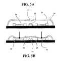
- FIG. 5A is a schematic side view of a preferred embodiment MEMS switch of the invention in a relaxed (ungrounded) state
- FIG. 5B is a schematic side view of the FIG. 5A switch in an actuated (grounded) state
- FIG. 6 is an SEM image of a support post feature of a prototype device of the invention.
- aspects of the invention are directed generally to the cycle life, manufacturing yield, and electrical efficiency of MEMS devices, e.g., shunt switches.
- aspects of the invention produce electrical efficiency, i.e., low voltage operation, by addressing the issues of residual stress and electrical contact in the switch.
- the residual stress in the switch adversely affects the required actuation voltage by causing the switch to bend such that the distance between it and the signal path increases.
- Cantilevered support of a moving switch pad in the invention provides for a strong return-to-flat tendency. As a distance between an actuation pad and a moving switch pad is maintained, a consistent and low actuation voltage is possible.
- Cycle life and, to some extent, electrical efficiency are also addressed by an aspect of the invention that permits an exposed actuation pad.
- FIG. 1 a preferred embodiment RF MEMS shunt switch is shown.
- the function of the RF MEMS switch of FIG. 1 is to control a signal line 10 to selectively permit the flow of signals through the signal line 10 in response to a control signal. Signal flow is permitted when a metal switch pad 12 suspended over the signal line 10 is not in contact with the signal line 10 .
- the relaxed state of the switch is the state when signal flow is permitted to pass through the signal line 10 .
- cantilevers 14 hold the metal switch pad 12 above the signal line 10 .
- Application of a control signal to an actuation pad (or pads) 16 will ground the signal line 10 by pulling the metal switch pad 12 into contact with the signal line 10 and a ground 18 .
- cantilevers 14 are arranged to create a balanced switch.
- the cantilevers 14 preferably have a serpentine shape and are arranged symmetrically to be disposed proximate corners of the metal switch pad 12 , which, in the preferred embodiment, has a generally rectangular shape. With other shaped metal switch pads, symmetry is preferably maintained in the arrangement of the cantilevers 14 and will depend upon the shape.
- FIGS. 2A and 2B are SEM images of a prototype MEMS device of the invention. Magnification in FIG. 2B is greater than in FIG. 2 A.
- An additional selective deposition process is used to thicken the cantilevers after an initial deposition process forms the cantilevers 14 and the metal switch pad 12 .
- the thickened cantilevers 14 have increased mechanical strength. Their higher spring constant provides a restoring force that keeps the switch flat.
- the metal switch pad 12 has a thickness in the approximate range of 0.1 ⁇ m to 3 ⁇ m, and the cantilevers 14 have an additional thickness in the approximate range of 0.3 ⁇ m to 1.5 ⁇ m.
- a particularly preferred embodiment has cantilevers with an additional 0.75 ⁇ m to 1.0 ⁇ m thickness.
- FIG. 3 is a schematic side view illustrating, in exaggerated fashion, a dimpled metal switch pad 20 and FIG. 4 is an SEM image of a metal switch pad portion of a prototype including a dimpled metal switch pad.
- a dimple 22 is formed over the signal line 10 , but may also be aligned with the grounds 18 .
- the dimple 22 is created by partially etching the sacrificial layer upon which the metal switch pad 12 is formed. The partial etching creates a depression. The dimple 22 is formed in the depression when the metal actuation pad 20 is formed.
- the metal actuation pad with dimple or dimples is then released upon consumption of the sacrificial layer.
- the effect is that the center portion of the metal switch pad 20 is lowered at the dimple 22 such that when the metal switch pad 20 is pulled down the first thing to contact the signal line 10 is the dimple 22 .
- the basic FIG. 3 structure also provides for a variable capacitor when the range of the pull down of the metal switch pad 20 does not include contact with the signal line 10 .
- the dimpling is an efficient way to create variable capacitors by adjusting the dimple depth and thereby not making contact to the signal line. Changing the gap between signal and ground changes the capacitance through an actuation voltage applied in an actuation pad 24 .
- FIG. 3 also illustrates support posts 26 , shown in additional detail in FIGS. 5A and 5B , and raised contact bumps 28 to the signal line 10 and ground 18 .
- the support posts 26 are disposed to prevent the metal switch pad 12 from contacting the actuation pads 16 .
- the actuation pad 24 may include a dielectric, or may be an exposed metal.
- the raised contact bump 28 facilitates electrical contact and reduces the gap between it and the dimple 22 .
- the support posts 26 in FIGS. 5A and 5B are disposed around the actuation pad 12 and are high enough to stop the metal switch pad before it contacts the actuation pads.
- the posts 26 are preferably disposed on multiple sides of the actuation pads 16 and are preferably fabricated close to the actuation pads 16 .
- the support posts 26 may be formed to ground contact. In this way, the posts 26 will direct some current from the signal line 10 to ground, with the remainder being directed through the cantilevers 14 .
- Posts are shown in the partial SEM image of a prototype in FIG. 6 .
- posts In a preferred low voltage embodiments, posts have a height in the approximate range of 0.5 to 1.25 ⁇ m and an actuation pad (with dielectric) is approximately 1000 ⁇ to 2000 ⁇ .
- Some applications, e.g., wireless RF devices permit higher actuation voltages. In such applications, higher posts are preferred to enhance lifetimes.
- a preferred range for the posts in such devices is 0.5 ⁇ m to 100 ⁇ m with an actuation pad of approximately 1000 ⁇ to 2000 ⁇ .
Abstract
Description
Claims (19)
Priority Applications (3)
| Application Number | Priority Date | Filing Date | Title |
|---|---|---|---|
| US10/191,812 US6919784B2 (en) | 2001-10-18 | 2002-07-09 | High cycle MEMS device |
| PCT/US2002/031088 WO2003034457A2 (en) | 2001-10-18 | 2002-10-01 | High cycle mems device |
| US10/868,130 US7142076B2 (en) | 2001-10-18 | 2004-06-14 | High cycle MEMS device |
Applications Claiming Priority (2)
| Application Number | Priority Date | Filing Date | Title |
|---|---|---|---|
| US33040501P | 2001-10-18 | 2001-10-18 | |
| US10/191,812 US6919784B2 (en) | 2001-10-18 | 2002-07-09 | High cycle MEMS device |
Related Child Applications (1)
| Application Number | Title | Priority Date | Filing Date |
|---|---|---|---|
| US10/868,130 Division US7142076B2 (en) | 2001-10-18 | 2004-06-14 | High cycle MEMS device |
Publications (2)
| Publication Number | Publication Date |
|---|---|
| US20040008099A1 US20040008099A1 (en) | 2004-01-15 |
| US6919784B2 true US6919784B2 (en) | 2005-07-19 |
Family
ID=26887421
Family Applications (2)
| Application Number | Title | Priority Date | Filing Date |
|---|---|---|---|
| US10/191,812 Expired - Fee Related US6919784B2 (en) | 2001-10-18 | 2002-07-09 | High cycle MEMS device |
| US10/868,130 Expired - Fee Related US7142076B2 (en) | 2001-10-18 | 2004-06-14 | High cycle MEMS device |
Family Applications After (1)
| Application Number | Title | Priority Date | Filing Date |
|---|---|---|---|
| US10/868,130 Expired - Fee Related US7142076B2 (en) | 2001-10-18 | 2004-06-14 | High cycle MEMS device |
Country Status (2)
| Country | Link |
|---|---|
| US (2) | US6919784B2 (en) |
| WO (1) | WO2003034457A2 (en) |
Cited By (10)
| Publication number | Priority date | Publication date | Assignee | Title |
|---|---|---|---|---|
| US20040069608A1 (en) * | 2002-07-30 | 2004-04-15 | Norisato Shimizu | Switch and method for manufacturing the same |
| US20040227599A1 (en) * | 2003-05-14 | 2004-11-18 | Jun Shen | Latachable, magnetically actuated, ground plane-isolated radio frequency microswitch and associated methods |
| US20070120438A1 (en) * | 2003-12-26 | 2007-05-31 | Commissariat A L'energie Atomique | Electrostatic control device |
| US20070170460A1 (en) * | 2005-12-08 | 2007-07-26 | Electronics And Telecommunications Research Institute | Micro-electro mechanical systems switch and method of fabricating the same |
| US20070215447A1 (en) * | 2004-04-06 | 2007-09-20 | Commissariat A L'energie Atomique | Low Consumption and Low Actuation Voltage Microswitch |
| US20090107813A1 (en) * | 2007-10-31 | 2009-04-30 | O'brien Kathleen Ann | System and method for avoiding contact stiction in micro-electromechanical system based switch |
| US20090272635A1 (en) * | 2008-05-01 | 2009-11-05 | Kenichiro Suzuki | Mems switch provided with movable electrode member supported through springs on substrate having bump |
| US20100001355A1 (en) * | 2008-07-07 | 2010-01-07 | Honeywell International Inc. | RF MEMS Switch |
| US20120279845A1 (en) * | 2011-04-11 | 2012-11-08 | Mark Bachman | Use of Micro-Structured Plate for Controlling Capacitance of Mechanical Capacitor Switches |
| US8461948B2 (en) | 2007-09-25 | 2013-06-11 | The United States Of America As Represented By The Secretary Of The Army | Electronic ohmic shunt RF MEMS switch and method of manufacture |
Families Citing this family (4)
| Publication number | Priority date | Publication date | Assignee | Title |
|---|---|---|---|---|
| US6876282B2 (en) * | 2002-05-17 | 2005-04-05 | International Business Machines Corporation | Micro-electro-mechanical RF switch |
| JP2009291030A (en) * | 2008-05-30 | 2009-12-10 | Toshiba Corp | Mems variable capacitor |
| CN110047662A (en) * | 2019-04-16 | 2019-07-23 | 苏州希美微纳系统有限公司 | A kind of high switching capacity ratio RF MEMS capacitive switch |
| CN113381139B (en) * | 2021-04-20 | 2023-05-02 | 中北大学 | K-D band broadband radio frequency MEMS switch |
Citations (17)
| Publication number | Priority date | Publication date | Assignee | Title |
|---|---|---|---|---|
| US4959515A (en) | 1984-05-01 | 1990-09-25 | The Foxboro Company | Micromechanical electric shunt and encoding devices made therefrom |
| US5168249A (en) | 1991-06-07 | 1992-12-01 | Hughes Aircraft Company | Miniature microwave and millimeter wave tunable circuit |
| US5258591A (en) | 1991-10-18 | 1993-11-02 | Westinghouse Electric Corp. | Low inductance cantilever switch |
| US5677823A (en) | 1993-05-06 | 1997-10-14 | Cavendish Kinetics Ltd. | Bi-stable memory element |
| US5929497A (en) | 1998-06-11 | 1999-07-27 | Delco Electronics Corporation | Batch processed multi-lead vacuum packaging for integrated sensors and circuits |
| US6046659A (en) | 1998-05-15 | 2000-04-04 | Hughes Electronics Corporation | Design and fabrication of broadband surface-micromachined micro-electro-mechanical switches for microwave and millimeter-wave applications |
| US6091050A (en) * | 1997-11-17 | 2000-07-18 | Roxburgh Limited | Thermal microplatform |
| US6100477A (en) | 1998-07-17 | 2000-08-08 | Texas Instruments Incorporated | Recessed etch RF micro-electro-mechanical switch |
| US6124650A (en) | 1999-10-15 | 2000-09-26 | Lucent Technologies Inc. | Non-volatile MEMS micro-relays using magnetic actuators |
| US6143997A (en) * | 1999-06-04 | 2000-11-07 | The Board Of Trustees Of The University Of Illinois | Low actuation voltage microelectromechanical device and method of manufacture |
| US6307452B1 (en) | 1999-09-16 | 2001-10-23 | Motorola, Inc. | Folded spring based micro electromechanical (MEM) RF switch |
| US6437965B1 (en) * | 2000-11-28 | 2002-08-20 | Harris Corporation | Electronic device including multiple capacitance value MEMS capacitor and associated methods |
| US20020171517A1 (en) | 2001-05-17 | 2002-11-21 | Institute Of Microelectronics | Inductor-capacitor resonant rf switch |
| US6535091B2 (en) * | 2000-11-07 | 2003-03-18 | Sarnoff Corporation | Microelectronic mechanical systems (MEMS) switch and method of fabrication |
| US6700172B2 (en) | 1998-11-25 | 2004-03-02 | Raytheon Company | Method and apparatus for switching high frequency signals |
| US20040050675A1 (en) * | 2002-09-17 | 2004-03-18 | The Board Of Trustees Of The University Of Illinois | High cycle cantilever MEMS devices |
| US6713695B2 (en) | 2002-03-06 | 2004-03-30 | Murata Manufacturing Co., Ltd. | RF microelectromechanical systems device |
Family Cites Families (5)
| Publication number | Priority date | Publication date | Assignee | Title |
|---|---|---|---|---|
| US20040005675A9 (en) * | 2000-01-13 | 2004-01-08 | Mike Farwick | Nucleotide sequences encoding the ptsH gene |
| JP3538109B2 (en) * | 2000-03-16 | 2004-06-14 | 日本電気株式会社 | Micro machine switch |
| US6529093B2 (en) * | 2001-07-06 | 2003-03-04 | Intel Corporation | Microelectromechanical (MEMS) switch using stepped actuation electrodes |
| US6657525B1 (en) * | 2002-05-31 | 2003-12-02 | Northrop Grumman Corporation | Microelectromechanical RF switch |
| US6686820B1 (en) * | 2002-07-11 | 2004-02-03 | Intel Corporation | Microelectromechanical (MEMS) switching apparatus |
-
2002
- 2002-07-09 US US10/191,812 patent/US6919784B2/en not_active Expired - Fee Related
- 2002-10-01 WO PCT/US2002/031088 patent/WO2003034457A2/en not_active Application Discontinuation
-
2004
- 2004-06-14 US US10/868,130 patent/US7142076B2/en not_active Expired - Fee Related
Patent Citations (17)
| Publication number | Priority date | Publication date | Assignee | Title |
|---|---|---|---|---|
| US4959515A (en) | 1984-05-01 | 1990-09-25 | The Foxboro Company | Micromechanical electric shunt and encoding devices made therefrom |
| US5168249A (en) | 1991-06-07 | 1992-12-01 | Hughes Aircraft Company | Miniature microwave and millimeter wave tunable circuit |
| US5258591A (en) | 1991-10-18 | 1993-11-02 | Westinghouse Electric Corp. | Low inductance cantilever switch |
| US5677823A (en) | 1993-05-06 | 1997-10-14 | Cavendish Kinetics Ltd. | Bi-stable memory element |
| US6091050A (en) * | 1997-11-17 | 2000-07-18 | Roxburgh Limited | Thermal microplatform |
| US6046659A (en) | 1998-05-15 | 2000-04-04 | Hughes Electronics Corporation | Design and fabrication of broadband surface-micromachined micro-electro-mechanical switches for microwave and millimeter-wave applications |
| US5929497A (en) | 1998-06-11 | 1999-07-27 | Delco Electronics Corporation | Batch processed multi-lead vacuum packaging for integrated sensors and circuits |
| US6100477A (en) | 1998-07-17 | 2000-08-08 | Texas Instruments Incorporated | Recessed etch RF micro-electro-mechanical switch |
| US6700172B2 (en) | 1998-11-25 | 2004-03-02 | Raytheon Company | Method and apparatus for switching high frequency signals |
| US6143997A (en) * | 1999-06-04 | 2000-11-07 | The Board Of Trustees Of The University Of Illinois | Low actuation voltage microelectromechanical device and method of manufacture |
| US6307452B1 (en) | 1999-09-16 | 2001-10-23 | Motorola, Inc. | Folded spring based micro electromechanical (MEM) RF switch |
| US6124650A (en) | 1999-10-15 | 2000-09-26 | Lucent Technologies Inc. | Non-volatile MEMS micro-relays using magnetic actuators |
| US6535091B2 (en) * | 2000-11-07 | 2003-03-18 | Sarnoff Corporation | Microelectronic mechanical systems (MEMS) switch and method of fabrication |
| US6437965B1 (en) * | 2000-11-28 | 2002-08-20 | Harris Corporation | Electronic device including multiple capacitance value MEMS capacitor and associated methods |
| US20020171517A1 (en) | 2001-05-17 | 2002-11-21 | Institute Of Microelectronics | Inductor-capacitor resonant rf switch |
| US6713695B2 (en) | 2002-03-06 | 2004-03-30 | Murata Manufacturing Co., Ltd. | RF microelectromechanical systems device |
| US20040050675A1 (en) * | 2002-09-17 | 2004-03-18 | The Board Of Trustees Of The University Of Illinois | High cycle cantilever MEMS devices |
Non-Patent Citations (9)
| Title |
|---|
| C. Goldsmith Z. Yao, S. Eshelman, D. Denniston, S. Chen, J. Ehmke, A. Malczewski, R. Richards, "Micromachining of RF Devices for Microwave Applications", Raytheon Tl Systems Materials, no date. |
| C. Goldsmith, J. Ehmke, A. Malczewski, B. Pillans, S. Eshelman, Z. Yao, J. Brank, and M. Eberly, "Lifetime Characterization of Capacitive RF Mems Switches", IEEE MTT-S 2001 International Microwave Symposium Digest, pp. 227-230, May 2001. |
| C.L. Goldsmith, Zhimin Yao, Susan Eshelman, and David Denniston, "Performance of Low-Loss RF MEMS Capacitive Switches" IEEE Microwave and Guides Wave Letters, vol. 8, No. 8, Aug. 1988, pp. 269-271. |
| Chuck Goldsmith, Tsen-Hwang Lin, Bill Powers, Wen-Rong Wu, Bill Norvell, "Micromechanical Membrane Switches for Microwave Applications", IEEE MTT-S Digest, 1995, pp. 91-94, no month. |
| Elliot R. Brown, "RF-MEMS Switches for Reconfigurable Integrated Circuits", IEEE Transactions on Microwave Theory and Techniques, vol. 46, No. 11, Nov. 1998, pp. 1868-1880. |
| J. Jason Yao, M. Frank Chang, "A Surface Micromachined Miniature Switch for Telecommunications Applications with Signal Frequencies from DC up to 4 GHZ", IEEE conference paper, 1995, no month. |
| J. Jason Yao, Sang Tae Park, and Jeffrey DeNatale, "High Tuning-Ratio MEMS-Based Tunable Capacitors for RF Communications Applications", Solid State Sensor and Actuator Workshop, Hilton Head Island, South Carolina, Jun. 8, 1998. |
| J.L. Ebel, A.P. Walker, R.E. Strawser, R. Cortez, K.D. Leedy, G.C. DeSalvo, "Investigation of MEMS RF switches for low loss phase shifters", GOMAC 2001 Digest of Papers, pp. 87-89, Mar. 2001. |
| N. Scott Barker, Gabriel M. Rebeiz, "Distributed MEMS True-Time Delay Phase Shifters and Wide-Bank Switches", IEEE Transactions on Microwave Theory and Techniques, vol. 46, No. 11, Nov. 1988, pp. 1881-1890. |
Cited By (16)
| Publication number | Priority date | Publication date | Assignee | Title |
|---|---|---|---|---|
| US20040069608A1 (en) * | 2002-07-30 | 2004-04-15 | Norisato Shimizu | Switch and method for manufacturing the same |
| US6992551B2 (en) * | 2002-07-30 | 2006-01-31 | Matsushita Electric Industrial Co., Ltd. | Switch and method for manufacturing the same |
| US20040227599A1 (en) * | 2003-05-14 | 2004-11-18 | Jun Shen | Latachable, magnetically actuated, ground plane-isolated radio frequency microswitch and associated methods |
| US7202765B2 (en) * | 2003-05-14 | 2007-04-10 | Schneider Electric Industries Sas | Latchable, magnetically actuated, ground plane-isolated radio frequency microswitch |
| US20070120438A1 (en) * | 2003-12-26 | 2007-05-31 | Commissariat A L'energie Atomique | Electrostatic control device |
| US7782170B2 (en) * | 2004-04-06 | 2010-08-24 | Commissariat A L'energie Atomique | Low consumption and low actuation voltage microswitch |
| US20070215447A1 (en) * | 2004-04-06 | 2007-09-20 | Commissariat A L'energie Atomique | Low Consumption and Low Actuation Voltage Microswitch |
| US7585113B2 (en) * | 2005-12-08 | 2009-09-08 | Electronics And Telecommunications Research Institute | Micro-electro mechanical systems switch and method of fabricating the same |
| US20070170460A1 (en) * | 2005-12-08 | 2007-07-26 | Electronics And Telecommunications Research Institute | Micro-electro mechanical systems switch and method of fabricating the same |
| US8461948B2 (en) | 2007-09-25 | 2013-06-11 | The United States Of America As Represented By The Secretary Of The Army | Electronic ohmic shunt RF MEMS switch and method of manufacture |
| US20090107813A1 (en) * | 2007-10-31 | 2009-04-30 | O'brien Kathleen Ann | System and method for avoiding contact stiction in micro-electromechanical system based switch |
| US7808764B2 (en) | 2007-10-31 | 2010-10-05 | General Electric Company | System and method for avoiding contact stiction in micro-electromechanical system based switch |
| US20090272635A1 (en) * | 2008-05-01 | 2009-11-05 | Kenichiro Suzuki | Mems switch provided with movable electrode member supported through springs on substrate having bump |
| US20100001355A1 (en) * | 2008-07-07 | 2010-01-07 | Honeywell International Inc. | RF MEMS Switch |
| US20120279845A1 (en) * | 2011-04-11 | 2012-11-08 | Mark Bachman | Use of Micro-Structured Plate for Controlling Capacitance of Mechanical Capacitor Switches |
| US9641174B2 (en) * | 2011-04-11 | 2017-05-02 | The Regents Of The University Of California | Use of micro-structured plate for controlling capacitance of mechanical capacitor switches |
Also Published As
| Publication number | Publication date |
|---|---|
| US20040008099A1 (en) | 2004-01-15 |
| US20050062566A1 (en) | 2005-03-24 |
| WO2003034457A3 (en) | 2003-10-16 |
| US7142076B2 (en) | 2006-11-28 |
| WO2003034457A2 (en) | 2003-04-24 |
Similar Documents
| Publication | Publication Date | Title |
|---|---|---|
| US6919784B2 (en) | High cycle MEMS device | |
| US6483395B2 (en) | Micro-machine (MEMS) switch with electrical insulator | |
| US6307452B1 (en) | Folded spring based micro electromechanical (MEM) RF switch | |
| US6529093B2 (en) | Microelectromechanical (MEMS) switch using stepped actuation electrodes | |
| US6657832B2 (en) | Mechanically assisted restoring force support for micromachined membranes | |
| US7605675B2 (en) | Electromechanical switch with partially rigidified electrode | |
| US7602261B2 (en) | Micro-electromechanical system (MEMS) switch | |
| JP2005142982A (en) | High-frequency mems switch and its manufacturing method | |
| JP2007535797A (en) | Beam for micromachine technology (MEMS) switches | |
| KR20080019577A (en) | Mems actuators and switches | |
| US8093971B2 (en) | Micro-electromechanical system switch | |
| KR101745725B1 (en) | Switch structures | |
| US20020145493A1 (en) | Micro power switch | |
| KR101766482B1 (en) | Switch structures | |
| US6998946B2 (en) | High cycle deflection beam MEMS devices | |
| Agrawal | A latching MEMS relay for DC and RF applications | |
| KR101906887B1 (en) | Rf micro-electro-mechanical system(mems) capacitive switch | |
| EP2249365A1 (en) | RF MEMS switch with a grating as middle electrode | |
| US6753747B2 (en) | Integrated microsprings for high speed switches | |
| KR100744543B1 (en) | Micro-electro mechanical systems switch and method of fabricating the same switch | |
| KR100421222B1 (en) | Micro switching device actuated by low voltage | |
| Shuaibu et al. | Toward a polysilicon-based electrostatically actuated DC MEMS switch | |
| KR100773005B1 (en) | Diaphragm activated micro-electromechanical switch | |
| JP2011034929A (en) | Mems switch |
Legal Events
| Date | Code | Title | Description |
|---|---|---|---|
| AS | Assignment |
Owner name: BOARD OF TRUSTEES OF THE UNIVERSITY OF ILLINOIS, T Free format text: ASSIGNMENT OF ASSIGNORS INTEREST;ASSIGNOR:CHAN, RICHARD;REEL/FRAME:013245/0318 Effective date: 20020729 Owner name: BOARD OF TRUSTEES OF THE UNIVERSITY OF ILLINOIS, T Free format text: ASSIGNMENT OF ASSIGNORS INTEREST;ASSIGNORS:FENG, MILTON;BECHER, DAVID;REEL/FRAME:013245/0308;SIGNING DATES FROM 20020728 TO 20020801 Owner name: BOARD OF TRUSTEES OF THE UNIVERSITY OF ILLINOIS, T Free format text: ASSIGNMENT OF ASSIGNORS INTEREST;ASSIGNORS:HOLONYAK, NICK JR.;SHEN, SHYH-CHIANG;REEL/FRAME:013245/0313;SIGNING DATES FROM 20020723 TO 20020725 |
|
| AS | Assignment |
Owner name: AIR FORCE, UNITED STATES, OHIO Free format text: CONFIRMATORY LICENSE;ASSIGNOR:UNIVERSITY OF ILLINOIS;REEL/FRAME:013393/0409 Effective date: 20020813 |
|
| AS | Assignment |
Owner name: DARPA, VIRGINIA Free format text: CONFIRMATORY LICENSE;ASSIGNOR:ILLINOIS, UNIVERSITY OF;REEL/FRAME:014957/0965 Effective date: 20040202 |
|
| FPAY | Fee payment |
Year of fee payment: 4 |
|
| REMI | Maintenance fee reminder mailed | ||
| LAPS | Lapse for failure to pay maintenance fees | ||
| STCH | Information on status: patent discontinuation |
Free format text: PATENT EXPIRED DUE TO NONPAYMENT OF MAINTENANCE FEES UNDER 37 CFR 1.362 |
|
| FP | Lapsed due to failure to pay maintenance fee |
Effective date: 20130719 |