US6930367B2 - Anti-stiction technique for thin film and wafer-bonded encapsulated microelectromechanical systems - Google Patents

Anti-stiction technique for thin film and wafer-bonded encapsulated microelectromechanical systems Download PDF

Info

Publication number
US6930367B2
US6930367B2 US10/698,258 US69825803A US6930367B2 US 6930367 B2 US6930367 B2 US 6930367B2 US 69825803 A US69825803 A US 69825803A US 6930367 B2 US6930367 B2 US 6930367B2
Authority
US
United States
Prior art keywords
stiction
silicon
channel
trap
mechanical structure
Prior art date
Legal status (The legal status is an assumption and is not a legal conclusion. Google has not performed a legal analysis and makes no representation as to the accuracy of the status listed.)
Expired - Lifetime
Application number
US10/698,258
Other versions
US20050095833A1 (en
Inventor
Markus Lutz
Aaron Partridge
Current Assignee (The listed assignees may be inaccurate. Google has not performed a legal analysis and makes no representation or warranty as to the accuracy of the list.)
Robert Bosch GmbH
Original Assignee
Robert Bosch GmbH
Priority date (The priority date is an assumption and is not a legal conclusion. Google has not performed a legal analysis and makes no representation as to the accuracy of the date listed.)
Filing date
Publication date
Application filed by Robert Bosch GmbH filed Critical Robert Bosch GmbH
Priority to US10/698,258 priority Critical patent/US6930367B2/en
Assigned to ROBERT BOSCH GMBH reassignment ROBERT BOSCH GMBH ASSIGNMENT OF ASSIGNORS INTEREST (SEE DOCUMENT FOR DETAILS). Assignors: PARTRIDGE, AARON
Assigned to ROBERT BOSCH GMBH reassignment ROBERT BOSCH GMBH ASSIGNMENT OF ASSIGNORS INTEREST (SEE DOCUMENT FOR DETAILS). Assignors: LUTZ, MARKUS
Priority to PCT/US2004/018892 priority patent/WO2005045885A2/en
Priority to EP04755206A priority patent/EP1683199A4/en
Priority to KR1020067000711A priority patent/KR101055029B1/en
Priority to JP2006537961A priority patent/JP5143426B2/en
Publication of US20050095833A1 publication Critical patent/US20050095833A1/en
Priority to US11/172,118 priority patent/US7221033B2/en
Priority to US11/172,119 priority patent/US7074637B2/en
Publication of US6930367B2 publication Critical patent/US6930367B2/en
Application granted granted Critical
Anticipated expiration legal-status Critical
Expired - Lifetime legal-status Critical Current

Links

Images

Classifications

    • HELECTRICITY
    • H01ELECTRIC ELEMENTS
    • H01LSEMICONDUCTOR DEVICES NOT COVERED BY CLASS H10
    • H01L21/00Processes or apparatus adapted for the manufacture or treatment of semiconductor or solid state devices or of parts thereof
    • BPERFORMING OPERATIONS; TRANSPORTING
    • B81MICROSTRUCTURAL TECHNOLOGY
    • B81CPROCESSES OR APPARATUS SPECIALLY ADAPTED FOR THE MANUFACTURE OR TREATMENT OF MICROSTRUCTURAL DEVICES OR SYSTEMS
    • B81C1/00Manufacture or treatment of devices or systems in or on a substrate
    • B81C1/00912Treatments or methods for avoiding stiction of flexible or moving parts of MEMS
    • B81C1/0096For avoiding stiction when the device is in use, i.e. after manufacture has been completed
    • BPERFORMING OPERATIONS; TRANSPORTING
    • B81MICROSTRUCTURAL TECHNOLOGY
    • B81BMICROSTRUCTURAL DEVICES OR SYSTEMS, e.g. MICROMECHANICAL DEVICES
    • B81B3/00Devices comprising flexible or deformable elements, e.g. comprising elastic tongues or membranes
    • B81B3/0002Arrangements for avoiding sticking of the flexible or moving parts
    • B81B3/0005Anti-stiction coatings
    • BPERFORMING OPERATIONS; TRANSPORTING
    • B82NANOTECHNOLOGY
    • B82YSPECIFIC USES OR APPLICATIONS OF NANOSTRUCTURES; MEASUREMENT OR ANALYSIS OF NANOSTRUCTURES; MANUFACTURE OR TREATMENT OF NANOSTRUCTURES
    • B82Y30/00Nanotechnology for materials or surface science, e.g. nanocomposites
    • BPERFORMING OPERATIONS; TRANSPORTING
    • B82NANOTECHNOLOGY
    • B82YSPECIFIC USES OR APPLICATIONS OF NANOSTRUCTURES; MEASUREMENT OR ANALYSIS OF NANOSTRUCTURES; MANUFACTURE OR TREATMENT OF NANOSTRUCTURES
    • B82Y10/00Nanotechnology for information processing, storage or transmission, e.g. quantum computing or single electron logic

Definitions

  • This invention relates to electromechanical systems and techniques for fabricating microelectromechanical and/or nanoelectromechanical systems; and more particularly, in one aspect, to fabricating or manufacturing microelectromechanical and nanoelectromechanical systems having mechanical structures that are encapsulated using thin film or wafer bonding encapsulation techniques, and including suitable anti-stiction characteristics.
  • Microelectromechanical systems for example, gyroscopes, resonators and accelerometers, utilize micromachining techniques (i.e., lithographic and other precision fabrication techniques) to reduce mechanical components to a scale that is generally comparable to microelectronics.
  • MEMS typically include a mechanical structure fabricated from or on, for example, a silicon substrate using micromachining techniques.
  • MEMS often operate through the movement of certain elements or electrodes, relative to fixed or stationary electrodes, of the mechanical structures. This movement tends to result in a change in gap distances between moving electrodes and stationary or fixed electrodes (for example, the gap between opposing electrodes).
  • the MEMS may be based on the position of a deflectable or moveable electrode of a mechanical structure relative to a stationary electrode.
  • the mechanical structures are typically sealed in a chamber.
  • the delicate mechanical structure may be sealed in, for example, a hermetically sealed metal container (for example, a TO-8 “can”, see, for example, U.S. Pat. No. 6,307,815), bonded to a semiconductor or glass-like substrate having a chamber to house, accommodate or cover the mechanical structure (see, for example, U.S. Pat. Nos. 6,146,917; 6,352,935; 6,477,901; and 6,507,082), or encapsulated by a thin film using micromachining techniques during, for example, wafer level packaging of the mechanical structures. (See, for example, International Published Patent Applications Nos. WO 01/77008 A1 and WO 01/77009 A1).
  • the substrate on, or in which the mechanical structure resides may be disposed in and affixed to the metal container.
  • the hermetically sealed metal container also serves as a primary package as well.
  • the substrate of the mechanical structure may be bonded to another substrate whereby the bonded substrates form a chamber within which the mechanical structure resides.
  • the operating environment of the mechanical structure may be controlled and the structure itself protected from, for example, inadvertent contact.
  • the two bonded substrates may or may not be the primary package for the MEMS as well.
  • Thin film wafer level packaging employs micromachining techniques to encapsulate the mechanical structure in a chamber using, for example, a conventional oxide (SiO 2 ) deposited or formed using conventional techniques (i.e., oxidation using low temperature techniques (LTO), tetraethoxysilane (TEOS) or the like). (See, for example, WO 01/77008 A1, FIGS. 2-4).
  • LTO low temperature techniques
  • TEOS tetraethoxysilane
  • the deflectable or moveable electrode may contact the stationary or fixed electrode and the electrodes may become stuck. This may be the result of, for example, rapid, sudden and/or violent movement of the MEMS.
  • stiction is common in MEMS and may be caused by, for example, van der Waals force, cold welding, arcing, molecular or atomic bonding, surface tension of, for example, liquids formed on the contacting parts, and/or electrostatic forces due to surface charge. Stiction typically renders the MEMS inoperative.
  • PFDA perfluorodecanoic acid
  • the thin encapsulation film is often deposited at high temperatures.
  • additional or further processing for example, MEMS integration with electronic circuitry often requires use of high temperature processes (for example, during the formation or fabrication of the integrated circuits).
  • Conventional lubricants or passivation layers are susceptible to destruction when subjected to those temperatures required for fabricating the thin film encapsulation or integrated circuits.
  • the mechanical structures are more prone to stiction as a consequence of the post-mechanical structure processing.
  • a MEMS employing an anti-stiction technique that is compatible with thin film encapsulation and/or wafer bonding techniques and overcomes one, some or all of the shortcomings of the conventional anti-stiction techniques.
  • a MEMS having low adhesion energy mechanical structures that are encapsulated using wafer level thin film and/or wafer bonding encapsulation techniques.
  • the present invention is a method of manufacturing an electromechanical device having a mechanical structure that is disposed in a sealed chamber which is formed, at least in part, by an encapsulation layer.
  • the method comprises forming at least one anti-stiction channel through the encapsulation layer and introducing an anti-stiction fluid (for example, DDMS, OTS, PFOTCS, PFDA, FDTS, PFPE or FOTS) into the chamber via the anti-stiction channel wherein the anti-stiction fluid forms a monolayer or self-assembled layer on at least a portion of the mechanical structure.
  • the method further includes depositing an anti-stiction plug (for example, spin-on polymer, SOG or a metal material) over or in the anti-stiction channel to re-seal the chamber.
  • an anti-stiction plug for example, spin-on polymer, SOG or a metal material
  • the anti-stiction channel may be formed using anisotropic etching (for example, using reactive ion etching).
  • the anti-stiction plug may be deposited using silk screening, shadow mask technology, or dispensed seal-glass, plastic or epoxy.
  • the electromechanical device further includes a contact area and the method further includes forming a trench around the contact area, wherein the contact area is at least partially disposed outside the chamber, and depositing a first insulating material in the trench to electrically isolate the contact area.
  • the method may also include depositing a second insulating layer over at least a portion of the trench and forming an anti-stiction window in the insulating layer before forming the at least one anti-stiction channel through the encapsulation layer.
  • a highly conductive material may be deposited on the contact area and over the second insulating layer to provide electrical connection to the contact area wherein at least a portion of the anti-stiction plug is comprised of the highly conductive material.
  • the method includes depositing a diffusion barrier on the anti-stiction plug.
  • the diffusion barrier may be, for example, comprised of a polysilicon, germanium, silicon/germanium, silicon dioxide, silicon nitride, BPSG, PSG, SOG or metal bearing material.
  • a highly conductive material deposited on the contact area and over the insulating layer and anti-stiction plug may provide a barrier to diffusion for the chamber and electrical interconnection for the contact area.
  • the trench may be formed simultaneously with the forming of the anti-stiction channel(s) through the encapsulation layer.
  • the present invention is a method of manufacturing an electromechanical device having a mechanical structure which is disposed over a substrate and in a sealed chamber which is formed, at least in part, by an encapsulation structure.
  • the method comprises forming at least one anti-stiction channel (for example, using anisotropic etching) through the substrate and introducing an anti-stiction fluid (for example, DDMS, OTS, PFOTCS, PFDA, FDTS, PFPE or FOTS) into the chamber via the at least one anti-stiction channel wherein the anti-stiction fluid forms a monolayer or self-assembled layer on at least a portion of the mechanical structure.
  • the method of this aspect of the invention also includes depositing an anti-stiction plug (for example, spin-on polymer, SOG or a metal material) over or in the anti-stiction channel to re-seal the chamber.
  • the method may also include securing the encapsulation structure over the mechanical structure using anodic bonding.
  • the encapsulation structure includes an anodic shield and an insulation layer, which is disposed on a cap wafer.
  • the anodic shield may be disposed on the insulation layer.
  • the anti-stiction plug may be deposited using silk screening, shadow masking technology, or dispensed seal-glass, plastic and/or epoxy.
  • the electromechanical device may include a contact area and the method further includes forming a trench around the contact area, wherein the contact area is at least partially disposed outside the chamber, and depositing a first insulating material in the trench to electrically isolate the contact area.
  • the method may also include depositing a second insulating layer over at least a portion of the trench and forming an anti-stiction window in the insulating layer before forming the at least one anti-stiction channel through the encapsulation layer.
  • a highly conductive material may be deposited on the contact area and over the second insulating layer to provide electrical connection to the contact area wherein at least a portion of the anti-stiction plug is comprised of the highly conductive material.
  • the method includes depositing a diffusion barrier on the anti-stiction plug.
  • the diffusion barrier may be, for example, comprised of a polysilicon, germanium, silicon/germanium, silicon dioxide, silicon nitride, BPSG, PSG, SOG or metal bearing material. Indeed, a highly conductive material deposited on the contact area and over the insulating layer, and anti-stiction plug may provide a barrier to diffusion for the chamber and electrical interconnection for the contact area.
  • the present invention is an electromechanical device comprising a substrate, a mechanical structure disposed over the substrate wherein a monolayer or self-assembled layer is disposed on at least a portion of the mechanical structure, and a film encapsulation structure, disposed over the mechanical structure, to define and seal a chamber.
  • the electromechanical device includes an anti-stiction channel, etched into the film encapsulation structure, to provide access to at least a portion of the mechanical structure disposed in the chamber; and an anti-stiction plug (for example, spin-on polymer, SOG or a metal material), disposed over or in the anti-stiction channel, to re-seal the chamber.
  • the film encapsulation structure may include first and second encapsulation layers.
  • the first encapsulation layer may be comprised of polycrystalline silicon, porous polycrystalline silicon, amorphous silicon, silicon carbide, silicon nitride, silicon/germanium, germanium, or gallium arsenide.
  • the second encapsulation layer may be comprised of polycrystalline silicon, porous polycrystalline silicon, amorphous silicon, germanium, silicon/germanium, gallium arsenide, or silicon carbide.
  • the electromechanical device may include a trap, disposed between the anti-stiction channel and the mechanical structure.
  • the trap may be a substantially vertical trap or substantially horizontal trap.
  • the electromechanical device may also include a diffusion barrier disposed over the anti-stiction plug.
  • the diffusion barrier may be comprised of a metal material.
  • the present invention is an electromechanical device comprising a substrate, a mechanical structure disposed over the substrate wherein a monolayer or self-assembled layer is disposed on at least a portion of the mechanical structure, and a wafer bonded encapsulation structure, disposed over the mechanical structure, to define and seal a chamber.
  • the electromechanical device of this aspect of the invention may also include an anti-stiction channel, etched into the substrate, to provide access to at least a portion of the mechanical structure disposed in the chamber and an anti-stiction plug (for example, spin-on polymer, SOG or a metal material), disposed over or in the anti-stiction channel, to re-seal the chamber.
  • an anti-stiction channel for example, spin-on polymer, SOG or a metal material
  • the encapsulation structure may be secured over the mechanical structure using anodic bonding.
  • the encapsulation structure may include an anodic shield.
  • the encapsulation structure may include an insulation layer, which is disposed on a cap wafer, wherein the anodic shield is disposed on the insulation layer.
  • the electromechanical device of this aspect may include a trap, disposed between the anti-stiction channel and the mechanical structure.
  • the trap may be a substantially vertical trap or substantially horizontal trap.
  • the electromechanical device may also include a diffusion barrier disposed over the anti-stiction plug.
  • the diffusion barrier may be comprised of a metal material.
  • FIG. 1 illustrates a top view of a portion of micromechanical structure, for example, a portion of an interdigitated or comb-like finger electrode array, having “moveable” electrodes and “fixed” electrodes, of an accelerometer, in conjunction with, among other things, a contact area;
  • FIG. 2 illustrates a cross-sectional view (sectioned along dotted line a-a′ of FIG. 1 ) of the portion of the interdigitated or comb-like finger electrode array, contact area of FIG. 1 and a trench isolated contact, in conjunction with the anti-stiction plug or cap, in accordance with certain aspects of the present invention
  • FIGS. 3A-3L illustrate cross-sectional views of the fabrication of MEMS, including the anti-stiction plug or cap, of FIG. 2 at various stages of the process, according to certain aspects of the present invention
  • FIG. 4 illustrates a cross-sectional view of the anti-stiction layer deposited on the microstructure of FIG. 2 , according to certain aspects of the present invention
  • FIG. 5 illustrates a cross-sectional view (sectioned along dotted line a-a′ of FIG. 1 ) of the portion of the interdigitated or comb-like finger electrode array, contact area and a trench isolated contact, in conjunction with a trap and an anti-stiction plug or cap, in accordance with certain aspects of the present invention
  • FIGS. 6A-6L illustrate cross-sectional views of the fabrication of the anti-stiction plug or cap of FIG. 5 at various stages of the process, according to certain aspects of the present invention
  • FIGS. 7A and 7B illustrate the cross-sectional view of FIG. 5 , in conjunction with the material of the anti-stiction plug “captured” by a trap, in accordance with certain aspects of the present invention
  • FIGS. 8A and 8B illustrate cross-sectional views of the fabrication of a microstructure and an anti-stiction plug or cap including a diffusion barrier, according to certain aspects of the present invention
  • FIG. 9 illustrates a top view of a portion of another micromechanical structure, for example, a portion of an interdigitated or comb-like finger electrode array, having “moveable” electrodes and “fixed” electrodes, of an accelerometer, in conjunction with, among other things, a plurality of contact areas;
  • FIGS. 10A-10C and 11 A- 11 C illustrate cross-sectional views (sectioned along dotted line a-a′ of FIG. 1 ) of the portion of the interdigitated or comb-like finger electrode array, contact area of FIG. 1 , in conjunction with the anti-stiction plug or cap, among other things, in accordance with certain aspects of the present invention
  • FIG. 12 is a block diagram of microelectromechanical system disposed on a substrate, in conjunction with interface circuitry and data processing electronics;
  • FIGS. 13A and 13B illustrate cross-sectional views of MEMS according to certain aspects of the present inventions, including a micromachined mechanical structure portion and an integrated circuit portion, both portions of which are disposed or integrated on or in a common substrate;
  • FIG. 14 illustrates a cross-sectional view (sectioned along dotted line a-a′ of FIG. 1 ) of the portion of the interdigitated or comb-like finger electrode array and contact area of FIG. 1 , in conjunction with the anti-stiction plug or cap and wafer bonded encapsulation structure, in accordance with certain aspects of the present invention
  • FIGS. 15A-15F illustrate cross-sectional views of the fabrication of the MEMS, including anti-stiction plug or cap, of FIG. 14 at various stages of the process, according to certain aspects of the present invention
  • FIGS. 16A-16F cross-sectional view (sectioned along dotted line a-a′ of FIG. 1 ) of the portion of the interdigitated or comb-like finger electrode array, contact area and a trench isolated contact, in conjunction with an anti-stiction plug or cap, at various stages of the process, in accordance with another aspect of the present invention
  • FIGS. 17A-17E cross-sectional views (sectioned along dotted line a-a′ of FIG. 1 ) of the portion of the interdigitated or comb-like finger electrode array, contact area and a trench isolated contact, in conjunction with an anti-stiction plug or cap, at various stages of the process, in accordance with another aspect of the present invention
  • FIG. 18 illustrates a cross-sectional view of the interdigitated or comb-like finger electrode array, contact area and a trench isolated contact, in conjunction with an anti-stiction plug or cap that is comprised of the same material as the conductive layer disposed above and in contact with the contact area, in accordance with another aspect of the present invention
  • FIGS. 19A and 19B illustrate the cross-sectional view of FIG. 18 , in conjunction with a trap, in accordance with certain aspects of the present invention
  • FIG. 20A is a partial cross-sectional view (sectioned along dotted line a-a′ of FIG. 1 ) of the portion of the interdigitated or comb-like finger electrode array, in conjunction with a substantially horizontal trap, in accordance with certain aspects of the present invention
  • FIG. 20B is a (lateral) cross-sectional view (sectioned along dotted line A-A′) of FIG. 20A illustrating the serpentine shape of the substantially horizontal trap;
  • FIGS. 21A and 21B illustrate cross-sectional views of a micromechanical structure, having a plurality of microstructures and a contact, which are monolithically integrated on or within the substrate of a MEMS, in accordance with certain aspect of the present invention.
  • the present invention is directed to a thin film or wafer encapsulated MEMS, and technique of fabricating or manufacturing a thin film or wafer encapsulated MEMS employing the anti-stiction techniques of the present invention.
  • an anti-stiction channel is formed in the encapsulation layer(s) and/or the substrate thereby providing “access” to the chamber containing some or all of the active members or electrodes of the mechanical structures of the MEMS.
  • an anti-stiction fluid for example, gas or gas-vapor
  • the anti-stiction fluid may deposit on one, some or all of the active members or electrodes of the mechanical structures thereby providing an anti-stiction layer (for example, a monolayer coating or self-assembled monolayer) and/or out-gassing molecules on such members or electrodes.
  • an anti-stiction layer for example, a monolayer coating or self-assembled monolayer
  • the mechanical structures include suitable anti-stiction characteristics.
  • the anti-stiction channel may be sealed, capped, plugged and/or closed to define and control the mechanical damping environment within the chamber.
  • sealing, capping and/or closing the chamber establishes the environment within the chamber containing and/or housing the mechanical structures.
  • This environment provides the predetermined, desired and/or selected mechanical damping of the mechanical structure as well as suitable hermeticity.
  • the parameters (for example, pressure) of the final encapsulated fluid (for example, a gas or a gas vapor) in which the mechanical structures are to operate may be controlled, selected and/or designed to provide a desired and/or predetermined operating environment.
  • MEMS 10 includes micromachined mechanical structure 12 that is disposed on substrate 14 , for example, an undoped semiconductor-like material, a glass-like material, or an insulator-like material.
  • the micromachined mechanical structure 12 may be an accelerometer, gyroscope and/or other transducer (for example, pressure sensor, strain sensor, tactile sensor, magnetic sensor and/or temperature sensor), filter and/or resonator.
  • the micromachined mechanical structure 12 may also include mechanical structures of a plurality of transducers or sensors including, for example, one or more accelerometers, gyroscopes, pressure sensors, tactile sensors and temperature sensors.
  • micromachined mechanical structure 12 includes mechanical structures 16 a-d disposed on, above and/or in substrate 14 .
  • mechanical structures 16 a, 16 c and 16 d may be “moveable” electrodes of “moveable” mechanical members 18 a and 18 b.
  • the mechanical structure 16 b may be “fixed” electrodes of “fixed” mechanical member 20 .
  • micromachined mechanical structure 12 is an accelerometer
  • mechanical structures 16 a-d may be a portion of the interdigitated or comb-like finger electrode arrays that comprise the sensing features of the accelerometer (see, for example, U.S. Pat. No. 6,122,964).
  • the mechanical structures 16 a-d may be comprised of, for example, materials in column IV of the periodic table, for example silicon, germanium, carbon; also combinations of these, for example, silicon germanium, or silicon carbide; also of III-V compounds for example, gallium phosphide, aluminum gallium phosphide, or other III-V combinations; also combinations of III, IV, V, or VI materials, for example, silicon nitride, silicon oxide, aluminum carbide, or aluminum oxide; also metallic silicides, germanides, and carbides, for example, nickel silicide, cobalt silicide, tungsten carbide, or platinum germanium silicide; also doped variations including phosphorus, arsenic, antimony, boron, or aluminum doped silicon or germanium, carbon, or combinations like silicon germanium; also these materials with various crystal structures, including single crystalline, polycrystalline, nanocrystalline, or amorphous; also with combinations of crystal structures, for instance with regions of single crystalline and polycrystalline structure (whether doped or undoped).
  • micromachined mechanical structure 12 may also include a field area 22 and contact area 24 disposed on or in substrate 14 .
  • the field region 22 may provide a substrate material for the electronic or electrical components or integrated circuits (for example, transistors, resistors, capacitors, inductors and other passive or active elements).
  • the contact area 24 may provide an electrical path between micromachined mechanical structure 12 and integrated or external electronics, integrated interface circuitry, and/or an external device (not illustrated).
  • the contact area 24 may be comprised of, for example, silicon, (whether doped or undoped), germanium, silicon/germanium, silicon carbide, and gallium arsenide, and combinations and/or permutations thereof.
  • the micromachined mechanical structure 12 further includes chamber 26 having an atmosphere 28 “contained” therein.
  • the chamber 26 is formed, at least in part, by encapsulation layer(s) 30 .
  • MEMS 10 may be sealed in chamber 26 using conventional thin film encapsulation techniques and structures. (See, for example, WO 01/77008 A1 and WO 01/77009 A1). Other thin film encapsulation techniques are suitable. Indeed, all thin film encapsulation techniques, whether now known or later developed, are intended to be within the scope of the present invention.
  • the micromachined mechanical structure 12 of the present invention also includes anti-stiction channel 32 formed through, for example, encapsulation layer(s) 30 to facilitate fluid communications with and/or provide an access or a pathway to mechanical structures 16 a-d in chamber 26 after completion of the encapsulation process (i.e., deposition, formation and/or growth of encapsulation layer(s) 30 ).
  • anti-stiction channel 32 may be formed using, for example, anisotropic etching techniques (for example, deep reactive ion etching).
  • “diameter” or “width” of anti-stiction channel 32 may be between 100 nm to 50 ⁇ m and preferably between 200 nm and 10 ⁇ m. Notably, the “diameter” or “width” of anti-stiction channel 32 may depend on the thickness of the encapsulation layer(s) 30 .
  • an anti-stiction fluid for example, dichlordimethylsilan (“DDMS”), octadecyltrichlorsilan (“OTS”), perfluoroctyltrichlorsilan (“PFOTCS”), perfluorodecanoic acid (“PFDA”), perfluorodecyl-trichlorosilane (“FDTS”), perfluoro polyether (“PFPE”) and/or fluoroalkylsilane (“FOTS”)
  • DDMS dichlordimethylsilan
  • OTS octadecyltrichlorsilan
  • PFOTCS perfluoroctyltrichlorsilan
  • PFDA perfluorodecanoic acid
  • FDTS perfluorodecyl-trichlorosilane
  • PFPE perfluoro polyether
  • FTS fluoroalkylsilane
  • the anti-stiction fluid may deposit on one, some or all of mechanical structures 16 a-d of MEMS 12 thereby providing an anti-stiction layer, for example, a monolayer coating and/or out-gassing molecules on the mechanical structures.
  • mechanical structures 16 a-d include suitable anti-adhesive properties.
  • the parameters of introducing the anti-stiction fluid may impact, for example, the characteristics of the anti-stiction layer (for example, the monolayer or self-assembled monolayer) on mechanical structures 16 a-d.
  • the anti-stiction fluid is introduced between 20° C. to 600° C., and preferably between 100° C. and 300° C.
  • the anti-stiction fluid is introduced between 100 ⁇ Torr and 1 Torr.
  • anti-stiction layer may be employed more conformally.
  • anti-stiction channel 32 is less likely to close, as a result of “build-up” of the anti-stiction material within or above anti-stiction channel 32 , before a sufficient anti-stiction layer forms on mechanical structures 16 a-d.
  • the anti-stiction fluid may be any material that enhances the non-reactive and/or non-adhesive nature of, for example, the surface of mechanical structures 16 a-d.
  • the anti-stiction channel 32 may be “closed” and/or “sealed” via channel plug 34 .
  • channel plug 34 may be any material that seals, plugs and/or closes anti-stiction channel 32 .
  • channel plug 34 may be a spin-on polymer, spin-on glass (“SOG”), metal material (for example, metal that is sputtered and, if necessary patterned).
  • SOG spin-on polymer
  • metal material for example, metal that is sputtered and, if necessary patterned
  • channel plug 34 may be formed using/from silk screening of or dispensed seal-glass, plastic and/or epoxy.
  • a shadow mask technology may be employed to seal, plug and/or close anti-stiction channel 32 .
  • any material may be implemented that, in one embodiment, provides a barrier to maintain a suitable environment in chamber 26 and is formed, applied and/or grown using parameters (for example, a temperature) that will not (1) destroy and/or obliterate the anti-stiction affects provided by the anti-stiction fluid (for example, destruction of the monolayer coating on the mechanical structures) and/or (2) prevent the anti-stiction technique of the present invention from providing suitable anti-stiction characteristics.
  • parameters for example, a temperature
  • MEMS 10 may begin with an SOI substrate partially formed device including mechanical structures 16 a-d and contact area 24 disposed on first sacrificial layer 36 , for example, silicon dioxide or silicon nitride.
  • the mechanical structures 16 a-d and contact area 24 may be formed using well-known deposition, lithographic, etching and/or doping techniques as well as from well-known materials (for example, semiconductors such as silicon, germanium, silicon-germanium or gallium-arsenide).
  • field region 22 and first sacrificial layer 36 may be formed using well-known silicon-on-insulator fabrication techniques ( FIG. 3A ) or well-known formation, lithographic, etching and/or deposition techniques using a standard or over-sized (“thick”) wafer (not illustrated).
  • second sacrificial layer 38 for example, silicon dioxide or silicon nitride, may be deposited and/or formed to secure, space and/or protect mechanical structures 16 a-d during subsequent processing, including the encapsulation process.
  • an opening 40 may be etched and/or formed in second sacrificial layer 38 to provide for subsequent formation of an electrical contact.
  • the opening 40 may be provided using, for example, well known masking techniques (such as a nitride mask) prior to and during deposition and/or formation of second sacrificial layer 38 , and/or well known lithographic and etching techniques after deposition and/or formation of second sacrificial layer 38 .
  • well known masking techniques such as a nitride mask
  • first encapsulation layer 30 a may be deposited, formed and/or grown on second sacrificial layer 38 (see, FIG. 3 C).
  • the thickness of first encapsulation layer 30 a in the region overlying second sacrificial layer 38 may be between 0.1 ⁇ m and 5.0 ⁇ m.
  • the external environmental stress on, and internal stress of first encapsulation layer 30 a after etching second sacrificial layer 38 may impact the thickness of first encapsulation layer 30 a. Slightly tensile films may self-support better than compressive films which may buckle.
  • the first encapsulation layer 30 a may be etched to form passages or vents 42 (see, FIG. 3 D).
  • vents 42 have a diameter or aperture size of between 0.1 ⁇ m to 2 ⁇ m.
  • the vents 42 permit etching and/or removal of at least selected portions of first and second sacrificial layers 36 and 38 , respectively (see, FIG. 3 E).
  • contact 24 may remain partially, substantially or entirely surrounded by portions of first and second sacrificial layers 36 and/or 38 .
  • first and second sacrificial layers 36 and/or 38 may remain partially, substantially or entirely surrounded by portions of first and second sacrificial layers 36 and/or 38 .
  • a portion 44 of sacrificial layer 38 i.e., juxtaposed electrical contact area 24 may remain after etching or removing second sacrificial layer 38 .
  • second encapsulation layer 30 b may be deposited, formed and/or grown.
  • the second encapsulation layer 30 b may be, for example, a silicon-based material (for example, a polycrystalline silicon or silicon-germanium), which is deposited using, for example, an epitaxial, a sputtering or a CVD-based reactor (for example, APCVD, LPCVD, or PECVD).
  • the deposition, formation and/or growth may be by a conformal process or non-conformal process.
  • the material may be the same as or different from first encapsulation layer 30 a.
  • contact area 24 of micromachined mechanical structure 12 is dielectrically isolated from the surrounding conductor and/or semiconductor layers.
  • trenches 46 a and 46 b may be etched.
  • the trenches 46 a and 46 b may include a slight taper in order to facilitate the formation of dielectric isolation regions 48 a and 48 b.
  • an insulating material may be deposited in trenches 46 a and 46 b to form dielectric isolation regions 48 a and 48 b, respectively.
  • the insulating material may be, for example, silicon dioxide, silicon nitride, BPSG, PSG, or SOG.
  • the insulating layer 50 may be deposited, formed and/or grown on the exposed surface of second encapsulating layer 30 b to provide insulation between the various surrounding conductive and/or semiconductor layers and the subsequent conductive layer. Thus, during deposition, formation and/or growth of insulation layer 50 , trenches may also be filled to form dielectric isolation regions 48 a and 48 b. (see, FIG. 3 H). Thereafter, contact opening 52 may be etched to facilitate electrical connection to contact area 24 . A conductive layer 54 may then be deposited and/or formed to provide the appropriate electrical connection to contact 24 . (see, FIG. 31 ).
  • anti-stiction channel window 56 may be formed and/or etched in insulation layer 50 , using conventional etching techniques, in order to define the location of anti-stiction channel 32 (see, FIG. 3 K).
  • the anti-stiction channel 32 is formed through encapsulation layer(s) 30 to provide access to mechanical structures 16 a-d .
  • the anti-stiction channel 32 may be formed using, for example, well-known anisotropic etching techniques (for example, deep reactive ion etching).
  • an anti-stiction fluid may be introduced into chamber 26 .
  • the anti-stiction fluid may be, for example, DDMS, OTS, PFOTCS, PFDA, FDTS, PFPE and/or FOTS.
  • any anti-stiction fluid may be employed provided that the subsequent processes do not destroy the anti-stiction characteristics and/or destroy or obliterate the anti-stiction deposition on mechanical structures 16 a-d of MEMS 12 .
  • anti-stiction layer 58 (exemplary illustration in FIG. 4 ), for example, the monolayer coating formed on mechanical structures 16 a-d, remains relatively intact and mechanical structures 16 a-d include suitable anti-adhesive properties to overcome the adhesive forces of adjacent structures or elements in MEMS 10 .
  • anti-stiction channel 32 may be closed via channel plug 34 .
  • channel plug 34 may be any material that seals, plugs and/or closes anti-stiction channel 32 .
  • channel plug 34 may be a spin-on polymer, spin-on glass (“SOG”), metal material that is sputtered and, if necessary patterned.
  • SOG spin-on glass
  • channel plug 34 may be formed using/from silk screening of seal-glass, plastic and/or epoxy.
  • a shadow mask technology may be employed to seal, plug and/or close anti-stiction channel 32 .
  • any material and corresponding fabrication technique may be employed to form channel plug 34 provided the process of forming channel plug 34 uses parameters (for example, a temperature) that will not (1) destroy and/or obliterate the anti-stiction affects provided by the anti-stiction fluid (for example, destruction of the monolayer coating on the mechanical structures) and/or (2) prevent the anti-stiction technique of the present invention from providing suitable anti-stiction or anti-adhesive characteristics.
  • parameters for example, a temperature
  • the anti-stiction fluid may be a gas or gas vapor of a material used during the formation of channel plug 34 .
  • the anti-stiction fluid may be a by-product of the reaction of the material of MEMS 10 and the gas or gas vapor of a material used during the formation of channel plug 34 .
  • a mixture of solvents and/or a polymer which outgases appropriate molecules such as DDMS.
  • the state of the fluid within chamber 26 (for example, the pressure), after deposition and/or formation of channel plug 34 may be determined using conventional techniques and/or using those techniques described and illustrated in non-provisional patent application entitled “Electromechanical System having a Controlled Atmosphere, and Method of Fabricating Same”, which was filed on Mar. 20, 2003 and assigned Ser. No. 10/392,528 (hereinafter “the Electromechanical System having a Controlled Atmosphere Patent Application”).
  • the Electromechanical System having a Controlled Atmosphere Patent Application for the sake of brevity, all of the inventions regarding controlling the atmosphere within chamber 26 which are described and illustrated in the Electromechanical System having a Controlled Atmosphere Patent Application will not be repeated here. It is expressly noted, however, that the entire contents of the Electromechanical System having a Controlled Atmosphere Patent Application, including, for example, the features, attributes, alternatives, materials, techniques and advantages of all of the inventions, are incorporated by reference herein.
  • anti-stiction layer 58 for example, a thin and/or monolayer coating is formed on mechanical structures 16 a-d as a result of the introduction of the anti-stiction fluid and/or formation of channel plug 34 .
  • the thin and/or monolayer coating provides suitable anti-adhesive properties that overcome the adhesive forces of adjacent structures or elements in MEMS 10 .
  • anti-stiction layer 58 for example, the thin and/or monolayer coating does not detrimentally impact the operation of mechanical structures 12 of MEMS 10 .
  • a vertical and/or horizontal trap is formed in the vicinity of anti-stiction channel 32 .
  • the trap 60 may be positioned between anti-stiction channel 32 and mechanical structures 16 a-d (see, for example. FIG. 5 ).
  • certain materials i.e., the material(s) used to form channel plug 34
  • trap 60 “captures” or “catches” that material before it enters that portion of chamber 26 where mechanical structures 16 a-d reside.
  • trap 60 may be a substantially vertical trap, which is located between anti-stiction channel 32 and mechanical structures 16 a-d.
  • an exemplary embodiment of MEMS 10 having trap 60 may begin with an SOI substrate partially formed device including mechanical structures 16 a-d, contact area 24 , and trap 60 disposed on first sacrificial layer 36 , for example, silicon dioxide or silicon nitride.
  • the mechanical structures 16 a-d, contact area 24 and trap 60 may be formed using well-known deposition, lithographic, etching and/or doping techniques as well as from well-known materials (for example, semiconductors such as silicon, germanium, silicon-germanium or gallium-arsenide).
  • MEMS 10 having trap 60 may proceed in the same manner as described above with respect to FIGS. 3B-3L .
  • an exemplary fabrication process of MEM 10 including trap 60 is illustrated in FIGS. 6B-6L . Because the processes are substantially similar to the discussion above with respect to FIGS. 3B-3L , for the sake of brevity, that discussion will not be repeated.
  • trap 60 of FIG. 5 is designed to prevent the material(s) that are deposited to seal, plug and/or close anti-stiction channel 32 from adversely impacting the operation of mechanical structures 16 a-d.
  • trap 60 is positioned and/or located to route material 62 that may leak and/or escape from anti-stiction channel 32 during deposition and/or formation of channel plug 34 away from mechanical structures 16 a-d.
  • trap 60 “captures” material 62 before it enters that portion of chamber 26 where mechanical structures 16 a-d reside. Under this circumstance, material 62 that enters chamber 26 is “prevented” from contacting and/or adversely impacting mechanical structures 16 a-d and the operation thereof.
  • diffusion barrier 64 may be deposited and/or formed over anti-stiction channel 32 and/or channel plug 34 in order to enhance the “seal” of anti-stiction channel 32 and thereby enhance the barrier to diffusion of fluid within (or external to) chamber 26 (for example, enhance the hermeticity of MEMS 10 ).
  • diffusion barrier 64 alone, or in combination with channel plug 34 , “traps” the fluid (having a selected, desired and/or predetermined state) in chamber 26 .
  • the diffusion barrier 64 may be, for example, a semiconductor material (for example, a polysilicon, germanium, or silicon/germanium), an insulator material (for example, silicon dioxide, silicon nitride, BPSG, PSG, or SOG) or metal bearing material (for example, silicides).
  • the diffusion barrier 64 may be, for example deposited, formed or grown using, for example, an epitaxial, a sputtering or a CVD-based reactor (for example, APCVD, LPCVD or PECVD). The deposition, formation and/or growth may be by a conformal process or non-conformal process.
  • the material comprising diffusion barrier 64 may be the same as or different from channel plug 34 .
  • the diffusion barrier 64 may be formed and/or deposited before formation and/or deposition of conductive layer 54 , during formation and/or deposition of conductive layer 54 (see, for example, FIG. 8 A), or after formation and/or deposition of conductive layer 54 (see, for example, FIG. 8 B).
  • diffusion barrier 64 may be implemented in any of the embodiments described herein, for example, the embodiments illustrated in FIGS. 3A-3L .
  • that discussion will not be repeated or restated.
  • the present inventions may be implemented in conjunction with various thin film encapsulation techniques, including the encapsulation techniques described and illustrated in non-provisional Patent Application entitled “Microelectromechanical Systems, and Method of Encapsulating and Fabricating Same”, which was filed on Jun. 4, 2003 and assigned Ser. No. 10/454,867 (hereinafter “Microelectromechanical Systems and Method of Encapsulating Patent Application”).
  • any and all of the embodiments described herein may be incorporated into the MEMS 10 of Microelectromechanical Systems and Method of Encapsulating patent application (see, for example FIGS. 9 , 10 A- 10 C, and 11 A- 11 C).
  • MEMS 10 includes micromachined mechanical structure 12 that is disposed on substrate 14 , for example, an undoped semiconductor-like material, a glass-like material, or an insulator-like material.
  • the MEMS 10 may also include data processing electronics 70 to process and analyze information generated by, and/or control or monitor the operation of micromachined mechanical structure 12 .
  • MEMS 10 may also include interface circuitry 72 to provide information from micromachined mechanical structure 12 and/or data processing electronics 70 to an external device (not illustrated), for example, a computer, indicator/display and/or sensor.
  • the data processing electronics 70 and/or interface circuitry 72 may be integrated in or on substrate 14 .
  • MEMS 10 may be a monolithic structure including mechanical structure 12 , data processing electronics 70 and interface circuitry 72 .
  • the data processing electronics 70 and/or interface circuitry 72 may also reside on a separate, discrete substrate that, after fabrication, is bonded to or on substrate 14 .
  • integrated circuits 74 may be fabricated using conventional techniques after definition of mechanical structure 12 using, for example, the techniques described and illustrated in Microelectromechanical Systems and Method of Encapsulating Patent Application and/or Microelectromechanical Systems Having Trench Isolated Contacts Patent Application (see, for example, FIG. 13 B).
  • integrated circuits 74 may be fabricated using conventional techniques and interconnected to contact area 24 by way of conductive layer 54 .
  • FIGS. 13A and 13B As illustrated and described in Microelectromechanical Systems and Method of Encapsulating Patent Application (for example, FIGS.
  • the contact area is accessed directly by integrated circuitry 74 via a low resistance electrical path (i.e., conductive layer 54 ) that facilitates a good electrical connection.
  • the insulation layer 50 may be deposited, formed and/or grown and patterned and, thereafter, conductive layer 54 (for example, a heavily doped polysilicon or metal such as aluminum, chromium, gold, silver, molybdenum, platinum, palladium, tungsten, titanium, and/or copper) is formed.
  • the anti-stiction techniques of the present invention(s) may be implemented. That is, the anti-stiction channel window may be etched and/or formed in insulation layer 50 and anti-stiction channel 32 may be etched and/or formed in encapsulation layer(s) 30 .
  • the anti-stiction fluid may be introduced into chamber 26 via anti-stiction channel 32 thereby forming, for example, an anti-stiction layer on mechanical structures 16 .
  • anti-stiction channel 32 may be closed and/or sealed by channel plug 34 and/or diffusion barrier 64 .
  • the anti-stiction processes were described as being implemented after deposition and/or formation of insulation layer 50 and conductive layer 54 , the anti-stiction processes of the MEMS 10 illustrated in FIGS. 13A and 13B may be performed in another order. That is, contact opening 52 and anti-stiction channel window 56 may be fabricated either consecutively or simultaneously. Moreover, the anti-stiction fabrication/processes may be performed after deposition of conductive layer 54 or before fabrication of deposition of conductive layer 54 . In addition, channel plug 34 may be formed and/or deposited simultaneously with the formation and/or deposition of conductive layer 54 .
  • MEMS 10 includes micromachined mechanical structure 12 and wafer bonded encapsulation structure 76 .
  • the micromachined mechanical structure 12 may be fabricated using any of the techniques described and illustrated herein or using conventional techniques.
  • wafer bonded encapsulation structure 76 may be bonded and/or “attached”, using, for example, anodic bonding.
  • wafer bonded encapsulation structure 76 includes cap wafer 78 (for example, silicon), insulation layer 80 (for example, SOG or Pyrex) and anodic shield 82 (for example, a metal).
  • cap wafer 78 for example, silicon
  • insulation layer 80 for example, SOG or Pyrex
  • anodic shield 82 for example, a metal
  • wafer bonded encapsulation structure 76 may be bonded and/or “attached” using conventional techniques.
  • the anti-stiction techniques described and illustrated above are “applied” to the exposed surface of substrate 14 .
  • anti-stiction channel 32 is formed in substrate 14 and, thereafter an anti-stiction fluid is introduced into chamber 26 , as described above.
  • the anti-stiction plug 34 is then deposited and/or formed to “re-seal” chamber 26 .
  • MEMS 10 may begin with an SOI substrate partially formed device including “released” mechanical structures 16 a-d and contact area 24 partially disposed on first sacrificial layer 36 , for example, silicon dioxide or silicon nitride.
  • the fabrication and/or formation of the structures of micromachined mechanical structure 12 may be accomplished using the techniques described and illustrated herein or any conventional technique. Indeed, all techniques and materials used to fabricate and/or form mechanical structure 12 , whether now known or later developed, are intended to be within the scope of the present invention.
  • wafer bonded encapsulation structure 76 may be “applied” and/or bonded to micromachined mechanical structure 12 .
  • wafer bonded encapsulation structure 76 is bonded using anodic techniques.
  • wafer bonded encapsulation structure 76 may be “bonded” to micromachined mechanical structure 12 using conventional techniques.
  • all techniques and materials used to fabricate and/or form wafer bonded encapsulation structure 76 are intended to be within the scope of the present invention.
  • substrate 14 may be thinned (for example, to a thickness of between 20 ⁇ m to 200 ⁇ m, to facilitate contact or interconnection to contact area 24 .
  • contact area 24 may be isolated via trenches 46 a and 46 b using an anisotropic etching technique (see, FIG. 15C ) as described in detail above.
  • an electrical path may be deposited and/or formed to interconnect contact area 24 with, for example, integrated or external electronics and/or circuitry.
  • conductive layer 54 may be deposited and/or formed after deposition of insulation layer 50 . (See, FIG. 15D )
  • anti-stiction channel 32 may be formed (see, FIG. 15 E), and an anti-stiction fluid may be introduced into chamber 26 .
  • an anti-stiction fluid may be introduced into chamber 26 .
  • channel plug 34 may be deposited and/or formed to “seal” anti-stiction channel 32 .
  • channel plug 34 may be a spin-on polymer, SOG, metal material.
  • channel plug 34 may be formed using/from silk screening of or dispensed seal-glass, plastic and/or epoxy.
  • any material may be implemented that, in one embodiment, provides a barrier to maintain a suitable environment in chamber 26 and is formed, applied and/or grown using parameters (for example, a temperature) that will not (1) destroy and/or obliterate the anti-stiction affects provided by the anti-stiction fluid (for example, destruction of the monolayer coating on the mechanical structures) and/or (2) prevent the anti-stiction technique of the present invention from providing suitable anti-stiction characteristics.
  • parameters for example, a temperature
  • a diffusion barrier may be incorporated to enhance the “seal” of chamber 26 .
  • the diffusion barrier alone, or in combination with channel plug 34 “traps” the fluid (having a selected, desired and/or predetermined state) in chamber 26 .
  • mechanical structures 16 a-d retain suitable anti-stiction characteristics and/or properties.
  • contact opening 52 and anti-stiction channel window 56 may be fabricated either consecutively (see, for example, FIGS. 3I-3K and FIGS. 16B-16E ) or simultaneously (see, for example, FIG. 20 B).
  • the anti-stiction fabrication/processes may be performed after deposition of conductive layer 54 (see, for example, FIGS. 3J-3L ) or before fabrication of deposition of conductive layer 54 (see, for example, FIGS. 17 A- 17 F).
  • anti-stiction channel 32 may be comprised of a plurality of channels etched in substrate 14 , encapsulation layer(s) 30 and/or wafer bonded encapsulation structure 76 .
  • the channels may be located at selected sites to more efficiently, fully and/or evenly provide the anti-stiction fluid within chamber and thereby more efficiently, fully and/or evenly/conformally provide an anti-stiction layer (for example, a monolayer coating or self-assembled monolayer) on micromachined mechanical structure 12 .
  • the anti-stiction channels 32 may be, for example, evenly situated or placed around substrate 14 , encapsulation layer(s) 30 and/or wafer bonded encapsulation structure 76 , or distributed according to the relative concentration of structures 16 (for example, more channels 32 concentrated in regions or areas of dense mechanical structures and/or less channels 32 concentrated in regions or areas of less “populated” by mechanical structures).
  • the anti-stiction channels 32 may be advantageous to locate the anti-stiction channels 32 in accordance with regions or areas where the mechanical structures are more likely to contact other structures or elements of micromachined mechanical structure 12 and/or are more susceptible to the debilitating effects of stiction.
  • the anti-stiction fluid is more likely to efficiently, fully and/or evenly/conformally provide an anti-stiction layer (for example, a monolayer coating or self-assembled monolayer) on such mechanical structures of micromachined mechanical structure 12 .
  • channel plug 34 may be formed and/or deposited simultaneously with the formation and/or deposition of conductive layer 54 .
  • channel plug 34 may be a metal or highly doped semiconductor material (for example, highly doped polysilicon). (See, for example, FIG. 18 ).
  • trap 60 it may be advantageous to employ trap 60 to “protect” micromachined mechanical structure 12 in the event that the metal material enters chamber 26 (see, for example, FIGS. 19 A and 19 B).
  • trap 60 may take any vertical and/or horizontal shape in one or more of the layers of micromachined mechanical structure 12 .
  • trap 60 may be formed within encapsulation layer(s) 30 as a substantially horizontal trap that includes serpentine shape before access to chamber 26 (see, for example, FIGS. 20 A and 20 B).
  • the anti-stiction techniques described herein may be implemented in conjunction with micromachined mechanical structures 12 having one or more transducers or sensors which may themselves include multiple layers that are vertically and/or laterally stacked or interconnected as illustrated in Microelectromechanical Systems and Method of Encapsulating Patent Application and/or Microelectromechanical Systems Having Trench Isolated Contacts Patent Application.
  • any and all of the anti-stiction inventions and/or embodiments illustrated and described herein may be implemented in the embodiments of Microelectromechanical Systems and Method of Encapsulating Patent Application and/or Microelectromechanical Systems Having Trench Isolated Contacts Patent Application that include multiple layers of mechanical structures, contacts areas and buried contacts that are vertically and/or laterally stacked or interconnected (see, for example, micromachined mechanical structure 12 of FIGS. 11B, 11C and 11D of Microelectromechanical Systems and Method of Encapsulating Patent Application and/or micromachined mechanical structure 12 of FIGS. 13B, 13C and 13D of Microelectromechanical Systems Having Trench Isolated Contacts patent application).
  • the MEMS may be fabricated using the anti-stiction techniques described in this application wherein the mechanical structures include one or more processing steps to provide the vertically and/or laterally stacked and/or interconnected multiple layers (see, for example, FIGS. 21 A and 21 B).
  • any of the techniques, materials and/or embodiments of fabricating and/or encapsulating micromachined mechanical structure 12 that are described in the Microelectromechanical Systems and Method of Encapsulating Patent Application and/or in the Microelectromechanical Systems Having Trench Isolated Contacts Patent Application may be employed with the embodiments and/or the inventions described herein.
  • anchors 66 and/or 68 may be comprised of a material that is relatively unaffected by the release processes of the mechanical structures.
  • the etch release process are selective or preferential to the material(s) securing mechanical structures 16 in relation to the material comprising anchors 66 .
  • anchors 66 and/or 68 may be secured to substrate 14 in such a manner that removal of insulation layer 50 has little to no affect on the anchoring of mechanical structures 16 to substrate 14 .
  • depositing and other forms (i.e., deposit, deposition and deposited) in the claims, means, among other things, depositing, creating, forming and/or growing a layer of material using, for example, a reactor (for example, an epitaxial, a sputtering or a CVD-based reactor (for example, APCVD, LPCVD, or PECVD)).
  • a reactor for example, an epitaxial, a sputtering or a CVD-based reactor (for example, APCVD, LPCVD, or PECVD)).
  • contact means a conductive region, partially or wholly disposed outside the chamber, for example, the contact area and/or contact via.
  • the present inventions have been described in the context of microelectromechanical systems including micromechanical structures or elements, the present inventions are not limited in this regard. Rather, the inventions described herein are applicable to other electromechanical systems including, for example, nanoelectromechanical systems. Thus, the present inventions are pertinent to electromechanical systems, for example, gyroscopes, resonators, temperatures sensors and/or accelerometers, made in accordance with fabrication techniques, such as lithographic and other precision fabrication techniques, which reduce mechanical components to a scale that is generally comparable to microelectronics.
  • any MEMS structure that is encapsulated by using thin film packaging or wafer bonding techniques, and subsequently “opened”, and, after application or introduction of an anti-stiction fluid, is “re-sealed” is to be within the scope of the present invention.

Abstract

There are many inventions described and illustrated herein. In one aspect, there is described a thin film or wafer encapsulated MEMS, and technique of fabricating or manufacturing a thin film or wafer encapsulated MEMS employing anti-stiction techniques. In one embodiment, after encapsulation of the MEMS, an anti-stiction channel is formed thereby providing “access” to the chamber containing some or all of the active members or electrodes of the mechanical structures. Thereafter, an anti-stiction fluid (for example, gas or gas-vapor) is introduced into the chamber via the anti-stiction channel. The anti-stiction fluid may deposit on one, some or all of the active members of the mechanical structures thereby providing an anti-stiction layer (for example, a monolayer coating or self-assembled monolayer) and/or out-gassing molecules on such members or electrodes. After introduction and/or application of the anti-stiction fluid, the anti-stiction channel may be sealed, capped, plugged and/or closed.

Description

This invention relates to electromechanical systems and techniques for fabricating microelectromechanical and/or nanoelectromechanical systems; and more particularly, in one aspect, to fabricating or manufacturing microelectromechanical and nanoelectromechanical systems having mechanical structures that are encapsulated using thin film or wafer bonding encapsulation techniques, and including suitable anti-stiction characteristics.
Microelectromechanical systems (“MEMS”), for example, gyroscopes, resonators and accelerometers, utilize micromachining techniques (i.e., lithographic and other precision fabrication techniques) to reduce mechanical components to a scale that is generally comparable to microelectronics. MEMS typically include a mechanical structure fabricated from or on, for example, a silicon substrate using micromachining techniques.
MEMS often operate through the movement of certain elements or electrodes, relative to fixed or stationary electrodes, of the mechanical structures. This movement tends to result in a change in gap distances between moving electrodes and stationary or fixed electrodes (for example, the gap between opposing electrodes). (See, for example, U.S. Pat. Nos. 6,240,782, 6,450,029 , 6,500,348, 6,577,040, 6,624,726, and U.S. Patent Applications 2003/0089394, 2003/0160539, and 2003/0173864). For example, the MEMS may be based on the position of a deflectable or moveable electrode of a mechanical structure relative to a stationary electrode.
The mechanical structures are typically sealed in a chamber. The delicate mechanical structure may be sealed in, for example, a hermetically sealed metal container (for example, a TO-8 “can”, see, for example, U.S. Pat. No. 6,307,815), bonded to a semiconductor or glass-like substrate having a chamber to house, accommodate or cover the mechanical structure (see, for example, U.S. Pat. Nos. 6,146,917; 6,352,935; 6,477,901; and 6,507,082), or encapsulated by a thin film using micromachining techniques during, for example, wafer level packaging of the mechanical structures. (See, for example, International Published Patent Applications Nos. WO 01/77008 A1 and WO 01/77009 A1).
In the context of the hermetically sealed metal container, the substrate on, or in which the mechanical structure resides may be disposed in and affixed to the metal container. The hermetically sealed metal container also serves as a primary package as well.
In the context of the semiconductor or glass-like substrate packaging technique, the substrate of the mechanical structure may be bonded to another substrate whereby the bonded substrates form a chamber within which the mechanical structure resides. In this way, the operating environment of the mechanical structure may be controlled and the structure itself protected from, for example, inadvertent contact. The two bonded substrates may or may not be the primary package for the MEMS as well.
Thin film wafer level packaging employs micromachining techniques to encapsulate the mechanical structure in a chamber using, for example, a conventional oxide (SiO2) deposited or formed using conventional techniques (i.e., oxidation using low temperature techniques (LTO), tetraethoxysilane (TEOS) or the like). (See, for example, WO 01/77008 A1, FIGS. 2-4). When implementing this technique, the mechanical structure is encapsulated prior to packaging and/or integration with integrated circuitry.
Under certain conditions, for example, during operation, the deflectable or moveable electrode may contact the stationary or fixed electrode and the electrodes may become stuck. This may be the result of, for example, rapid, sudden and/or violent movement of the MEMS. When electrodes of a mechanical structure become stuck, it is generally known as stiction. Stiction is common in MEMS and may be caused by, for example, van der Waals force, cold welding, arcing, molecular or atomic bonding, surface tension of, for example, liquids formed on the contacting parts, and/or electrostatic forces due to surface charge. Stiction typically renders the MEMS inoperative.
There are many different and diverse techniques/approaches to address, minimize, overcome and/or avoid the debilitating affects of stiction. (See, for example, U.S. Pat. Nos. 6,621,392, 6,625,047 and 6,625,342 and U.S. Patent Application Nos. 2003/0155643 and 2003/0178635). One approach is to apply a lubricant or passivation layer, for example, perfluorodecanoic acid (“PFDA”) on the mechanical structure, including the moveable and fixed electrodes. In this regard, PFDA may be deposited in a monolayer, typically through a vapor deposition, and forms an extremely low energy surface. (See, for example, U.S. Patent Application No. 2003/0161949). This approach is quite common in substrate packaging technique.
In wafer level packaging of mechanical structures, however, the thin encapsulation film is often deposited at high temperatures. In addition, additional or further processing, for example, MEMS integration with electronic circuitry often requires use of high temperature processes (for example, during the formation or fabrication of the integrated circuits). Conventional lubricants or passivation layers are susceptible to destruction when subjected to those temperatures required for fabricating the thin film encapsulation or integrated circuits. Thus, after encapsulation, the mechanical structures are more prone to stiction as a consequence of the post-mechanical structure processing.
There is a need for, among other things, a MEMS employing an anti-stiction technique that is compatible with thin film encapsulation and/or wafer bonding techniques and overcomes one, some or all of the shortcomings of the conventional anti-stiction techniques. There is a need for, among other things, a MEMS including mechanical structures that is encapsulated using thin film encapsulation and/or wafer bonding techniques, that possesses suitable anti-stiction techniques and overcomes the cost, design, operation and/or manufacturing shortcomings of conventional anti-stiction techniques. There is a need for a MEMS having low adhesion energy mechanical structures that are encapsulated using wafer level thin film and/or wafer bonding encapsulation techniques.
SUMMARY OF THE INVENTION
There are many inventions described and illustrated herein. In a first principal aspect, the present invention is a method of manufacturing an electromechanical device having a mechanical structure that is disposed in a sealed chamber which is formed, at least in part, by an encapsulation layer. The method comprises forming at least one anti-stiction channel through the encapsulation layer and introducing an anti-stiction fluid (for example, DDMS, OTS, PFOTCS, PFDA, FDTS, PFPE or FOTS) into the chamber via the anti-stiction channel wherein the anti-stiction fluid forms a monolayer or self-assembled layer on at least a portion of the mechanical structure. The method further includes depositing an anti-stiction plug (for example, spin-on polymer, SOG or a metal material) over or in the anti-stiction channel to re-seal the chamber.
The anti-stiction channel may be formed using anisotropic etching (for example, using reactive ion etching). The anti-stiction plug may be deposited using silk screening, shadow mask technology, or dispensed seal-glass, plastic or epoxy.
In one embodiment, the electromechanical device further includes a contact area and the method further includes forming a trench around the contact area, wherein the contact area is at least partially disposed outside the chamber, and depositing a first insulating material in the trench to electrically isolate the contact area. The method may also include depositing a second insulating layer over at least a portion of the trench and forming an anti-stiction window in the insulating layer before forming the at least one anti-stiction channel through the encapsulation layer. A highly conductive material may be deposited on the contact area and over the second insulating layer to provide electrical connection to the contact area wherein at least a portion of the anti-stiction plug is comprised of the highly conductive material.
In one embodiment, the method includes depositing a diffusion barrier on the anti-stiction plug. The diffusion barrier may be, for example, comprised of a polysilicon, germanium, silicon/germanium, silicon dioxide, silicon nitride, BPSG, PSG, SOG or metal bearing material. Indeed, a highly conductive material deposited on the contact area and over the insulating layer and anti-stiction plug may provide a barrier to diffusion for the chamber and electrical interconnection for the contact area.
Notably, the trench may be formed simultaneously with the forming of the anti-stiction channel(s) through the encapsulation layer.
In second principal aspect, the present invention is a method of manufacturing an electromechanical device having a mechanical structure which is disposed over a substrate and in a sealed chamber which is formed, at least in part, by an encapsulation structure. The method comprises forming at least one anti-stiction channel (for example, using anisotropic etching) through the substrate and introducing an anti-stiction fluid (for example, DDMS, OTS, PFOTCS, PFDA, FDTS, PFPE or FOTS) into the chamber via the at least one anti-stiction channel wherein the anti-stiction fluid forms a monolayer or self-assembled layer on at least a portion of the mechanical structure. The method of this aspect of the invention also includes depositing an anti-stiction plug (for example, spin-on polymer, SOG or a metal material) over or in the anti-stiction channel to re-seal the chamber.
The method may also include securing the encapsulation structure over the mechanical structure using anodic bonding. The encapsulation structure includes an anodic shield and an insulation layer, which is disposed on a cap wafer. The anodic shield may be disposed on the insulation layer.
The anti-stiction plug may be deposited using silk screening, shadow masking technology, or dispensed seal-glass, plastic and/or epoxy.
In one embodiment of this aspect of the invention, the electromechanical device may include a contact area and the method further includes forming a trench around the contact area, wherein the contact area is at least partially disposed outside the chamber, and depositing a first insulating material in the trench to electrically isolate the contact area. The method may also include depositing a second insulating layer over at least a portion of the trench and forming an anti-stiction window in the insulating layer before forming the at least one anti-stiction channel through the encapsulation layer. A highly conductive material may be deposited on the contact area and over the second insulating layer to provide electrical connection to the contact area wherein at least a portion of the anti-stiction plug is comprised of the highly conductive material.
In one embodiment, the method includes depositing a diffusion barrier on the anti-stiction plug. The diffusion barrier may be, for example, comprised of a polysilicon, germanium, silicon/germanium, silicon dioxide, silicon nitride, BPSG, PSG, SOG or metal bearing material. Indeed, a highly conductive material deposited on the contact area and over the insulating layer, and anti-stiction plug may provide a barrier to diffusion for the chamber and electrical interconnection for the contact area.
In a third principal aspect, the present invention is an electromechanical device comprising a substrate, a mechanical structure disposed over the substrate wherein a monolayer or self-assembled layer is disposed on at least a portion of the mechanical structure, and a film encapsulation structure, disposed over the mechanical structure, to define and seal a chamber. In addition, the electromechanical device includes an anti-stiction channel, etched into the film encapsulation structure, to provide access to at least a portion of the mechanical structure disposed in the chamber; and an anti-stiction plug (for example, spin-on polymer, SOG or a metal material), disposed over or in the anti-stiction channel, to re-seal the chamber.
In one embodiment, the film encapsulation structure may include first and second encapsulation layers. The first encapsulation layer may be comprised of polycrystalline silicon, porous polycrystalline silicon, amorphous silicon, silicon carbide, silicon nitride, silicon/germanium, germanium, or gallium arsenide. The second encapsulation layer may be comprised of polycrystalline silicon, porous polycrystalline silicon, amorphous silicon, germanium, silicon/germanium, gallium arsenide, or silicon carbide.
In another embodiment, the electromechanical device may include a trap, disposed between the anti-stiction channel and the mechanical structure. The trap may be a substantially vertical trap or substantially horizontal trap.
The electromechanical device may also include a diffusion barrier disposed over the anti-stiction plug. The diffusion barrier may be comprised of a metal material.
In a fourth principal aspect, the present invention is an electromechanical device comprising a substrate, a mechanical structure disposed over the substrate wherein a monolayer or self-assembled layer is disposed on at least a portion of the mechanical structure, and a wafer bonded encapsulation structure, disposed over the mechanical structure, to define and seal a chamber. The electromechanical device of this aspect of the invention may also include an anti-stiction channel, etched into the substrate, to provide access to at least a portion of the mechanical structure disposed in the chamber and an anti-stiction plug (for example, spin-on polymer, SOG or a metal material), disposed over or in the anti-stiction channel, to re-seal the chamber.
The encapsulation structure may be secured over the mechanical structure using anodic bonding. As such, the encapsulation structure may include an anodic shield. Moreover, the encapsulation structure may include an insulation layer, which is disposed on a cap wafer, wherein the anodic shield is disposed on the insulation layer.
In one embodiment, the electromechanical device of this aspect may include a trap, disposed between the anti-stiction channel and the mechanical structure. The trap may be a substantially vertical trap or substantially horizontal trap.
The electromechanical device may also include a diffusion barrier disposed over the anti-stiction plug. The diffusion barrier may be comprised of a metal material.
Again, there are many inventions described and illustrated herein. This Summary of the Invention is not exhaustive of the scope of the present invention. Moreover, this Summary is not intended to be limiting of the invention and should not be interpreted in that manner. While certain embodiments, features, attributes and advantages of the inventions have been described in this Summary, it should be understood that many others, as well as different and/or similar embodiments, features, attributes and/or advantages of the present inventions, which are apparent from the description, illustrations and claims, which follow.
BRIEF DESCRIPTION OF THE DRAWINGS
In the course of the detailed description to follow, reference will be made to the attached drawings. These drawings show different aspects of the present invention and, where appropriate, reference numerals illustrating like structures, components, materials and/or elements in different figures are labeled similarly. It is understood that various combinations of the structures, components, materials and/or elements, other than those specifically shown, are contemplated and are within the scope of the present invention.
FIG. 1 illustrates a top view of a portion of micromechanical structure, for example, a portion of an interdigitated or comb-like finger electrode array, having “moveable” electrodes and “fixed” electrodes, of an accelerometer, in conjunction with, among other things, a contact area;
FIG. 2 illustrates a cross-sectional view (sectioned along dotted line a-a′ of FIG. 1) of the portion of the interdigitated or comb-like finger electrode array, contact area of FIG. 1 and a trench isolated contact, in conjunction with the anti-stiction plug or cap, in accordance with certain aspects of the present invention;
FIGS. 3A-3L illustrate cross-sectional views of the fabrication of MEMS, including the anti-stiction plug or cap, of FIG. 2 at various stages of the process, according to certain aspects of the present invention;
FIG. 4 illustrates a cross-sectional view of the anti-stiction layer deposited on the microstructure of FIG. 2, according to certain aspects of the present invention;
FIG. 5 illustrates a cross-sectional view (sectioned along dotted line a-a′ of FIG. 1) of the portion of the interdigitated or comb-like finger electrode array, contact area and a trench isolated contact, in conjunction with a trap and an anti-stiction plug or cap, in accordance with certain aspects of the present invention;
FIGS. 6A-6L illustrate cross-sectional views of the fabrication of the anti-stiction plug or cap of FIG. 5 at various stages of the process, according to certain aspects of the present invention;
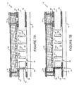
FIGS. 7A and 7B illustrate the cross-sectional view of FIG. 5, in conjunction with the material of the anti-stiction plug “captured” by a trap, in accordance with certain aspects of the present invention;
FIGS. 8A and 8B illustrate cross-sectional views of the fabrication of a microstructure and an anti-stiction plug or cap including a diffusion barrier, according to certain aspects of the present invention;
FIG. 9 illustrates a top view of a portion of another micromechanical structure, for example, a portion of an interdigitated or comb-like finger electrode array, having “moveable” electrodes and “fixed” electrodes, of an accelerometer, in conjunction with, among other things, a plurality of contact areas;
FIGS. 10A-10C and 11A-11C illustrate cross-sectional views (sectioned along dotted line a-a′ of FIG. 1) of the portion of the interdigitated or comb-like finger electrode array, contact area of FIG. 1, in conjunction with the anti-stiction plug or cap, among other things, in accordance with certain aspects of the present invention;
FIG. 12 is a block diagram of microelectromechanical system disposed on a substrate, in conjunction with interface circuitry and data processing electronics;
FIGS. 13A and 13B illustrate cross-sectional views of MEMS according to certain aspects of the present inventions, including a micromachined mechanical structure portion and an integrated circuit portion, both portions of which are disposed or integrated on or in a common substrate;
FIG. 14 illustrates a cross-sectional view (sectioned along dotted line a-a′ of FIG. 1) of the portion of the interdigitated or comb-like finger electrode array and contact area of FIG. 1, in conjunction with the anti-stiction plug or cap and wafer bonded encapsulation structure, in accordance with certain aspects of the present invention;
FIGS. 15A-15F illustrate cross-sectional views of the fabrication of the MEMS, including anti-stiction plug or cap, of FIG. 14 at various stages of the process, according to certain aspects of the present invention;
FIGS. 16A-16F cross-sectional view (sectioned along dotted line a-a′ of FIG. 1) of the portion of the interdigitated or comb-like finger electrode array, contact area and a trench isolated contact, in conjunction with an anti-stiction plug or cap, at various stages of the process, in accordance with another aspect of the present invention;
FIGS. 17A-17E cross-sectional views (sectioned along dotted line a-a′ of FIG. 1) of the portion of the interdigitated or comb-like finger electrode array, contact area and a trench isolated contact, in conjunction with an anti-stiction plug or cap, at various stages of the process, in accordance with another aspect of the present invention;
FIG. 18 illustrates a cross-sectional view of the interdigitated or comb-like finger electrode array, contact area and a trench isolated contact, in conjunction with an anti-stiction plug or cap that is comprised of the same material as the conductive layer disposed above and in contact with the contact area, in accordance with another aspect of the present invention;
FIGS. 19A and 19B illustrate the cross-sectional view of FIG. 18, in conjunction with a trap, in accordance with certain aspects of the present invention;
FIG. 20A is a partial cross-sectional view (sectioned along dotted line a-a′ of FIG. 1) of the portion of the interdigitated or comb-like finger electrode array, in conjunction with a substantially horizontal trap, in accordance with certain aspects of the present invention;
FIG. 20B is a (lateral) cross-sectional view (sectioned along dotted line A-A′) of FIG. 20A illustrating the serpentine shape of the substantially horizontal trap; and
FIGS. 21A and 21B illustrate cross-sectional views of a micromechanical structure, having a plurality of microstructures and a contact, which are monolithically integrated on or within the substrate of a MEMS, in accordance with certain aspect of the present invention.
DETAILED DESCRIPTION
There are many inventions described and illustrated herein. In one aspect, the present invention is directed to a thin film or wafer encapsulated MEMS, and technique of fabricating or manufacturing a thin film or wafer encapsulated MEMS employing the anti-stiction techniques of the present invention. In one embodiment, after encapsulation of the MEMS, an anti-stiction channel is formed in the encapsulation layer(s) and/or the substrate thereby providing “access” to the chamber containing some or all of the active members or electrodes of the mechanical structures of the MEMS. Thereafter, an anti-stiction fluid (for example, gas or gas-vapor) is introduced into the chamber via the anti-stiction channel. The anti-stiction fluid may deposit on one, some or all of the active members or electrodes of the mechanical structures thereby providing an anti-stiction layer (for example, a monolayer coating or self-assembled monolayer) and/or out-gassing molecules on such members or electrodes. In this way, the mechanical structures include suitable anti-stiction characteristics.
After introduction and/or application of the anti-stiction fluid, the anti-stiction channel may be sealed, capped, plugged and/or closed to define and control the mechanical damping environment within the chamber. In this regard, sealing, capping and/or closing the chamber establishes the environment within the chamber containing and/or housing the mechanical structures. This environment provides the predetermined, desired and/or selected mechanical damping of the mechanical structure as well as suitable hermeticity. The parameters (for example, pressure) of the final encapsulated fluid (for example, a gas or a gas vapor) in which the mechanical structures are to operate may be controlled, selected and/or designed to provide a desired and/or predetermined operating environment.
With reference to FIG. 1, in one exemplary embodiment, MEMS 10 includes micromachined mechanical structure 12 that is disposed on substrate 14, for example, an undoped semiconductor-like material, a glass-like material, or an insulator-like material. The micromachined mechanical structure 12 may be an accelerometer, gyroscope and/or other transducer (for example, pressure sensor, strain sensor, tactile sensor, magnetic sensor and/or temperature sensor), filter and/or resonator. The micromachined mechanical structure 12 may also include mechanical structures of a plurality of transducers or sensors including, for example, one or more accelerometers, gyroscopes, pressure sensors, tactile sensors and temperature sensors.
With reference to FIG. 2, in one embodiment, micromachined mechanical structure 12 includes mechanical structures 16 a-d disposed on, above and/or in substrate 14. In particular, mechanical structures 16 a, 16 c and 16 d may be “moveable” electrodes of “moveable” mechanical members 18 a and 18 b. The mechanical structure 16 b may be “fixed” electrodes of “fixed” mechanical member 20. Where micromachined mechanical structure 12 is an accelerometer, mechanical structures 16 a-d may be a portion of the interdigitated or comb-like finger electrode arrays that comprise the sensing features of the accelerometer (see, for example, U.S. Pat. No. 6,122,964).
The mechanical structures 16 a-d may be comprised of, for example, materials in column IV of the periodic table, for example silicon, germanium, carbon; also combinations of these, for example, silicon germanium, or silicon carbide; also of III-V compounds for example, gallium phosphide, aluminum gallium phosphide, or other III-V combinations; also combinations of III, IV, V, or VI materials, for example, silicon nitride, silicon oxide, aluminum carbide, or aluminum oxide; also metallic silicides, germanides, and carbides, for example, nickel silicide, cobalt silicide, tungsten carbide, or platinum germanium silicide; also doped variations including phosphorus, arsenic, antimony, boron, or aluminum doped silicon or germanium, carbon, or combinations like silicon germanium; also these materials with various crystal structures, including single crystalline, polycrystalline, nanocrystalline, or amorphous; also with combinations of crystal structures, for instance with regions of single crystalline and polycrystalline structure (whether doped or undoped).
With continued reference to FIG. 2, micromachined mechanical structure 12 may also include a field area 22 and contact area 24 disposed on or in substrate 14. The field region 22 may provide a substrate material for the electronic or electrical components or integrated circuits (for example, transistors, resistors, capacitors, inductors and other passive or active elements). The contact area 24 may provide an electrical path between micromachined mechanical structure 12 and integrated or external electronics, integrated interface circuitry, and/or an external device (not illustrated). The contact area 24 may be comprised of, for example, silicon, (whether doped or undoped), germanium, silicon/germanium, silicon carbide, and gallium arsenide, and combinations and/or permutations thereof.
The micromachined mechanical structure 12 further includes chamber 26 having an atmosphere 28 “contained” therein. The chamber 26 is formed, at least in part, by encapsulation layer(s) 30. In this regard, MEMS 10 may be sealed in chamber 26 using conventional thin film encapsulation techniques and structures. (See, for example, WO 01/77008 A1 and WO 01/77009 A1). Other thin film encapsulation techniques are suitable. Indeed, all thin film encapsulation techniques, whether now known or later developed, are intended to be within the scope of the present invention.
For example, the encapsulation techniques described and illustrated in non-provisional Patent Application entitled “Microelectromechanical Systems Having Trench Isolated Contacts, and Methods of Fabricating Same”, which was filed on Jun. 4, 2003 and assigned Ser. No. 10/455,555 (hereinafter “Microelectromechanical Systems Having Trench Isolated Contacts Patent Application”), may be employed in conjunction with the anti-stiction techniques of the present invention. For the sake of brevity, the inventions described and illustrated in the Microelectromechanical Systems Having Trench Isolated Contacts Patent Application, implemented in conjunction with the inventions described and illustrated herein, will not be repeated but will only be summarized. It is expressly noted, however, that the entire contents of the Microelectromechanical Systems Having Trench Isolated Contacts Patent Application, including, for example, the features, attributes, alternatives, materials, techniques and advantages of all of the inventions, are incorporated by reference herein.
The micromachined mechanical structure 12 of the present invention also includes anti-stiction channel 32 formed through, for example, encapsulation layer(s) 30 to facilitate fluid communications with and/or provide an access or a pathway to mechanical structures 16 a-d in chamber 26 after completion of the encapsulation process (i.e., deposition, formation and/or growth of encapsulation layer(s) 30). In this regard, after encapsulation of mechanical structures 16 a-d and formation of chamber 26, anti-stiction channel 32 may be formed using, for example, anisotropic etching techniques (for example, deep reactive ion etching). In one embodiment, “diameter” or “width” of anti-stiction channel 32 may be between 100 nm to 50 μm and preferably between 200 nm and 10 μm. Notably, the “diameter” or “width” of anti-stiction channel 32 may depend on the thickness of the encapsulation layer(s) 30.
Thereafter, an anti-stiction fluid (for example, dichlordimethylsilan (“DDMS”), octadecyltrichlorsilan (“OTS”), perfluoroctyltrichlorsilan (“PFOTCS”), perfluorodecanoic acid (“PFDA”), perfluorodecyl-trichlorosilane (“FDTS”), perfluoro polyether (“PFPE”) and/or fluoroalkylsilane (“FOTS”)) may be introduced into chamber 26 by, for example, vapor deposition (for example, APCVD, LPCVD, or PECVD). The anti-stiction fluid may deposit on one, some or all of mechanical structures 16 a-d of MEMS 12 thereby providing an anti-stiction layer, for example, a monolayer coating and/or out-gassing molecules on the mechanical structures. In this way, mechanical structures 16 a-d include suitable anti-adhesive properties.
The parameters of introducing the anti-stiction fluid may impact, for example, the characteristics of the anti-stiction layer (for example, the monolayer or self-assembled monolayer) on mechanical structures 16 a-d. For example, introducing the anti-stiction fluid at higher temperatures may tend to enhance the diffusivity of the fluid whereas introducing the anti-stiction fluid at lower temperatures may tend to enhance the anti-stiction properties of the fluid. Thus, in one embodiment, the anti-stiction fluid is introduced between 20° C. to 600° C., and preferably between 100° C. and 300° C.
Moreover, introducing the anti-stiction fluid at higher pressures may tend to enhance the deposition rate of the anti-stiction layer (for example, the monolayer or self-assembled monolayer) on mechanical structures 16 a-d. In contrast, lower pressures may increase the number of molecules that enter further down into chamber 26 due to the larger mean free path of the molecules via anti-stiction channel 32. Thus, in one embodiment, the anti-stiction fluid is introduced between 100 μTorr and 1 Torr.
It may be advantageous to employ deposition parameters of the anti-stiction layer that provides or forms the anti-stiction layer more conformally. In this way, anti-stiction channel 32 is less likely to close, as a result of “build-up” of the anti-stiction material within or above anti-stiction channel 32, before a sufficient anti-stiction layer forms on mechanical structures 16 a-d. Notably, the anti-stiction fluid may be any material that enhances the non-reactive and/or non-adhesive nature of, for example, the surface of mechanical structures 16 a-d.
The anti-stiction channel 32 may be “closed” and/or “sealed” via channel plug 34. In this regard, channel plug 34 may be any material that seals, plugs and/or closes anti-stiction channel 32. For example, channel plug 34 may be a spin-on polymer, spin-on glass (“SOG”), metal material (for example, metal that is sputtered and, if necessary patterned). Further, channel plug 34 may be formed using/from silk screening of or dispensed seal-glass, plastic and/or epoxy. In addition, a shadow mask technology may be employed to seal, plug and/or close anti-stiction channel 32. Indeed, any material (and corresponding fabrication technique) may be implemented that, in one embodiment, provides a barrier to maintain a suitable environment in chamber 26 and is formed, applied and/or grown using parameters (for example, a temperature) that will not (1) destroy and/or obliterate the anti-stiction affects provided by the anti-stiction fluid (for example, destruction of the monolayer coating on the mechanical structures) and/or (2) prevent the anti-stiction technique of the present invention from providing suitable anti-stiction characteristics. In this way, after sealing and/or closing anti-stiction channel 32, mechanical structures 16 a-d retain suitable anti-stiction characteristics and/or properties.
As mentioned above, an exemplary method of fabricating or manufacturing a thin film encapsulated MEMS 10 is described and illustrated in the Microelectromechanical Systems Having Trench Isolated Contacts Patent Application. For the sake of brevity, those discussions and illustrations will not be repeated but will only be summarized. It is expressly noted, however, that the entire contents of the Microelectromechanical Systems Having Trench Isolated Contacts Patent Application, including, for example, the features, attributes, alternatives, materials, techniques and advantages of all of the inventions, are incorporated by reference herein.
With reference to FIG. 3A, MEMS 10 may begin with an SOI substrate partially formed device including mechanical structures 16 a-d and contact area 24 disposed on first sacrificial layer 36, for example, silicon dioxide or silicon nitride. The mechanical structures 16 a-d and contact area 24 may be formed using well-known deposition, lithographic, etching and/or doping techniques as well as from well-known materials (for example, semiconductors such as silicon, germanium, silicon-germanium or gallium-arsenide). Moreover, field region 22 and first sacrificial layer 36 may be formed using well-known silicon-on-insulator fabrication techniques (FIG. 3A) or well-known formation, lithographic, etching and/or deposition techniques using a standard or over-sized (“thick”) wafer (not illustrated).
With reference to FIG. 3B, following formation of mechanical structures 16 a-d and contact area 24, second sacrificial layer 38, for example, silicon dioxide or silicon nitride, may be deposited and/or formed to secure, space and/or protect mechanical structures 16 a-d during subsequent processing, including the encapsulation process. In addition, an opening 40 may be etched and/or formed in second sacrificial layer 38 to provide for subsequent formation of an electrical contact. The opening 40 may be provided using, for example, well known masking techniques (such as a nitride mask) prior to and during deposition and/or formation of second sacrificial layer 38, and/or well known lithographic and etching techniques after deposition and/or formation of second sacrificial layer 38.
With reference to FIGS. 3C, 3D and 3E, thereafter, first encapsulation layer 30 a may be deposited, formed and/or grown on second sacrificial layer 38 (see, FIG. 3C). In one embodiment, the thickness of first encapsulation layer 30 a in the region overlying second sacrificial layer 38 may be between 0.1 μm and 5.0 μm. The external environmental stress on, and internal stress of first encapsulation layer 30 a after etching second sacrificial layer 38 may impact the thickness of first encapsulation layer 30 a. Slightly tensile films may self-support better than compressive films which may buckle.
The first encapsulation layer 30 a may be etched to form passages or vents 42 (see, FIG. 3D). In one exemplary embodiment, vents 42 have a diameter or aperture size of between 0.1 μm to 2 μm. The vents 42 permit etching and/or removal of at least selected portions of first and second sacrificial layers 36 and 38, respectively (see, FIG. 3E).
As mentioned in the Microelectromechanical Systems Having Trench Isolated Contacts Patent Application, contact 24 may remain partially, substantially or entirely surrounded by portions of first and second sacrificial layers 36 and/or 38. For example, with reference to FIG. 3E, while mechanical structures 16 a-16 d are released from their respective underlying oxide columns, a portion 44 of sacrificial layer 38 (i.e., juxtaposed electrical contact area 24 may remain after etching or removing second sacrificial layer 38.
With reference to FIG. 3F, after releasing mechanical elements 16 a-d, second encapsulation layer 30 b may be deposited, formed and/or grown. The second encapsulation layer 30 b may be, for example, a silicon-based material (for example, a polycrystalline silicon or silicon-germanium), which is deposited using, for example, an epitaxial, a sputtering or a CVD-based reactor (for example, APCVD, LPCVD, or PECVD). The deposition, formation and/or growth may be by a conformal process or non-conformal process. The material may be the same as or different from first encapsulation layer 30 a.
Thereafter, contact area 24 of micromachined mechanical structure 12 is dielectrically isolated from the surrounding conductor and/or semiconductor layers. With reference to FIGS. 3G and 3H, trenches 46 a and 46 b may be etched. The trenches 46 a and 46 b may include a slight taper in order to facilitate the formation of dielectric isolation regions 48 a and 48 b. In this regard, an insulating material may be deposited in trenches 46 a and 46 b to form dielectric isolation regions 48 a and 48 b, respectively. The insulating material may be, for example, silicon dioxide, silicon nitride, BPSG, PSG, or SOG.
The insulating layer 50 may be deposited, formed and/or grown on the exposed surface of second encapsulating layer 30 b to provide insulation between the various surrounding conductive and/or semiconductor layers and the subsequent conductive layer. Thus, during deposition, formation and/or growth of insulation layer 50, trenches may also be filled to form dielectric isolation regions 48 a and 48 b. (see, FIG. 3H). Thereafter, contact opening 52 may be etched to facilitate electrical connection to contact area 24. A conductive layer 54 may then be deposited and/or formed to provide the appropriate electrical connection to contact 24. (see, FIG. 31).
Thereafter, with reference to FIG. 3J, anti-stiction channel window 56 may be formed and/or etched in insulation layer 50, using conventional etching techniques, in order to define the location of anti-stiction channel 32 (see, FIG. 3K). The anti-stiction channel 32 is formed through encapsulation layer(s) 30 to provide access to mechanical structures 16 a-d. The anti-stiction channel 32 may be formed using, for example, well-known anisotropic etching techniques (for example, deep reactive ion etching).
After formation of anti-stiction channel 32, an anti-stiction fluid may be introduced into chamber 26. The anti-stiction fluid may be, for example, DDMS, OTS, PFOTCS, PFDA, FDTS, PFPE and/or FOTS. Indeed, any anti-stiction fluid may be employed provided that the subsequent processes do not destroy the anti-stiction characteristics and/or destroy or obliterate the anti-stiction deposition on mechanical structures 16 a-d of MEMS 12. In this way, anti-stiction layer 58 (exemplary illustration in FIG. 4), for example, the monolayer coating formed on mechanical structures 16 a-d, remains relatively intact and mechanical structures 16 a-d include suitable anti-adhesive properties to overcome the adhesive forces of adjacent structures or elements in MEMS 10.
With reference to FIG. 3L, anti-stiction channel 32 may be closed via channel plug 34. In this regard, channel plug 34 may be any material that seals, plugs and/or closes anti-stiction channel 32. For example, channel plug 34 may be a spin-on polymer, spin-on glass (“SOG”), metal material that is sputtered and, if necessary patterned. Further, channel plug 34 may be formed using/from silk screening of seal-glass, plastic and/or epoxy. In addition, a shadow mask technology may be employed to seal, plug and/or close anti-stiction channel 32. Indeed, any material (and corresponding fabrication technique) may be employed to form channel plug 34 provided the process of forming channel plug 34 uses parameters (for example, a temperature) that will not (1) destroy and/or obliterate the anti-stiction affects provided by the anti-stiction fluid (for example, destruction of the monolayer coating on the mechanical structures) and/or (2) prevent the anti-stiction technique of the present invention from providing suitable anti-stiction or anti-adhesive characteristics.
Notably, the anti-stiction fluid may be a gas or gas vapor of a material used during the formation of channel plug 34. Indeed, the anti-stiction fluid may be a by-product of the reaction of the material of MEMS 10 and the gas or gas vapor of a material used during the formation of channel plug 34. For example, a mixture of solvents and/or a polymer which outgases appropriate molecules such as DDMS.
The state of the fluid within chamber 26 (for example, the pressure), after deposition and/or formation of channel plug 34 may be determined using conventional techniques and/or using those techniques described and illustrated in non-provisional patent application entitled “Electromechanical System having a Controlled Atmosphere, and Method of Fabricating Same”, which was filed on Mar. 20, 2003 and assigned Ser. No. 10/392,528 (hereinafter “the Electromechanical System having a Controlled Atmosphere Patent Application”). For the sake of brevity, all of the inventions regarding controlling the atmosphere within chamber 26 which are described and illustrated in the Electromechanical System having a Controlled Atmosphere Patent Application will not be repeated here. It is expressly noted, however, that the entire contents of the Electromechanical System having a Controlled Atmosphere Patent Application, including, for example, the features, attributes, alternatives, materials, techniques and advantages of all of the inventions, are incorporated by reference herein.
With reference to FIG. 4, in certain embodiments, anti-stiction layer 58, for example, a thin and/or monolayer coating is formed on mechanical structures 16 a-d as a result of the introduction of the anti-stiction fluid and/or formation of channel plug 34. The thin and/or monolayer coating provides suitable anti-adhesive properties that overcome the adhesive forces of adjacent structures or elements in MEMS 10. Notably, anti-stiction layer 58, for example, the thin and/or monolayer coating does not detrimentally impact the operation of mechanical structures 12 of MEMS 10.
In another embodiment of the present invention, a vertical and/or horizontal trap is formed in the vicinity of anti-stiction channel 32. The trap 60 may be positioned between anti-stiction channel 32 and mechanical structures 16 a-d (see, for example. FIG. 5). In this way, where certain materials (i.e., the material(s) used to form channel plug 34) are employed to seal, plug and/or close anti-stiction channel 32 that may escape from anti-stiction channel 32, trap 60 “captures” or “catches” that material before it enters that portion of chamber 26 where mechanical structures 16 a-d reside. Under this circumstance, the channel plug material that enters chamber 26 is routed away from mechanical structures 16 a-d and, as such, is “prevented” from contacting and/or impacting mechanical structures 16 a-d and the operation thereof. For example, with reference to FIG. 5, trap 60 may be a substantially vertical trap, which is located between anti-stiction channel 32 and mechanical structures 16 a-d.
With reference to FIG. 6A, an exemplary embodiment of MEMS 10 having trap 60 may begin with an SOI substrate partially formed device including mechanical structures 16 a-d, contact area 24, and trap 60 disposed on first sacrificial layer 36, for example, silicon dioxide or silicon nitride. The mechanical structures 16 a-d, contact area 24 and trap 60 may be formed using well-known deposition, lithographic, etching and/or doping techniques as well as from well-known materials (for example, semiconductors such as silicon, germanium, silicon-germanium or gallium-arsenide).
Thereafter, the processing of MEMS 10 having trap 60 may proceed in the same manner as described above with respect to FIGS. 3B-3L. In this regard, an exemplary fabrication process of MEM 10 including trap 60 is illustrated in FIGS. 6B-6L. Because the processes are substantially similar to the discussion above with respect to FIGS. 3B-3L, for the sake of brevity, that discussion will not be repeated.
As mentioned above, trap 60 of FIG. 5 is designed to prevent the material(s) that are deposited to seal, plug and/or close anti-stiction channel 32 from adversely impacting the operation of mechanical structures 16 a-d. With reference to FIGS. 7A and 7B, in one embodiment, trap 60 is positioned and/or located to route material 62 that may leak and/or escape from anti-stiction channel 32 during deposition and/or formation of channel plug 34 away from mechanical structures 16 a-d. In this regard, trap 60 “captures” material 62 before it enters that portion of chamber 26 where mechanical structures 16 a-d reside. Under this circumstance, material 62 that enters chamber 26 is “prevented” from contacting and/or adversely impacting mechanical structures 16 a-d and the operation thereof.
With reference to FIGS. 8A and 8B, in another embodiment, after fabrication of channel plug 34, diffusion barrier 64 may be deposited and/or formed over anti-stiction channel 32 and/or channel plug 34 in order to enhance the “seal” of anti-stiction channel 32 and thereby enhance the barrier to diffusion of fluid within (or external to) chamber 26 (for example, enhance the hermeticity of MEMS 10). Thus, diffusion barrier 64 alone, or in combination with channel plug 34, “traps” the fluid (having a selected, desired and/or predetermined state) in chamber 26.
The diffusion barrier 64 may be, for example, a semiconductor material (for example, a polysilicon, germanium, or silicon/germanium), an insulator material (for example, silicon dioxide, silicon nitride, BPSG, PSG, or SOG) or metal bearing material (for example, silicides). The diffusion barrier 64 may be, for example deposited, formed or grown using, for example, an epitaxial, a sputtering or a CVD-based reactor (for example, APCVD, LPCVD or PECVD). The deposition, formation and/or growth may be by a conformal process or non-conformal process. The material comprising diffusion barrier 64 may be the same as or different from channel plug 34. However, it may be advantageous to employ a low temperature deposition process (and a material that is amenable to such a deposition technique) in order to preserve and/or protect the anti-stiction barrier, layer and/or affects provided by the anti-stiction fabrication processes of the present invention.
The diffusion barrier 64 may be formed and/or deposited before formation and/or deposition of conductive layer 54, during formation and/or deposition of conductive layer 54 (see, for example, FIG. 8A), or after formation and/or deposition of conductive layer 54 (see, for example, FIG. 8B).
Notably, diffusion barrier 64 may be implemented in any of the embodiments described herein, for example, the embodiments illustrated in FIGS. 3A-3L. For the sake of brevity, that discussion will not be repeated or restated.
As mentioned above, the present inventions may be implemented in conjunction with various thin film encapsulation techniques, including the encapsulation techniques described and illustrated in non-provisional Patent Application entitled “Microelectromechanical Systems, and Method of Encapsulating and Fabricating Same”, which was filed on Jun. 4, 2003 and assigned Ser. No. 10/454,867 (hereinafter “Microelectromechanical Systems and Method of Encapsulating Patent Application”). In this regard, any and all of the embodiments described herein may be incorporated into the MEMS 10 of Microelectromechanical Systems and Method of Encapsulating patent application (see, for example FIGS. 9, 10A-10C, and 11A-11C). For the sake of brevity, the inventions described and illustrated in the Microelectromechanical Systems and Method of Encapsulating Patent Application, implemented in conjunction with the anti-stiction inventions described and illustrated herein, will not be repeated. It is expressly noted, however, that the entire contents of the Microelectromechanical Systems and Method of Encapsulating Patent Application, including, for example, the features, attributes, alternatives, materials, techniques and advantages of all of the embodiments and/or inventions, are incorporated by reference herein.
It should be noted that the present invention may be implemented in a MEMS including micromachined mechanical structure as well as data processing electronics and/or interface circuitry. With reference to FIG. 12, in one exemplary embodiment, MEMS 10 includes micromachined mechanical structure 12 that is disposed on substrate 14, for example, an undoped semiconductor-like material, a glass-like material, or an insulator-like material. The MEMS 10 may also include data processing electronics 70 to process and analyze information generated by, and/or control or monitor the operation of micromachined mechanical structure 12. In addition, MEMS 10 may also include interface circuitry 72 to provide information from micromachined mechanical structure 12 and/or data processing electronics 70 to an external device (not illustrated), for example, a computer, indicator/display and/or sensor.
The data processing electronics 70 and/or interface circuitry 72 may be integrated in or on substrate 14. In this regard, MEMS 10 may be a monolithic structure including mechanical structure 12, data processing electronics 70 and interface circuitry 72. The data processing electronics 70 and/or interface circuitry 72 may also reside on a separate, discrete substrate that, after fabrication, is bonded to or on substrate 14.
For example, with reference to FIGS. 13A and 13B, integrated circuits 74 may be fabricated using conventional techniques after definition of mechanical structure 12 using, for example, the techniques described and illustrated in Microelectromechanical Systems and Method of Encapsulating Patent Application and/or Microelectromechanical Systems Having Trench Isolated Contacts Patent Application (see, for example, FIG. 13B). In this regard, after fabrication and encapsulation of mechanical structure 12, integrated circuits 74 may be fabricated using conventional techniques and interconnected to contact area 24 by way of conductive layer 54. In particular, as illustrated and described in Microelectromechanical Systems and Method of Encapsulating Patent Application (for example, FIGS. 12A-C thereof and/or Microelectromechanical Systems Having Trench Isolated Contacts Patent Application (for example, FIGS. 14A-E thereof, the contact area is accessed directly by integrated circuitry 74 via a low resistance electrical path (i.e., conductive layer 54) that facilitates a good electrical connection. The insulation layer 50 may be deposited, formed and/or grown and patterned and, thereafter, conductive layer 54 (for example, a heavily doped polysilicon or metal such as aluminum, chromium, gold, silver, molybdenum, platinum, palladium, tungsten, titanium, and/or copper) is formed.
With continued reference to FIGS. 13A and 13B, thereafter, the anti-stiction techniques of the present invention(s) may be implemented. That is, the anti-stiction channel window may be etched and/or formed in insulation layer 50 and anti-stiction channel 32 may be etched and/or formed in encapsulation layer(s) 30. The anti-stiction fluid may be introduced into chamber 26 via anti-stiction channel 32 thereby forming, for example, an anti-stiction layer on mechanical structures 16. Thereafter or concurrently therewith, anti-stiction channel 32 may be closed and/or sealed by channel plug 34 and/or diffusion barrier 64.
Notably, while the anti-stiction processes were described as being implemented after deposition and/or formation of insulation layer 50 and conductive layer 54, the anti-stiction processes of the MEMS 10 illustrated in FIGS. 13A and 13B may be performed in another order. That is, contact opening 52 and anti-stiction channel window 56 may be fabricated either consecutively or simultaneously. Moreover, the anti-stiction fabrication/processes may be performed after deposition of conductive layer 54 or before fabrication of deposition of conductive layer 54. In addition, channel plug 34 may be formed and/or deposited simultaneously with the formation and/or deposition of conductive layer 54.
In another aspect, the present invention employs wafer-bonding encapsulation techniques, in conjunction with the anti-stiction techniques described above. In this regard, with reference to FIG. 14, in one embodiment, MEMS 10 includes micromachined mechanical structure 12 and wafer bonded encapsulation structure 76. The micromachined mechanical structure 12 may be fabricated using any of the techniques described and illustrated herein or using conventional techniques.
The wafer bonded encapsulation structure 76 may be bonded and/or “attached”, using, for example, anodic bonding. In one embodiment, wafer bonded encapsulation structure 76 includes cap wafer 78 (for example, silicon), insulation layer 80 (for example, SOG or Pyrex) and anodic shield 82 (for example, a metal). Notably, wafer bonded encapsulation structure 76 may be bonded and/or “attached” using conventional techniques.
In one embodiment, the anti-stiction techniques described and illustrated above are “applied” to the exposed surface of substrate 14. In this regard, anti-stiction channel 32 is formed in substrate 14 and, thereafter an anti-stiction fluid is introduced into chamber 26, as described above. The anti-stiction plug 34 is then deposited and/or formed to “re-seal” chamber 26.
For example, with reference to FIG. 15A, MEMS 10 may begin with an SOI substrate partially formed device including “released” mechanical structures 16 a-d and contact area 24 partially disposed on first sacrificial layer 36, for example, silicon dioxide or silicon nitride. The fabrication and/or formation of the structures of micromachined mechanical structure 12 may be accomplished using the techniques described and illustrated herein or any conventional technique. Indeed, all techniques and materials used to fabricate and/or form mechanical structure 12, whether now known or later developed, are intended to be within the scope of the present invention.
With reference to FIG. 15B, thereafter, wafer bonded encapsulation structure 76 may be “applied” and/or bonded to micromachined mechanical structure 12. For example, in one embodiment, wafer bonded encapsulation structure 76 is bonded using anodic techniques. Notably, wafer bonded encapsulation structure 76 may be “bonded” to micromachined mechanical structure 12 using conventional techniques. In addition, all techniques and materials used to fabricate and/or form wafer bonded encapsulation structure 76, whether now known or later developed, are intended to be within the scope of the present invention.
With reference to FIGS. 15C and 15D, substrate 14 may be thinned (for example, to a thickness of between 20 μm to 200 μm, to facilitate contact or interconnection to contact area 24. In this regard, contact area 24 may be isolated via trenches 46 a and 46 b using an anisotropic etching technique (see, FIG. 15C) as described in detail above. Thereafter, an electrical path may be deposited and/or formed to interconnect contact area 24 with, for example, integrated or external electronics and/or circuitry. In this regard, conductive layer 54 may be deposited and/or formed after deposition of insulation layer 50. (See, FIG. 15D)
With reference to FIGS. 15E and 15F, anti-stiction channel 32 may be formed (see, FIG. 15E), and an anti-stiction fluid may be introduced into chamber 26. The techniques described and illustrated above may be applied here. After (or concurrently with) introduction of the anti-stiction fluid, channel plug 34 may be deposited and/or formed to “seal” anti-stiction channel 32. As mentioned above, channel plug 34 may be a spin-on polymer, SOG, metal material. Moreover, channel plug 34 may be formed using/from silk screening of or dispensed seal-glass, plastic and/or epoxy. Indeed, any material (and corresponding fabrication technique) may be implemented that, in one embodiment, provides a barrier to maintain a suitable environment in chamber 26 and is formed, applied and/or grown using parameters (for example, a temperature) that will not (1) destroy and/or obliterate the anti-stiction affects provided by the anti-stiction fluid (for example, destruction of the monolayer coating on the mechanical structures) and/or (2) prevent the anti-stiction technique of the present invention from providing suitable anti-stiction characteristics.
Notably, as described above, a diffusion barrier may be incorporated to enhance the “seal” of chamber 26. The diffusion barrier alone, or in combination with channel plug 34, “traps” the fluid (having a selected, desired and/or predetermined state) in chamber 26. Thus, after sealing and/or closing anti-stiction channel 32, mechanical structures 16 a-d retain suitable anti-stiction characteristics and/or properties.
It should be further noted that all of the anti-stiction techniques described and illustrated in connection with the thin film wafer fabrication (for example, FIGS. 2, 5, 8A and 8B) may be applied to the wafer bonded encapsulation embodiment. For the sake of brevity, those discussions will not be repeated.
There are many inventions described and illustrated herein. While certain embodiments, features, materials, configurations, attributes and advantages of the inventions have been described and illustrated, it should be understood that many other, as well as different and/or similar embodiments, features, materials, configurations, attributes, structures and advantages of the present inventions that are apparent from the description, illustration and claims. As such, the embodiments, features, materials, configurations, attributes, structures and advantages of the inventions described and illustrated herein are not exhaustive and it should be understood that such other, similar, as well as different, embodiments, features, materials, configurations, attributes, structures and advantages of the present inventions are within the scope of the present invention.
For example, while the exemplary embodiments and/or processes of the invention have been described above according to a particular order, that order should not be interpreted as limiting. For example, contact opening 52 and anti-stiction channel window 56 may be fabricated either consecutively (see, for example, FIGS. 3I-3K and FIGS. 16B-16E) or simultaneously (see, for example, FIG. 20B). Moreover, the anti-stiction fabrication/processes may be performed after deposition of conductive layer 54 (see, for example, FIGS. 3J-3L) or before fabrication of deposition of conductive layer 54 (see, for example, FIGS. 17A-17F).
Indeed, anti-stiction channel 32 may be comprised of a plurality of channels etched in substrate 14, encapsulation layer(s) 30 and/or wafer bonded encapsulation structure 76. The channels may be located at selected sites to more efficiently, fully and/or evenly provide the anti-stiction fluid within chamber and thereby more efficiently, fully and/or evenly/conformally provide an anti-stiction layer (for example, a monolayer coating or self-assembled monolayer) on micromachined mechanical structure 12. In this regard, the anti-stiction channels 32 may be, for example, evenly situated or placed around substrate 14, encapsulation layer(s) 30 and/or wafer bonded encapsulation structure 76, or distributed according to the relative concentration of structures 16 (for example, more channels 32 concentrated in regions or areas of dense mechanical structures and/or less channels 32 concentrated in regions or areas of less “populated” by mechanical structures).
In addition, it may be advantageous to locate the anti-stiction channels 32 in accordance with regions or areas where the mechanical structures are more likely to contact other structures or elements of micromachined mechanical structure 12 and/or are more susceptible to the debilitating effects of stiction. In this way, the anti-stiction fluid is more likely to efficiently, fully and/or evenly/conformally provide an anti-stiction layer (for example, a monolayer coating or self-assembled monolayer) on such mechanical structures of micromachined mechanical structure 12.
Further, channel plug 34 may be formed and/or deposited simultaneously with the formation and/or deposition of conductive layer 54. In this embodiment, channel plug 34 may be a metal or highly doped semiconductor material (for example, highly doped polysilicon). (See, for example, FIG. 18). In those instances where channel plug 34 is comprised of a metal, it may be advantageous to employ trap 60 to “protect” micromachined mechanical structure 12 in the event that the metal material enters chamber 26 (see, for example, FIGS. 19A and 19B).
Moreover, trap 60 may take any vertical and/or horizontal shape in one or more of the layers of micromachined mechanical structure 12. For example, trap 60 may be formed within encapsulation layer(s) 30 as a substantially horizontal trap that includes serpentine shape before access to chamber 26 (see, for example, FIGS. 20A and 20B).
In addition, as mentioned above, the anti-stiction techniques described herein may be implemented in conjunction with micromachined mechanical structures 12 having one or more transducers or sensors which may themselves include multiple layers that are vertically and/or laterally stacked or interconnected as illustrated in Microelectromechanical Systems and Method of Encapsulating Patent Application and/or Microelectromechanical Systems Having Trench Isolated Contacts Patent Application. Accordingly, any and all of the anti-stiction inventions and/or embodiments illustrated and described herein may be implemented in the embodiments of Microelectromechanical Systems and Method of Encapsulating Patent Application and/or Microelectromechanical Systems Having Trench Isolated Contacts Patent Application that include multiple layers of mechanical structures, contacts areas and buried contacts that are vertically and/or laterally stacked or interconnected (see, for example, micromachined mechanical structure 12 of FIGS. 11B, 11C and 11D of Microelectromechanical Systems and Method of Encapsulating Patent Application and/or micromachined mechanical structure 12 of FIGS. 13B, 13C and 13D of Microelectromechanical Systems Having Trench Isolated Contacts patent application). Under this circumstance, the MEMS may be fabricated using the anti-stiction techniques described in this application wherein the mechanical structures include one or more processing steps to provide the vertically and/or laterally stacked and/or interconnected multiple layers (see, for example, FIGS. 21A and 21B).
Thus, any of the techniques, materials and/or embodiments of fabricating and/or encapsulating micromachined mechanical structure 12 that are described in the Microelectromechanical Systems and Method of Encapsulating Patent Application and/or in the Microelectromechanical Systems Having Trench Isolated Contacts Patent Application may be employed with the embodiments and/or the inventions described herein.
Moreover, the present invention may implement the anchors and techniques of anchoring mechanical structures 16 to substrate 14 (as well as other elements of MEMS 10, for example, contact 24) described and illustrated in “Anchors for Microelectromechanical Systems Having an SOI Substrate, and Method for Fabricating Same”, which was filed on Jul. 25, 2003 and assigned Ser. No. 10/627,237 (hereinafter the “Anchors for Microelectromechanical Systems Patent Application”). In this regard, with reference to FIGS. 19A and 19B, in one embodiment, anchors 66 and/or 68 may be comprised of a material that is relatively unaffected by the release processes of the mechanical structures. In this regard, the etch release process are selective or preferential to the material(s) securing mechanical structures 16 in relation to the material comprising anchors 66. Moreover, anchors 66 and/or 68 may be secured to substrate 14 in such a manner that removal of insulation layer 50 has little to no affect on the anchoring of mechanical structures 16 to substrate 14.
It should be noted that the embodiments described herein may be incorporated into MEMS 10 described and illustrated in Anchors for Microelectromechanical Systems patent application. For the sake of brevity, the inventions and/or embodiments described and illustrated in the Anchors for Microelectromechanical Systems Patent Application, implemented in conjunction with the anti-stiction inventions described and illustrated herein, will not be repeated. It is expressly noted, however, that the entire contents of the Anchors for Microelectromechanical Systems Patent Application, including, for example, the features, attributes, alternatives, materials, techniques and advantages of all of the embodiments and/or inventions, are incorporated by reference herein.
The term “depositing” and other forms (i.e., deposit, deposition and deposited) in the claims, means, among other things, depositing, creating, forming and/or growing a layer of material using, for example, a reactor (for example, an epitaxial, a sputtering or a CVD-based reactor (for example, APCVD, LPCVD, or PECVD)).
Further, in the claims, the term “contact” means a conductive region, partially or wholly disposed outside the chamber, for example, the contact area and/or contact via.
It should be further noted that while the present inventions have been described in the context of microelectromechanical systems including micromechanical structures or elements, the present inventions are not limited in this regard. Rather, the inventions described herein are applicable to other electromechanical systems including, for example, nanoelectromechanical systems. Thus, the present inventions are pertinent to electromechanical systems, for example, gyroscopes, resonators, temperatures sensors and/or accelerometers, made in accordance with fabrication techniques, such as lithographic and other precision fabrication techniques, which reduce mechanical components to a scale that is generally comparable to microelectronics. Indeed, any MEMS structure that is encapsulated by using thin film packaging or wafer bonding techniques, and subsequently “opened”, and, after application or introduction of an anti-stiction fluid, is “re-sealed” is to be within the scope of the present invention.
Finally, as mentioned above, all of the embodiments of the present invention described and illustrated herein may be implemented in the embodiments of Microelectromechanical Systems and Method of Encapsulating Patent Application and/or Microelectromechanical Systems Having Trench Isolated Contacts Patent Application and/or Anchors for Microelectromechanical Systems Patent Application. For the sake of brevity, those permutations and combinations will not be repeated but are incorporated by reference herein.

Claims (28)

1. An electromechanical device comprising:
a substrate;
a mechanical structure disposed over the substrate wherein a monolayer or self-assembled layer is disposed on at least a portion of the mechanical structure;
a film encapsulation structure, disposed over the mechanical structure, to seal a chamber;
an anti-stiction channel, etched into the film encapsulation structure, to provide access to at least a portion of the mechanical structure disposed in the chamber; and
an anti-stiction plug, disposed over or in the anti-stiction channel, to re-seal the chamber.
2. The device of claim 1 wherein the film encapsulation structure includes first and second encapsulation layers.
3. The device of claim 2 wherein the first encapsulation layer includes polycrystalline silicon, porous polycrystalline silicon, amorphous silicon, silicon carbide, silicon nitride, silicon/germanium, germanium, or gallium arsenide.
4. The device of claim 2 wherein the second encapsulation layer includes polycrystalline silicon, porous polycrystalline silicon, amorphous silicon, germanium, silicon/geranium, gallium arsenide, or silicon carbide.
5. The device of claim 1 wherein the anti-stiction plug includes spin-on polymer, SOG or a metal material.
6. The device of claim 1 wherein the anti-stiction plug includes spin-on polymer or SOG which is deposited using silk screening.
7. The device of claim 1 wherein the anti-stiction plug includes spin-on polymer or SOG which is deposited using dispensed seal-glass, plastic and/or epoxy.
8. The device of claim 1 wherein the anti-stiction plug is deposited using a shadow mask technology.
9. The device of claim 1 further including a trap, disposed between the anti-stiction channel and the mechanical structure.
10. The device of claim 9 wherein the trap is a substantially vertical trap.
11. The device of claim 9 wherein the trap is a substantially horizontal trap.
12. The device of claim 1 further including a diffusion barrier disposed over the anti-stiction plug.
13. The device of claim 12 wherein the diffusion barrier includes a metal material.
14. An electromechanical device comprising:
a substrate;
a mechanical structure disposed over the substrate wherein an anti-stiction layer is disposed on at least a portion of the mechanical structure;
a film encapsulation structure, disposed over the mechanical structure, to define, in part, a chamber;
an anti-stiction channel, formed in the film encapsulation structure, to allow the anti-stiction layer to be disposed on at least the portion of the mechanical structure disposed in the chamber; and
an anti-stiction plug, disposed over or in the anti-stiction channel, to re-seal the chamber.
15. The device of claim 14 wherein the film encapsulation structure includes first and second encapsulation layers.
16. The device of claim 15 wherein the first encapsulation layer includes polycrystalline silicon, porous polycrystalline silicon, amorphous silicon, silicon carbide, silicon nitride, silicon/germanium, germanium, or gallium arsenide.
17. The device of claim 15 wherein the second encapsulation layer includes polycrystalline silicon, porous polycrystalline silicon, amorphous silicon, germanium, silicon/germanium, gallium arsenide, or silicon carbide.
18. The device of claim 14 wherein the anti-stiction plug includes spin-on polymer, SOG or a metal material.
19. The device of claim 14 wherein the anti-stiction plug includes spin-on polymer or SOG which is deposited using silk screening.
20. The device of claim 14 wherein the anti-stiction plug includes spin-on polymer or SOG which is deposited using dispensed seal-glass, plastic and/or epoxy.
21. The device of claim 14 wherein the anti-stiction plug is deposited using a shadow mask technology.
22. The device of claim 14 further including a trap, disposed between the anti-stiction channel and the mechanical structure.
23. The device of claim 22 wherein the trap is a substantially vertical trap.
24. The device of claim 22 wherein the trap is a substantially horizontal trap.
25. The device of claim 22 wherein the trap includes a substantially horizontal portion and a substantially vertical portion.
26. The device of claim 14 further including a diffusion barrier disposed over the anti-stiction plug.
27. The device of claim 26 wherein the diffusion barrier is a metal layer.
28. The device of claim 14 wherein the anti-stiction layer is a monolayer or self-assembled layer.
US10/698,258 2003-10-31 2003-10-31 Anti-stiction technique for thin film and wafer-bonded encapsulated microelectromechanical systems Expired - Lifetime US6930367B2 (en)

Priority Applications (7)

Application Number Priority Date Filing Date Title
US10/698,258 US6930367B2 (en) 2003-10-31 2003-10-31 Anti-stiction technique for thin film and wafer-bonded encapsulated microelectromechanical systems
JP2006537961A JP5143426B2 (en) 2003-10-31 2004-06-15 Anti-stiction technology for encapsulated micro-electromechanical systems combining thin films and wafers
KR1020067000711A KR101055029B1 (en) 2003-10-31 2004-06-15 Anti-stick technology for thin film and wafer-bonded encapsulated microelectromechanical systems
EP04755206A EP1683199A4 (en) 2003-10-31 2004-06-15 Anti-stiction technique for thin film and wafer-bonded encapsulated microelectromechanical systems
PCT/US2004/018892 WO2005045885A2 (en) 2003-10-31 2004-06-15 Anti-stiction technique for thin film and wafer-bonded encapsulated microelectromechanical systems
US11/172,118 US7221033B2 (en) 2003-10-31 2005-06-30 Anti-stiction technique for thin film and wafer-bonded encapsulated microelectromechanical systems
US11/172,119 US7074637B2 (en) 2003-10-31 2005-06-30 Anti-stiction technique for thin film and wafer-bonded encapsulated microelectromechanical systems

Applications Claiming Priority (1)

Application Number Priority Date Filing Date Title
US10/698,258 US6930367B2 (en) 2003-10-31 2003-10-31 Anti-stiction technique for thin film and wafer-bonded encapsulated microelectromechanical systems

Related Child Applications (2)

Application Number Title Priority Date Filing Date
US11/172,118 Division US7221033B2 (en) 2003-10-31 2005-06-30 Anti-stiction technique for thin film and wafer-bonded encapsulated microelectromechanical systems
US11/172,119 Division US7074637B2 (en) 2003-10-31 2005-06-30 Anti-stiction technique for thin film and wafer-bonded encapsulated microelectromechanical systems

Publications (2)

Publication Number Publication Date
US20050095833A1 US20050095833A1 (en) 2005-05-05
US6930367B2 true US6930367B2 (en) 2005-08-16

Family

ID=34550588

Family Applications (3)

Application Number Title Priority Date Filing Date
US10/698,258 Expired - Lifetime US6930367B2 (en) 2003-10-31 2003-10-31 Anti-stiction technique for thin film and wafer-bonded encapsulated microelectromechanical systems
US11/172,118 Expired - Lifetime US7221033B2 (en) 2003-10-31 2005-06-30 Anti-stiction technique for thin film and wafer-bonded encapsulated microelectromechanical systems
US11/172,119 Expired - Lifetime US7074637B2 (en) 2003-10-31 2005-06-30 Anti-stiction technique for thin film and wafer-bonded encapsulated microelectromechanical systems

Family Applications After (2)

Application Number Title Priority Date Filing Date
US11/172,118 Expired - Lifetime US7221033B2 (en) 2003-10-31 2005-06-30 Anti-stiction technique for thin film and wafer-bonded encapsulated microelectromechanical systems
US11/172,119 Expired - Lifetime US7074637B2 (en) 2003-10-31 2005-06-30 Anti-stiction technique for thin film and wafer-bonded encapsulated microelectromechanical systems

Country Status (5)

Country Link
US (3) US6930367B2 (en)
EP (1) EP1683199A4 (en)
JP (1) JP5143426B2 (en)
KR (1) KR101055029B1 (en)
WO (1) WO2005045885A2 (en)

Cited By (33)

* Cited by examiner, † Cited by third party
Publication number Priority date Publication date Assignee Title
US20050118742A1 (en) * 2003-11-17 2005-06-02 Frank Henning Method for reducing the adhesive properties of MEMS and anti-adhesion-coated device
US20050147750A1 (en) * 2004-01-05 2005-07-07 Jacobs Simon J. MEMS passivation with phosphonate surfactants
US20050173769A1 (en) * 2004-02-09 2005-08-11 Don Michael Package for a micro-electro mechanical device
US20060108675A1 (en) * 2004-11-19 2006-05-25 International Business Machines Incorporated Apparatus and methods for encapsulating microelectromechanical (MEM) devices on a wafer scale
US20060192272A1 (en) * 2005-02-25 2006-08-31 Rogier Receveur Wafer level hermetically sealed MEMS device
US20060246631A1 (en) * 2005-04-27 2006-11-02 Markus Lutz Anti-stiction technique for electromechanical systems and electromechanical device employing same
US20070117244A1 (en) * 2005-11-23 2007-05-24 Dongmin Chen Preferentially deposited lubricant to prevent anti-stiction in micromechanical systems
US20070115531A1 (en) * 2005-11-23 2007-05-24 Dongmin Chen Method of operating a micromechanical device that contains anti-stiction gas-phase lubricant
US20070115532A1 (en) * 2005-11-23 2007-05-24 Dongmin Chen Method of using a preferentially deposited lubricant to prevent anti-stiction in micromechanical systems
US20070114883A1 (en) * 2005-11-23 2007-05-24 Dongmin Chen Preferentially deposited lubricant to prevent anti-stiction in micromechanical systems
US20070145366A1 (en) * 2004-12-21 2007-06-28 Taiwan Semiconductor Manufacturing Co., Ltd. Semiconductor structures
US20080050861A1 (en) * 2006-08-25 2008-02-28 Cyril Vancura Microelectromechanical Systems Encapsulation Process with Anti-Stiction Coating
US20080055703A1 (en) * 2006-06-28 2008-03-06 Pan Shaoher X In situ application of anti-stiction materials to micro devices
US20080080832A1 (en) * 2006-10-02 2008-04-03 Dongmin Chen Micromechanical system containing a microfluidic lubricant channel
US20080081427A1 (en) * 2006-09-27 2008-04-03 Dongmin Chen Method of forming a micromechanical system containing a microfluidic lubricant channel
US20080088800A1 (en) * 2006-10-11 2008-04-17 Bellis Matthew W Spatially offset multi-imager-panel architecture for projecting an image
WO2008105938A2 (en) * 2006-09-27 2008-09-04 Miradia, Inc. Method of forming a micromechanical device with microfluidic lubricant channel
US20080290494A1 (en) * 2007-05-21 2008-11-27 Markus Lutz Backside release and/or encapsulation of microelectromechanical structures and method of manufacturing same
US7534662B2 (en) * 2004-02-19 2009-05-19 Hewlett-Packard Development Company, L.P. Methods for hermetic sealing of post media-filled MEMS package
US7580174B2 (en) 2005-11-23 2009-08-25 Miradia, Inc. Anti-stiction gas-phase lubricant for micromechanical systems
US20100096714A1 (en) * 2008-10-16 2010-04-22 Rohm Co., Ltd. Method of manufacturing mems sensor and mems sensor
DE102008043598A1 (en) 2008-11-10 2010-05-12 Robert Bosch Gmbh Component and manufacturing method for a component
US20100140527A1 (en) * 2007-07-19 2010-06-10 Swagelok Company Coated seals
US20100181652A1 (en) * 2009-01-16 2010-07-22 Honeywell International Inc. Systems and methods for stiction reduction in mems devices
US20100248484A1 (en) * 2009-03-26 2010-09-30 Christopher Bower Methods of Forming Printable Integrated Circuit Devices and Devices Formed Thereby
US20110215430A1 (en) * 2006-09-27 2011-09-08 Miradia, Inc. Micromechanical device with microfluidic lubricant channel
US20110227177A1 (en) * 2008-06-16 2011-09-22 Goro Nakatani MEMS sensor
US8138007B2 (en) * 2009-08-26 2012-03-20 Freescale Semiconductor, Inc. MEMS device with stress isolation and method of fabrication
US20120148870A1 (en) * 2010-12-09 2012-06-14 Taiwan Semiconductor Manufacturing Company, Ltd. Self-removal anti-stiction coating for bonding process
US8741692B1 (en) * 2010-09-16 2014-06-03 Advanced Numicro Systems, Inc. MEMS wafer-level packaging
US20140162392A1 (en) * 2012-12-06 2014-06-12 Commissariat A L'energie Atomique Et Aux Ene Alt Production method for a suspended structure component and a transistor co-integrated on a same substrate
US20140264649A1 (en) * 2012-07-30 2014-09-18 Robert Bosch Gmbh Micromechanical structure and corresponding production process
US8871551B2 (en) 2006-01-20 2014-10-28 Sitime Corporation Wafer encapsulated microelectromechanical structure and method of manufacturing same

Families Citing this family (59)

* Cited by examiner, † Cited by third party
Publication number Priority date Publication date Assignee Title
US7056757B2 (en) * 2003-11-25 2006-06-06 Georgia Tech Research Corporation Methods of forming oxide masks with submicron openings and microstructures formed thereby
US7115436B2 (en) 2004-02-12 2006-10-03 Robert Bosch Gmbh Integrated getter area for wafer level encapsulated microelectromechanical systems
JP4422624B2 (en) * 2004-03-03 2010-02-24 日本航空電子工業株式会社 Micro movable device and manufacturing method thereof
DE102004037902A1 (en) * 2004-08-05 2006-03-16 Robert Bosch Gmbh Method for depositing an anti-adhesion layer
US7999366B2 (en) * 2004-11-26 2011-08-16 Stmicroelectronics, S.A. Micro-component packaging process and set of micro-components resulting from this process
US7132904B2 (en) * 2005-02-17 2006-11-07 Intelliserv, Inc. Apparatus for reducing noise
US7785913B2 (en) * 2006-02-23 2010-08-31 Innovative Micro Technology System and method for forming moveable features on a composite substrate
US7482192B2 (en) * 2006-05-16 2009-01-27 Honeywell International Inc. Method of making dimple structure for prevention of MEMS device stiction
US7824943B2 (en) 2006-06-04 2010-11-02 Akustica, Inc. Methods for trapping charge in a microelectromechanical system and microelectromechanical system employing same
US8945970B2 (en) * 2006-09-22 2015-02-03 Carnegie Mellon University Assembling and applying nano-electro-mechanical systems
US7443001B2 (en) * 2006-10-02 2008-10-28 Helwett-Packard Development Company, L.P. Preparation of microelectromechanical system device using an anti-stiction material and selective plasma sputtering
DE102006050188A1 (en) * 2006-10-25 2008-04-30 Robert Bosch Gmbh Micromechanical component e.g. inertial sensor, has functional unit with functional surface comprising non-adhesive layer applied on regions, where layer is stable with respect to temperature of above specific value
JP4712671B2 (en) * 2006-10-31 2011-06-29 アオイ電子株式会社 Nano tweezers and manufacturing method thereof
US20080119001A1 (en) * 2006-11-17 2008-05-22 Charles Grosjean Substrate contact for a mems device
US20080119003A1 (en) * 2006-11-17 2008-05-22 Charles Grosjean Substrate contact for a MEMS device
US7791708B2 (en) * 2006-12-27 2010-09-07 Asml Netherlands B.V. Lithographic apparatus, substrate table, and method for enhancing substrate release properties
JP4792143B2 (en) * 2007-02-22 2011-10-12 株式会社デンソー Semiconductor device and manufacturing method thereof
DE102008000261B4 (en) * 2007-02-22 2012-09-13 Denso Corporation Semiconductor device and method for its production
US8772919B2 (en) * 2007-08-08 2014-07-08 Wen-Cheng Chien Image sensor package with trench insulator and fabrication method thereof
US20090085194A1 (en) * 2007-09-28 2009-04-02 Honeywell International Inc. Wafer level packaged mems device
US20090134481A1 (en) * 2007-11-28 2009-05-28 Analog Devices, Inc. Molded Sensor Package and Assembly Method
US7863063B2 (en) * 2008-03-04 2011-01-04 Memsmart Semiconductor Corp. Method for fabricating a sealed cavity microstructure
JP5172400B2 (en) * 2008-03-11 2013-03-27 日本電信電話株式会社 Manufacturing method of fine structure
KR100995541B1 (en) 2008-03-26 2010-11-22 한국과학기술원 Packaging method of micro electro mechanical systems devices and package thereof
US8089144B2 (en) 2008-12-17 2012-01-03 Denso Corporation Semiconductor device and method for manufacturing the same
JP4858547B2 (en) * 2009-01-09 2012-01-18 株式会社デンソー Semiconductor device and manufacturing method thereof
WO2010123521A1 (en) 2009-04-21 2010-10-28 The Trustees Of Columbia University In The City Of New York Sensors for long-term and continuous monitoring of biochemicals
DE102009046461B4 (en) 2009-11-06 2018-06-21 Robert Bosch Gmbh Method for producing masked microelectromechanical components
EP2327658B1 (en) * 2009-11-30 2018-07-04 IMEC vzw Method for manufacturing microelectronic devices and devices according to such method
JP5218497B2 (en) 2009-12-04 2013-06-26 株式会社デンソー Semiconductor device and manufacturing method thereof
US20120211805A1 (en) * 2011-02-22 2012-08-23 Bernhard Winkler Cavity structures for mems devices
WO2013019714A1 (en) * 2011-07-29 2013-02-07 The Trustees Of Columbia University In The City Of New York Mems affinity sensor for continuous monitoring of analytes
TWI426572B (en) * 2011-10-20 2014-02-11 Ind Tech Res Inst Structure and process for microelectromechanical system-based sensor
US20130098675A1 (en) * 2011-10-21 2013-04-25 Qualcomm Mems Technologies, Inc. Method and apparatus for application of anti-stiction coating
US8445390B1 (en) * 2011-11-10 2013-05-21 Qualcomm Mems Technologies, Inc. Patterning of antistiction films for electromechanical systems devices
DE102012206531B4 (en) 2012-04-17 2015-09-10 Infineon Technologies Ag Method for producing a cavity within a semiconductor substrate
US20140009379A1 (en) * 2012-07-06 2014-01-09 Qualcomm Mems Technologies, Inc. Cavity liners for electromechanical systems devices
US20140138790A1 (en) * 2012-11-21 2014-05-22 Spansion Llc Inter-Layer Insulator for Electronic Devices and Apparatus for Forming Same
US9136136B2 (en) 2013-09-19 2015-09-15 Infineon Technologies Dresden Gmbh Method and structure for creating cavities with extreme aspect ratios
JP6299142B2 (en) * 2013-10-21 2018-03-28 セイコーエプソン株式会社 Vibrator, vibrator manufacturing method, electronic device, electronic apparatus, and moving body
JP5827365B2 (en) * 2014-04-09 2015-12-02 ハネウェル・インターナショナル・インコーポレーテッド Method for forming device packaged at wafer level
US9798132B2 (en) * 2014-06-17 2017-10-24 Infineon Technologies Ag Membrane structures for microelectromechanical pixel and display devices and systems, and methods for forming membrane structures and related devices
TWI542019B (en) * 2014-06-25 2016-07-11 明銳光電股份有限公司 Pressure sensor and manufacture method thereof
WO2016022696A1 (en) 2014-08-05 2016-02-11 The Trustees Of Columbia University In The City Of New York Method of isolating aptamers for minimal residual disease detection
CN104401930A (en) * 2014-12-04 2015-03-11 中国科学院半导体研究所 Wafer level packaging type MEMS (Micro Electro Mechanical System) device
DE102015224545A1 (en) 2015-12-08 2017-06-08 Robert Bosch Gmbh Method for producing a micromechanical component
US10494253B2 (en) 2015-12-30 2019-12-03 Robert Bosch Gmbh System and method for maintaining a smoothed surface on a MEMS device
JP6461030B2 (en) * 2016-03-15 2019-01-30 株式会社東芝 Electronic device and method of manufacturing electronic device
US10273141B2 (en) * 2016-04-26 2019-04-30 Taiwan Semiconductor Manufacturing Co., Ltd. Rough layer for better anti-stiction deposition
US10343895B2 (en) * 2017-06-30 2019-07-09 Taiwan Semiconductor Manufacturing Co., Ltd. Micro-electro-mechanical system (MEMS) structure including isolation ring at sidewalls of semiconductor via and method for forming the same
US10556792B2 (en) 2017-11-28 2020-02-11 Taiwan Semiconductor Manufacturing Co., Ltd. Wafer level integrated MEMS device enabled by silicon pillar and smart cap
DE102018222804B4 (en) 2018-12-21 2022-03-24 Robert Bosch Gmbh Micromechanical device and method of manufacturing a micromechanical device
US10961114B2 (en) * 2019-05-30 2021-03-30 Taiwan Semiconductor Manufacturing Company Ltd. Semiconductor structure and manufacturing method for the same
US11180366B2 (en) 2020-03-23 2021-11-23 General Electric Company Methods for forming a MEMS device layer on an active device layer and devices formed thereby
KR102354451B1 (en) * 2020-04-10 2022-02-07 주식회사 비클립 method of distributing digital content, and computer program
US11253963B1 (en) 2020-08-17 2022-02-22 Raytheon Company Separable component assembly having reduced seal stiction
US11851318B2 (en) * 2021-04-22 2023-12-26 Taiwan Semiconductor Manufacturing Company, Ltd. MEMS device and method for making the same
CN116429317B (en) * 2023-06-09 2023-08-15 季华实验室 Capacitive film vacuum gauge sensor, manufacturing method thereof and capacitive film vacuum gauge
CN116429300B (en) * 2023-06-12 2023-09-22 之江实验室 Ultrahigh temperature pressure sensing chip and system based on monocrystalline silicon and micro-channel cooling

Citations (29)

* Cited by examiner, † Cited by third party
Publication number Priority date Publication date Assignee Title
US4849071A (en) 1986-12-13 1989-07-18 Spectrol Reliance Limited Method of forming a sealed diaphragm on a substrate
US4945769A (en) 1989-03-06 1990-08-07 Delco Electronics Corporation Semiconductive structure useful as a pressure sensor
US5445991A (en) 1993-12-24 1995-08-29 Kyungdook National University Sensor Technology Research Center Method for fabricating a semiconductor device using a porous silicon region
US5470797A (en) 1993-04-05 1995-11-28 Ford Motor Company Method for producing a silicon-on-insulator capacitive surface micromachined absolute pressure sensor
US5616514A (en) 1993-06-03 1997-04-01 Robert Bosch Gmbh Method of fabricating a micromechanical sensor
US5683591A (en) 1993-05-25 1997-11-04 Robert Bosch Gmbh Process for producing surface micromechanical structures
US5804083A (en) 1995-06-28 1998-09-08 Sharp Kabushiki Kaisha Method of forming a microstructure
US5922212A (en) 1995-06-08 1999-07-13 Nippondenso Co., Ltd Semiconductor sensor having suspended thin-film structure and method for fabricating thin-film structure body
US6423563B2 (en) 1998-05-08 2002-07-23 Denso Corporation Method for manufacturing semiconductor dynamic quantity sensor
US20020132062A1 (en) 2000-12-29 2002-09-19 Jacobs Simon Joshua Micromechanical device recoat methods
US20020179126A1 (en) 2001-02-15 2002-12-05 Deyoung James P. Methods for the control of contaminants following carbon dioxide cleaning of microelectronic structures
US6492309B1 (en) 2000-03-31 2002-12-10 3M Innovative Properties Company Fluorinated solvent compositions containing hydrogen fluoride
US20020197002A1 (en) 2001-06-25 2002-12-26 Chuang-Chia Lin Self assembled micro anti-stiction structure
US6500348B2 (en) 2001-02-14 2002-12-31 Delphi Technologies, Inc. Deep reactive ion etching process and microelectromechanical devices formed thereby
US20030002019A1 (en) 2001-06-30 2003-01-02 Seth Miller Lubricating micro-machined devices using fluorosurfactants
US20030016337A1 (en) 2001-03-19 2003-01-23 Duncan Walter M. MEMS device with controlled gas space chemistry
US6521508B1 (en) 1999-12-31 2003-02-18 Hyundai Electronics Industries Co., Ltd. Method of manufacturing a contact plug in a semiconductor device using selective epitaxial growth of silicon process
US20030038327A1 (en) 2001-08-24 2003-02-27 Honeywell International, Inc. Hermetically sealed silicon micro-machined electromechanical system (MEMS) device having diffused conductors
US20030054588A1 (en) 2000-12-07 2003-03-20 Reflectivity, Inc., A California Corporation Methods for depositing, releasing and packaging micro-electromechanical devices on wafer substrates
US6590267B1 (en) 2000-09-14 2003-07-08 Mcnc Microelectromechanical flexible membrane electrostatic valve device and related fabrication methods
US20030146464A1 (en) 2002-02-07 2003-08-07 Superconductor Technologies, Inc. Stiction alleviation using passivation layer patterning
US20030155643A1 (en) 2002-02-19 2003-08-21 Freidhoff Carl B. Thin film encapsulation of MEMS devices
US20030161949A1 (en) 2002-02-28 2003-08-28 The Regents Of The University Of California Vapor deposition of dihalodialklysilanes
US6621392B1 (en) 2002-04-25 2003-09-16 International Business Machines Corporation Micro electromechanical switch having self-aligned spacers
US6625047B2 (en) 2000-12-31 2003-09-23 Texas Instruments Incorporated Micromechanical memory element
US6625342B2 (en) 2001-07-03 2003-09-23 Network Photonics, Inc. Systems and methods for overcoming stiction using a lever
US20030178635A1 (en) 2002-03-21 2003-09-25 International Business Machines Corporation Perpendicular torsion micro-electromechanical switch
US20030183916A1 (en) 2002-03-27 2003-10-02 John Heck Packaging microelectromechanical systems
US6815361B1 (en) * 2001-05-30 2004-11-09 Samsung Electronics Co., Ltd. Method of fabricating anti-stiction micromachined structures

Family Cites Families (34)

* Cited by examiner, † Cited by third party
Publication number Priority date Publication date Assignee Title
US178635A (en) * 1876-06-13 Improvement in devices for decomposing water for fuel
US181949A (en) * 1876-09-05 Improvement in bale-hoop tighteners
US16337A (en) * 1857-01-06 Improvement in forming joints of sheet metal
US197002A (en) * 1877-11-13 Improvement in over-gaiters
US148464A (en) * 1874-03-10 Improvement in trunks
US38327A (en) * 1863-04-28 Improvement in window-ventilators
US132062A (en) * 1872-10-08 Improvement in hemmers for sewing-machines
US2019A (en) * 1841-03-29 goedes
US54588A (en) * 1866-05-08 Improved process of tanning
US179126A (en) * 1876-06-27 Improvement in block-frames
US183916A (en) * 1876-10-31 Improvement in ticket-punches
US155643A (en) * 1874-10-06 Improvement in razors
US5090254A (en) * 1990-04-11 1992-02-25 Wisconsin Alumni Research Foundation Polysilicon resonating beam transducers
JP2687676B2 (en) * 1990-05-11 1997-12-08 横河電機株式会社 Vibration type transducer
US5963788A (en) * 1995-09-06 1999-10-05 Sandia Corporation Method for integrating microelectromechanical devices with electronic circuitry
US5936758A (en) * 1996-04-12 1999-08-10 Texas Instruments Incorporated Method of passivating a micromechanical device within a hermetic package
DE19700290A1 (en) * 1997-01-03 1998-07-16 Siemens Ag Micromechanical semiconductor arrangement and method for producing a micromechanical semiconductor arrangement
KR100509873B1 (en) * 1997-06-06 2005-08-25 로베르트 보쉬 게엠베하 Nonstick layer for a micromechanical component
US5867302A (en) * 1997-08-07 1999-02-02 Sandia Corporation Bistable microelectromechanical actuator
US6303986B1 (en) 1998-07-29 2001-10-16 Silicon Light Machines Method of and apparatus for sealing an hermetic lid to a semiconductor die
US6477901B1 (en) 1999-12-21 2002-11-12 Integrated Sensing Systems, Inc. Micromachined fluidic apparatus
US6489178B2 (en) 2000-01-26 2002-12-03 Texas Instruments Incorporated Method of fabricating a molded package for micromechanical devices
JP3435665B2 (en) 2000-06-23 2003-08-11 株式会社村田製作所 Composite sensor element and method of manufacturing the same
JP4609617B2 (en) * 2000-08-01 2011-01-12 日本電気株式会社 Semiconductor device mounting method and mounting structure
US6465280B1 (en) 2001-03-07 2002-10-15 Analog Devices, Inc. In-situ cap and method of fabricating same for an integrated circuit device
US6528875B1 (en) * 2001-04-20 2003-03-04 Amkor Technology, Inc. Vacuum sealed package for semiconductor chip
US20030064149A1 (en) * 2001-09-28 2003-04-03 Miller Seth A. Methods of applying coatings to micro electromechanical devices using a carbon dioxide carrier solvent
US6818464B2 (en) * 2001-10-17 2004-11-16 Hymite A/S Double-sided etching technique for providing a semiconductor structure with through-holes, and a feed-through metalization process for sealing the through-holes
US6716275B1 (en) * 2001-12-11 2004-04-06 Sandia Corporation Gas impermeable glaze for sealing a porous ceramic surface
US6739497B2 (en) 2002-05-13 2004-05-25 International Busines Machines Corporation SMT passive device noflow underfill methodology and structure
JP3967199B2 (en) 2002-06-04 2007-08-29 シャープ株式会社 Semiconductor device and manufacturing method thereof
US6822326B2 (en) 2002-09-25 2004-11-23 Ziptronix Wafer bonding hermetic encapsulation
US6835657B2 (en) * 2002-12-02 2004-12-28 Applied Materials, Inc. Method for recrystallizing metal in features of a semiconductor chip
US6806993B1 (en) * 2003-06-04 2004-10-19 Texas Instruments Incorporated Method for lubricating MEMS components

Patent Citations (31)

* Cited by examiner, † Cited by third party
Publication number Priority date Publication date Assignee Title
US4849071A (en) 1986-12-13 1989-07-18 Spectrol Reliance Limited Method of forming a sealed diaphragm on a substrate
US4945769A (en) 1989-03-06 1990-08-07 Delco Electronics Corporation Semiconductive structure useful as a pressure sensor
US5470797A (en) 1993-04-05 1995-11-28 Ford Motor Company Method for producing a silicon-on-insulator capacitive surface micromachined absolute pressure sensor
US5683591A (en) 1993-05-25 1997-11-04 Robert Bosch Gmbh Process for producing surface micromechanical structures
US6318175B1 (en) 1993-06-03 2001-11-20 Robert Bosch Gmbh Micromechanical sensor and method for the manufacture thereof
US5616514A (en) 1993-06-03 1997-04-01 Robert Bosch Gmbh Method of fabricating a micromechanical sensor
US5445991A (en) 1993-12-24 1995-08-29 Kyungdook National University Sensor Technology Research Center Method for fabricating a semiconductor device using a porous silicon region
US5922212A (en) 1995-06-08 1999-07-13 Nippondenso Co., Ltd Semiconductor sensor having suspended thin-film structure and method for fabricating thin-film structure body
US5804083A (en) 1995-06-28 1998-09-08 Sharp Kabushiki Kaisha Method of forming a microstructure
US6423563B2 (en) 1998-05-08 2002-07-23 Denso Corporation Method for manufacturing semiconductor dynamic quantity sensor
US6521508B1 (en) 1999-12-31 2003-02-18 Hyundai Electronics Industries Co., Ltd. Method of manufacturing a contact plug in a semiconductor device using selective epitaxial growth of silicon process
US6492309B1 (en) 2000-03-31 2002-12-10 3M Innovative Properties Company Fluorinated solvent compositions containing hydrogen fluoride
US6590267B1 (en) 2000-09-14 2003-07-08 Mcnc Microelectromechanical flexible membrane electrostatic valve device and related fabrication methods
US20030054588A1 (en) 2000-12-07 2003-03-20 Reflectivity, Inc., A California Corporation Methods for depositing, releasing and packaging micro-electromechanical devices on wafer substrates
US20020132062A1 (en) 2000-12-29 2002-09-19 Jacobs Simon Joshua Micromechanical device recoat methods
US6625047B2 (en) 2000-12-31 2003-09-23 Texas Instruments Incorporated Micromechanical memory element
US6500348B2 (en) 2001-02-14 2002-12-31 Delphi Technologies, Inc. Deep reactive ion etching process and microelectromechanical devices formed thereby
US6602351B2 (en) 2001-02-15 2003-08-05 Micell Technologies, Inc. Methods for the control of contaminants following carbon dioxide cleaning of microelectronic structures
US20020179126A1 (en) 2001-02-15 2002-12-05 Deyoung James P. Methods for the control of contaminants following carbon dioxide cleaning of microelectronic structures
US20030016337A1 (en) 2001-03-19 2003-01-23 Duncan Walter M. MEMS device with controlled gas space chemistry
US6815361B1 (en) * 2001-05-30 2004-11-09 Samsung Electronics Co., Ltd. Method of fabricating anti-stiction micromachined structures
US20020197002A1 (en) 2001-06-25 2002-12-26 Chuang-Chia Lin Self assembled micro anti-stiction structure
US20030002019A1 (en) 2001-06-30 2003-01-02 Seth Miller Lubricating micro-machined devices using fluorosurfactants
US6625342B2 (en) 2001-07-03 2003-09-23 Network Photonics, Inc. Systems and methods for overcoming stiction using a lever
US20030038327A1 (en) 2001-08-24 2003-02-27 Honeywell International, Inc. Hermetically sealed silicon micro-machined electromechanical system (MEMS) device having diffused conductors
US20030146464A1 (en) 2002-02-07 2003-08-07 Superconductor Technologies, Inc. Stiction alleviation using passivation layer patterning
US20030155643A1 (en) 2002-02-19 2003-08-21 Freidhoff Carl B. Thin film encapsulation of MEMS devices
US20030161949A1 (en) 2002-02-28 2003-08-28 The Regents Of The University Of California Vapor deposition of dihalodialklysilanes
US20030178635A1 (en) 2002-03-21 2003-09-25 International Business Machines Corporation Perpendicular torsion micro-electromechanical switch
US20030183916A1 (en) 2002-03-27 2003-10-02 John Heck Packaging microelectromechanical systems
US6621392B1 (en) 2002-04-25 2003-09-16 International Business Machines Corporation Micro electromechanical switch having self-aligned spacers

Non-Patent Citations (1)

* Cited by examiner, † Cited by third party
Title
"Chemical Vapor Deposition of Fluoroalkylsilane Monolayer Films for Adhesion Control in Microelectromechanical Systems", Mayer et al., J. Vac, Sci. Technol. B 18(5), Sep./Oct. 2000, pp. 2423-2440.

Cited By (89)

* Cited by examiner, † Cited by third party
Publication number Priority date Publication date Assignee Title
US20050118742A1 (en) * 2003-11-17 2005-06-02 Frank Henning Method for reducing the adhesive properties of MEMS and anti-adhesion-coated device
US20050147750A1 (en) * 2004-01-05 2005-07-07 Jacobs Simon J. MEMS passivation with phosphonate surfactants
US7410820B2 (en) * 2004-01-05 2008-08-12 Texas Instruments Incorporated MEMS passivation with phosphonate surfactants
US20050173769A1 (en) * 2004-02-09 2005-08-11 Don Michael Package for a micro-electro mechanical device
US9006877B2 (en) * 2004-02-09 2015-04-14 Hewlett-Packard Development Company, L.P. Package for a micro-electro mechanical device
US7465600B2 (en) * 2004-02-09 2008-12-16 Hewlett-Packard Development Company, L.P. Package for a micro-electro mechanical device
US20090057790A1 (en) * 2004-02-09 2009-03-05 Don Michael Package for a micro-electro mechanical device
US7534662B2 (en) * 2004-02-19 2009-05-19 Hewlett-Packard Development Company, L.P. Methods for hermetic sealing of post media-filled MEMS package
US20060108675A1 (en) * 2004-11-19 2006-05-25 International Business Machines Incorporated Apparatus and methods for encapsulating microelectromechanical (MEM) devices on a wafer scale
US7344907B2 (en) * 2004-11-19 2008-03-18 International Business Machines Corporation Apparatus and methods for encapsulating microelectromechanical (MEM) devices on a wafer scale
US7728396B2 (en) * 2004-12-21 2010-06-01 Taiwan Semiconductor Manufacturing Co., Ltd. Semiconductor structures
US20070145366A1 (en) * 2004-12-21 2007-06-28 Taiwan Semiconductor Manufacturing Co., Ltd. Semiconductor structures
US20060192272A1 (en) * 2005-02-25 2006-08-31 Rogier Receveur Wafer level hermetically sealed MEMS device
US7816745B2 (en) * 2005-02-25 2010-10-19 Medtronic, Inc. Wafer level hermetically sealed MEMS device
US20110072646A1 (en) * 2005-02-25 2011-03-31 Medtronic, Inc. Wafer level hermetically sealed mems device
US20060246631A1 (en) * 2005-04-27 2006-11-02 Markus Lutz Anti-stiction technique for electromechanical systems and electromechanical device employing same
US7449355B2 (en) 2005-04-27 2008-11-11 Robert Bosch Gmbh Anti-stiction technique for electromechanical systems and electromechanical device employing same
US7952786B2 (en) 2005-11-23 2011-05-31 Miradia Inc. Method of operating a micromechanical device that contains anti-stiction gas-phase lubricant
US7580174B2 (en) 2005-11-23 2009-08-25 Miradia, Inc. Anti-stiction gas-phase lubricant for micromechanical systems
US7372615B2 (en) 2005-11-23 2008-05-13 Miradia Inc. Method of operating a micromechanical device that contains anti-stiction gas-phase lubricant
US20090284823A1 (en) * 2005-11-23 2009-11-19 Dongmin Chen Method of operating a micromechanical device that contains anti-stiction gas-phase lubricant
US7616370B2 (en) 2005-11-23 2009-11-10 Miradia, Inc. Preferentially deposited lubricant to prevent anti-stiction in micromechanical systems
US7723812B2 (en) 2005-11-23 2010-05-25 Miradia, Inc. Preferentially deposited lubricant to prevent anti-stiction in micromechanical systems
US20070114883A1 (en) * 2005-11-23 2007-05-24 Dongmin Chen Preferentially deposited lubricant to prevent anti-stiction in micromechanical systems
US20070117244A1 (en) * 2005-11-23 2007-05-24 Dongmin Chen Preferentially deposited lubricant to prevent anti-stiction in micromechanical systems
US7463404B2 (en) 2005-11-23 2008-12-09 Miradia, Inc. Method of using a preferentially deposited lubricant to prevent anti-stiction in micromechanical systems
US20070115531A1 (en) * 2005-11-23 2007-05-24 Dongmin Chen Method of operating a micromechanical device that contains anti-stiction gas-phase lubricant
US20070115532A1 (en) * 2005-11-23 2007-05-24 Dongmin Chen Method of using a preferentially deposited lubricant to prevent anti-stiction in micromechanical systems
US7471439B2 (en) 2005-11-23 2008-12-30 Miradia, Inc. Process of forming a micromechanical system containing an anti-stiction gas-phase lubricant
US20070115530A1 (en) * 2005-11-23 2007-05-24 Miradia Inc. Process of forming a micromechanical system containing an anti-stiction gas-phase lubricant
US11685650B2 (en) 2006-01-20 2023-06-27 Sitime Corporation Microelectromechanical structure with bonded cover
US10450190B2 (en) * 2006-01-20 2019-10-22 Sitime Corporation Encapsulated microelectromechanical structure
US9758371B2 (en) 2006-01-20 2017-09-12 Sitime Corporation Encapsulated microelectromechanical structure
US9434608B2 (en) 2006-01-20 2016-09-06 Sitime Corporation Wafer encapsulated microelectromechanical structure
US8871551B2 (en) 2006-01-20 2014-10-28 Sitime Corporation Wafer encapsulated microelectromechanical structure and method of manufacturing same
US10099917B2 (en) * 2006-01-20 2018-10-16 Sitime Corporation Encapsulated microelectromechanical structure
US9440845B2 (en) 2006-01-20 2016-09-13 Sitime Corporation Encapsulated microelectromechanical structure
US10766768B2 (en) * 2006-01-20 2020-09-08 Sitime Corporation Encapsulated microelectromechanical structure
US7468830B2 (en) * 2006-06-28 2008-12-23 Spatial Photonics, Inc. In SITU application of anti-stiction materials to micro devices
US20080055703A1 (en) * 2006-06-28 2008-03-06 Pan Shaoher X In situ application of anti-stiction materials to micro devices
US7898046B2 (en) * 2006-08-25 2011-03-01 Robert Bosch Gmbh Microelectromechanical systems encapsulation process
US20080050845A1 (en) * 2006-08-25 2008-02-28 Robert Bosch Gmbh Microelectromechanical systems encapsulation process
US7582514B2 (en) * 2006-08-25 2009-09-01 Robert Bosch Gmbh Microelectromechanical systems encapsulation process with anti-stiction coating
US20080050861A1 (en) * 2006-08-25 2008-02-28 Cyril Vancura Microelectromechanical Systems Encapsulation Process with Anti-Stiction Coating
US20090278214A1 (en) * 2006-08-25 2009-11-12 Robert Bosch Gmbh Microelectromechanical Systems Encapsulation Process
US7563633B2 (en) * 2006-08-25 2009-07-21 Robert Bosch Gmbh Microelectromechanical systems encapsulation process
US7763489B2 (en) 2006-09-27 2010-07-27 Miradia, Inc. Method of forming a micromechanical system containing a microfluidic lubricant channel
US20110215430A1 (en) * 2006-09-27 2011-09-08 Miradia, Inc. Micromechanical device with microfluidic lubricant channel
WO2008105938A3 (en) * 2006-09-27 2009-03-26 Miradia Inc Method of forming a micromechanical device with microfluidic lubricant channel
WO2008105938A2 (en) * 2006-09-27 2008-09-04 Miradia, Inc. Method of forming a micromechanical device with microfluidic lubricant channel
US20080081427A1 (en) * 2006-09-27 2008-04-03 Dongmin Chen Method of forming a micromechanical system containing a microfluidic lubricant channel
US8247879B2 (en) 2006-09-27 2012-08-21 Miradia, Inc. Micromechanical device with microfluidic lubricant channel
US20080080832A1 (en) * 2006-10-02 2008-04-03 Dongmin Chen Micromechanical system containing a microfluidic lubricant channel
US7430359B2 (en) * 2006-10-02 2008-09-30 Miradia, Inc. Micromechanical system containing a microfluidic lubricant channel
US20080088800A1 (en) * 2006-10-11 2008-04-17 Bellis Matthew W Spatially offset multi-imager-panel architecture for projecting an image
US8096665B2 (en) 2006-10-11 2012-01-17 Miradia, Inc. Spatially offset multi-imager-panel architecture for projecting an image
US20080290494A1 (en) * 2007-05-21 2008-11-27 Markus Lutz Backside release and/or encapsulation of microelectromechanical structures and method of manufacturing same
US20100140527A1 (en) * 2007-07-19 2010-06-10 Swagelok Company Coated seals
US8434793B2 (en) 2007-07-19 2013-05-07 Swagelok Company Coated seals
US9777858B2 (en) 2007-07-19 2017-10-03 Swagelok Company Coated seals
US8390084B2 (en) 2008-06-16 2013-03-05 Rohm Co., Ltd. MEMS sensor
US20110227177A1 (en) * 2008-06-16 2011-09-22 Goro Nakatani MEMS sensor
US8174085B2 (en) * 2008-10-16 2012-05-08 Rohm Co., Ltd. Method of manufacturing MEMS sensor and MEMS sensor
US20100096714A1 (en) * 2008-10-16 2010-04-22 Rohm Co., Ltd. Method of manufacturing mems sensor and mems sensor
DE102008043598B4 (en) 2008-11-10 2022-04-14 Robert Bosch Gmbh Component and manufacturing process for a component
DE102008043598A1 (en) 2008-11-10 2010-05-12 Robert Bosch Gmbh Component and manufacturing method for a component
US20100181652A1 (en) * 2009-01-16 2010-07-22 Honeywell International Inc. Systems and methods for stiction reduction in mems devices
US9899432B2 (en) * 2009-03-26 2018-02-20 X-Celeprint Limited Printable device wafers with sacrificial layers gaps
US20170133412A1 (en) * 2009-03-26 2017-05-11 Semprius, Inc. Methods of forming printable integrated circuit devices and devices formed thereby
US20180130829A1 (en) * 2009-03-26 2018-05-10 X-Celeprint Limited Printable device wafers with sacrificial layers
US20150079783A1 (en) * 2009-03-26 2015-03-19 Semprius, Inc. Methods of Forming Printable Integrated Circuit Devices and Devices Formed Thereby
US9040425B2 (en) * 2009-03-26 2015-05-26 Semprius, Inc. Methods of forming printable integrated circuit devices and devices formed thereby
US9443883B2 (en) * 2009-03-26 2016-09-13 Semprius, Inc. Methods of forming printable integrated circuit devices and devices formed thereby
US11469259B2 (en) * 2009-03-26 2022-10-11 X Display Company Technology Limited Printable device wafers with sacrificial layers
US10522575B2 (en) 2009-03-26 2019-12-31 X-Celeprint Limited Methods of making printable device wafers with sacrificial layers
US10163945B2 (en) * 2009-03-26 2018-12-25 X-Celeprint Limited Printable device wafers with sacrificial layers
US20210167100A1 (en) * 2009-03-26 2021-06-03 X Display Company Technology Limited Printable device wafers with sacrificial layers
US20100248484A1 (en) * 2009-03-26 2010-09-30 Christopher Bower Methods of Forming Printable Integrated Circuit Devices and Devices Formed Thereby
US10943931B2 (en) 2009-03-26 2021-03-09 X Display Company Technology Limited Wafers with etchable sacrificial patterns, anchors, tethers, and printable devices
US8877648B2 (en) * 2009-03-26 2014-11-04 Semprius, Inc. Methods of forming printable integrated circuit devices by selective etching to suspend the devices from a handling substrate and devices formed thereby
US8138007B2 (en) * 2009-08-26 2012-03-20 Freescale Semiconductor, Inc. MEMS device with stress isolation and method of fabrication
US8741692B1 (en) * 2010-09-16 2014-06-03 Advanced Numicro Systems, Inc. MEMS wafer-level packaging
US20120148870A1 (en) * 2010-12-09 2012-06-14 Taiwan Semiconductor Manufacturing Company, Ltd. Self-removal anti-stiction coating for bonding process
US9611141B2 (en) 2010-12-09 2017-04-04 Taiwan Semiconductor Manufacturing Company, Ltd. Self-removal anti-stiction coating for bonding process
US8905293B2 (en) * 2010-12-09 2014-12-09 Taiwan Semiconductor Manufacturing Company, Ltd. Self-removal anti-stiction coating for bonding process
US9394158B2 (en) * 2012-07-30 2016-07-19 Robert Bosch Gmbh Micromechanical acceleration sensor having conductor tracks and cavities
US20140264649A1 (en) * 2012-07-30 2014-09-18 Robert Bosch Gmbh Micromechanical structure and corresponding production process
US9193582B2 (en) * 2012-12-06 2015-11-24 Commissariat à l'énergie atomique et aux énergies alternatives Method of forming a suspended structure and a transistor co-integrated on a same substrate
US20140162392A1 (en) * 2012-12-06 2014-06-12 Commissariat A L'energie Atomique Et Aux Ene Alt Production method for a suspended structure component and a transistor co-integrated on a same substrate

Also Published As

Publication number Publication date
US7221033B2 (en) 2007-05-22
US20050095833A1 (en) 2005-05-05
EP1683199A2 (en) 2006-07-26
KR20060113630A (en) 2006-11-02
KR101055029B1 (en) 2011-08-05
WO2005045885A3 (en) 2007-05-31
WO2005045885A2 (en) 2005-05-19
US20050255645A1 (en) 2005-11-17
JP2007523758A (en) 2007-08-23
EP1683199A4 (en) 2012-04-04
JP5143426B2 (en) 2013-02-13
US7074637B2 (en) 2006-07-11
US20050260783A1 (en) 2005-11-24

Similar Documents

Publication Publication Date Title
US6930367B2 (en) Anti-stiction technique for thin film and wafer-bonded encapsulated microelectromechanical systems
US7625773B2 (en) Anti-stiction technique for electromechanical systems and electromechanical device employing same
US7352040B2 (en) Microelectromechanical systems having trench isolated contacts, and methods for fabricating same
EP1634328B1 (en) Microelectromechanical systems and methods for encapsulating and fabricating same
US7956428B2 (en) Microelectromechanical devices and fabrication methods
US6952041B2 (en) Anchors for microelectromechanical systems having an SOI substrate, and method of fabricating same
US7671515B2 (en) Microelectromechanical devices and fabrication methods
US20080290494A1 (en) Backside release and/or encapsulation of microelectromechanical structures and method of manufacturing same

Legal Events

Date Code Title Description
AS Assignment

Owner name: ROBERT BOSCH GMBH, GERMANY

Free format text: ASSIGNMENT OF ASSIGNORS INTEREST;ASSIGNOR:LUTZ, MARKUS;REEL/FRAME:014774/0701

Effective date: 20031202

Owner name: ROBERT BOSCH GMBH, GERMANY

Free format text: ASSIGNMENT OF ASSIGNORS INTEREST;ASSIGNOR:PARTRIDGE, AARON;REEL/FRAME:014774/0704

Effective date: 20031201

STCF Information on status: patent grant

Free format text: PATENTED CASE

FPAY Fee payment

Year of fee payment: 4

FPAY Fee payment

Year of fee payment: 8

FPAY Fee payment

Year of fee payment: 12