US6944050B2 - Nonvolatile memory device - Google Patents
Nonvolatile memory device Download PDFInfo
- Publication number
- US6944050B2 US6944050B2 US10/629,903 US62990303A US6944050B2 US 6944050 B2 US6944050 B2 US 6944050B2 US 62990303 A US62990303 A US 62990303A US 6944050 B2 US6944050 B2 US 6944050B2
- Authority
- US
- United States
- Prior art keywords
- memory device
- write
- resistive memory
- nonvolatile
- latch
- Prior art date
- Legal status (The legal status is an assumption and is not a legal conclusion. Google has not performed a legal analysis and makes no representation as to the accuracy of the status listed.)
- Expired - Lifetime
Links
Images


Classifications
-
- G—PHYSICS
- G11—INFORMATION STORAGE
- G11C—STATIC STORES
- G11C14/00—Digital stores characterised by arrangements of cells having volatile and non-volatile storage properties for back-up when the power is down
- G11C14/0054—Digital stores characterised by arrangements of cells having volatile and non-volatile storage properties for back-up when the power is down in which the volatile element is a SRAM cell
- G11C14/009—Digital stores characterised by arrangements of cells having volatile and non-volatile storage properties for back-up when the power is down in which the volatile element is a SRAM cell and the nonvolatile element is a resistive RAM element, i.e. programmable resistors, e.g. formed of phase change or chalcogenide material
-
- G—PHYSICS
- G11—INFORMATION STORAGE
- G11C—STATIC STORES
- G11C16/00—Erasable programmable read-only memories
-
- G—PHYSICS
- G11—INFORMATION STORAGE
- G11C—STATIC STORES
- G11C11/00—Digital stores characterised by the use of particular electric or magnetic storage elements; Storage elements therefor
- G11C11/21—Digital stores characterised by the use of particular electric or magnetic storage elements; Storage elements therefor using electric elements
- G11C11/34—Digital stores characterised by the use of particular electric or magnetic storage elements; Storage elements therefor using electric elements using semiconductor devices
- G11C11/40—Digital stores characterised by the use of particular electric or magnetic storage elements; Storage elements therefor using electric elements using semiconductor devices using transistors
- G11C11/41—Digital stores characterised by the use of particular electric or magnetic storage elements; Storage elements therefor using electric elements using semiconductor devices using transistors forming static cells with positive feedback, i.e. cells not needing refreshing or charge regeneration, e.g. bistable multivibrator or Schmitt trigger
- G11C11/412—Digital stores characterised by the use of particular electric or magnetic storage elements; Storage elements therefor using electric elements using semiconductor devices using transistors forming static cells with positive feedback, i.e. cells not needing refreshing or charge regeneration, e.g. bistable multivibrator or Schmitt trigger using field-effect transistors only
-
- G—PHYSICS
- G11—INFORMATION STORAGE
- G11C—STATIC STORES
- G11C13/00—Digital stores characterised by the use of storage elements not covered by groups G11C11/00, G11C23/00, or G11C25/00
- G11C13/0002—Digital stores characterised by the use of storage elements not covered by groups G11C11/00, G11C23/00, or G11C25/00 using resistive RAM [RRAM] elements
- G11C13/0004—Digital stores characterised by the use of storage elements not covered by groups G11C11/00, G11C23/00, or G11C25/00 using resistive RAM [RRAM] elements comprising amorphous/crystalline phase transition cells
Definitions
- the present invention relates to a nonvolatile memory device, and more specifically, to a programmable nonvolatile logic switch memory (register) using a resistive memory device.
- nonvolatile memory such as magnetic memory and phase change memory (PCM) has a data processing speed similar to that of volatile RAM (Random Access Memory). When power is off, data of the nonvolatile memory are preserved.
- PCM phase change memory
- FIG. 1 is a circuit diagram illustrating a conventional volatile logic switch device. Since conventional logic switch and register devices are volatile, data stored in such registers are not preserved when power is off.
- a volatile logic switch SW 1 connects a node B with a node C in response to a control signal applied to a gate input terminal A.
- the gate input terminal A of the volatile logic switch SW 1 has no memory device for storing previous and current data. As a result, data stored in the memory device are not preserved when power is off.
- FIG. 2 is a circuit diagram illustrating a conventional flip-flop volatile memory device which is a SRAM (Static Random Access Memory).
- the flip-flop volatile memory device comprises a flip-flop unit including PMOS transistors P 1 and P 2 , and NMOS transistors N 1 and N 2 .
- the flip-flop volatile memory device further comprises NMOS transistors N 3 and N 4 for storing data applied from bitlines BIT and /BIT in the flip-flop unit depending on an enable state of a wordline WL.
- the conventional flip-flop volatile memory device can store data in both terminals of the flip-flop unit with a static state when power is on. However, the data stored in the terminals both of the flip-flop unit are destroyed when power is off.
- FIGS. 3 a to 3 d are diagrams illustrating a conventional phase change memory (PCM) device.
- PCM phase change memory
- the PCM device 4 comprises a phase change layer (PCL) 2 of phase change material for receiving voltage and current between a top electrode 1 and a bottom electrode 3 .
- the voltage and current induce high temperature in the PCL 2 , thereby changing electric conductivity of the PCL 2 .
- the PCL 2 has a proper temperature to be crystallized. Thus, the PCL 2 comes to have high resistance.
- the PCL 2 if high current of more than a threshold value flows in the PCM device 4 , the PCL 2 has a temperature over a melting point of the phase change material. Thus, the PCL 2 becomes uncrystallized to have low resistance.
- the PCM device 4 can store nonvolatile data corresponding to the two resistances.
- a nonvolatile memory device comprising a write/read controller, a nonvolatile resistive memory device and a logic switch.
- the write/read controller selectively controls write/read control signals enabled in a write mode.
- a nonvolatile resistive memory device is a circuit element that stores different logic values in the level of electrical resistance of one or more circuit elements, such that the states of resistance of the element or elements can be changed or set (e.g., set to a high resistance or set to a low resistance) by controlling the amount of current that passes through the device when the write/read control signals are enabled.
- the logic switch selects switching states depending on the different logic values pre-stored in the nonvolatile resistive memory device when the write/read control signals are disabled.
- a nonvolatile memory device comprising a flip-flop unit, a nonvolatile resistive memory device, an access controller and a current supply unit.
- the flip-flop unit includes a PMOS latch and a NMOS latch, and latch the opposite data.
- the nonvolatile resistive memory device which is connected between the PMOS latch and the NMOS latch, stores different logic values depending on states of resistance changed by the amount of current.
- the access controller controls connection of a bitline and the flip-flop unit depending on an enable state of a wordline.
- the current supply unit supplies current for changing data stored in the resistive memory device when the write/read control signals are enabled.
- a nonvolatile memory device comprising a flip-flop unit, a nonvolatile resistive memory device and an access controller.
- the flip-flop unit includes a NMOS latch for latching opposite data.
- the nonvolatile resistive memory device which is connected between a power voltage terminal and the flip-flop unit, stores different logic values depending on states of resistance changed by the amount of current.
- the access controller controls a connection of a bitline to the flip-flop unit depending on an enable state of a wordline.
- a nonvolatile memory device comprising a flip-flop unit, an access controller and a nonvolatile resistive memory device.
- the flip-flop unit includes a NMOS latch for latching opposite data.
- the access controller controls a connection of a bitline to the flip-flop unit depending on an enable state of a wordline.
- the nonvolatile resistive memory device which is connected between the flip-flop unit and the access controller, stores different logic values depending on states of resistance changed by the amount of current.
- FIG. 1 is a circuit diagram illustrating a conventional volatile logic switch device.
- FIG. 2 is a circuit diagram illustrating a conventional flip-flop volatile memory device.
- FIGS. 3 a to 3 d are diagrams illustrating a conventional PCM device.
- FIGS. 4 a and 4 b are circuit diagrams illustrating a nonvolatile memory device according to an embodiment of the present invention.
- FIGS. 5 to 9 are circuit diagrams illustrating a nonvolatile memory device according to other embodiments of the present invention.
- FIG. 4 a is a circuit diagram illustrating a nonvolatile memory device used as a nonvolatile logic switch according to an embodiment of the present invention.
- the nonvolatile memory device comprises a write/read controller 20 , resistance memory devices R 1 and R 2 , and a logic switch SW 2 .
- the write/read controller 20 selectively outputs a write/read control signal WRC 1 in response to a write control signal WRC 2 inputted into a gate of a NMOS transistor N 5 and a write control signal WRC 3 inputted into a gate of a PMOS transistor P 3 .
- the write control signal WRC 2 has an opposite phase to that of the write control signal WRC 3 .
- the resistive memory device R 1 is connected between a node D and a node F.
- the resistive memory device R 2 is connected between a node E and a node F.
- the node F is connected to a gate of the logic switch SW 2 .
- the NMOS transistor N 5 When the write control signal WRC 2 inputted in the write/read controller 20 is at a high level, the NMOS transistor N 5 is turned on. When the write control signal WRC 3 is at a low level, the PMOS transistor P 3 is turned on, and the write/read control signal WRC 1 is outputted.
- the resistive memory devices R 1 and R 2 of FIG. 4 a may be represented like those in FIG. 4 b.
- the NMOS transistor N 5 and the PMOS transistor P 3 of the write/read controller 20 are all turned off.
- the resistive memory device R 1 has a low resistance and the resistive memory device R 2 has a high resistance
- the states of the logic switch SW 2 are determined depending on states of input signals through the input nodes D and E.
- Table 1 shows the operation of the logic switch SW 2 depending on input signals when low data is stored in the resistive memory device R 1 and the high data is stored in the resistive memory device R 2 .
- the logic switch SW 2 When a high level signal is applied to the node D and a high or low level signal is applied to the node E, the logic switch SW 2 is turned on to output a signal of the node ND 1 into the node ND 2 .
- the states of the logic switch SW 2 are determined depending on states of input signals inputted through the input nodes D and E.
- Table 2 shows the operation of the logic switch SW 2 depending on the input signals when high data is stored in the resistive memory device R 1 and low data is stored in the resistive memory device R 2 .
- the logic switch SW 2 When a high or low level signal is applied to the node D and a high level signal is applied to the node E, the logic switch SW 2 is turned on to output a signal of the node ND 1 into the node ND 2 .
- the logic switch SW 2 When the high or low level signal is applied to the node D and a low level signal is applied to the node E, the logic switch SW 2 is turned off. As a result, the signal of the node ND 1 is not outputted into the node ND 2 .
- FIG. 5 is a circuit diagram illustrating a nonvolatile memory device used as a nonvolatile logic register according to other embodiment of the present invention.
- the nonvolatile memory device comprises a flip-flop unit 30 , resistive memory devices R 3 and R 4 , an access controller including NMOS transistors N 8 and N 9 , and a current supply unit including PMOS transistors P 6 and P 7 .
- the flip-flop unit 30 comprises a NMOS latch including NMOS transistors N 6 and N 7 , and a PMOS latch including PMOS transistors P 4 and P 5 .
- the NMOS latch and the PMOS latch store opposite data.
- the resistive memory device R 3 which is connected to a common drain of the PMOS transistor P 4 and the NMOS transistor N 6 , stores nonvolatile data.
- the resistive memory device R 4 which is connected to a common drain of the PMOS transistor P 5 and the NMOS transistor N 7 , stores nonvolatile data.
- the access controller including the NMOS transistors N 8 and N 9 , controls a connection of bitlines BIT and /BIT depending on an enable state of a wordline WL.
- the NMOS transistor N 8 having a gate connected to the wordline WL is connected between the bitline BIT and the drain of the NMOS transistor N 6 .
- the NMOS transistor N 9 having a gate connected to the wordline WL is connected between the bitline /BIT and the drain of the NMOS transistor N 7 .
- the current supply unit comprises PMOS transistor P 6 and P 7 for changing data stored in the resistive memory devices R 3 and R 4 in a write mode.
- the PMOS transistor P 6 connected in parallel to the PMOS transistor P 4 has a gate to receive a write/read control signal WRC.
- the PMOS transistor P 7 connected in parallel to the PMOS transistor P 5 has a gate to receive the write/read control signal WRC.
- Gate input signals of the PMOS latch and the NMOS latch are connected to the resistive memory devices R 3 and R 4 with a positive feedback type circuit.
- the PMOS transistors P 6 and P 7 are turned on to apply a predetermined voltage to the bitlines BIT and /BIT. Then, a difference in current flowing in the resistive memory devices R 3 and R 4 is generated by a difference in voltages of the bitlines BIT and /BIT. As a result, the amount of heat applied to the resistive memory devices R 3 and R 4 is also differentiated.
- voltages of the bitlines BIT and /BIT are determined to generate heat in the resistive memory devices R 3 and R 4 over or below the melting point.
- FIG. 6 is a circuit diagram illustrating a nonvolatile memory device according to other embodiment of the present invention.
- FIG. 6 The embodiment shown in FIG. 6 is different from that of FIG. 5 in that gate input signals of the PMOS latch P 4 ,P 5 and the NMOS latch N 6 ,N 7 are connected to the resistive memory devices R 3 and R 4 with a negative feedback type circuit.
- the explanation of the rest configuration and operation is omitted because it is similar to that of FIG. 5 .
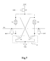
- FIG. 7 is a circuit diagram illustrating a nonvolatile memory device according to another embodiment of the present invention.
- the nonvolatile memory device comprises a flip-flop unit 30 , resistive memory devices R 3 and R 4 , an access controller including NMOS transistors N 8 and N 9 , and a driver which is a NMOS transistor N 10 .
- the flip-flop unit 30 comprises a NMOS latch including NMOS transistors N 6 and N 7 . Gate input signals of the NMOS transistors N 6 and N 7 are connected to the resistive memory devices R 3 and R 4 with a positive feedback type circuit.
- the resistive memory device R 3 which is connected to a common drain of the NMOS transistors N 6 and N 10 , stores nonvolatile data.
- the resistive memory device R 4 which is connected to a common drain of the NMOS transistors N 7 and N 10 , stores nonvolatile data.
- the access controller comprises NMOS transistors N 8 and N 9 for controlling connection of bitlines BIT and /BIT depending on an enable state of a wordline WL.
- the NMOS transistor N 8 having a gate connected to the wordline WL is connected between the bitline BIT and a drain of the NMOS transistor N 6 .
- the NMOS transistor N 9 having a gate connected to the wordline WL is connected between the bitline /BIT and a drain of the NMOS transistor N 7 .
- the driver comprises a NMOS transistor N 10 .
- the NMOS transistor N 10 connected between a power voltage VCC terminal and the resistive memory devices R 3 and R 4 , has a gate to receive a write/read control signal WRC.
- FIG. 8 is a circuit diagram illustrating a nonvolatile memory device according to another embodiment of the present invention.
- gate input signals of NMOS transistors N 6 and N 7 are connected to resistive memory devices R 3 and R 4 with a negative feedback type circuit.
- the nonvolatile memory device of FIG. 8 does not comprise a NMOS transistor N 10 like that of FIG. 7 .
- the explanation of the rest configuration and operation is omitted because it is similar to that of FIG. 7 .
- FIG. 9 is a circuit diagram illustrating a nonvolatile memory device according to another embodiment of the present invention.
- the nonvolatile memory device of FIG. 9 comprises a flip-flop unit 30 , resistive memory devices R 3 and R 4 , and an access controller including NMOS transistors N 8 and N 9 .
- the flip-flop unit 30 comprises a NMOS latch including NMOS transistors N 6 and N 7 . Gate input signals of the NMOS transistors N 6 and N 7 are connected to the resistive memory devices R 3 and R 4 with a positive feedback type circuit.
- the resistive memory device R 3 connected between a terminal of the NMOS transistor P 8 and a drain of the NMOS transistor N 6 , stores nonvolatile data.
- the resistive memory device R 4 connected between a terminal of the NMOS transistor P 9 and a drain of the NMOS transistor N 7 , stores nonvolatile data.
- the access controller including the NMOS transistors N 8 and N 9 controls a connection of bitlines BIT and /BIT depending on an enable state of a wordline WL.
- the NMOS transistor N 8 having a gate connected to the wordline WL is connected between the bitline BIT and a terminal of the resistive memory device R 3 .
- the NMOS transistor N 9 having a gate connected to the wordline WL is connected between the bitline /BIT and a terminal of the resistive memory device R 4 .
- a PCM device is exemplified as a resistive memory device in the above embodiments
- a MTJ (Magnetic Tunneling Junction) or GMR (Giant Magnetic Resistive) device can be used as a resistive memory device alternatively.
- a nonvolatile memory device can be utilized as a nonvolatile programmable gate memory device such as a FPGA (Field Programmable Gate Array).
- FPGA Field Programmable Gate Array
- a nonvolatile memory device can be embodied using a resistive memory device in an embodiment of the present invention.
- a programmable register is applied to a memory chip in order to program data for regulating redundancy and reference with a software type, thereby improving reliability of the chip.
Abstract
The present invention relates to a nonvolatile memory device, and more specifically, to a programmable nonvolatile logic switch memory (register) device using a resistive memory device. The programmable nonvolatile register uses a logic switch or a nonvolatile resistive memory device whose resistive state can be set by flowing a controlled current through it.
Description
1. Field of the Invention
The present invention relates to a nonvolatile memory device, and more specifically, to a programmable nonvolatile logic switch memory (register) using a resistive memory device.
2. Description of the Prior Art
Generally, nonvolatile memory such as magnetic memory and phase change memory (PCM) has a data processing speed similar to that of volatile RAM (Random Access Memory). When power is off, data of the nonvolatile memory are preserved.
A volatile logic switch SW1 connects a node B with a node C in response to a control signal applied to a gate input terminal A. The gate input terminal A of the volatile logic switch SW1 has no memory device for storing previous and current data. As a result, data stored in the memory device are not preserved when power is off.
The flip-flop volatile memory device comprises a flip-flop unit including PMOS transistors P1 and P2, and NMOS transistors N1 and N2. The flip-flop volatile memory device further comprises NMOS transistors N3 and N4 for storing data applied from bitlines BIT and /BIT in the flip-flop unit depending on an enable state of a wordline WL.
The conventional flip-flop volatile memory device can store data in both terminals of the flip-flop unit with a static state when power is on. However, the data stored in the terminals both of the flip-flop unit are destroyed when power is off.
Nonvolatile memory devices have been developed to overcome the above problem of the conventional volatile memory device. FIGS. 3 a to 3 d are diagrams illustrating a conventional phase change memory (PCM) device.
The PCM device 4 comprises a phase change layer (PCL) 2 of phase change material for receiving voltage and current between a top electrode 1 and a bottom electrode 3. The voltage and current induce high temperature in the PCL 2, thereby changing electric conductivity of the PCL 2.
As shown in FIG. 3 c, if low current of less than a threshold value flows in the PCM device 4, the PCL 2 has a proper temperature to be crystallized. Thus, the PCL 2 comes to have high resistance.
Referring to FIG. 3 d, if high current of more than a threshold value flows in the PCM device 4, the PCL 2 has a temperature over a melting point of the phase change material. Thus, the PCL 2 becomes uncrystallized to have low resistance.
The PCM device 4 can store nonvolatile data corresponding to the two resistances.
Accordingly, it is an object of the present invention to provide a programmable nonvolatile logic switch memory (register) device using a nonvolatile resistance memory device.
In an embodiment, there is provided a nonvolatile memory device comprising a write/read controller, a nonvolatile resistive memory device and a logic switch. The write/read controller selectively controls write/read control signals enabled in a write mode. As used herein, a nonvolatile resistive memory device is a circuit element that stores different logic values in the level of electrical resistance of one or more circuit elements, such that the states of resistance of the element or elements can be changed or set (e.g., set to a high resistance or set to a low resistance) by controlling the amount of current that passes through the device when the write/read control signals are enabled. The logic switch selects switching states depending on the different logic values pre-stored in the nonvolatile resistive memory device when the write/read control signals are disabled.
In an embodiment, there is also provided a nonvolatile memory device comprising a flip-flop unit, a nonvolatile resistive memory device, an access controller and a current supply unit. The flip-flop unit includes a PMOS latch and a NMOS latch, and latch the opposite data. The nonvolatile resistive memory device, which is connected between the PMOS latch and the NMOS latch, stores different logic values depending on states of resistance changed by the amount of current. The access controller controls connection of a bitline and the flip-flop unit depending on an enable state of a wordline. The current supply unit supplies current for changing data stored in the resistive memory device when the write/read control signals are enabled.
In an embodiment, there is also provided a nonvolatile memory device comprising a flip-flop unit, a nonvolatile resistive memory device and an access controller. The flip-flop unit includes a NMOS latch for latching opposite data. The nonvolatile resistive memory device, which is connected between a power voltage terminal and the flip-flop unit, stores different logic values depending on states of resistance changed by the amount of current. The access controller controls a connection of a bitline to the flip-flop unit depending on an enable state of a wordline.
In an embodiment, there is provided a nonvolatile memory device comprising a flip-flop unit, an access controller and a nonvolatile resistive memory device. The flip-flop unit includes a NMOS latch for latching opposite data. The access controller controls a connection of a bitline to the flip-flop unit depending on an enable state of a wordline. The nonvolatile resistive memory device, which is connected between the flip-flop unit and the access controller, stores different logic values depending on states of resistance changed by the amount of current.
The present invention will be described in detail with reference to the attached drawings.
In an embodiment, the nonvolatile memory device comprises a write/read controller 20, resistance memory devices R1 and R2, and a logic switch SW2.
The write/read controller 20 selectively outputs a write/read control signal WRC1 in response to a write control signal WRC2 inputted into a gate of a NMOS transistor N5 and a write control signal WRC3 inputted into a gate of a PMOS transistor P3. The write control signal WRC2 has an opposite phase to that of the write control signal WRC3.
The resistive memory device R1 is connected between a node D and a node F. The resistive memory device R2 is connected between a node E and a node F. The node F is connected to a gate of the logic switch SW2.
Next, the write operation according to an embodiment of the present invention is described.
When the write control signal WRC2 inputted in the write/read controller 20 is at a high level, the NMOS transistor N5 is turned on. When the write control signal WRC3 is at a low level, the PMOS transistor P3 is turned on, and the write/read control signal WRC1 is outputted.
If current is applied between the nodes D and F, data is written in the resistive memory device R1. If current is applied between the nodes E and F, data is written in the resistive memory device R2.
The resistive memory devices R1 and R2 of FIG. 4 a may be represented like those in FIG. 4 b.
When the write control signal WRC2 is at a low level and the write control signal WRC3 is at a high level, the NMOS transistor N5 and the PMOS transistor P3 of the write/read controller 20 are all turned off. Here, when the resistive memory device R1 has a low resistance and the resistive memory device R2 has a high resistance, the states of the logic switch SW2 are determined depending on states of input signals through the input nodes D and E.
Table 1 shows the operation of the logic switch SW2 depending on input signals when low data is stored in the resistive memory device R1 and the high data is stored in the resistive memory device R2.
| TABLE 1 | ||||||
| D | E | R1 | R2 | SW2 | ||
| L | L | L | H | OFF | ||
| H | L | L | H | ON | ||
| L | H | L | H | OFF | ||
| H | H | L | H | ON | ||
When a high level signal is applied to the node D and a high or low level signal is applied to the node E, the logic switch SW2 is turned on to output a signal of the node ND1 into the node ND2.
On the other hand, when a low level signal is applied to the node D and a low or high level signal is a applied to the node E, the logic switch SW2 is turned off. As a result, the signal of the node ND1 is not outputted into the node ND2.
When the resistive memory device R1 has a high resistance and the resistive memory device R2 has a low resistance, the states of the logic switch SW2 are determined depending on states of input signals inputted through the input nodes D and E.
Table 2 shows the operation of the logic switch SW2 depending on the input signals when high data is stored in the resistive memory device R1 and low data is stored in the resistive memory device R2.
| TABLE 2 | ||||||
| D | E | R1 | R2 | SW2 | ||
| L | L | H | L | OFF | ||
| H | L | H | L | OFF | ||
| L | H | H | L | ON | ||
| H | H | H | L | ON | ||
When a high or low level signal is applied to the node D and a high level signal is applied to the node E, the logic switch SW2 is turned on to output a signal of the node ND1 into the node ND2.
When the high or low level signal is applied to the node D and a low level signal is applied to the node E, the logic switch SW2 is turned off. As a result, the signal of the node ND1 is not outputted into the node ND2.
In an embodiment, the nonvolatile memory device comprises a flip-flop unit 30, resistive memory devices R3 and R4, an access controller including NMOS transistors N8 and N9, and a current supply unit including PMOS transistors P6 and P7.
The flip-flop unit 30 comprises a NMOS latch including NMOS transistors N6 and N7, and a PMOS latch including PMOS transistors P4 and P5. The NMOS latch and the PMOS latch store opposite data.
The resistive memory device R3, which is connected to a common drain of the PMOS transistor P4 and the NMOS transistor N6, stores nonvolatile data. The resistive memory device R4, which is connected to a common drain of the PMOS transistor P5 and the NMOS transistor N7, stores nonvolatile data.
The access controller, including the NMOS transistors N8 and N9, controls a connection of bitlines BIT and /BIT depending on an enable state of a wordline WL. The NMOS transistor N8 having a gate connected to the wordline WL is connected between the bitline BIT and the drain of the NMOS transistor N6. The NMOS transistor N9 having a gate connected to the wordline WL is connected between the bitline /BIT and the drain of the NMOS transistor N7.
The current supply unit comprises PMOS transistor P6 and P7 for changing data stored in the resistive memory devices R3 and R4 in a write mode. The PMOS transistor P6 connected in parallel to the PMOS transistor P4 has a gate to receive a write/read control signal WRC. The PMOS transistor P7 connected in parallel to the PMOS transistor P5 has a gate to receive the write/read control signal WRC.
Gate input signals of the PMOS latch and the NMOS latch are connected to the resistive memory devices R3 and R4 with a positive feedback type circuit.
When the write/read control signal WRC is at a low level, the PMOS transistors P6 and P7 are turned on to apply a predetermined voltage to the bitlines BIT and /BIT. Then, a difference in current flowing in the resistive memory devices R3 and R4 is generated by a difference in voltages of the bitlines BIT and /BIT. As a result, the amount of heat applied to the resistive memory devices R3 and R4 is also differentiated.
Here, voltages of the bitlines BIT and /BIT are determined to generate heat in the resistive memory devices R3 and R4 over or below the melting point.
The embodiment shown in FIG. 6 is different from that of FIG. 5 in that gate input signals of the PMOS latch P4,P5 and the NMOS latch N6,N7 are connected to the resistive memory devices R3 and R4 with a negative feedback type circuit. The explanation of the rest configuration and operation is omitted because it is similar to that of FIG. 5.
In this embodiment, the nonvolatile memory device comprises a flip-flop unit 30, resistive memory devices R3 and R4, an access controller including NMOS transistors N8 and N9, and a driver which is a NMOS transistor N10.
The flip-flop unit 30 comprises a NMOS latch including NMOS transistors N6 and N7. Gate input signals of the NMOS transistors N6 and N7 are connected to the resistive memory devices R3 and R4 with a positive feedback type circuit.
The resistive memory device R3, which is connected to a common drain of the NMOS transistors N6 and N10, stores nonvolatile data. The resistive memory device R4, which is connected to a common drain of the NMOS transistors N7 and N10, stores nonvolatile data.
The access controller comprises NMOS transistors N8 and N9 for controlling connection of bitlines BIT and /BIT depending on an enable state of a wordline WL. The NMOS transistor N8 having a gate connected to the wordline WL is connected between the bitline BIT and a drain of the NMOS transistor N6. The NMOS transistor N9 having a gate connected to the wordline WL is connected between the bitline /BIT and a drain of the NMOS transistor N7.
The driver comprises a NMOS transistor N10. The NMOS transistor N10, connected between a power voltage VCC terminal and the resistive memory devices R3 and R4, has a gate to receive a write/read control signal WRC.
In the nonvolatile memory device of FIG. 8 , gate input signals of NMOS transistors N6 and N7 are connected to resistive memory devices R3 and R4 with a negative feedback type circuit. The nonvolatile memory device of FIG. 8 does not comprise a NMOS transistor N10 like that of FIG. 7. The explanation of the rest configuration and operation is omitted because it is similar to that of FIG. 7.
The nonvolatile memory device of FIG. 9 comprises a flip-flop unit 30, resistive memory devices R3 and R4, and an access controller including NMOS transistors N8 and N9.
The flip-flop unit 30 comprises a NMOS latch including NMOS transistors N6 and N7. Gate input signals of the NMOS transistors N6 and N7 are connected to the resistive memory devices R3 and R4 with a positive feedback type circuit.
The resistive memory device R3, connected between a terminal of the NMOS transistor P8 and a drain of the NMOS transistor N6, stores nonvolatile data. The resistive memory device R4, connected between a terminal of the NMOS transistor P9 and a drain of the NMOS transistor N7, stores nonvolatile data.
The access controller including the NMOS transistors N8 and N9 controls a connection of bitlines BIT and /BIT depending on an enable state of a wordline WL. The NMOS transistor N8 having a gate connected to the wordline WL is connected between the bitline BIT and a terminal of the resistive memory device R3. The NMOS transistor N9 having a gate connected to the wordline WL is connected between the bitline /BIT and a terminal of the resistive memory device R4.
Although a PCM device is exemplified as a resistive memory device in the above embodiments, a MTJ (Magnetic Tunneling Junction) or GMR (Giant Magnetic Resistive) device can be used as a resistive memory device alternatively.
Additionally, a nonvolatile memory device according to an embodiment of the present invention can be utilized as a nonvolatile programmable gate memory device such as a FPGA (Field Programmable Gate Array).
As discussed earlier, a nonvolatile memory device can be embodied using a resistive memory device in an embodiment of the present invention. Such a programmable register is applied to a memory chip in order to program data for regulating redundancy and reference with a software type, thereby improving reliability of the chip.
While the invention is susceptible to various modifications and alternative forms, specific embodiments have been shown by way of example in the drawings and described in detail herein. However, it should be understood that the invention is not limited to the particular forms disclosed. Rather, the invention covers all modifications, equivalents, and alternatives falling within the spirit and scope of the invention as defined in the appended claims.
Claims (23)
1. A nonvolatile memory device having a write mode of operation, comprising:
a write/read controller configured to selectively control write/read control signals enabled in the write mode;
a nonvolatile resistive memory device coupled to receive write/read control signals from the write/read controller; and
a logic switch having two or more switching states configured to select among the switching states depending on a logic value stored in the nonvolatile resistive memory device when the write/read control signals are disabled.
2. The nonvolatile memory device according to claim 1 , wherein the write/read controller comprises:
a first NMOS transistor controlled by a first write control signal;
a first PMOS transistor connected in parallel to the first NMOS transistor and controlled by a second write control signal having an opposite phase to the first write control signal.
3. The nonvolatile memory device according to claim 1 , wherein the nonvolatile resistive memory device comprises:
a first resistive memory device having a resistive state connected between a first input node and an output node of the write/read controller; and
a second resistive memory device having a settable resistive state connected between a second input node and the output node of the write/read controller.
4. The nonvolatile memory device according to claim 3 , wherein the selection of a switching state of the logic switch is determined based on a state of a first input signal inputted into the first resistive memory device when the first resistive memory device is set at a low resistance state and the second resistive memory device is set at a high resistance state, and
the selection of a switching state of the logic switch is determined based on a state of a second input signal inputted into the second resistive memory device when the first resistive memory device is set at a high resistance state and the second resistive memory device is set at a low resistance state.
5. The nonvolatile memory device according to claim 4 , wherein each of the first and the second resistive memory devices comprises:
a first electrode connected to one of the first input node or the second input node;
a second electrode connected to an output node of the write/read controller; and
a phase change layer formed between the first electrode and the second electrode.
6. The nonvolatile memory device according to claim 1 , wherein the nonvolatile resistive memory device comprises at least one of a phase change memory device, a magnetoresistive device and a metal memory device.
7. A nonvolatile memory device, comprising:
a flip-flop unit comprising a PMOS latch configured to latch a datum and a NMOS latch configured to latch a complement of the datum;
a nonvolatile resistive memory device connected between the PMOS latch and the NMOS latch;
an access controller for controlling a connection of a bitline and the flip-flop unit depending on an enable state of a wordline; and
a current supply unit configured to supply current for changing data stored in the nonvolatile resistive memory device when write/read control signals are enabled.
8. The nonvolatile memory device according to claim 7 , wherein gate input signals of the PMOS latch and the NMOS latch are connected to the nonvolatile resistive memory device with either a positive feedback type circuit or a negative feedback type circuit.
9. The nonvolatile memory device according to claim 7 , wherein the nonvolatile resistive memory device comprises a first resistive memory device and a second resistive memory device, each of the first and second resistive memory devices configured to store different logic values depending on a difference in an amount of current generated by a voltage applied to the bitline when the write/read control signals are enabled.
10. The nonvolatile memory device according to claim 9 , wherein each of the first resistive memory device and the second resistive memory device comprises:
a first electrode connected to the PMOS latch;
a second electrode connected to the NMOS latch; and
a phase change layer formed between the first electrode and the second electrode.
11. The device according to claim 7 , wherein the current supply unit comprises a first PMOS transistor and a second PMOS transistor, each of the first and second PMOS transistors configured to be connected in parallel to the PMOS latch and to have a gate configured to receive the write/read control signals.
12. A nonvolatile memory device, comprising:
a flip-flop unit comprising a NMOS latch for latching data;
a nonvolatile resistive memory device, connected between a power voltage terminal and the flip-flop unit; and
an access controller for controlling a connection of a bitline and the flip-flop unit depending on an enable state of a wordline.
13. The nonvolatile memory device according to claim 12 , wherein the NMOS latch comprises a first NMOS transistor and a second NMOS transistor configured to be connected between the resistive memory device and a ground voltage terminal with a latch type circuit, and
gate input signals of the first and the second NMOS transistors are connected to the nonvolatile resistive memory device with either a positive feedback type circuit or a negative feedback type circuit.
14. The nonvolatile memory device according to claim 12 , wherein the nonvolatile resistive memory device comprises a first resistive memory device and a second resistive memory device, each of the first and second resistive memory device configured to store different logic values depending on a difference in an amount of current generated by a voltage applied to the bitline.
15. The nonvolatile memory device according to claim 14 , wherein each of the first and the second resistive memory devices comprises:
a first electrode connected to the power voltage terminal;
a second electrode connected to the NMOS latch; and
a phase change layer formed between the first electrode and the second electrode.
16. The nonvolatile memory device according to claim 12 , further comprising a driver circuit configured to supply a power voltage to the nonvolatile resistive memory device when write/read control signals are enabled.
17. A nonvolatile memory device, comprising:
a flip-flop unit including a NMOS latch for latching a datum and its complement;
an access controller for controlling a connection of a bitline to the flip-flop unit depending on an enable state of a wordline; and
a phase change memory device connected between the flip-flop unit and the access controller.
18. The nonvolatile memory device according to claim 17 , wherein the NMOS latch comprises a first NMOS transistor and a second NMOS transistor configured to be connected between the phase change memory device and a ground voltage terminal with a latch circuit, and
gate input signals of the first and the second NMOS transistors are connected to the phase change memory device with a positive feedback type circuit.
19. The nonvolatile memory device according to claim 17 , wherein the phase change memory device comprises a first phase change memory device and a second phase change memory device, each phase change memory device configured to store different logic values depending on a difference in an amount of current generated by a voltage applied to the bitline.
20. The nonvolatile memory device according to claim 19 , wherein each of the first and the second phase change memory device comprises:
a first electrode connected to the access controller;
a second electrode connected to the NMOS latch; and
a phase change layer formed between the first electrode and the second electrode.
21. An electronic device, comprising:
a write/read controller means for selectively controlling write/read control signals enabled in a write mode;
a resistive memory means for storing data based on states of resistance that can be changed by passing an amount of current through the means when the write/read control signals are enabled; and
a logic switch means for selecting among switching states based on logic values stored in the resistive memory means when the write/read control signals are disabled.
22. An electronic device comprising:
a means for latching data;
a phase change memory means for storing data as states of resistance that can be set by an applied electrical current, the phase change memory means being coupled to the means for latching data;
an access controller means for connecting a data input to the means for latching data in response to an enable state of a wordline; and
a current supply means for supplying current to the phase change memory means for changing a resistive state in response to a write control signal.
23. A method for storing data in a memory, comprising the steps of:
selectively controlling write/read control signals enabled in a write mode of a controller;
storing data in a resistive memory based on states of resistance that can be changed by passing an amount of current through the resistive memory when the write/read control signals are enabled; and
selecting among switching states based on logic values stored in the resistive memory when the write/read control signals are disabled.
Applications Claiming Priority (2)
| Application Number | Priority Date | Filing Date | Title |
|---|---|---|---|
| KR10-2002-0086704A KR100479810B1 (en) | 2002-12-30 | 2002-12-30 | Non-volatile memory device |
| KR2002-86704 | 2002-12-30 |
Publications (2)
| Publication Number | Publication Date |
|---|---|
| US20040125643A1 US20040125643A1 (en) | 2004-07-01 |
| US6944050B2 true US6944050B2 (en) | 2005-09-13 |
Family
ID=32588934
Family Applications (1)
| Application Number | Title | Priority Date | Filing Date |
|---|---|---|---|
| US10/629,903 Expired - Lifetime US6944050B2 (en) | 2002-12-30 | 2003-07-30 | Nonvolatile memory device |
Country Status (6)
| Country | Link |
|---|---|
| US (1) | US6944050B2 (en) |
| JP (2) | JP4615839B2 (en) |
| KR (1) | KR100479810B1 (en) |
| CN (1) | CN1224107C (en) |
| DE (1) | DE10335065A1 (en) |
| TW (1) | TWI239013B (en) |
Cited By (25)
| Publication number | Priority date | Publication date | Assignee | Title |
|---|---|---|---|---|
| US20040179394A1 (en) * | 2003-03-10 | 2004-09-16 | Ovshinsky Stanford R. | Secured phase-change devices |
| US20050128791A1 (en) * | 2003-12-13 | 2005-06-16 | Hynix Semiconductor Inc. | Phase change resistor cell and nonvolatile memory device using the same |
| US20060067098A1 (en) * | 2004-09-30 | 2006-03-30 | Richard Ferrant | Content addressable memory cell including resistive memory elements |
| US20070047160A1 (en) * | 2005-08-24 | 2007-03-01 | Philipp Jan B | Reprogrammable switch using phase change material |
| US20070146012A1 (en) * | 2005-11-03 | 2007-06-28 | Cswitch Corp. A California Corporation | Reconfigurable logic structures |
| US20070177432A1 (en) * | 2006-01-27 | 2007-08-02 | Spall Edward J | Phase change memory latch |
| US20080007986A1 (en) * | 2006-07-04 | 2008-01-10 | Samsung Electronics Co., Ltd. | One-time programmable devices including chalcogenide material, electronic systems including the same and methods of operating the same |
| US20080080231A1 (en) * | 2006-09-28 | 2008-04-03 | Kabushiki Kaisha Toshiba | Nonvolatile latch circuit and nonvolatile flip-flop circuit |
| US20080080227A1 (en) * | 2006-09-29 | 2008-04-03 | Alexander Duch | Tunable resistor and method for operating a tunable resistor |
| US20080151610A1 (en) * | 2004-06-04 | 2008-06-26 | Micron Technology, Inc. | Spintronic devices with integrated transistors |
| US20100073991A1 (en) * | 2008-09-25 | 2010-03-25 | Kabushiki Kaisha Toshiba | Storage apparatus |
| US20100214827A1 (en) * | 2004-09-30 | 2010-08-26 | Nxp B.V. | Integrated Circuit with Memory Cells Comprising a Programmable Resistor and Method for Addressing Memory Cells Comprising a Programmable Resistor |
| US7796417B1 (en) * | 2008-04-14 | 2010-09-14 | Altera Corporation | Memory circuits having programmable non-volatile resistors |
| US20110133778A1 (en) * | 2009-12-09 | 2011-06-09 | Samsung Electronics Co., Ltd. | Non-volatile logic circuits, integrated circuits including the non-volatile logic circuits, and methods of operating the integrated circuits |
| US20110216573A1 (en) * | 2010-03-05 | 2011-09-08 | Kabushiki Kaisha Toshiba | Semiconductor integrated circuit |
| US8531866B2 (en) | 2009-03-19 | 2013-09-10 | Kabushiki Kaisha Toshiba | Nonvolatile memories and reconfigurable circuits |
| US8537597B2 (en) | 2011-11-30 | 2013-09-17 | Kabushiki Kaisha Toshiba | Semiconductor memory device |
| US8560902B1 (en) | 2012-07-18 | 2013-10-15 | International Business Machines Corporation | Writing scheme for phase change material-content addressable memory |
| US20130286721A1 (en) * | 2012-04-25 | 2013-10-31 | Industry Academic Cooperation, Yonsei University | Low sensing current non-volatile flip-flop |
| US9378807B2 (en) * | 2014-07-30 | 2016-06-28 | Winbond Electronics Corp. | Non-volatile static random access memory circuits |
| US9543006B2 (en) * | 2015-05-25 | 2017-01-10 | Ningbo Advanced Memory Technology Corporation | Non-volatile memory cell and non-volatile memory device |
| WO2017196369A1 (en) * | 2016-05-13 | 2017-11-16 | Adesto Technologies Corporation | Static random access memories with programmable impedance elements and methods and devices including the same |
| TWI635488B (en) * | 2013-09-20 | 2018-09-11 | 國立大學法人東北大學 | Memory cell and storage device |
| US20200265892A1 (en) * | 2019-02-19 | 2020-08-20 | Samsung Electronics Co., Ltd. | 2t2r binary weight cell with high on/off ratio background |
| US11182686B2 (en) * | 2019-03-01 | 2021-11-23 | Samsung Electronics Co., Ltd | 4T4R ternary weight cell with high on/off ratio background |
Families Citing this family (62)
| Publication number | Priority date | Publication date | Assignee | Title |
|---|---|---|---|---|
| DE10320701A1 (en) | 2003-05-08 | 2004-12-23 | Siemens Ag | Component with a circuit arrangement that can be configured in terms of its functionality, in particular logic circuit arrangement |
| FR2871921A1 (en) * | 2004-06-16 | 2005-12-23 | St Microelectronics Sa | MEMORY ARCHITECTURE WITH SEGMENTED WRITING LINES |
| US7209383B2 (en) * | 2004-06-16 | 2007-04-24 | Stmicroelectronics, Inc. | Magnetic random access memory array having bit/word lines for shared write select and read operations |
| US7372728B2 (en) * | 2004-06-16 | 2008-05-13 | Stmicroelectronics, Inc. | Magnetic random access memory array having bit/word lines for shared write select and read operations |
| US7301800B2 (en) * | 2004-06-30 | 2007-11-27 | Stmicroelectronics, Inc. | Multi-bit magnetic random access memory element |
| US7136298B2 (en) | 2004-06-30 | 2006-11-14 | Stmicroelectronics, Inc. | Magnetic random access memory array with global write lines |
| US7079415B2 (en) * | 2004-06-30 | 2006-07-18 | Stmicroelectronics, Inc. | Magnetic random access memory element |
| US7106621B2 (en) * | 2004-06-30 | 2006-09-12 | Stmicroelectronics, Inc. | Random access memory array with parity bit structure |
| US7336525B2 (en) * | 2004-10-18 | 2008-02-26 | Kabushiki Kaisha Toshiba | Nonvolatile memory for logic circuits |
| JP4783002B2 (en) * | 2004-11-10 | 2011-09-28 | 株式会社東芝 | Semiconductor memory device |
| KR100576369B1 (en) * | 2004-11-23 | 2006-05-03 | 삼성전자주식회사 | Method for programming a non-volatile memory device employing a transition metal oxide layer as a data storage material layer |
| US7242218B2 (en) * | 2004-12-02 | 2007-07-10 | Altera Corporation | Techniques for combining volatile and non-volatile programmable logic on an integrated circuit |
| US7262639B2 (en) * | 2005-01-21 | 2007-08-28 | Broadcom Corporation | High-speed comparator |
| DE102005024897A1 (en) * | 2005-05-31 | 2006-12-07 | Infineon Technologies Ag | Non-volatile memory cell e.g. flash memory cell, for semiconductor device, has transistors reducing leakage currents that flow through non-volatile programmable resistors, respectively |
| DE102005030143B4 (en) * | 2005-06-28 | 2008-10-30 | Qimonda Ag | Memory element for non-volatile storage using resistive elements |
| US7319608B2 (en) * | 2005-06-30 | 2008-01-15 | International Business Machines Corporation | Non-volatile content addressable memory using phase-change-material memory elements |
| DE102005036066B3 (en) * | 2005-08-01 | 2006-09-21 | Siemens Ag | Programmable logic device component, has switching section including n-channel and p-channel transistors switched as inverter circuit to amplify voltage strokes between data line blocking/releasing switching section and voltage divider |
| JP4760225B2 (en) * | 2005-08-26 | 2011-08-31 | ソニー株式会社 | Storage device |
| US7679950B2 (en) * | 2005-08-24 | 2010-03-16 | Infineon Technologies Ag | Integrated circuit having a switch |
| US7741636B2 (en) * | 2006-01-09 | 2010-06-22 | Macronix International Co., Ltd. | Programmable resistive RAM and manufacturing method |
| KR100868035B1 (en) * | 2006-03-13 | 2008-11-10 | 키몬다 아게 | Memory circuit, method for operating a memory circuit, memory device and method for producing a memory device |
| US20070247196A1 (en) * | 2006-04-07 | 2007-10-25 | Thomas Niedermeier | Circuit and method for configuring a circuit |
| JP4909705B2 (en) * | 2006-10-20 | 2012-04-04 | 株式会社東芝 | Semiconductor integrated circuit device |
| US7728622B2 (en) * | 2007-03-29 | 2010-06-01 | Qualcomm Incorporated | Software programmable logic using spin transfer torque magnetoresistive random access memory |
| WO2009031231A1 (en) * | 2007-09-07 | 2009-03-12 | Renesas Technology Corp. | Semiconductor device |
| KR100858688B1 (en) * | 2007-12-06 | 2008-09-16 | 한양대학교 산학협력단 | Non volatile memory device and the reading method of the same |
| US7760538B1 (en) * | 2008-03-04 | 2010-07-20 | Xilinx, Inc. | Non-volatile SRAM cell |
| KR20100039593A (en) | 2008-10-08 | 2010-04-16 | 삼성전자주식회사 | Data communication system for measuring resist distribution of memory cell and semiconductor system having the same |
| US8130538B2 (en) * | 2009-01-15 | 2012-03-06 | Altera Corporation | Non-volatile memory circuit including voltage divider with phase change memory devices |
| US8400822B2 (en) * | 2010-03-22 | 2013-03-19 | Qualcomm Incorporated | Multi-port non-volatile memory that includes a resistive memory element |
| TWI565001B (en) | 2010-07-28 | 2017-01-01 | 半導體能源研究所股份有限公司 | Semiconductor device and method for driving the same |
| JP5092001B2 (en) * | 2010-09-29 | 2012-12-05 | 株式会社東芝 | Semiconductor integrated circuit |
| FR2970589B1 (en) * | 2011-01-19 | 2013-02-15 | Centre Nat Rech Scient | VOLATILE MEMORY CELL / NON VOLATILE |
| FR2970592B1 (en) | 2011-01-19 | 2013-02-15 | Centre Nat Rech Scient | PROGRAMMABLE VOLATILE / NON-VOLATILE MEMORY CELL |
| FR2970593B1 (en) | 2011-01-19 | 2013-08-02 | Centre Nat Rech Scient | COMPATIBLE VOLATILE / NON-VOLATILE MEMORY CELL |
| FR2976711B1 (en) * | 2011-06-15 | 2014-01-31 | Centre Nat Rech Scient | MEMORY CELL WITH VOLATILE AND NON-VOLATILE MEMORIZATION |
| FR2976712B1 (en) | 2011-06-15 | 2014-01-31 | Centre Nat Rech Scient | NON-VOLATILE MEMORY ELEMENT |
| FR2979737A1 (en) * | 2011-09-07 | 2013-03-08 | Commissariat Energie Atomique | Non-volatile static RAM cell for use in e.g. programmable logic circuit, has resistive storage units connected to storage nodes, where storage units are formed by zone of variable-resistance material arranged between electrodes |
| JP5733575B2 (en) * | 2011-09-12 | 2015-06-10 | 国立大学法人東北大学 | Semiconductor memory device |
| CN102436848A (en) * | 2011-12-22 | 2012-05-02 | 上海新储集成电路有限公司 | Phase change storage cell-based nonvolatile T flip-flop circuit and implementation method thereof |
| CN102496386B (en) * | 2011-12-22 | 2016-06-15 | 上海新储集成电路有限公司 | Based on the non-volatile JK flip-flop circuit of phase-change memory cell and realize method |
| US8680890B2 (en) | 2012-02-17 | 2014-03-25 | Taiwan Semiconductor Manufacturing Company, Ltd. | Sense amplifier |
| CN102594315A (en) * | 2012-02-17 | 2012-07-18 | 北京时代全芯科技有限公司 | Analog switch and redundant storage system adopting same |
| FR2990089B1 (en) * | 2012-04-27 | 2014-04-11 | Commissariat Energie Atomique | REPROGRAMMABLE LOGIC DEVICE RESISTANT TO RADIATION. |
| EP2979269A4 (en) * | 2013-03-27 | 2016-11-16 | Hewlett Packard Entpr Dev Lp | Non-volatile memory based synchronous logic |
| FR3004576B1 (en) | 2013-04-15 | 2019-11-29 | Commissariat A L'energie Atomique Et Aux Energies Alternatives | MEMORY CELL WITH NON-VOLATILE DATA STORAGE |
| FR3004577A1 (en) | 2013-04-15 | 2014-10-17 | Commissariat Energie Atomique | |
| JP6148534B2 (en) * | 2013-05-20 | 2017-06-14 | 株式会社東芝 | Non-volatile memory |
| FR3008219B1 (en) | 2013-07-05 | 2016-12-09 | Commissariat Energie Atomique | NON-VOLATILE MEMORY DEVICE |
| US9378812B2 (en) * | 2014-04-30 | 2016-06-28 | Freescale Semiconductor, Inc. | Non-volatile memory using bi-directional resistive elements |
| US9666276B2 (en) | 2014-04-30 | 2017-05-30 | Nxp Usa, Inc. | Non-volatile memory using bi-directional resistive elements |
| TWI550632B (en) * | 2014-10-30 | 2016-09-21 | 華邦電子股份有限公司 | Non-volatile static random access memory circuits |
| CN105590647B (en) * | 2014-11-13 | 2020-02-28 | 华邦电子股份有限公司 | Non-volatile static random access memory circuit |
| US10026476B2 (en) | 2014-11-25 | 2018-07-17 | Hewlett-Packard Development Company, L.P. | Bi-polar memristor |
| CN107431487B (en) * | 2015-03-12 | 2019-12-24 | 美高森美SoC公司 | FPGA based on compact ReRAM |
| JP2018513569A (en) | 2015-03-12 | 2018-05-24 | マイクロセミ エスオーシー コーポレーション | Compact ReRAM-based FPGA |
| CN104965801A (en) * | 2015-07-29 | 2015-10-07 | 国核自仪系统工程有限公司 | Dual-protection device for content of non-volatile memories and dual-protection method thereof |
| CN106611620B (en) * | 2015-10-27 | 2019-12-03 | 中芯国际集成电路制造(上海)有限公司 | Electric fuse bit location and its read-write method and electric fuse array |
| US10270451B2 (en) * | 2015-12-17 | 2019-04-23 | Microsemi SoC Corporation | Low leakage ReRAM FPGA configuration cell |
| TWI584290B (en) * | 2016-02-04 | 2017-05-21 | 新唐科技股份有限公司 | Non-volatile memory device and operating method thereof |
| US10211832B1 (en) * | 2017-12-05 | 2019-02-19 | Micron Technology, Inc. | Input buffer circuit |
| TWI805219B (en) * | 2022-02-10 | 2023-06-11 | 力晶積成電子製造股份有限公司 | Non-volatile static random access memory |
Citations (10)
| Publication number | Priority date | Publication date | Assignee | Title |
|---|---|---|---|---|
| US5566107A (en) | 1995-05-05 | 1996-10-15 | Micron Technology, Inc. | Programmable circuit for enabling an associated circuit |
| US5581501A (en) | 1995-08-17 | 1996-12-03 | Altera Corporation | Nonvolatile SRAM cells and cell arrays |
| US6175525B1 (en) | 1998-04-14 | 2001-01-16 | Honeywell Inc. | Non-volatile storage latch |
| US6191973B1 (en) | 1999-09-27 | 2001-02-20 | Motorola Inc. | Mram cam |
| US6269029B1 (en) * | 1999-06-29 | 2001-07-31 | Hyundai Electronics Industries, Co., Ltd. | Semi-conductor memory device |
| US6304477B1 (en) * | 2001-01-31 | 2001-10-16 | Motorola, Inc. | Content addressable magnetic random access memory |
| US6317359B1 (en) * | 1999-07-07 | 2001-11-13 | Iowa State University Research Foundation, Inc. | Non-volatile magnetic circuit |
| US6411545B1 (en) | 1999-11-19 | 2002-06-25 | John Millard And Pamela Ann Caywood 1989 Revokable Living Trust | Non-volatile latch |
| WO2002078007A1 (en) | 2001-03-23 | 2002-10-03 | Infineon Technologies Ag | Integrated logic circuit |
| US6714441B1 (en) * | 2002-09-17 | 2004-03-30 | Micron Technology, Inc. | Bridge-type magnetic random access memory (MRAM) latch |
Family Cites Families (3)
| Publication number | Priority date | Publication date | Assignee | Title |
|---|---|---|---|---|
| US4751677A (en) * | 1986-09-16 | 1988-06-14 | Honeywell Inc. | Differential arrangement magnetic memory cell |
| JP2001273758A (en) * | 2000-03-27 | 2001-10-05 | Sharp Corp | Magnetic memory |
| JP3711459B2 (en) * | 2002-06-05 | 2005-11-02 | 松下電器産業株式会社 | Driving method of nonvolatile memory circuit |
-
2002
- 2002-12-30 KR KR10-2002-0086704A patent/KR100479810B1/en not_active IP Right Cessation
-
2003
- 2003-07-30 US US10/629,903 patent/US6944050B2/en not_active Expired - Lifetime
- 2003-07-31 DE DE10335065A patent/DE10335065A1/en not_active Ceased
- 2003-07-31 TW TW092121016A patent/TWI239013B/en not_active IP Right Cessation
- 2003-08-13 CN CNB031534171A patent/CN1224107C/en not_active Expired - Fee Related
- 2003-09-26 JP JP2003336151A patent/JP4615839B2/en not_active Expired - Fee Related
-
2010
- 2010-04-07 JP JP2010088786A patent/JP5180986B2/en not_active Expired - Fee Related
Patent Citations (10)
| Publication number | Priority date | Publication date | Assignee | Title |
|---|---|---|---|---|
| US5566107A (en) | 1995-05-05 | 1996-10-15 | Micron Technology, Inc. | Programmable circuit for enabling an associated circuit |
| US5581501A (en) | 1995-08-17 | 1996-12-03 | Altera Corporation | Nonvolatile SRAM cells and cell arrays |
| US6175525B1 (en) | 1998-04-14 | 2001-01-16 | Honeywell Inc. | Non-volatile storage latch |
| US6269029B1 (en) * | 1999-06-29 | 2001-07-31 | Hyundai Electronics Industries, Co., Ltd. | Semi-conductor memory device |
| US6317359B1 (en) * | 1999-07-07 | 2001-11-13 | Iowa State University Research Foundation, Inc. | Non-volatile magnetic circuit |
| US6191973B1 (en) | 1999-09-27 | 2001-02-20 | Motorola Inc. | Mram cam |
| US6411545B1 (en) | 1999-11-19 | 2002-06-25 | John Millard And Pamela Ann Caywood 1989 Revokable Living Trust | Non-volatile latch |
| US6304477B1 (en) * | 2001-01-31 | 2001-10-16 | Motorola, Inc. | Content addressable magnetic random access memory |
| WO2002078007A1 (en) | 2001-03-23 | 2002-10-03 | Infineon Technologies Ag | Integrated logic circuit |
| US6714441B1 (en) * | 2002-09-17 | 2004-03-30 | Micron Technology, Inc. | Bridge-type magnetic random access memory (MRAM) latch |
Cited By (49)
| Publication number | Priority date | Publication date | Assignee | Title |
|---|---|---|---|---|
| US7085155B2 (en) * | 2003-03-10 | 2006-08-01 | Energy Conversion Devices, Inc. | Secured phase-change devices |
| US20040179394A1 (en) * | 2003-03-10 | 2004-09-16 | Ovshinsky Stanford R. | Secured phase-change devices |
| US20050128791A1 (en) * | 2003-12-13 | 2005-06-16 | Hynix Semiconductor Inc. | Phase change resistor cell and nonvolatile memory device using the same |
| US7038938B2 (en) * | 2003-12-13 | 2006-05-02 | Hynix Semiconductor Inc. | Phase change resistor cell and nonvolatile memory device using the same |
| US8164948B2 (en) | 2004-06-04 | 2012-04-24 | Micron Technology, Inc. | Spintronic devices with integrated transistors |
| US20120201076A1 (en) * | 2004-06-04 | 2012-08-09 | Micron Technology, Inc. | Spintronic devices with integrated transistors |
| US8503224B2 (en) * | 2004-06-04 | 2013-08-06 | Mircron Technology, Inc. | Spintronic devices with integrated transistors |
| US8004882B2 (en) * | 2004-06-04 | 2011-08-23 | Micron Technology, Inc. | Spintronic devices with integrated transistors |
| US20080151610A1 (en) * | 2004-06-04 | 2008-06-26 | Micron Technology, Inc. | Spintronic devices with integrated transistors |
| US7130206B2 (en) * | 2004-09-30 | 2006-10-31 | Infineon Technologies Ag | Content addressable memory cell including resistive memory elements |
| US8335103B2 (en) | 2004-09-30 | 2012-12-18 | Nxp B.V. | Integrated circuit with memory cells comprising a programmable resistor and method for addressing memory cells comprising a programmable resistor |
| US20060067098A1 (en) * | 2004-09-30 | 2006-03-30 | Richard Ferrant | Content addressable memory cell including resistive memory elements |
| US20100214827A1 (en) * | 2004-09-30 | 2010-08-26 | Nxp B.V. | Integrated Circuit with Memory Cells Comprising a Programmable Resistor and Method for Addressing Memory Cells Comprising a Programmable Resistor |
| US20070047160A1 (en) * | 2005-08-24 | 2007-03-01 | Philipp Jan B | Reprogrammable switch using phase change material |
| US7548448B2 (en) | 2005-08-24 | 2009-06-16 | Infineon Technologies Ag | Integrated circuit having a switch |
| US20070146012A1 (en) * | 2005-11-03 | 2007-06-28 | Cswitch Corp. A California Corporation | Reconfigurable logic structures |
| US7511532B2 (en) * | 2005-11-03 | 2009-03-31 | Cswitch Corp. | Reconfigurable logic structures |
| US20070177432A1 (en) * | 2006-01-27 | 2007-08-02 | Spall Edward J | Phase change memory latch |
| US7471554B2 (en) * | 2006-01-27 | 2008-12-30 | Ovonyx, Inc. | Phase change memory latch |
| US7656694B2 (en) | 2006-07-04 | 2010-02-02 | Samsung Electronics Co., Ltd. | Methods of programming one-time programmable devices including chalcogenide material |
| US20100090213A1 (en) * | 2006-07-04 | 2010-04-15 | Samsung Electronics Co., Ltd. | One-time programmable devices including chalcogenide material and electronic systems including the same |
| US20080007986A1 (en) * | 2006-07-04 | 2008-01-10 | Samsung Electronics Co., Ltd. | One-time programmable devices including chalcogenide material, electronic systems including the same and methods of operating the same |
| US7974115B2 (en) | 2006-07-04 | 2011-07-05 | Samsung Electronics Co., Ltd. | One-time programmable devices including chalcogenide material and electronic systems including the same |
| US7733145B2 (en) * | 2006-09-28 | 2010-06-08 | Kabushiki Kaisha Toshiba | Nonvolatile latch circuit and nonvolatile flip-flop circuit |
| US20080080231A1 (en) * | 2006-09-28 | 2008-04-03 | Kabushiki Kaisha Toshiba | Nonvolatile latch circuit and nonvolatile flip-flop circuit |
| US20080080227A1 (en) * | 2006-09-29 | 2008-04-03 | Alexander Duch | Tunable resistor and method for operating a tunable resistor |
| US7583527B2 (en) * | 2006-09-29 | 2009-09-01 | Infineon Technologies Ag | Tunable resistor and method for operating a tunable resistor |
| US7796417B1 (en) * | 2008-04-14 | 2010-09-14 | Altera Corporation | Memory circuits having programmable non-volatile resistors |
| US7903451B2 (en) * | 2008-09-25 | 2011-03-08 | Kabushiki Kaisha Toshiba | Storage apparatus including non-volatile SRAM |
| US20100073991A1 (en) * | 2008-09-25 | 2010-03-25 | Kabushiki Kaisha Toshiba | Storage apparatus |
| US8531866B2 (en) | 2009-03-19 | 2013-09-10 | Kabushiki Kaisha Toshiba | Nonvolatile memories and reconfigurable circuits |
| US20110133778A1 (en) * | 2009-12-09 | 2011-06-09 | Samsung Electronics Co., Ltd. | Non-volatile logic circuits, integrated circuits including the non-volatile logic circuits, and methods of operating the integrated circuits |
| US7961005B1 (en) | 2009-12-09 | 2011-06-14 | Samsung Electronics Co., Ltd. | Non-volatile logic circuits, integrated circuits including the non-volatile logic circuits, and methods of operating the integrated circuits |
| US20110216573A1 (en) * | 2010-03-05 | 2011-09-08 | Kabushiki Kaisha Toshiba | Semiconductor integrated circuit |
| US8243498B2 (en) | 2010-03-05 | 2012-08-14 | Kabushiki Kaisha Toshiba | Semiconductor integrated circuit |
| US8537597B2 (en) | 2011-11-30 | 2013-09-17 | Kabushiki Kaisha Toshiba | Semiconductor memory device |
| US8804403B2 (en) | 2011-11-30 | 2014-08-12 | Kabushiki Kaisha Toshiba | Semiconductor memory device |
| US9196337B2 (en) * | 2012-04-25 | 2015-11-24 | Qualcomm Incorporated | Low sensing current non-volatile flip-flop |
| US20130286721A1 (en) * | 2012-04-25 | 2013-10-31 | Industry Academic Cooperation, Yonsei University | Low sensing current non-volatile flip-flop |
| US8560902B1 (en) | 2012-07-18 | 2013-10-15 | International Business Machines Corporation | Writing scheme for phase change material-content addressable memory |
| US8943374B2 (en) | 2012-07-18 | 2015-01-27 | International Business Machines Corporation | Writing scheme for phase change material-content addressable memory |
| TWI635488B (en) * | 2013-09-20 | 2018-09-11 | 國立大學法人東北大學 | Memory cell and storage device |
| US9378807B2 (en) * | 2014-07-30 | 2016-06-28 | Winbond Electronics Corp. | Non-volatile static random access memory circuits |
| US9543006B2 (en) * | 2015-05-25 | 2017-01-10 | Ningbo Advanced Memory Technology Corporation | Non-volatile memory cell and non-volatile memory device |
| WO2017196369A1 (en) * | 2016-05-13 | 2017-11-16 | Adesto Technologies Corporation | Static random access memories with programmable impedance elements and methods and devices including the same |
| US10777268B2 (en) * | 2016-05-13 | 2020-09-15 | Adesto Technologies Corporation | Static random access memories with programmable impedance elements and methods and devices including the same |
| US20200265892A1 (en) * | 2019-02-19 | 2020-08-20 | Samsung Electronics Co., Ltd. | 2t2r binary weight cell with high on/off ratio background |
| US10872662B2 (en) * | 2019-02-19 | 2020-12-22 | Samsung Electronics Co., Ltd | 2T2R binary weight cell with high on/off ratio background |
| US11182686B2 (en) * | 2019-03-01 | 2021-11-23 | Samsung Electronics Co., Ltd | 4T4R ternary weight cell with high on/off ratio background |
Also Published As
| Publication number | Publication date |
|---|---|
| TW200411672A (en) | 2004-07-01 |
| US20040125643A1 (en) | 2004-07-01 |
| TWI239013B (en) | 2005-09-01 |
| JP5180986B2 (en) | 2013-04-10 |
| JP4615839B2 (en) | 2011-01-19 |
| JP2004213860A (en) | 2004-07-29 |
| CN1224107C (en) | 2005-10-19 |
| KR20040060169A (en) | 2004-07-06 |
| KR100479810B1 (en) | 2005-03-31 |
| JP2010176843A (en) | 2010-08-12 |
| DE10335065A1 (en) | 2004-07-22 |
| CN1512591A (en) | 2004-07-14 |
Similar Documents
| Publication | Publication Date | Title |
|---|---|---|
| US6944050B2 (en) | Nonvolatile memory device | |
| US7038938B2 (en) | Phase change resistor cell and nonvolatile memory device using the same | |
| US6128239A (en) | MRAM device including analog sense amplifiers | |
| JP5897337B2 (en) | Resistive memory device, layout structure thereof and sensing circuit | |
| EP1339066A1 (en) | Voltage biasing method of a resistive cross point memory cell arrray during sensing | |
| US20060050548A1 (en) | Semiconductor memory device capable of compensating for leakage current | |
| US8077501B2 (en) | Differential read and write architecture | |
| US7167389B2 (en) | Magnetic random access memory with a reference cell array and dummy cell arrays | |
| KR20050029013A (en) | Data read circuits for use in semiconductor memory and method therefore | |
| US8036015B2 (en) | Resistive memory | |
| US11120857B2 (en) | Low variability reference parameter generation for magnetic random access memory | |
| US6985389B2 (en) | Phase change based memory device and method for operating same | |
| KR100941505B1 (en) | Magnetic storage device using ferromagnetic tunnel junction element | |
| TW202240578A (en) | Midpoint sensing reference generation for stt-mram | |
| JP2007157206A (en) | Semiconductor integrated circuit apparatus | |
| US8335103B2 (en) | Integrated circuit with memory cells comprising a programmable resistor and method for addressing memory cells comprising a programmable resistor | |
| US20080137430A1 (en) | Low-voltage reading device in particular for mram memory | |
| US6785158B2 (en) | Device that makes it possible to selectively use nonvolatile memory as RAM or ROM | |
| US20040076029A1 (en) | Data sensing circuits and methods for magnetic memory devices | |
| KR950014090B1 (en) | Sense circuit of non-volatile memory device | |
| CN213459059U (en) | Nonvolatile memory device and voltage generator circuit | |
| US8472262B2 (en) | Sense amplifier for reading a crossbar memory array | |
| US11177010B1 (en) | Bitcell for data redundancy | |
| JP2004118922A (en) | Magnetic random access memory | |
| JP2000315382A (en) | Magnetic random access memory circuit |
Legal Events
| Date | Code | Title | Description |
|---|---|---|---|
| AS | Assignment |
Owner name: HYNIX SEMICONDUCTOR INC., KOREA, REPUBLIC OF Free format text: ASSIGNMENT OF ASSIGNORS INTEREST;ASSIGNORS:KANG, HEE BOK;PARK, YOUNG JIN;REEL/FRAME:015024/0219 Effective date: 20040130 |
|
| STCF | Information on status: patent grant |
Free format text: PATENTED CASE |
|
| FPAY | Fee payment |
Year of fee payment: 4 |
|
| FEPP | Fee payment procedure |
Free format text: PAYOR NUMBER ASSIGNED (ORIGINAL EVENT CODE: ASPN); ENTITY STATUS OF PATENT OWNER: LARGE ENTITY |
|
| FPAY | Fee payment |
Year of fee payment: 8 |
|
| FPAY | Fee payment |
Year of fee payment: 12 |