US6949286B2 - Radiation-absorbing layers for thermopile radiation detectors - Google Patents
Radiation-absorbing layers for thermopile radiation detectors Download PDFInfo
- Publication number
- US6949286B2 US6949286B2 US10/245,687 US24568702A US6949286B2 US 6949286 B2 US6949286 B2 US 6949286B2 US 24568702 A US24568702 A US 24568702A US 6949286 B2 US6949286 B2 US 6949286B2
- Authority
- US
- United States
- Prior art keywords
- film
- radiation
- particles
- percent
- absorbing layer
- Prior art date
- Legal status (The legal status is an assumption and is not a legal conclusion. Google has not performed a legal analysis and makes no representation as to the accuracy of the status listed.)
- Expired - Fee Related, expires
Links
- 230000005855 radiation Effects 0.000 title claims abstract description 66
- 239000002245 particle Substances 0.000 claims abstract description 92
- 239000000203 mixture Substances 0.000 claims abstract description 54
- 238000010276 construction Methods 0.000 claims abstract description 41
- 239000007787 solid Substances 0.000 claims abstract description 36
- 239000000463 material Substances 0.000 claims abstract description 34
- 229910052710 silicon Inorganic materials 0.000 claims abstract description 25
- 239000010703 silicon Substances 0.000 claims abstract description 25
- 239000010931 gold Substances 0.000 claims description 108
- PCHJSUWPFVWCPO-UHFFFAOYSA-N gold Chemical compound [Au] PCHJSUWPFVWCPO-UHFFFAOYSA-N 0.000 claims description 57
- 229910052737 gold Inorganic materials 0.000 claims description 57
- XUIMIQQOPSSXEZ-UHFFFAOYSA-N Silicon Chemical compound [Si] XUIMIQQOPSSXEZ-UHFFFAOYSA-N 0.000 claims description 24
- 239000012528 membrane Substances 0.000 claims description 18
- 239000004065 semiconductor Substances 0.000 claims description 15
- 239000000758 substrate Substances 0.000 claims description 15
- 230000001788 irregular Effects 0.000 claims description 12
- 238000012876 topography Methods 0.000 claims description 12
- 239000011521 glass Substances 0.000 claims description 6
- 229910052751 metal Inorganic materials 0.000 claims description 5
- 239000002184 metal Substances 0.000 claims description 5
- 238000010521 absorption reaction Methods 0.000 claims description 4
- 238000010292 electrical insulation Methods 0.000 claims description 4
- 150000002739 metals Chemical class 0.000 claims description 3
- ZOXJGFHDIHLPTG-UHFFFAOYSA-N Boron Chemical compound [B] ZOXJGFHDIHLPTG-UHFFFAOYSA-N 0.000 claims description 2
- OKTJSMMVPCPJKN-UHFFFAOYSA-N Carbon Chemical compound [C] OKTJSMMVPCPJKN-UHFFFAOYSA-N 0.000 claims description 2
- OAICVXFJPJFONN-UHFFFAOYSA-N Phosphorus Chemical compound [P] OAICVXFJPJFONN-UHFFFAOYSA-N 0.000 claims description 2
- 229910052785 arsenic Inorganic materials 0.000 claims description 2
- RQNWIZPPADIBDY-UHFFFAOYSA-N arsenic atom Chemical compound [As] RQNWIZPPADIBDY-UHFFFAOYSA-N 0.000 claims description 2
- 229910052796 boron Inorganic materials 0.000 claims description 2
- 229910052799 carbon Inorganic materials 0.000 claims description 2
- 239000002019 doping agent Substances 0.000 claims description 2
- 229910052698 phosphorus Inorganic materials 0.000 claims description 2
- 239000011574 phosphorus Substances 0.000 claims description 2
- 238000000034 method Methods 0.000 description 22
- VYPSYNLAJGMNEJ-UHFFFAOYSA-N Silicium dioxide Chemical compound O=[Si]=O VYPSYNLAJGMNEJ-UHFFFAOYSA-N 0.000 description 17
- 238000005530 etching Methods 0.000 description 10
- 238000012545 processing Methods 0.000 description 10
- DLYUQMMRRRQYAE-UHFFFAOYSA-N tetraphosphorus decaoxide Chemical compound O1P(O2)(=O)OP3(=O)OP1(=O)OP2(=O)O3 DLYUQMMRRRQYAE-UHFFFAOYSA-N 0.000 description 8
- 239000007788 liquid Substances 0.000 description 7
- 239000005360 phosphosilicate glass Substances 0.000 description 7
- 230000008569 process Effects 0.000 description 7
- 239000000377 silicon dioxide Substances 0.000 description 7
- 210000001787 dendrite Anatomy 0.000 description 6
- 235000012239 silicon dioxide Nutrition 0.000 description 6
- 230000005670 electromagnetic radiation Effects 0.000 description 5
- TWNQGVIAIRXVLR-UHFFFAOYSA-N oxo(oxoalumanyloxy)alumane Chemical compound O=[Al]O[Al]=O TWNQGVIAIRXVLR-UHFFFAOYSA-N 0.000 description 5
- 230000008901 benefit Effects 0.000 description 4
- 230000004044 response Effects 0.000 description 4
- 229910052797 bismuth Inorganic materials 0.000 description 3
- 239000007789 gas Substances 0.000 description 3
- 238000000059 patterning Methods 0.000 description 3
- 229910052814 silicon oxide Inorganic materials 0.000 description 3
- 238000003756 stirring Methods 0.000 description 3
- 239000000126 substance Substances 0.000 description 3
- QTBSBXVTEAMEQO-UHFFFAOYSA-N Acetic acid Chemical compound CC(O)=O QTBSBXVTEAMEQO-UHFFFAOYSA-N 0.000 description 2
- 239000002253 acid Substances 0.000 description 2
- LDDQLRUQCUTJBB-UHFFFAOYSA-N ammonium fluoride Chemical compound [NH4+].[F-] LDDQLRUQCUTJBB-UHFFFAOYSA-N 0.000 description 2
- 238000013459 approach Methods 0.000 description 2
- JCXGWMGPZLAOME-UHFFFAOYSA-N bismuth atom Chemical compound [Bi] JCXGWMGPZLAOME-UHFFFAOYSA-N 0.000 description 2
- 238000001312 dry etching Methods 0.000 description 2
- 230000008020 evaporation Effects 0.000 description 2
- 238000001704 evaporation Methods 0.000 description 2
- 239000001307 helium Substances 0.000 description 2
- 229910052734 helium Inorganic materials 0.000 description 2
- SWQJXJOGLNCZEY-UHFFFAOYSA-N helium atom Chemical compound [He] SWQJXJOGLNCZEY-UHFFFAOYSA-N 0.000 description 2
- 238000004519 manufacturing process Methods 0.000 description 2
- 238000012986 modification Methods 0.000 description 2
- 230000004048 modification Effects 0.000 description 2
- 230000003287 optical effect Effects 0.000 description 2
- 238000000206 photolithography Methods 0.000 description 2
- 230000001012 protector Effects 0.000 description 2
- 230000005679 Peltier effect Effects 0.000 description 1
- 229960000583 acetic acid Drugs 0.000 description 1
- 229910052782 aluminium Inorganic materials 0.000 description 1
- XAGFODPZIPBFFR-UHFFFAOYSA-N aluminium Chemical compound [Al] XAGFODPZIPBFFR-UHFFFAOYSA-N 0.000 description 1
- 229910052787 antimony Inorganic materials 0.000 description 1
- QZPSXPBJTPJTSZ-UHFFFAOYSA-N aqua regia Chemical compound Cl.O[N+]([O-])=O QZPSXPBJTPJTSZ-UHFFFAOYSA-N 0.000 description 1
- 239000012298 atmosphere Substances 0.000 description 1
- 230000009286 beneficial effect Effects 0.000 description 1
- 230000015572 biosynthetic process Effects 0.000 description 1
- 238000013461 design Methods 0.000 description 1
- 239000012362 glacial acetic acid Substances 0.000 description 1
- 239000012535 impurity Substances 0.000 description 1
- OCVXZQOKBHXGRU-UHFFFAOYSA-N iodine(1+) Chemical compound [I+] OCVXZQOKBHXGRU-UHFFFAOYSA-N 0.000 description 1
- 239000011159 matrix material Substances 0.000 description 1
- VBYZSBGMSZOOAP-UHFFFAOYSA-N molecular hydrogen hydrate Chemical compound O.[H][H] VBYZSBGMSZOOAP-UHFFFAOYSA-N 0.000 description 1
- 239000012299 nitrogen atmosphere Substances 0.000 description 1
- 238000004064 recycling Methods 0.000 description 1
- 230000009467 reduction Effects 0.000 description 1
- 239000000779 smoke Substances 0.000 description 1
- 238000009987 spinning Methods 0.000 description 1
- 238000012546 transfer Methods 0.000 description 1
- XLYOFNOQVPJJNP-UHFFFAOYSA-N water Substances O XLYOFNOQVPJJNP-UHFFFAOYSA-N 0.000 description 1
- 238000001039 wet etching Methods 0.000 description 1
Images


Classifications
-
- G—PHYSICS
- G01—MEASURING; TESTING
- G01J—MEASUREMENT OF INTENSITY, VELOCITY, SPECTRAL CONTENT, POLARISATION, PHASE OR PULSE CHARACTERISTICS OF INFRARED, VISIBLE OR ULTRAVIOLET LIGHT; COLORIMETRY; RADIATION PYROMETRY
- G01J5/00—Radiation pyrometry, e.g. infrared or optical thermometry
- G01J5/02—Constructional details
- G01J5/04—Casings
-
- C—CHEMISTRY; METALLURGY
- C04—CEMENTS; CONCRETE; ARTIFICIAL STONE; CERAMICS; REFRACTORIES
- C04B—LIME, MAGNESIA; SLAG; CEMENTS; COMPOSITIONS THEREOF, e.g. MORTARS, CONCRETE OR LIKE BUILDING MATERIALS; ARTIFICIAL STONE; CERAMICS; REFRACTORIES; TREATMENT OF NATURAL STONE
- C04B35/00—Shaped ceramic products characterised by their composition; Ceramics compositions; Processing powders of inorganic compounds preparatory to the manufacturing of ceramic products
- C04B35/01—Shaped ceramic products characterised by their composition; Ceramics compositions; Processing powders of inorganic compounds preparatory to the manufacturing of ceramic products based on oxide ceramics
- C04B35/14—Shaped ceramic products characterised by their composition; Ceramics compositions; Processing powders of inorganic compounds preparatory to the manufacturing of ceramic products based on oxide ceramics based on silica
-
- G—PHYSICS
- G01—MEASURING; TESTING
- G01J—MEASUREMENT OF INTENSITY, VELOCITY, SPECTRAL CONTENT, POLARISATION, PHASE OR PULSE CHARACTERISTICS OF INFRARED, VISIBLE OR ULTRAVIOLET LIGHT; COLORIMETRY; RADIATION PYROMETRY
- G01J5/00—Radiation pyrometry, e.g. infrared or optical thermometry
- G01J5/02—Constructional details
- G01J5/0225—Shape of the cavity itself or of elements contained in or suspended over the cavity
- G01J5/024—Special manufacturing steps or sacrificial layers or layer structures
-
- G—PHYSICS
- G01—MEASURING; TESTING
- G01J—MEASUREMENT OF INTENSITY, VELOCITY, SPECTRAL CONTENT, POLARISATION, PHASE OR PULSE CHARACTERISTICS OF INFRARED, VISIBLE OR ULTRAVIOLET LIGHT; COLORIMETRY; RADIATION PYROMETRY
- G01J5/00—Radiation pyrometry, e.g. infrared or optical thermometry
- G01J5/02—Constructional details
- G01J5/04—Casings
- G01J5/046—Materials; Selection of thermal materials
-
- G—PHYSICS
- G01—MEASURING; TESTING
- G01J—MEASUREMENT OF INTENSITY, VELOCITY, SPECTRAL CONTENT, POLARISATION, PHASE OR PULSE CHARACTERISTICS OF INFRARED, VISIBLE OR ULTRAVIOLET LIGHT; COLORIMETRY; RADIATION PYROMETRY
- G01J5/00—Radiation pyrometry, e.g. infrared or optical thermometry
- G01J5/02—Constructional details
- G01J5/08—Optical arrangements
- G01J5/0801—Means for wavelength selection or discrimination
-
- G—PHYSICS
- G01—MEASURING; TESTING
- G01J—MEASUREMENT OF INTENSITY, VELOCITY, SPECTRAL CONTENT, POLARISATION, PHASE OR PULSE CHARACTERISTICS OF INFRARED, VISIBLE OR ULTRAVIOLET LIGHT; COLORIMETRY; RADIATION PYROMETRY
- G01J5/00—Radiation pyrometry, e.g. infrared or optical thermometry
- G01J5/02—Constructional details
- G01J5/08—Optical arrangements
- G01J5/0853—Optical arrangements having infrared absorbers other than the usual absorber layers deposited on infrared detectors like bolometers, wherein the heat propagation between the absorber and the detecting element occurs within a solid
-
- C—CHEMISTRY; METALLURGY
- C04—CEMENTS; CONCRETE; ARTIFICIAL STONE; CERAMICS; REFRACTORIES
- C04B—LIME, MAGNESIA; SLAG; CEMENTS; COMPOSITIONS THEREOF, e.g. MORTARS, CONCRETE OR LIKE BUILDING MATERIALS; ARTIFICIAL STONE; CERAMICS; REFRACTORIES; TREATMENT OF NATURAL STONE
- C04B2235/00—Aspects relating to ceramic starting mixtures or sintered ceramic products
- C04B2235/02—Composition of constituents of the starting material or of secondary phases of the final product
- C04B2235/30—Constituents and secondary phases not being of a fibrous nature
- C04B2235/40—Metallic constituents or additives not added as binding phase
- C04B2235/408—Noble metals
-
- C—CHEMISTRY; METALLURGY
- C04—CEMENTS; CONCRETE; ARTIFICIAL STONE; CERAMICS; REFRACTORIES
- C04B—LIME, MAGNESIA; SLAG; CEMENTS; COMPOSITIONS THEREOF, e.g. MORTARS, CONCRETE OR LIKE BUILDING MATERIALS; ARTIFICIAL STONE; CERAMICS; REFRACTORIES; TREATMENT OF NATURAL STONE
- C04B2235/00—Aspects relating to ceramic starting mixtures or sintered ceramic products
- C04B2235/02—Composition of constituents of the starting material or of secondary phases of the final product
- C04B2235/30—Constituents and secondary phases not being of a fibrous nature
- C04B2235/42—Non metallic elements added as constituents or additives, e.g. sulfur, phosphor, selenium or tellurium
- C04B2235/422—Carbon
-
- C—CHEMISTRY; METALLURGY
- C04—CEMENTS; CONCRETE; ARTIFICIAL STONE; CERAMICS; REFRACTORIES
- C04B—LIME, MAGNESIA; SLAG; CEMENTS; COMPOSITIONS THEREOF, e.g. MORTARS, CONCRETE OR LIKE BUILDING MATERIALS; ARTIFICIAL STONE; CERAMICS; REFRACTORIES; TREATMENT OF NATURAL STONE
- C04B2235/00—Aspects relating to ceramic starting mixtures or sintered ceramic products
- C04B2235/02—Composition of constituents of the starting material or of secondary phases of the final product
- C04B2235/30—Constituents and secondary phases not being of a fibrous nature
- C04B2235/42—Non metallic elements added as constituents or additives, e.g. sulfur, phosphor, selenium or tellurium
- C04B2235/428—Silicon
-
- C—CHEMISTRY; METALLURGY
- C04—CEMENTS; CONCRETE; ARTIFICIAL STONE; CERAMICS; REFRACTORIES
- C04B—LIME, MAGNESIA; SLAG; CEMENTS; COMPOSITIONS THEREOF, e.g. MORTARS, CONCRETE OR LIKE BUILDING MATERIALS; ARTIFICIAL STONE; CERAMICS; REFRACTORIES; TREATMENT OF NATURAL STONE
- C04B2235/00—Aspects relating to ceramic starting mixtures or sintered ceramic products
- C04B2235/70—Aspects relating to sintered or melt-casted ceramic products
- C04B2235/80—Phases present in the sintered or melt-cast ceramic products other than the main phase
-
- Y—GENERAL TAGGING OF NEW TECHNOLOGICAL DEVELOPMENTS; GENERAL TAGGING OF CROSS-SECTIONAL TECHNOLOGIES SPANNING OVER SEVERAL SECTIONS OF THE IPC; TECHNICAL SUBJECTS COVERED BY FORMER USPC CROSS-REFERENCE ART COLLECTIONS [XRACs] AND DIGESTS
- Y10—TECHNICAL SUBJECTS COVERED BY FORMER USPC
- Y10T—TECHNICAL SUBJECTS COVERED BY FORMER US CLASSIFICATION
- Y10T428/00—Stock material or miscellaneous articles
- Y10T428/25—Web or sheet containing structurally defined element or component and including a second component containing structurally defined particles
- Y10T428/256—Heavy metal or aluminum or compound thereof
-
- Y—GENERAL TAGGING OF NEW TECHNOLOGICAL DEVELOPMENTS; GENERAL TAGGING OF CROSS-SECTIONAL TECHNOLOGIES SPANNING OVER SEVERAL SECTIONS OF THE IPC; TECHNICAL SUBJECTS COVERED BY FORMER USPC CROSS-REFERENCE ART COLLECTIONS [XRACs] AND DIGESTS
- Y10—TECHNICAL SUBJECTS COVERED BY FORMER USPC
- Y10T—TECHNICAL SUBJECTS COVERED BY FORMER US CLASSIFICATION
- Y10T428/00—Stock material or miscellaneous articles
- Y10T428/25—Web or sheet containing structurally defined element or component and including a second component containing structurally defined particles
- Y10T428/259—Silicic material
Definitions
- the present invention relates generally to radiation-absorbing layers for thermopile radiation detectors and methods for fabricating thermopile radiation detectors.
- thermopile includes a plurality of thermocouples that are connected in series. Each thermocouple relies on the generation of the well-known Thompson and Peltier emfs that result from a temperature gradient across a junction between two dissimilar metals. A combination of the Thompson and Peltier effects produces the Seebeck emf, which is used in thermocouples.
- thermopile radiation detector has a first set of junctions (hot junctions) that make good thermal contact with a radiation receiver (e.g., a black body) but which are electrically insulated from the radiation receiver.
- a second set of junctions (cold junctions) is attached to a support, which does not receive the radiation and which is therefore at a lower temperature.
- the incident radiation raises the temperature of the radiation receiver and produces a voltage output from the thermopile that is proportional to the energy absorbed. That is, the thermopile output voltage is proportional to a temperature difference and is, therefore, proportional to the total radiation energy received.
- Thermopile infrared detectors are known, which have been constructed on electrically insulating thermally conducting membranes. This approach generally increases the electrical response of the thermopile. However, the increase in electrical response is made at the expense of special and complex “Back-end” processes such as backside etching with anisotropic etches.
- a radiation-absorbing layer of blackening material is positioned locally within a small region that includes a thermocouple junction.
- the blackening material such as gold (Au) black or bismuth (Bi) black, is evaporated on to the small region.
- Au gold
- Bi bismuth
- U.S. Pat. No. 3,405,272 a porous layer of bismuth (Bi) material is positioned over the surface of each collector. The blackening material renders the surface absorptive, thus increasing the electrical response (in volts output per watt of radiation received) of the thermopile.
- thermopile infrared detector gold (Au) is evaporated to grow dendrites on the thermocouple surface.
- a suggested method of growing dendrites of gold (Au) is to position the thermopile within a vacuum chamber so that it may be physically moved from the outside of the chamber. The majority of air is evacuated from the vacuum chamber down to a predetermined pressure. Subsequently, inertia gas is fed at a predetermined pressure to fill the vacuum chamber, keeping the system pressure within the chamber constant at a vacuum level falling in a range over several hundreds Pa. At such vacuum level, the mean free path within the vacuum chamber is extremely short.
- Gold material is positioned in an evaporation port directly below the thermocouple surface. The gold is heated and a gold smoke is produced which rises and engages the surface. Strict control of the evaporation rate is needed to allow dendrites to grow on the thermocouple surface.
- the radiation-absorbing layer of dendrites of gold exhibits a high degree of absorptance exceeding 90%.
- one drawback to the use of dendrites of gold (Au) in thermopile detectors is a lack of a suitable patterning process that is compatible with standard integrated circuit processing techniques.
- the dendrites, which are unsuitable for conventional etching require special care in a patterning process to remove unnecessary portions leaving the thermocouple surface.
- thermopile infrared detector As a radiation-absorbing layer for a thermopile infrared detector, a non-porous multi-layered construction is provided, which achieves a high degree of absorption by trapping radiation within a resonant cavity.
- This multi-layered radiation-absorbing layer can be formed by the standard integrated circuit processing techniques.
- one disadvantage of this conventional multi-layered construction is that its absorptance is about 70% and subject to variations with different wavelengths of the incident radiation. Total energy absorbed is therefore small.
- the use of this conventional approach is limited to the case where the electrical response (in volts output per watt of radiation received) of thermopile detectors is high.
- An object of the present invention is to provide radiation-absorbing layers for thermopile radiation detectors, and methods for fabricating thermopile radiation detectors, that overcome the foregoing and other problems.
- Another object of the present invention is a radiation-absorbing layer that is formed using conventional semiconductor processing techniques including photolithography and etching.
- Another object of the present invention is to provide a radiation-absorbing layer that highly absorbs electromagnetic radiation within a desired band of wavelengths.
- a further object of the present invention is to provide a radiation-absorbing layer that selectively absorbs electromagnetic radiation within an infrared band of wavelengths.
- a still further object of the present invention is to provide a radiation-absorbing layer that absorbs electromagnetic radiation within a predetermined band of wavelengths and reflects electromagnetic radiation outside of the predetermined band of wavelengths.
- a radiation-absorbing layer for a thermopile radiation detector that is responsive to incident radiation having wavelengths of interest, the radiation-absorbing layer comprising:
- a radiation-absorbing layer for a thermopile radiation detector that is responsive to incident radiation having wavelengths of interest, the radiation-absorbing layer comprising:
- FIG. 1 is a schematic cross sectional view in simplified and exaggerated form of a radiation-absorbing layer according to the present invention applied to a thermocouple of a thermopile radiation detector.
- FIG. 2 is a schematic view of a container containing a radiation absorbing composition according to the present invention.
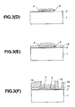
- FIGS. 3 (A)- 3 (H) are schematic cross sectional views, not to scale, that illustrate a method for fabricating the thermopile detector illustrated in FIG. 1 using the radiation absorbing composition illustrated in FIG. 2 .
- FIG. 4 is a schematic view that illustrates how to keep the radiation absorbing composition in a homogeneous state ready for a spin.
- FIG. 5 is a schematic cross sectional view in simplified and exaggerated form of another radiation-absorbing layer according to the present invention applied to the top surface of a thermocouple.
- FIG. 6 is a schematic cross sectional view in simplified and exaggerated form of still another absorbing layer according to the present invention applied to the top surface of a thermocouple.
- FIG. 7 is a schematic cross sectional view in simplified and exaggerated form of other radiation-absorbing layer according to the present invention applied to the top surface of a thermocouple.
- FIG. 1 is a schematic cross sectional view of a thermopile radiation detector incorporating a first exemplary embodiment of a radiation-absorbing layer 4 in accordance with the teaching of the invention.
- thermopile radiation detector is responsive to incident electromagnetic radiation having wavelengths of interest.
- thermopile detector is a thermopile infrared detector that is tuned to an infrared band of wavelengths.
- the thermopile detector includes a semiconductor substrate 1 having a cavity 5 formed beneath a thermocouple 3 backed by a membrane film 2 .
- the film 2 is formed with a process aperture 17 as entrance for etchant used to make the cavity 5 .
- Overlying the top of the thermocouple 3 is the radiation-absorbing layer 4 .
- the radiation-absorbing layer 4 includes a solid construction of a mixture of an oxide of silicon and particles.
- the particles include separate particles and/or linked particles of at least one material selected for absorbing incident radiation over wavelengths of interest.
- the solid construction includes a film of silicon dioxide (SiO 2 ) as a carrier for the particles of material selected for absorbing the incident radiation.
- R is about 0.017.
- the reflectance R may be expressed as 1.7%.
- Au gold
- the film of silicon dioxide is derived from a spin-on-glass (SOG) that is in a liquid state.
- SOG spin-on-glass
- the SOG used in embodiments was provided by and manufactured at Tokyo Ohka Kogyo Co., Ltd., Kanagawa, Japan.
- the SOG which does not contain any phosphoric component, such as phosphoric anhydride (P 2 O 5 ), was used, for a reason that will be explained later in connection with FIGS. 3 (F) and 3 (G).
- the gold (Au) is evaporated in a nitrogen atmosphere under a pressure of several hundreds Pa and collected.
- the evaporated substance collected which is black or dark brown, is very fragile. This fragile substance is stirred within a mill to obtain separate and/or linked particles of gold (Au).
- the particles of gold (Au) is put into the SOG and stirred well to provide a radiation-absorbing SOG composition 6 of the SOG and the gold (Au) incorporated in the SOG in the form of separate and/or linked particles.
- FIG. 2 schematically illustrates the SOG composition 6 within a container 32 . It is to be noted that the particles are not chemically bonded to the SOG.
- FIGS. 3 (A)- 3 (H) for illustrating a method of the present invention for fabricating a thermopile radiation detector as illustrated in FIG. 1 using the radiation absorbing SOG composition 6 illustrated in FIG. 2 .
- a single thermocouple is illustrated in these Figures, it should be realized that a large number of thermocouples could be simultaneously fabricated.
- a semiconductor substrate 1 is provided.
- phosphosilicate glass (PSG) is deposited to form a film 2 on the substrate 1 such that the film 2 overlies a surface of the substrate 1 .
- this film becomes a membrane, it is herein called a membrane film.
- thermopile detector fabricating processing a thermocouple 3 of the thermopile radiation detector is formed on the membrane film 2 .
- the SOG composition 6 is applied to form a film 7 of SOG composition such that the film 7 overlies the membrane film 2 and the thermocouple 3 .
- the process includes a spin and thermal bake step or steps at temperature 200° C.
- the particles of gold (Au) of the SOG composition 6 soon settle because specific weight of gold (Au) is heavy. This is not suitable for the spin.
- FIG. 4 illustrates how to keep the SOG composition 6 in a homogeneous state ready for the spin.
- the SOG composition (liquid) 6 contained in a helium (He) gas atmosphere within a container 11 .
- Helium gas enters via a pipe 33 onto the top surface of a body of the SOG composition 6 within the container 11 .
- an outlet pipe 34 Inserted deeply into the body of SOG composition 6 is an outlet pipe 34 .
- a required amount of the SOG composition 6 is supplied, as indicated by an arrow 13 , to a spin coater.
- an ultrasonic agitator 8 often called “homoginizer” or a stirring device 10 with a rotor 9 may be used.
- the container 6 is placed on the ultrasonic agitator 8 to continuously stir the SOG composition 6 .
- the rotor 9 within the body of SOG composition 6 is rotated to continuously Stir the SOG composition 6 .
- a first resist 14 having a first pattern is formed such that it overlies a portion of a surface of the film 2 of SOG composition.
- the film 2 of the SOG is etched to a desired pattern using a conventional wet etching technique.
- the first resist 14 is stripped or removed to expose the portion of the film 7 of SOG composition overlaid thereby as illustrated in FIG. 3 (D).
- removing unnecessary portion, by etching exposes the underlying membrane film 2 .
- SOG has a very high etch rate
- the unnecessary portion of the film 7 of the SOG composition is removed without any damage to the underlying membrane film 2 .
- the particles of gold (Au) flows out of the removed portion of the film 7 into the etchant liquid and settle on the substrate 1 .
- the substrate 1 is immersed into a mixture liquid containing iodine (I) or into aqua regia. In this manner, the desired shape of radiation-absorbing layer 4 is defined.
- a film 15 of PSG is formed such that the film 15 overlies the exposed membrane film 2 and the exposed portion of the film of SOG composition, which is the radiation-absorbing layer 4 .
- the thickness of the PSG film 15 is 1 ⁇ m.
- FIG. 3 (F) illustrating photolithograph.
- a second resist 16 is formed.
- the second resist 16 has a second pattern such that it overlies the film 15 of PSG except a portion above the top of the radiation-absorbing layer 4 , another portion used as a process aperture 17 (see FIG. 1 ), and other portions, not shown, for external connection.
- the film 15 of PSG and the underlying membrane film 2 are etched. Etching in this manner removes unnecessary portions to expose the top surface of the radiation-absorbing layer 4 , a portion of the substrate 1 for the process aperture 17 and other portions of the substrate 1 for external connection. In this etching, a so-called pad opening liquid is used.
- the pad opening liquid is a mixture of ammonia fluoride (NH 4 F), glacial acetic acid, and water.
- the SOG composition 6 that makes the radiation-absorbing layer 4 does not contain any phosphoric component, such as phosphoric anhydride (P 2 O 5 ) Due to the lack of such phosphoric component, the pad opening liquid does not dissolve the radiation-absorbing layer 4 .
- any phosphoric component such as phosphoric anhydride (P 2 O 5 ) Due to the lack of such phosphoric component, the pad opening liquid does not dissolve the radiation-absorbing layer 4 .
- heated hydrogen hydrate is used to etch the substrate 1 to remove a portion thereof to form a cavity 5 beneath the thermocouple 3 backed by the membrane film 2 .
- gold (Au) is used as a particle material.
- the present invention is not limited to the use of gold.
- the appropriate particle material can be selected from a group consisting of metals including gold (Au), carbon (C), and silicon (Si).
- the present invention is not limited to the use of particles of a single material selected from the group. A plurality of particle materials may be used. The selection of the material or materials of the particles and size(s) thereof determines optical, chemical, and mechanical properties of the radiation-absorbing layer.
- the step of forming the film 7 includes a sub-step of spinning the SOG composition 6 onto the membrane film 2 and the thermocouple 3 .
- the portion or portions of the SOG composition spun out of the membrane film 2 will adhere to a so-called cup provided around a spin table.
- the particles of gold (Au) can be recycled.
- the recycle includes a sub-step of collecting the portion of the SOG material spun out of the membrane film 2 and the thermocouple 3 and adhered to the cup around the spin table. This sub-step is followed by another sub-step of removing, by diluted hydrofluoric (HF) acid, oxide of silicon of the collected portion(s), adhered to the cup, to obtain the particles of gold (Au) for recycle.
- HF diluted hydrofluoric
- thermopile detectors Recycling of such precious material is advantageous in bringing down the cost of fabrication of thermopile detectors.
- the particles cannot be obtained for recycle if they are melted when in contact with the HF acid.
- the radiation-absorbing layer 4 is formed, using conventional semiconductor film patterning technique, by etching the film 7 of the SOG composition 6 . Any special processing technique deviated from the conventional semiconductor processing is not required for this etching. This adds to yield of the fabrication of the thermopile detectors.
- the radiation-absorbing layer 4 A comprise a solid construction that is a stack of five films.
- the stack of films includes a first film 18 derived from a radiation-absorbing SOG composition, which includes the SOG (the same SOG used in the previously described embodiment) containing the particles of gold (Au) in a first amount in terms of a first percent by volume. It also includes a second film 19 derived from a radiation-absorbing SOG composition, which includes the SOG containing the particles of gold (Au) in a second amount in terms of a second percent by volume.
- the second percent of the second film 19 is the highest among the first percent, second percent, third percent fourth percent and fifth percent.
- the second film 19 may be derived from a radiation-absorbing SOG composition, which includes the SOG containing the particles of gold (Au) in an amount in terms of a percent by volume that lies in a higher portion of a range from 10 to 90% by volume.
- the first percent of the first film 18 is sufficiently lower than the second percent to maintain mechanical strength and electrical insulation.
- the particles contained in the SOG are impurities.
- the mechanical strength of a film derived from the SOG composition depends on the amount of particles contained in the SOG. The less the amount of particles contained in the SOG is, the higher the mechanical strength of a film is. It is suggested by the inventors that there are cases where the mechanical strength of a film derived from a radiation-absorbing SOG composition drops if the amount of particles contained in the SOG is considerably large. It is also suggested by the inventors that there are cases where the electrical insulating property expected on a film derived from a radiation-absorbing SOG drops if the amount of the particles of gold (Au) is considerably large. To maintain mechanical strength and electrical insulation, the particles of gold (Au) in the first film 18 are sufficiently reduced in amount.
- the third percent, the fourth percent and the fifth percent drop in this order.
- This gradation in percent is intended to increase absorptance of the incident radiation by reducing reflection of incident radiation at the surface.
- the fifth film 22 is a skin or protector layer of the radiation-absorbing layer 4 A.
- the fifth percent may be zero.
- the fifth film 22 may be derived from the SOG containing no particles of gold (Au).
- the radiation-absorbing layer 4 B comprise a solid construction that is a stack of five films.
- the stack of films includes a first film 23 derived from a radiation-absorbing SOG composition, which includes the SOG (the same SOG used in the previously described embodiments) containing the particles of gold (Au) in a first amount in terms of a first percent 70% by volume. It also includes a second film 24 derived from a radiation-absorbing SOG composition, which includes the SOG containing the particles of silicon (Si) in a second amount in terms of a second percent 50% by volume.
- the second and fourth films 24 derived from the SOG composition containing the particles of silicon (Si) are superior in mechanical strength due to firm engagement of the particles in the SOG matrix. With these films 24 , the mechanical stress within the radiation-absorbing layer 4 B can be controlled.
- a radiation-absorbing SOG composition which includes the SOG containing the particles of silicon (Si) doped with a dopant selected from a group consisting of phosphorus (P), boron (B) and arsenic (As), may be used in forming the second and fourth films 24 .
- the fifth film 26 is a skin or protector layer of the radiation-absorbing layer 4 B.
- the fifth film 22 may be derived from the SOG containing no particles of gold (Au).
- the multi-layered construction shown in FIG. 6 makes it easy to provide a radiation-absorbing layer tuned to absorb incident radiation within a predetermined, e.g., infrared, band of wavelength and for reflecting incident radiation outside of the predetermined band of wavelength. This may be done by making appropriate selection, in the material and size, of the particles to be mixed with the SOG.
- a predetermined e.g., infrared
- FIG. 7 illustrating other radiation-absorbing layer 4 C according to the present invention applied to the top surface of a thermocouple 3 .
- the radiation-absorbing layer 4 C is substantially the same as the previously described radiation-absorbing layers 4 , 4 A and 4 B except underlying irregular topography ( 27 ) reflecting off incident radiation at different angles under the solid construction.
- the solid construction may be a single film as illustrated in FIG. 1 or a stack of films as illustrated in FIG. 5 or another stack of films as illustrated in FIG. 6 .
- the solid construction which is a stack of four films 28 , 29 , 30 and 31 , overlies the irregular topography formed above the top surface of the thermocouple via a dielectric (electrically insulating) film, not shown.
- thermocouple a dielectric film is formed on the top surface of the thermocouple.
- a film (1.5 ⁇ m thick) of aluminum (Al) oxide is formed on the dielectric film.
- protuberances 27 are formed, which provide the irregular topography.
- the material of the film is not limited to aluminum oxide. Silicon oxide doped with appropriate metal may be used. Using conventional semiconductor film forming techniques, a film (1.5 ⁇ m thick) of doped silicon oxide is formed on the dielectric film over the top surface of the thermocouple 3 . Subsequently, using photolithograph and dry etching techniques, protuberances 27 are formed, which provide the irregular topography.
- the doped silicon oxide is used to make the protuberances 27 , a portion of incident radiation is absorbed by the protuberances 27 , and the remainder is reflected off at different angles to be absorbed by the solid construction 28 , 29 , 30 and 31 .
- etching the film to leave a backing layer of about 0.5 ⁇ m thick in forming the protuberances 27 enhances the performance of irregular topography. The performance is increased because the backing layer reflects off incident radiation between the adjacent protuberances 27 .
- the solid construction is deeper at gaps between the protuberances 27 .
- the absorptance of a film is proportional to the film thickness.
- the increased thickness at the gaps is beneficial to enhancement of performance.
- the absorptance of the film is proportional to the percentage by volume of particles.
- the percentage by volume of the particles may be lowered if the increased thickness of the gaps is advantageously used without lowering the level of performance. The reduction in percentage by volume of the particles leads to easy work in film processing steps.
- the radiation-absorbing layers are formed using conventional semiconductor processing techniques including etching.
Abstract
A radiation-absorbing layer for a thermopile radiation detector highly absorbs incident radiation within a predetermined band of wavelengths. The layer comprises a solid construction of a mixture of an oxide of silicon and separate and/or linked particles of at least one material selected for absorbing incident radiation within the predetermined band.
Description
1. Field of the Invention
The present invention relates generally to radiation-absorbing layers for thermopile radiation detectors and methods for fabricating thermopile radiation detectors.
2. Description of the Background Art
A thermopile includes a plurality of thermocouples that are connected in series. Each thermocouple relies on the generation of the well-known Thompson and Peltier emfs that result from a temperature gradient across a junction between two dissimilar metals. A combination of the Thompson and Peltier effects produces the Seebeck emf, which is used in thermocouples.
In general, a thermopile radiation detector has a first set of junctions (hot junctions) that make good thermal contact with a radiation receiver (e.g., a black body) but which are electrically insulated from the radiation receiver. A second set of junctions (cold junctions) is attached to a support, which does not receive the radiation and which is therefore at a lower temperature. The incident radiation raises the temperature of the radiation receiver and produces a voltage output from the thermopile that is proportional to the energy absorbed. That is, the thermopile output voltage is proportional to a temperature difference and is, therefore, proportional to the total radiation energy received.
Thermopile infrared detectors are known, which have been constructed on electrically insulating thermally conducting membranes. This approach generally increases the electrical response of the thermopile. However, the increase in electrical response is made at the expense of special and complex “Back-end” processes such as backside etching with anisotropic etches.
Reference can be made to U.S. Pat. No. 3,405,271 (issued Oct. 8, 1968) entitled “Detector Having Radiation Collector Supported on Electrically Insulating Thermally Conducting Film” by N. B. Stevens et al., and also to U.S. Pat. No. 3,405,272 (issued Oct. 8, 1968) entitled “Film Supported Detector with Low Heat Transfer Impedance Path from Cold Junctions to Thermal Sink” by N. B. Stevens et al. In both of these U.S. patents, an aluminum oxide is disposed over surfaces of a cold sink and spans a cavity within the cold sink. The aluminum oxide film supports two thermoelectric materials (Bi and Sb).
A radiation-absorbing layer of blackening material is positioned locally within a small region that includes a thermocouple junction. The blackening material, such as gold (Au) black or bismuth (Bi) black, is evaporated on to the small region. In U.S. Pat. No. 3,405,272, a porous layer of bismuth (Bi) material is positioned over the surface of each collector. The blackening material renders the surface absorptive, thus increasing the electrical response (in volts output per watt of radiation received) of the thermopile.
As a radiation-absorbing layer for a thermopile infrared detector, gold (Au) is evaporated to grow dendrites on the thermocouple surface. A suggested method of growing dendrites of gold (Au) is to position the thermopile within a vacuum chamber so that it may be physically moved from the outside of the chamber. The majority of air is evacuated from the vacuum chamber down to a predetermined pressure. Subsequently, inertia gas is fed at a predetermined pressure to fill the vacuum chamber, keeping the system pressure within the chamber constant at a vacuum level falling in a range over several hundreds Pa. At such vacuum level, the mean free path within the vacuum chamber is extremely short. Gold material is positioned in an evaporation port directly below the thermocouple surface. The gold is heated and a gold smoke is produced which rises and engages the surface. Strict control of the evaporation rate is needed to allow dendrites to grow on the thermocouple surface.
The radiation-absorbing layer of dendrites of gold exhibits a high degree of absorptance exceeding 90%. However, one drawback to the use of dendrites of gold (Au) in thermopile detectors is a lack of a suitable patterning process that is compatible with standard integrated circuit processing techniques. Besides, the dendrites, which are unsuitable for conventional etching, require special care in a patterning process to remove unnecessary portions leaving the thermocouple surface.
As a radiation-absorbing layer for a thermopile infrared detector, a non-porous multi-layered construction is provided, which achieves a high degree of absorption by trapping radiation within a resonant cavity. This multi-layered radiation-absorbing layer can be formed by the standard integrated circuit processing techniques. However, one disadvantage of this conventional multi-layered construction is that its absorptance is about 70% and subject to variations with different wavelengths of the incident radiation. Total energy absorbed is therefore small. The use of this conventional approach is limited to the case where the electrical response (in volts output per watt of radiation received) of thermopile detectors is high.
An object of the present invention is to provide radiation-absorbing layers for thermopile radiation detectors, and methods for fabricating thermopile radiation detectors, that overcome the foregoing and other problems.
Another object of the present invention is a radiation-absorbing layer that is formed using conventional semiconductor processing techniques including photolithography and etching.
Another object of the present invention is to provide a radiation-absorbing layer that highly absorbs electromagnetic radiation within a desired band of wavelengths.
A further object of the present invention is to provide a radiation-absorbing layer that selectively absorbs electromagnetic radiation within an infrared band of wavelengths.
A still further object of the present invention is to provide a radiation-absorbing layer that absorbs electromagnetic radiation within a predetermined band of wavelengths and reflects electromagnetic radiation outside of the predetermined band of wavelengths.
According to one aspect of the present invention, there is provided a radiation-absorbing layer for a thermopile radiation detector that is responsive to incident radiation having wavelengths of interest, the radiation-absorbing layer comprising:
a solid construction of a mixture of an oxide of silicon and separate and/or linked particles of at least one material selected for absorbing incident radiation over the wavelengths of interest.
According to another aspect of the present invention, there is provided a radiation-absorbing layer for a thermopile radiation detector that is responsive to incident radiation having wavelengths of interest, the radiation-absorbing layer comprising:
a solid construction of a mixture of an oxide of silicon and separate and/or linked particles of at least one material selected for absorbing incident radiation within a predetermined band of wavelengths and for reflecting incident radiation outside of the predetermined band of wavelengths.
Further objects and advantages of the invention will be apparent from reading of the following description in conjunction with the accompanying drawings.
FIGS. 3(A)-3(H) are schematic cross sectional views, not to scale, that illustrate a method for fabricating the thermopile detector illustrated in FIG. 1 using the radiation absorbing composition illustrated in FIG. 2.
In general, the thermopile radiation detector is responsive to incident electromagnetic radiation having wavelengths of interest. In the embodiment, the thermopile detector is a thermopile infrared detector that is tuned to an infrared band of wavelengths.
The thermopile detector includes a semiconductor substrate 1 having a cavity 5 formed beneath a thermocouple 3 backed by a membrane film 2. The film 2 is formed with a process aperture 17 as entrance for etchant used to make the cavity 5. Overlying the top of the thermocouple 3 is the radiation-absorbing layer 4.
The radiation-absorbing layer 4 includes a solid construction of a mixture of an oxide of silicon and particles. The particles include separate particles and/or linked particles of at least one material selected for absorbing incident radiation over wavelengths of interest.
In the embodiment, the solid construction includes a film of silicon dioxide (SiO2) as a carrier for the particles of material selected for absorbing the incident radiation. The film of silicon dioxide has a refractive index (n) of about 1.3. Assuming that there is no absorption, a reflectance R at a surface of the film of silicon dioxide may be expressed as:
R=[(n−1)/(n+1)]2 (1).
R=[(n−1)/(n+1)]2 (1).
Putting n=1.3 into the equation (1), we obtain that R is about 0.017. Thus, the reflectance R may be expressed as 1.7%. This clearly indicates that almost all of incident radiation enters the film of silicon dioxide. In the embodiment, gold (Au), which is considered as a stable metal element, is used as a material of the particles incorporated in the film of silicon dioxide. The film of silicon dioxide is derived from a spin-on-glass (SOG) that is in a liquid state. The SOG used in embodiments was provided by and manufactured at Tokyo Ohka Kogyo Co., Ltd., Kanagawa, Japan. The SOG, which does not contain any phosphoric component, such as phosphoric anhydride (P2O5), was used, for a reason that will be explained later in connection with FIGS. 3(F) and 3(G).
The gold (Au) is evaporated in a nitrogen atmosphere under a pressure of several hundreds Pa and collected. The evaporated substance collected, which is black or dark brown, is very fragile. This fragile substance is stirred within a mill to obtain separate and/or linked particles of gold (Au). The particles of gold (Au) is put into the SOG and stirred well to provide a radiation-absorbing SOG composition 6 of the SOG and the gold (Au) incorporated in the SOG in the form of separate and/or linked particles. FIG. 2 schematically illustrates the SOG composition 6 within a container 32. It is to be noted that the particles are not chemically bonded to the SOG.
Reference is made to FIGS. 3(A)-3(H) for illustrating a method of the present invention for fabricating a thermopile radiation detector as illustrated in FIG. 1 using the radiation absorbing SOG composition 6 illustrated in FIG. 2. Although a single thermocouple is illustrated in these Figures, it should be realized that a large number of thermocouples could be simultaneously fabricated.
In FIG. 3(A), a semiconductor substrate 1 is provided. Using conventional semiconductor film forming processing, phosphosilicate glass (PSG) is deposited to form a film 2 on the substrate 1 such that the film 2 overlies a surface of the substrate 1. As this film becomes a membrane, it is herein called a membrane film. Using conventional thermopile detector fabricating processing, a thermocouple 3 of the thermopile radiation detector is formed on the membrane film 2.
In FIG. 3(B), using conventional semiconductor processing, the SOG composition 6 is applied to form a film 7 of SOG composition such that the film 7 overlies the membrane film 2 and the thermocouple 3. The process includes a spin and thermal bake step or steps at temperature 200° C. Turning back to FIG. 2 , the particles of gold (Au) of the SOG composition 6 soon settle because specific weight of gold (Au) is heavy. This is not suitable for the spin. FIG. 4 illustrates how to keep the SOG composition 6 in a homogeneous state ready for the spin. In FIG. 4 , the SOG composition (liquid) 6 contained in a helium (He) gas atmosphere within a container 11. Helium gas, as indicated by an arrow 12, enters via a pipe 33 onto the top surface of a body of the SOG composition 6 within the container 11. Inserted deeply into the body of SOG composition 6 is an outlet pipe 34. Via this pipe 34, a required amount of the SOG composition 6 is supplied, as indicated by an arrow 13, to a spin coater. To keep the SOG composition 6 in a homogeneous state ready for the spin, an ultrasonic agitator 8 often called “homoginizer” or a stirring device 10 with a rotor 9 may be used. The container 6 is placed on the ultrasonic agitator 8 to continuously stir the SOG composition 6. Alternatively, the rotor 9 within the body of SOG composition 6 is rotated to continuously Stir the SOG composition 6.
Turning back to FIG. 3(C) for illustrating photolithography, a first resist 14 having a first pattern is formed such that it overlies a portion of a surface of the film 2 of SOG composition. Using the first resist 14 as a mask, the film 2 of the SOG is etched to a desired pattern using a conventional wet etching technique. The first resist 14 is stripped or removed to expose the portion of the film 7 of SOG composition overlaid thereby as illustrated in FIG. 3(D).
In FIG. 3(D), removing unnecessary portion, by etching, exposes the underlying membrane film 2. As SOG has a very high etch rate, the unnecessary portion of the film 7 of the SOG composition is removed without any damage to the underlying membrane film 2. The particles of gold (Au) flows out of the removed portion of the film 7 into the etchant liquid and settle on the substrate 1. To remove the settled particles of gold (Au), the substrate 1 is immersed into a mixture liquid containing iodine (I) or into aqua regia. In this manner, the desired shape of radiation-absorbing layer 4 is defined.
In FIG. 3(E), a film 15 of PSG is formed such that the film 15 overlies the exposed membrane film 2 and the exposed portion of the film of SOG composition, which is the radiation-absorbing layer 4. The thickness of the PSG film 15 is 1 μm.
Reference is made to FIG. 3(F) illustrating photolithograph. In FIG. 3(F), a second resist 16 is formed. The second resist 16 has a second pattern such that it overlies the film 15 of PSG except a portion above the top of the radiation-absorbing layer 4, another portion used as a process aperture 17 (see FIG. 1), and other portions, not shown, for external connection.
Referring also to FIG. 3(G), using the second resist 16 as a mask, the film 15 of PSG and the underlying membrane film 2 are etched. Etching in this manner removes unnecessary portions to expose the top surface of the radiation-absorbing layer 4, a portion of the substrate 1 for the process aperture 17 and other portions of the substrate 1 for external connection. In this etching, a so-called pad opening liquid is used. The pad opening liquid is a mixture of ammonia fluoride (NH4F), glacial acetic acid, and water. As mentioned before, the SOG composition 6 that makes the radiation-absorbing layer 4 does not contain any phosphoric component, such as phosphoric anhydride (P2O5) Due to the lack of such phosphoric component, the pad opening liquid does not dissolve the radiation-absorbing layer 4.
In FIG. 3(H), with the film 15 of PSG as a mask, heated hydrogen hydrate is used to etch the substrate 1 to remove a portion thereof to form a cavity 5 beneath the thermocouple 3 backed by the membrane film 2.
In the embodiment, gold (Au) is used as a particle material. The present invention is not limited to the use of gold. The appropriate particle material can be selected from a group consisting of metals including gold (Au), carbon (C), and silicon (Si). The present invention is not limited to the use of particles of a single material selected from the group. A plurality of particle materials may be used. The selection of the material or materials of the particles and size(s) thereof determines optical, chemical, and mechanical properties of the radiation-absorbing layer.
Turning back to FIG. 3(B), the step of forming the film 7 includes a sub-step of spinning the SOG composition 6 onto the membrane film 2 and the thermocouple 3. The portion or portions of the SOG composition spun out of the membrane film 2 will adhere to a so-called cup provided around a spin table. The particles of gold (Au) can be recycled. The recycle includes a sub-step of collecting the portion of the SOG material spun out of the membrane film 2 and the thermocouple 3 and adhered to the cup around the spin table. This sub-step is followed by another sub-step of removing, by diluted hydrofluoric (HF) acid, oxide of silicon of the collected portion(s), adhered to the cup, to obtain the particles of gold (Au) for recycle.
Recycling of such precious material is advantageous in bringing down the cost of fabrication of thermopile detectors.
However, the particles cannot be obtained for recycle if they are melted when in contact with the HF acid.
From the preceding description of the embodiment, it is now appreciated that the radiation-absorbing layer 4 is formed, using conventional semiconductor film patterning technique, by etching the film 7 of the SOG composition 6. Any special processing technique deviated from the conventional semiconductor processing is not required for this etching. This adds to yield of the fabrication of the thermopile detectors.
Reference is now made to FIG. 5 illustrating another radiation-absorbing layer 4A according to the present invention applied to the top surface of a thermocouple 3. The radiation-absorbing layer 4A comprise a solid construction that is a stack of five films. The stack of films includes a first film 18 derived from a radiation-absorbing SOG composition, which includes the SOG (the same SOG used in the previously described embodiment) containing the particles of gold (Au) in a first amount in terms of a first percent by volume. It also includes a second film 19 derived from a radiation-absorbing SOG composition, which includes the SOG containing the particles of gold (Au) in a second amount in terms of a second percent by volume. It further includes a third film 20 derived from a radiation-absorbing SOG composition, which includes the SOG containing the particles of gold (Au) in a third amount in terms of a third percent by volume. It still further includes a fourth film 21 derived a radiation-absorbing SOG composition, which includes the SOG containing the particles of gold (Au) in a fourth amount in terms of a fourth percent by volume. It finally includes a fifth film 22 derived from a radiation-absorbing SOG composition, which includes the SOG containing the particles of gold (Au) in a fifth amount in terms of a fifth percent by volume. As shown in FIG. 5 , the fifth film 22, fourth film 21, third film 20, second film 19 and first film 18 overlie one after another.
The second percent of the second film 19 is the highest among the first percent, second percent, third percent fourth percent and fifth percent.
With regard to the particles of gold (Au) in amount in a film, the more the amount of particles contained in the SOG, the higher the radiation-absorbing performance is. In this multi-layered construction, the second film 19 may be derived from a radiation-absorbing SOG composition, which includes the SOG containing the particles of gold (Au) in an amount in terms of a percent by volume that lies in a higher portion of a range from 10 to 90% by volume.
The first percent of the first film 18 is sufficiently lower than the second percent to maintain mechanical strength and electrical insulation.
In each SOG composition, the particles contained in the SOG are impurities. The mechanical strength of a film derived from the SOG composition depends on the amount of particles contained in the SOG. The less the amount of particles contained in the SOG is, the higher the mechanical strength of a film is. It is suggested by the inventors that there are cases where the mechanical strength of a film derived from a radiation-absorbing SOG composition drops if the amount of particles contained in the SOG is considerably large. It is also suggested by the inventors that there are cases where the electrical insulating property expected on a film derived from a radiation-absorbing SOG drops if the amount of the particles of gold (Au) is considerably large. To maintain mechanical strength and electrical insulation, the particles of gold (Au) in the first film 18 are sufficiently reduced in amount.
The third percent, the fourth percent and the fifth percent drop in this order. This gradation in percent is intended to increase absorptance of the incident radiation by reducing reflection of incident radiation at the surface. The fifth film 22 is a skin or protector layer of the radiation-absorbing layer 4A. Thus, the fifth percent may be zero. In other words, the fifth film 22 may be derived from the SOG containing no particles of gold (Au).
From the preceding description with reference to FIG. 5 , it is appreciated, as an advantage, that the multi-layered construction of the radiation-absorbing layer 4A makes it easy to design the optical and mechanical property.
Reference is next made to FIG. 6 illustrating still another radiation-absorbing layer 4B according to the present invention applied to the top surface of a thermocouple 3. The radiation-absorbing layer 4B comprise a solid construction that is a stack of five films. The stack of films includes a first film 23 derived from a radiation-absorbing SOG composition, which includes the SOG (the same SOG used in the previously described embodiments) containing the particles of gold (Au) in a first amount in terms of a first percent 70% by volume. It also includes a second film 24 derived from a radiation-absorbing SOG composition, which includes the SOG containing the particles of silicon (Si) in a second amount in terms of a second percent 50% by volume. It further includes a third film 25 derived from a radiation-absorbing SOG composition, which includes the SOG containing the particles of gold (Au) in a third amount in terms of a third percent by volume. It still further includes a fourth film 24 derived the same radiation-absorbing SOG composition, which includes the SOG containing the particles of gold (Si) in the second amount in terms of second percent 50% by volume. It finally includes a fifth film 26 derived from a radiation-absorbing SOG composition, which includes the SOG containing the particles of gold (Au) in a fourth amount in terms of a fourth percent 10% by volume. As shown in FIG. 6 , the fifth film 26, fourth film 24, third film 25, second film 24 and first film 23 overlie one after another.
The second and fourth films 24 derived from the SOG composition containing the particles of silicon (Si) are superior in mechanical strength due to firm engagement of the particles in the SOG matrix. With these films 24, the mechanical stress within the radiation-absorbing layer 4B can be controlled. To meet a need to accomplish increased absorption of incident rays having wavelengths within an infrared band, a radiation-absorbing SOG composition, which includes the SOG containing the particles of silicon (Si) doped with a dopant selected from a group consisting of phosphorus (P), boron (B) and arsenic (As), may be used in forming the second and fourth films 24.
The fifth film 26 is a skin or protector layer of the radiation-absorbing layer 4B. Thus, the fifth film 22 may be derived from the SOG containing no particles of gold (Au).
From the preceding description, it is appreciated, as an advantage, that the multi-layered construction shown in FIG. 6 makes it easy to provide a radiation-absorbing layer tuned to absorb incident radiation within a predetermined, e.g., infrared, band of wavelength and for reflecting incident radiation outside of the predetermined band of wavelength. This may be done by making appropriate selection, in the material and size, of the particles to be mixed with the SOG.
Reference is finally made to FIG. 7 illustrating other radiation-absorbing layer 4C according to the present invention applied to the top surface of a thermocouple 3. The radiation-absorbing layer 4C is substantially the same as the previously described radiation-absorbing layers 4, 4A and 4B except underlying irregular topography (27) reflecting off incident radiation at different angles under the solid construction. The solid construction may be a single film as illustrated in FIG. 1 or a stack of films as illustrated in FIG. 5 or another stack of films as illustrated in FIG. 6. In FIG. 7 , the solid construction, which is a stack of four films 28, 29, 30 and 31, overlies the irregular topography formed above the top surface of the thermocouple via a dielectric (electrically insulating) film, not shown.
The manner of forming the irregular topography will be explained.
First, a dielectric film is formed on the top surface of the thermocouple. Next, a film (1.5 μm thick) of aluminum (Al) oxide is formed on the dielectric film. Subsequently, using photolithograph and dry etching techniques, protuberances 27 are formed, which provide the irregular topography.
The material of the film is not limited to aluminum oxide. Silicon oxide doped with appropriate metal may be used. Using conventional semiconductor film forming techniques, a film (1.5 μm thick) of doped silicon oxide is formed on the dielectric film over the top surface of the thermocouple 3. Subsequently, using photolithograph and dry etching techniques, protuberances 27 are formed, which provide the irregular topography.
In the case where the aluminum oxide is used to make the protuberances 27, almost all of incident radiation is reflected off at different angles to be absorbed by the solid construction 28, 29, 30 and 31.
In the case where the doped silicon oxide is used to make the protuberances 27, a portion of incident radiation is absorbed by the protuberances 27, and the remainder is reflected off at different angles to be absorbed by the solid construction 28, 29, 30 and 31.
In the case where the aluminum oxide is used to form a film (1.5 μm thick), etching the film to leave a backing layer of about 0.5 μm thick in forming the protuberances 27 enhances the performance of irregular topography. The performance is increased because the backing layer reflects off incident radiation between the adjacent protuberances 27.
Subsequently after the formation of the protuberances 27, gaps or spaces between the protuberances are filled with the SOG composition(s) containing the particles or gold (Au) or silicon (Si). As shown in FIG. 7 , the solid construction is deeper at gaps between the protuberances 27. With the same percentage by volume of particles, the absorptance of a film is proportional to the film thickness. Thus, the increased thickness at the gaps is beneficial to enhancement of performance. With the same thickness of a film, the absorptance of the film is proportional to the percentage by volume of particles. Thus, the percentage by volume of the particles may be lowered if the increased thickness of the gaps is advantageously used without lowering the level of performance. The reduction in percentage by volume of the particles leads to easy work in film processing steps.
From the preceding description of various implementations of the present invention, it is understood as an advantage that the radiation-absorbing layers are formed using conventional semiconductor processing techniques including etching.
While the present invention has been particularly described, in conjunction with exemplary embodiments, it is evident that many alternatives, modifications and variations will be apparent to those skilled in the art in light of the foregoing description. It is therefore contemplated that the appended claims will embrace any such alternatives, modifications and variations as falling within the true scope and spirit of the present invention.
This application claims the priority of Japanese Patent Applications No. P2001-286477, filed Sep. 20, 2001, the disclosure of which is hereby incorporated by reference in its entirety.
Claims (21)
1. In a thermopile radiation detector that is responsive to incident radiation having wavelengths of an infrared band, including:
a semiconductor substrate;
a membrane film formed on the semiconductor substrate;
a thermocouple backed by the membrane film;
the semiconductor substrate having a cavity formed beneath the thermocouple; and
a radiation-absorbing layer overlying the thermocouple, the radiation-absorbing layer comprising:
a solid construction of a mixture of an oxide of silicon and separate and/or linked particles of at least one material selected for absorbing incident radiation over the wavelengths of the infrared-band.
2. The radiation-absorbing layer as claimed in claim 1 , wherein the material has a higher absorptance than the oxide of silicon does over the wavelengths of the infrared band; and wherein the solid construction has a higher absorptance than the oxide of silicon does over the wavelengths of the infrared band.
3. The radiation-absorbing layer as claimed in claim 2 , wherein the solid construction incorporates separate and/or linked particles of a material that has a higher reflectance than the oxide of silicon does over the wavelengths of the infrared band.
4. The radiation-absorbing layer as claimed in claim 3 , wherein the solid construction is derived from a spin-on-glass (SOG) containing the particles.
5. The radiation-absorbing layer as claimed in claim 1 , wherein the solid construction is derived from a spin-on-glass (SOG) containing the particles.
6. The radiation-absorbing layer as claimed in claim 5 , wherein the solid construction is a stack of a plurality of films including a first film derived from the SOG containing the particles in a first amount and a second film derived from the SOG containing the particles in a second amount that differs from the first amount.
7. The radiation-absorbing layer as claimed in claim 5 , wherein the solid construction is a stack of a plurality of films including a first film derived from the SOG containing the particles of a first material in a first amount and a second film derived from the SOG containing the particles of a second material that differs from the first material in a second amount that differs from the first amount.
8. The radiation-absorbing layer as claimed in claim 5 , wherein the SOG does not contain any phosphoric component.
9. The radiation-absorbing layer as claimed in claim 5 , wherein the material is selected from a group consisting of metals including gold (Au), carbon (C) and silicon (Si).
10. The radiation-absorbing layer as claimed in claim 5 , further comprising irregular topography reflecting off incident radiation at different angles, and wherein the solid construction overlies the irregular topography.
11. The radiation-absorbing layer as claimed in claim 10 , wherein the irregular topography includes protuberances.
12. The radiation-absorbing layer as claimed in claim 11 , wherein the solid construction is a stack of a plurality of films including first, second, third and fourth films each being derived from the SOG containing the particles.
13. The radiation-absorbing layer as claimed in claim 5 , wherein the solid construction is a film derived from the SOG containing the particles of gold (Au) in an amount ranging from 10 to 90% by volume.
14. The radiation-absorbing layer as claimed in claim 5 , wherein the solid construction is a stack of a plurality of films including a first film derived from the SOG containing the particles of gold (Au) in a first amount in terms of first percent by volume, a second film derived from the SOG containing the particles of gold (Au) in a second amount in terms of second percent by volume, a third film derived from the SOG containing the particles of gold (Au) in a third amount in terms of third percent by volume, a fourth film derived from the SOG containing the particles of gold (Au) in a fourth amount in terms of fourth percent by volume and a fifth film derived from the SOG containing the particles of gold (Au) in a fifth amount in terms of fifth percent by volume; and wherein the fifth film, fourth film, third film, second film and first film overlie one after another; and wherein the second percent is the highest among the first percent, second percent, third percent fourth percent and fifth percent; and wherein the first percent is sufficiently lower than the second percent to maintain mechanical strength and electrical insulation of the first film, and where the third percent, the fourth percent and the fifth percent drop in this order.
15. The radiation-absorbing layer as claimed in claim 5 , wherein the solid construction is a stack of a plurality of films including a first film derived from the SOG containing the particles of gold (Au) in a first amount of 70% by volume, a second film derived from the SOG containing the particles of silicon (Si) in a second amount, a third film derived from the SOG containing the particles of gold (Au) in a third amount, a fourth film derived from the SOG containing the particles of silicon (Si) in a fourth amount and a fifth film derived from the SOG containing the particles of gold (Au) in a fifth amount of 10% by volume, and wherein the fifth film, fourth film, third film, second film and first film overlie one after another.
16. The radiation-absorbing layer as claimed in claim 5 , wherein the oxide of silicon has a refractive index of about 1.3 and a reflectance of about 1.7% at a surface thereof assuming that there is no absorption of incident radiation.
17. The radiation-absorbing layer as claimed in claim 5 , wherein the material is selected from one of gold (Au) and silicon (Si) doped with a dopant selected from a group consisting of phosphorus (P), boron (B) and arsenic (As).
18. A thermopile infrared radiation detector that is responsive to incident radiation having wavelengths of an infrared band, comprising:
a semiconductor substrate;
a membrane film formed on the semiconductor substrate;
a thermocouple backed by the membrane film;
the semiconductor substrate having a cavity formed beneath the thermocouple; and
a radiation-absorbing layer overlying the thermocouple, the radiation-absorbing layer including:
a solid construction of a mixture of an oxide of silicon and separate and/or linked particles of at least one material selected for absorbing incident radiation within the infrared band of wavelengths and for reflecting incident radiation outside of the infrared band of wavelengths.
19. A radiation-absorbing layer for a thermopile radiation detector that is responsive to incident radiation having wavelengths of interest, the radiation-absorbing layer comprising:
a solid construction of a mixture of an oxide of silicon and separate and/or linked particles of at least one material selected for absorbing incident radiation over the wavelengths of interest,
the solid construction being derived from a spin-on-glass (SOG) containing the particles,
wherein the solid construction is a stack of a plurality of films including a first film derived from the SOG containing the particles of gold (Au) in a first amount in terms of first percent by volume, a second film derived from the SOG containing the particles of gold (Au) in a second amount in terms of second percent by volume, a third film derived from the SOG containing the particles of gold (Au) in a third amount in terms of third percent by volume, a fourth film derived from the SOG containing the particles of gold (Au) in a fourth amount in terms of fourth percent by volume and a fifth film derived from the SOG containing the particles of gold (Au) in a fifth amount in terms of fifth percent by volume; and
wherein the fifth film, fourth film, third film, second film and first film overlie one after another; and
wherein the second percent is the highest among the first percent, second percent, third percent fourth percent and fifth percent; and
wherein the first percent is sufficiently lower than the second percent to maintain mechanical strength and electrical insulation of the first film, and
wherein the third percent, the fourth percent and the fifth percent drop in this order.
20. A radiation-absorbing layer for a thermopile radiation detector that is responsive to incident radiation having wavelengths of interest, the radiation-absorbing layer comprising:
a solid construction of a mixture of an oxide of silicon and separate and/or linked particles of at least one material selected for absorbing incident radiation over the wavelengths of interest,
the solid construction being derived from a spin-on-glass (SOG) containing the particles,
wherein the solid construction is a stack of a plurality of films including a first film derived from the SOG containing the particles of gold (Au) in a first amount of 70% by volume, a second film derived from the SOG containing the particles of silicon (Si) in a second amount, a third film derived from the SOG containing the particles of gold (Au) in a third amount, a fourth film derived from the SOG containing the particles of silicon (Si) in a fourth amount and a fifth film derived from the SOG containing the particles of gold (Au) in a fifth amount of 10% by volume, and
wherein the fifth film, fourth film, third film, second film and first film overlie one after another.
21. A radiation-absorbing layer for a thermopile radiation detector that is responsive to incident radiation having wavelengths of interest, the radiation-absorbing layer comprising:
a solid construction of a mixture of an oxide of silicon and separate and/or linked particles of at least one material selected for absorbing incident radiation over the wavelengths of interest,
the solid construction being derived from a spin-on-glass (SOG) containing the particles, and
irregular topography reflecting off incident radiation at different angles, and
wherein the solid construction overlies the irregular topography, and
wherein the irregular topography includes protuberances, and
wherein the solid construction is a stack of a plurality of films including first, second, third and fourth films, each being derived from the SOG containing the particles.
Applications Claiming Priority (2)
| Application Number | Priority Date | Filing Date | Title |
|---|---|---|---|
| JP2001-286477 | 2001-09-20 | ||
| JP2001286477A JP4144204B2 (en) | 2001-09-20 | 2001-09-20 | Light absorbing film and manufacturing method thereof |
Publications (2)
| Publication Number | Publication Date |
|---|---|
| US20030054179A1 US20030054179A1 (en) | 2003-03-20 |
| US6949286B2 true US6949286B2 (en) | 2005-09-27 |
Family
ID=19109450
Family Applications (1)
| Application Number | Title | Priority Date | Filing Date |
|---|---|---|---|
| US10/245,687 Expired - Fee Related US6949286B2 (en) | 2001-09-20 | 2002-09-18 | Radiation-absorbing layers for thermopile radiation detectors |
Country Status (2)
| Country | Link |
|---|---|
| US (1) | US6949286B2 (en) |
| JP (1) | JP4144204B2 (en) |
Cited By (9)
| Publication number | Priority date | Publication date | Assignee | Title |
|---|---|---|---|---|
| US20050017175A1 (en) * | 2003-07-24 | 2005-01-27 | Delphi Technologies, Inc. | Infrared sensor package |
| US20070297485A1 (en) * | 2004-06-09 | 2007-12-27 | Perkinelmer Optoelectronics Gmbh & Co. Kg | Sensor Element |
| US7726876B2 (en) | 2007-03-14 | 2010-06-01 | Entegris, Inc. | System and method for non-intrusive thermal monitor |
| US20110180711A1 (en) * | 2010-01-26 | 2011-07-28 | Seiko Epson Corporation | Thermal detector, thermal detection device and electronic instrument, and method for manufacturing thermal detector |
| US20110235676A1 (en) * | 2010-03-26 | 2011-09-29 | Seiko Epson Corporation | Thermal detector, thermal detection device, and electronic instrument |
| US8158943B2 (en) | 2009-04-12 | 2012-04-17 | Ud Holdings, Llc | Infrared detector |
| US20120161004A1 (en) * | 2010-12-22 | 2012-06-28 | Seiko Epson Corporation | Thermal detector, thermal detection device, electronic instrument, and thermal detector manufacturing method |
| US8395118B2 (en) | 2009-04-12 | 2013-03-12 | Ud Holdings, Llc | Infrared detector having at least one switch for modulation and/or bypass |
| US20140036953A1 (en) * | 2010-04-26 | 2014-02-06 | Hme Co., Ltd. | Temperature sensor device and radiation thermometer using this device, production method of temperature sensor device, multi-layered thin film thermopile using photo-resist film and radiation thermometer using this thermopile, and production method of multi-layered thin film thermopile |
Families Citing this family (4)
| Publication number | Priority date | Publication date | Assignee | Title |
|---|---|---|---|---|
| DE102010042108B4 (en) | 2010-01-18 | 2013-10-17 | Heimann Sensor Gmbh | Thermopile infrared sensor in monolithic Si micromechanics |
| CN104246457B (en) | 2012-02-16 | 2018-07-20 | 赫曼传感器公司 | Thermopile infrared sensor structure with high fill level |
| WO2014199583A1 (en) * | 2013-06-10 | 2014-12-18 | パナソニックIpマネジメント株式会社 | Infrared sensor |
| CN113091919A (en) * | 2021-04-12 | 2021-07-09 | 上海芯物科技有限公司 | Thermopile sensor and manufacturing method thereof |
Citations (15)
| Publication number | Priority date | Publication date | Assignee | Title |
|---|---|---|---|---|
| US3405271A (en) | 1966-05-02 | 1968-10-08 | Santa Barbara Res Ct | Detector having radiation collector supported on electrically insulating thermally conducting film |
| US3405272A (en) | 1966-05-02 | 1968-10-08 | Santa Barbara Res Ct | Film supported detector with low heat transfer impedance path from cold junctions tothermal sink |
| US4111717A (en) * | 1977-06-29 | 1978-09-05 | Leeds & Northrup Company | Small-size high-performance radiation thermopile |
| US4282290A (en) | 1980-01-23 | 1981-08-04 | The United States Of America As Represented By The Secretary Of The Air Force | High absorption coating |
| US5316854A (en) * | 1991-12-06 | 1994-05-31 | Ppg Industries, Inc. | Glass or quartz articles having high temperature UV absorbing coatings containing ceria |
| US5412279A (en) * | 1991-09-19 | 1995-05-02 | U.S. Philips Corporation | Antistatic coating for, in particular, a cathode ray tube comprising latex particles of a polypyrole compound in a silicon dioxide matrix |
| US5545897A (en) * | 1994-10-04 | 1996-08-13 | Santa Barbara Research Center | Optically-based chemical detection system |
| US5689087A (en) | 1994-10-04 | 1997-11-18 | Santa Barbara Research Center | Integrated thermopile sensor for automotive, spectroscopic and imaging applications, and methods of fabricating same |
| US5982014A (en) * | 1997-05-30 | 1999-11-09 | Thermalytics, Inc. | Microfabricated silicon thermopile sensor |
| US6060151A (en) * | 1995-04-06 | 2000-05-09 | Ohashi & Associates | Glass sheet covered with colored film |
| US6222111B1 (en) * | 1995-06-07 | 2001-04-24 | Raytheon Company | Spectrally selective thermopile detector |
| US20020018887A1 (en) * | 2000-08-14 | 2002-02-14 | Takao Sumida | Light absorption/anti-reflection material member and display apparatus |
| US20020025425A1 (en) * | 1999-10-25 | 2002-02-28 | Mitsuhiro Kawazu | Light absorbing pattern film coated article production method and light absorbing pattern film coated articles |
| US6368400B1 (en) | 2000-07-17 | 2002-04-09 | Honeywell International | Absorbing compounds for spin-on-glass anti-reflective coatings for photolithography |
| US20020162585A1 (en) * | 2001-02-28 | 2002-11-07 | Shin Sugawara | Photoelectric conversion device and method of manufacturing the same |
-
2001
- 2001-09-20 JP JP2001286477A patent/JP4144204B2/en not_active Expired - Fee Related
-
2002
- 2002-09-18 US US10/245,687 patent/US6949286B2/en not_active Expired - Fee Related
Patent Citations (15)
| Publication number | Priority date | Publication date | Assignee | Title |
|---|---|---|---|---|
| US3405271A (en) | 1966-05-02 | 1968-10-08 | Santa Barbara Res Ct | Detector having radiation collector supported on electrically insulating thermally conducting film |
| US3405272A (en) | 1966-05-02 | 1968-10-08 | Santa Barbara Res Ct | Film supported detector with low heat transfer impedance path from cold junctions tothermal sink |
| US4111717A (en) * | 1977-06-29 | 1978-09-05 | Leeds & Northrup Company | Small-size high-performance radiation thermopile |
| US4282290A (en) | 1980-01-23 | 1981-08-04 | The United States Of America As Represented By The Secretary Of The Air Force | High absorption coating |
| US5412279A (en) * | 1991-09-19 | 1995-05-02 | U.S. Philips Corporation | Antistatic coating for, in particular, a cathode ray tube comprising latex particles of a polypyrole compound in a silicon dioxide matrix |
| US5316854A (en) * | 1991-12-06 | 1994-05-31 | Ppg Industries, Inc. | Glass or quartz articles having high temperature UV absorbing coatings containing ceria |
| US5545897A (en) * | 1994-10-04 | 1996-08-13 | Santa Barbara Research Center | Optically-based chemical detection system |
| US5689087A (en) | 1994-10-04 | 1997-11-18 | Santa Barbara Research Center | Integrated thermopile sensor for automotive, spectroscopic and imaging applications, and methods of fabricating same |
| US6060151A (en) * | 1995-04-06 | 2000-05-09 | Ohashi & Associates | Glass sheet covered with colored film |
| US6222111B1 (en) * | 1995-06-07 | 2001-04-24 | Raytheon Company | Spectrally selective thermopile detector |
| US5982014A (en) * | 1997-05-30 | 1999-11-09 | Thermalytics, Inc. | Microfabricated silicon thermopile sensor |
| US20020025425A1 (en) * | 1999-10-25 | 2002-02-28 | Mitsuhiro Kawazu | Light absorbing pattern film coated article production method and light absorbing pattern film coated articles |
| US6368400B1 (en) | 2000-07-17 | 2002-04-09 | Honeywell International | Absorbing compounds for spin-on-glass anti-reflective coatings for photolithography |
| US20020018887A1 (en) * | 2000-08-14 | 2002-02-14 | Takao Sumida | Light absorption/anti-reflection material member and display apparatus |
| US20020162585A1 (en) * | 2001-02-28 | 2002-11-07 | Shin Sugawara | Photoelectric conversion device and method of manufacturing the same |
Cited By (16)
| Publication number | Priority date | Publication date | Assignee | Title |
|---|---|---|---|---|
| US7180064B2 (en) * | 2003-07-24 | 2007-02-20 | Delphi Technologies, Inc. | Infrared sensor package |
| US20050017175A1 (en) * | 2003-07-24 | 2005-01-27 | Delphi Technologies, Inc. | Infrared sensor package |
| US8215831B2 (en) * | 2004-06-09 | 2012-07-10 | Excelitas Technologies Gmbh & Co. Kg | Sensor element |
| US20070297485A1 (en) * | 2004-06-09 | 2007-12-27 | Perkinelmer Optoelectronics Gmbh & Co. Kg | Sensor Element |
| US7726876B2 (en) | 2007-03-14 | 2010-06-01 | Entegris, Inc. | System and method for non-intrusive thermal monitor |
| US9151676B2 (en) | 2009-04-12 | 2015-10-06 | Ud Holdings, Llc | Infrared detector having at least one switch for modulation and/or bypass |
| US8158943B2 (en) | 2009-04-12 | 2012-04-17 | Ud Holdings, Llc | Infrared detector |
| US8395118B2 (en) | 2009-04-12 | 2013-03-12 | Ud Holdings, Llc | Infrared detector having at least one switch for modulation and/or bypass |
| US20110180711A1 (en) * | 2010-01-26 | 2011-07-28 | Seiko Epson Corporation | Thermal detector, thermal detection device and electronic instrument, and method for manufacturing thermal detector |
| US9000372B2 (en) * | 2010-01-26 | 2015-04-07 | Seiko Epson Corporation | Thermal detector, thermal detection device and electronic instrument, and method for manufacturing thermal detector |
| US20110235676A1 (en) * | 2010-03-26 | 2011-09-29 | Seiko Epson Corporation | Thermal detector, thermal detection device, and electronic instrument |
| US9182288B2 (en) * | 2010-03-26 | 2015-11-10 | Seiko Epson Corporation | Thermal detector, thermal detection device, and electronic instrument |
| US20140036953A1 (en) * | 2010-04-26 | 2014-02-06 | Hme Co., Ltd. | Temperature sensor device and radiation thermometer using this device, production method of temperature sensor device, multi-layered thin film thermopile using photo-resist film and radiation thermometer using this thermopile, and production method of multi-layered thin film thermopile |
| US9759613B2 (en) * | 2010-04-26 | 2017-09-12 | Hme Co., Ltd. | Temperature sensor device and radiation thermometer using this device, production method of temperature sensor device, multi-layered thin film thermopile using photo-resist film and radiation thermometer using this thermopile, and production method of multi-layered thin film thermopile |
| US20120161004A1 (en) * | 2010-12-22 | 2012-06-28 | Seiko Epson Corporation | Thermal detector, thermal detection device, electronic instrument, and thermal detector manufacturing method |
| US8941063B2 (en) * | 2010-12-22 | 2015-01-27 | Seiko Epson Corporation | Thermal detector, thermal detection device, electronic instrument, and thermal detector manufacturing method |
Also Published As
| Publication number | Publication date |
|---|---|
| JP4144204B2 (en) | 2008-09-03 |
| US20030054179A1 (en) | 2003-03-20 |
| JP2003098338A (en) | 2003-04-03 |
Similar Documents
| Publication | Publication Date | Title |
|---|---|---|
| JP3112680B2 (en) | Semiconductor film bolometer thermal infrared detector | |
| US6949286B2 (en) | Radiation-absorbing layers for thermopile radiation detectors | |
| JP3386830B2 (en) | Bolometer, method for forming bolometer cell on semiconductor substrate, and infrared detection array comprising bolometer array | |
| EP1198835B1 (en) | Dual wafer attachment process | |
| CA2190077C (en) | Suspended microstructures | |
| EP0534768B1 (en) | Uncooled infrared detector and method for forming the same | |
| US4782028A (en) | Process methodology for two-sided fabrication of devices on thinned silicon | |
| US6198098B1 (en) | Microstructure for infrared detector and method of making same | |
| US6498073B2 (en) | Back illuminated imager with enhanced UV to near IR sensitivity | |
| US5939971A (en) | Infrared bolometer | |
| US4131985A (en) | Thin silicon devices | |
| US20020081760A1 (en) | Individual detector performance in radiation detector arrays | |
| US5466332A (en) | Dual etching of ceramic materials | |
| JPS6212454B2 (en) | ||
| JPH07283444A (en) | Manufacture of infrared detector | |
| JP3413953B2 (en) | Manufacturing method of infrared sensor | |
| JP2007292720A (en) | Semiconductor lens, infrared detector using it, and method of manufacturing semiconductor lens | |
| JP3252626B2 (en) | Forming method of infrared absorption layer | |
| EP1137918B1 (en) | Infrared bolometer | |
| US5900630A (en) | Radiation detection apparatus | |
| CN113428833A (en) | MEMS thermopile infrared sensor and preparation method thereof | |
| JPH07128140A (en) | Infrared detector | |
| JP2002221445A (en) | Thermal type infrared sensor and method for producing infrared absorbing membrane employed in the same | |
| KR100538446B1 (en) | Uncooled infrared sensor with 2-layer structure and its manufacturing method | |
| EP0383816B1 (en) | Process methodology for two-sided fabrication of devices on thinned silicon |
Legal Events
| Date | Code | Title | Description |
|---|---|---|---|
| AS | Assignment |
Owner name: NISSAN MOTOR CO., LTD., JAPAN Free format text: ASSIGNMENT OF ASSIGNORS INTEREST;ASSIGNORS:NAKAJIMA, YASUSHI;HIROTA, MASAKI;REEL/FRAME:013313/0214 Effective date: 20020827 |
|
| FEPP | Fee payment procedure |
Free format text: PAYOR NUMBER ASSIGNED (ORIGINAL EVENT CODE: ASPN); ENTITY STATUS OF PATENT OWNER: LARGE ENTITY |
|
| FPAY | Fee payment |
Year of fee payment: 4 |
|
| REMI | Maintenance fee reminder mailed | ||
| LAPS | Lapse for failure to pay maintenance fees | ||
| STCH | Information on status: patent discontinuation |
Free format text: PATENT EXPIRED DUE TO NONPAYMENT OF MAINTENANCE FEES UNDER 37 CFR 1.362 |
|
| FP | Lapsed due to failure to pay maintenance fee |
Effective date: 20130927 |