US6949895B2 - Unipolar electrostatic quadrupole lens and switching methods for charged beam transport - Google Patents
Unipolar electrostatic quadrupole lens and switching methods for charged beam transport Download PDFInfo
- Publication number
- US6949895B2 US6949895B2 US10/654,168 US65416803A US6949895B2 US 6949895 B2 US6949895 B2 US 6949895B2 US 65416803 A US65416803 A US 65416803A US 6949895 B2 US6949895 B2 US 6949895B2
- Authority
- US
- United States
- Prior art keywords
- pair
- electrodes
- ion beam
- quadrupole lens
- lens
- Prior art date
- Legal status (The legal status is an assumption and is not a legal conclusion. Google has not performed a legal analysis and makes no representation as to the accuracy of the status listed.)
- Expired - Lifetime, expires
Links
- 238000000034 method Methods 0.000 title claims description 22
- 238000010884 ion-beam technique Methods 0.000 claims abstract description 46
- 230000001133 acceleration Effects 0.000 claims abstract description 10
- 238000005468 ion implantation Methods 0.000 claims description 16
- 150000002500 ions Chemical class 0.000 description 39
- 238000010586 diagram Methods 0.000 description 14
- 239000002019 doping agent Substances 0.000 description 14
- 235000012431 wafers Nutrition 0.000 description 10
- 230000008569 process Effects 0.000 description 4
- 230000000694 effects Effects 0.000 description 3
- 238000002347 injection Methods 0.000 description 3
- 239000007924 injection Substances 0.000 description 3
- 230000009471 action Effects 0.000 description 2
- 230000015556 catabolic process Effects 0.000 description 2
- 238000006731 degradation reaction Methods 0.000 description 2
- 230000009977 dual effect Effects 0.000 description 2
- 230000005686 electrostatic field Effects 0.000 description 2
- 239000007943 implant Substances 0.000 description 2
- 230000007935 neutral effect Effects 0.000 description 2
- 238000011144 upstream manufacturing Methods 0.000 description 2
- 230000004075 alteration Effects 0.000 description 1
- 230000000712 assembly Effects 0.000 description 1
- 238000000429 assembly Methods 0.000 description 1
- 230000001143 conditioned effect Effects 0.000 description 1
- 230000005684 electric field Effects 0.000 description 1
- 230000003090 exacerbative effect Effects 0.000 description 1
- 238000000605 extraction Methods 0.000 description 1
- 238000000752 ionisation method Methods 0.000 description 1
- 239000000463 material Substances 0.000 description 1
- 238000012986 modification Methods 0.000 description 1
- 230000004048 modification Effects 0.000 description 1
- 238000006386 neutralization reaction Methods 0.000 description 1
- 238000009774 resonance method Methods 0.000 description 1
- 239000004065 semiconductor Substances 0.000 description 1
- 238000005389 semiconductor device fabrication Methods 0.000 description 1
- 238000000926 separation method Methods 0.000 description 1
- 239000007787 solid Substances 0.000 description 1
- 238000003892 spreading Methods 0.000 description 1
Images


Classifications
-
- H—ELECTRICITY
- H01—ELECTRIC ELEMENTS
- H01J—ELECTRIC DISCHARGE TUBES OR DISCHARGE LAMPS
- H01J37/00—Discharge tubes with provision for introducing objects or material to be exposed to the discharge, e.g. for the purpose of examination or processing thereof
- H01J37/02—Details
- H01J37/04—Arrangements of electrodes and associated parts for generating or controlling the discharge, e.g. electron-optical arrangement, ion-optical arrangement
- H01J37/10—Lenses
- H01J37/12—Lenses electrostatic
-
- H—ELECTRICITY
- H01—ELECTRIC ELEMENTS
- H01L—SEMICONDUCTOR DEVICES NOT COVERED BY CLASS H10
- H01L21/00—Processes or apparatus adapted for the manufacture or treatment of semiconductor or solid state devices or of parts thereof
- H01L21/02—Manufacture or treatment of semiconductor devices or of parts thereof
- H01L21/04—Manufacture or treatment of semiconductor devices or of parts thereof the devices having at least one potential-jump barrier or surface barrier, e.g. PN junction, depletion layer or carrier concentration layer
- H01L21/18—Manufacture or treatment of semiconductor devices or of parts thereof the devices having at least one potential-jump barrier or surface barrier, e.g. PN junction, depletion layer or carrier concentration layer the devices having semiconductor bodies comprising elements of Group IV of the Periodic System or AIIIBV compounds with or without impurities, e.g. doping materials
- H01L21/26—Bombardment with radiation
- H01L21/263—Bombardment with radiation with high-energy radiation
- H01L21/265—Bombardment with radiation with high-energy radiation producing ion implantation
-
- H—ELECTRICITY
- H01—ELECTRIC ELEMENTS
- H01J—ELECTRIC DISCHARGE TUBES OR DISCHARGE LAMPS
- H01J37/00—Discharge tubes with provision for introducing objects or material to be exposed to the discharge, e.g. for the purpose of examination or processing thereof
- H01J37/02—Details
- H01J37/04—Arrangements of electrodes and associated parts for generating or controlling the discharge, e.g. electron-optical arrangement, ion-optical arrangement
- H01J37/153—Electron-optical or ion-optical arrangements for the correction of image defects, e.g. stigmators
-
- H—ELECTRICITY
- H01—ELECTRIC ELEMENTS
- H01J—ELECTRIC DISCHARGE TUBES OR DISCHARGE LAMPS
- H01J37/00—Discharge tubes with provision for introducing objects or material to be exposed to the discharge, e.g. for the purpose of examination or processing thereof
- H01J37/30—Electron-beam or ion-beam tubes for localised treatment of objects
- H01J37/317—Electron-beam or ion-beam tubes for localised treatment of objects for changing properties of the objects or for applying thin layers thereon, e.g. for ion implantation
- H01J37/3171—Electron-beam or ion-beam tubes for localised treatment of objects for changing properties of the objects or for applying thin layers thereon, e.g. for ion implantation for ion implantation
-
- H—ELECTRICITY
- H01—ELECTRIC ELEMENTS
- H01J—ELECTRIC DISCHARGE TUBES OR DISCHARGE LAMPS
- H01J2237/00—Discharge tubes exposing object to beam, e.g. for analysis treatment, etching, imaging
- H01J2237/04—Means for controlling the discharge
- H01J2237/047—Changing particle velocity
- H01J2237/0473—Changing particle velocity accelerating
- H01J2237/04735—Changing particle velocity accelerating with electrostatic means
- H01J2237/04737—Changing particle velocity accelerating with electrostatic means radio-frequency quadrupole [RFQ]
-
- H—ELECTRICITY
- H01—ELECTRIC ELEMENTS
- H01J—ELECTRIC DISCHARGE TUBES OR DISCHARGE LAMPS
- H01J2237/00—Discharge tubes exposing object to beam, e.g. for analysis treatment, etching, imaging
- H01J2237/04—Means for controlling the discharge
- H01J2237/049—Focusing means
- H01J2237/0492—Lens systems
- H01J2237/04924—Lens systems electrostatic
Definitions
- the present invention relates generally to ion implantation devices, and, more particularly, to a unipolar electrostatic quadruple lens and use of the lens usable within an ion implantation system.
- Ion implantation is a process that is employed in semiconductor device fabrication to selectively implant dopant into semiconductor and/or wafer material.
- dopant atoms/molecules are ionized and isolated, accelerated, formed into a beam, and swept across a wafer.
- the dopant ions physically bombard the wafer, enter the surface and come to rest below the surface.
- An ion implantation system is a collection of sophisticated subsystems, each performing a specific action on the dopant ions.
- Dopant elements in gas or solid form, are positioned inside an ionization chamber and ionized by a suitable ionization process.
- the chamber is maintained at a low pressure (vacuum).
- a filament is located within the chamber and is heated to the point where electrons are created from the filament source. The negatively charged electrons are attracted to an oppositely charged anode also within the chamber. During the travel from the filament to the anode, the electrons collide with the dopant source elements (e.g., molecules or atoms) and create a host of positively charged ions from the elements in the molecule.
- the dopant source elements e.g., molecules or atoms
- the desired dopant ions are selected from the ions by a process referred to as analyzing, mass analyzing, selection, or ion separation. Selection is accomplished utilizing a mass analyzer that creates a magnetic field through which ions from the ionization chamber travel. The ions leave the ionization chamber at relatively high speeds and are bent into an arc by the magnetic field. The radius of the arc is dictated by the mass of individual ions, speed, and the strength of the magnetic field. An exit of the analyzer permits only one species of ions, the desired dopant ions, to exit the mass analyzer.
- An acceleration system referred to as a linear accelerator, is employed in some systems to accelerate the desired dopant ions to a predetermined energy to penetrate the wafer surface.
- the system is generally of a linear design with annular powered electrodes and quadruple lenses positioned and extending along its axis.
- the quadruple lenses are powered by negative and positive electrical potentials.
- the dopant ions enter therein, they are accelerated therethrough by the powered electrodes and are (as a beam) selectively focused by the quadruple lenses.
- the dopant ions are directed towards wafer(s) at an end station.
- the wafers can be located on a process disk that rotates at a selected rotational speed.
- the dopant ions as a beam, impact the wafer with a specific beam current.
- the present invention mitigates loss of beam current, particularly for low energy ion implants.
- the present invention utilizes electrostatic quadruple lenses, each energized by a unipolar power supply rather than a bipolar supply, to transport a low energy ion beam through the linear accelerator section of an ion implanter.
- this method is used when the acceleration is set to zero.
- the ion implantation system is able to operate at lower energies, thereby extending its operation range
- the present invention also includes systems and methods for switching between bipolar wiring and unipolar wiring.
- FIG. 1 is a diagram illustrating a high energy ion implantation system in accordance with an aspect of the present invention.
- FIG. 2 is a perspective view of a modular linear accelerator in accordance with an aspect of the present invention.
- FIG. 3 is a diagram illustrating an exemplary conventional positive and negative bipolar electrostatic quadruple lens.
- FIG. 4 is a diagram illustrating a negative potential unipolar electrostatic quadruple lens in accordance with an aspect of the present invention.
- FIG. 5 is a diagram illustrating a positive potential unipolar electrostatic quadruple lens in accordance with an aspect of the present invention.
- FIG. 6 is a diagram illustrating a switching circuit of an electrostatic quadruple lens in accordance with an aspect of the present invention.
- FIG. 7 is a diagram illustrating a switching circuit of an electrostatic quadruple lens in accordance with an aspect of the present invention.
- FIG. 8 is a flow diagram illustrating a method of generating a desired ion beam in accordance with an aspect of the present invention.
- the present invention facilitates ion implantation by reducing degradation of beam current through the linear accelerator section of a high energy implanter.
- a series of unipolar quadruple lenses are employed instead of bipolar quadruple lenses.
- the use of the unipolar quadruple lenses mitigates beam current loss and can extend an operation range of the ion implantation system.
- FIG. 1 a diagram of an exemplary high energy ion implantation system 10 in accordance with an aspect of the present invention is illustrated.
- the system 10 has a terminal 12 , a beamline assembly 14 , and an end station 16 .
- the terminal 12 includes an ion source 20 powered by a high voltage power supply 22 .
- the ion source 20 produces an ion beam 24 that is provided to the beamline assembly 14 .
- the ion beam 24 is then directed toward a target wafer 30 in the end station 16 .
- the ion beam 24 is conditioned by the beamline assembly 14 that comprises a mass analysis magnet 26 and a radio frequency (RF) linear accelerator (linac) 28 .
- RF radio frequency
- the linac 28 includes a series of accelerating modules 28 a - 28 n , each of which may further accelerate ions beyond the energies they achieve from prior modules.
- the accelerating modules may be individually energized by a high RF voltage that is typically generated by a resonance method to keep the required average power reasonable.
- the mass analysis magnet 26 passes only ions of an appropriate charge-to-mass ratio to the linac 28 .
- the linear accelerating modules 28 a - 28 n in the system 10 of the present example individually include an RF amplifier, a resonator, an energizable electrode, and a unipolar electrostatic quadruple lens, also referred to as a quadruple lens.
- the resonators operate at a suitable frequency (e.g., in the range of about 3-30 Mhz, with a voltage of about 0 to 150 kV) to accelerate ions of the beam 24 to desired energies (e.g., over one million electron volts per charge state).
- desired energies e.g., over one million electron volts per charge state
- the unipolar electrostatic quadrupole lenses individually comprise four equally spaced electrodes around a central axis and generate quadrupole fields transverse to the path of the ion beam 24 .
- a first pair of the electrodes, positioned opposite each other, is at a negative potential and a second pair of the electrodes is at a ground potential.
- the unipolar electrostatic quadrupole lenses have focusing effects on the ion beam 24 .
- the first of the pair of lenses in one example, focuses in a vertical plane and defocuses in a horizontal plane whereas the second of the pair of lenses focuses in a horizontal plane and defocuses in a vertical plane.
- de-spreading of the ion beam 24 can be reduced and the ion beam 24 can be focused to a desired shape.
- unipolar electrostatic quadrupole lenses mitigates degradation of the neutralization of the ion beam 24 because of the absence of a positive potential, which is typically employed in conventional electrostatic quadrupole lenses.
- the beam current of the ion beam 24 is greater than that of conventional ion implantation systems that employ conventional positive and negative bipolar electrostatic quadrupole lenses.
- a perspective view of an exemplary modular linear accelerator module or stage 228 in accordance with an aspect of the present invention is provided in FIG. 2.
- a DC ion beam 224 a is provided to the accelerator 228 (e.g., from an upstream mass analyzer magnet, not shown), along a beam path 226 .
- the DC beam 224 a may comprise, for example, an elongated slit profile that is passed through an entrance aperture 230 having a vertically elongated slit 232 along the path 226 .
- the beam 224 a is formed into a generally circular profile (not shown) via two sets of matching quadrupole devices 234 and corresponding grounded electrodes 236 , wherein the grounded electrodes 236 each comprise a cylindrical aperture 238 located along the path 226 .
- the quadrupole devices 234 of the present invention comprise a pair of unipolar electrostatic quadrupole lenses, wherein a first of the pair focuses in a vertical plane and a second of the pair focuses in a
- the linear accelerator 228 further comprises two or more accelerating modules or stages 228 a , 228 b , . . . 228 n , where n is an integer, two of which (e.g., stages 228 a and 228 b ) are illustrated in FIG. 2 .
- Each of the accelerator modules 228 n may further accelerate ions from the beam 224 beyond the energies they achieve from prior modules.
- the accelerating modules 228 n may be individually energized by high RF voltages generated by a power supply and resonator (not shown).
- the accelerating module 228 a comprises a pair of grounded electrodes 246 located before and after an energizable electrode 248 along the path 226 , where the energizable electrode 248 may be energized by an appropriate RF energy source and resonator (not shown) in order to achieve acceleration of ions within the beam 224 a along the beam path 226 .
- the grounded electrodes 246 are generally equally spaced from the energizable electrode 248 to provide first and second generally equal gaps 250 a and 250 b therebetween.
- the second accelerator module or stage 228 b comprises a first grounded electrode 256 located along the path 226 upstream of a second energizable electrode 258 .
- a quadrupole device 264 also a unipolar electrostatic quadrupole lens, may be provided along the path 226 between the first and second accelerator stages 228 a and 228 b to provide for radial focusing of the beam 224 as it travels through successive accelerator stages 228 .
- the accelerator 228 may comprise further accelerating stages or modules (not shown), whereby an ion beam 224 b may be accelerated to an energy level higher than that of the DC beam 224 a provided to the accelerator 228 .
- Only one quadrupole lens 264 is illustrated for the stage 228 a in FIG. 2 , it should be understood that a pair of such lenses may be provided similar to the lenses 234 .
- each stage 228 a - 228 n of the linear accelerator employs the unipolar quadrupole lenses, the present invention also contemplates variations in which such lenses are employed in less than all the stages.
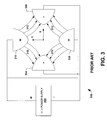
- FIG. 3 is a diagram illustrating an exemplary, conventional positive and negative bipolar electrostatic quadrupole lens 300 .
- the lens 300 includes a power supply 302 that provides a positive voltage and a negative voltage, substantially equal in magnitude. Additionally, the lens 300 includes a pair of negative electrodes 304 , 306 , located opposite each other, and a pair of positive electrodes 308 , 310 , located opposite each other, wherein the electrodes 304 , 306 , 308 , 310 are equally spaced about a center point.
- the negative electrode pair 304 , 306 is connected to the power supply 302 and receives the negative voltage. As a result, the negative electrode pair 304 , 306 is biased to a negative value. Additionally, the positive electrode pair 308 , 310 is connected to the power supply 302 and receives the positive voltage, and thus is biased to a positive voltage.
- the electrodes ( 304 , 306 , 308 , and 310 ) generate quadrupole electrostatic fields that selectively focus and defocus an ion beam that passes through the center point. As an example, positively charged ions in an ion beam are accelerated by the fields in the directions illustrated by the arrows 312 , resulting in ion beam focusing in the Y direction and defocusing in the X direction. The amount of focusing/defocusing obtained is a function of the magnitude of the positive and negative voltages that bias the electrodes ( 304 , 306 , 308 , and 310 ).
- FIG. 4 a diagram illustrating a negative unipolar electrostatic quadrupole lens 400 in accordance with an aspect of the present invention is depicted.
- the lens 400 includes a negative electrode pair 404 , 406 and a ground electrode pair 408 , 410 .
- a power supply 402 delivers a negative voltage to the negative electrode pair 408 , 410 .
- the ground electrode pair 408 , 410 are connected to ground, typically through a low resistance path. Accordingly, the negative electrode pair is biased to a negative voltage value and the ground electrode pair 408 , 410 is biased to ground.
- the electrodes generate electrostatic quadrupole fields in a manner similar to that illustrated in FIG. 3 , wherein the beam is focused in one plane and concurrently defocused in a second, perpendicular plane.
- the unipolar electrostatic quadrupole lens 400 mitigates loss of beam current due as compared to the bipolar positive and negative electrostatic quadrupole lens 300 of FIG. 3 . It is believed that the positive potential electrodes reduce the beam current loss by exacerbating space charge effects on the positively charge ions present in the ion beam. In any event, with use of the unipolar electrostatic lens of FIG. 3 , a two fold increase in resultant beam current has been observed in some instances at low energies.
- FIG. 5 a diagram illustrating a positive unipolar electrostatic quadrupole lens 500 in accordance with an aspect of the present invention is depicted.
- the lens 500 includes a first positive electrode 504 , a second positive electrode 506 , a first ground electrode 508 , and a second ground electrode 510 .
- a power supply 502 delivers a positive voltage to the first positive electrode 504 and the second positive electrode 506 .
- the first ground electrode 508 and the second ground electrode 510 are connected to ground. Accordingly, the first positive electrode 504 and the second positive electrode 506 are biased to a positive voltage value and the first ground electrode 508 and the second ground electrode 510 are biased to a ground voltage value.
- the electrodes generate quadrupole fields from the electrodes, two positive and two neutral. As an example, the two neutral (ground) fields tend to defocus positively charged ions of an ion beam whereas the two positive fields tend to focus the positively charged ions.
- the unipolar electrostatic quadrupole lens 500 mitigates loss of beam current due as compared to the bipolar positive and negative electrostatic quadrupole lens 300 of FIG. 3 .
- the negative unipolar electrostatic quadrupole lens 400 of FIG. 4 tends to mitigate current loss better than the positive unipolar electrostatic quadrupole lens 500 of FIG. 5 .
- FIG. 6 is a diagram illustrating a switching circuit of an electrostatic quadrupole lens 600 from unipolar to bipolar operation in accordance with an aspect of the present invention.
- a negative power supply 601 produces a negative voltage and a positive power supply 602 produces a positive voltage.
- the lens 600 comprises a first negative electrode 604 , a second negative electrode 606 , a first variable potential electrode 608 and a second variable potential electrode 610 .
- the first negative electrode 604 and the second negative electrode 606 receive the negative voltage from the negative power supply 601 and are thus, biased negative.
- the first variable potential electrode 608 and the second variable potential electrode 610 are either biased positive by the positive power supply 602 or biased to ground.
- a switch 612 is employed to control the biasing of the first variable potential electrode 608 and the second variable potential electrode 610 , respectively.
- the switch 612 is a single pole double throw switch between the positive power supply 602 and ground.
- the switch 612 can be operated manually or automatically via a control system (not shown).
- FIG. 7 is a diagram illustrating another switching circuit of an electrostatic quadrupole lens 700 from unipolar to bipolar operation in accordance with an aspect of the present invention.
- a negative power supply 701 produces a negative voltage and a positive power supply 702 produces a positive voltage.
- the lens 700 comprises a negative electrode pair 704 , 706 and a variable potential electrode pair 708 , 710 .
- the negative electrode pair 704 , 706 receives the negative voltage from the negative power supply 701 and is thus, biased negative.
- the variable potential electrode pair 708 , 710 is either biased positive by the positive power supply 702 or biased to ground.
- Switching circuitry 712 is included as part of the positive power supply 702 .
- the switching circuitry 712 is operable to controllably provide a power supply output that is either a positive voltage value or is a low resistance path to ground.
- the switching circuitry 712 is employed to control the biasing of the variable potential electrode pair 708 , 710 .
- FIGS. 6-7 depict two exemplary aspects of configuring an electrostatic quadrupole lens for dual and/or unipolar operation in accordance with the present invention.
- the present invention is not limited to these particular aspects and can be extended to include variations thereof, so long as the quadrupole lens can be selected to operate in dual or unipolar operation.
- FIGS. 6-7 are described with respect to a single negative unipolar electrostatic quadrupole lens, but can be extended to a single positive unipolar electrostatic quadrupole lens and be in accordance with the present invention.
- the unipolar electrostatic quadrupole lens can yield substantially more beam current that the conventional bipolar electrostatic quadrupole lens.
- the conventional bipolar electrostatic quadrupole lens yields only about 30 uA, whereas the positive unipolar electrostatic quadrupole lens yields about ⁇ 100 uA and the negative unipolar electrostatic quadrupole lens yields about 150 uA.
- the positive unipolar electrostatic quadrupole lens provides about three times or more beam current than the conventional bipolar electrostatic quadrupole lens and the negative unipolar electrostatic quadrupole lens provides about five times the beam current than the conventional bipolar electrostatic quadrupole lens.
- FIGS. 1-7 methodologies in accordance with various aspects of the present invention will be better appreciated with reference to FIGS. 1-7 . While, for purposes of simplicity of explanation, the methodologies of FIGS. 8-9 are depicted and described as executing serially, it is to be understood and appreciated that the present invention is not limited by the illustrated order, as some aspects could, in accordance with the present invention, occur in different orders and/or concurrently with other aspects from that depicted and described herein. Moreover, not all illustrated features may be required to implement a methodology in accordance with an aspect the present invention.
- FIG. 8 a flow diagram of a method 800 of generating a desired ion beam in accordance with an aspect of the present invention is depicted.
- the method 800 is able to generate a desired ion beam with reduced beam current loss through a linear accelerator as compared with conventional ion beam generation methods (e.g., conventional ion implantation devices).
- the method 800 is particularly suited for relatively low energy ion beams (e.g., less than 80 KeV).
- the method 800 begins at 802 wherein an ion beam comprised of positive or negative ions is generated by an ion source powered by a high voltage power supply.
- the ion beam is generated with an initial energy level and beam current, referred to as the injection current based, for example, on the biasing and configuration of the extraction beam associated with the ion source.
- the ion beam is then processed by a mass analyzer at block 804 , wherein a magnetic field permits substantially only ions that have a desired charge-to-mass ratio to pass.
- a magnetic field permits substantially only ions that have a desired charge-to-mass ratio to pass.
- One criteria for biasing the quadrupoles in the above condition is simply to maintain the bias arrangement within which the quadrupoles are currently configured. If, however, the desired energy of the beam is not greater than the second threshold (NO at 812 ), then a unipolar bias configuration of the quadrupoles is employed at 816 . As discussed above, use of a unipolar configuration at low energies advantageously facilitates improved beam current in the ion implantation system.
- Ions of the ion beam are selectively focused at block 808 by one or more unipolar electrostatic quadrupole lenses to yield an ion beam having a desired shape (e.g., symmetrical, oblong, and the like).
- the lenses are each comprised of two pairs of electrodes, all generally equally spaced about a center point through which the ion beam travels. A first opposing pair is biased to ground and a second opposing pair is biased to a positive or negative voltage.
- the electrodes generate quadrupole electric fields transverse to the path of the ion beam, thereby causing focusing and defocusing of the ion beam as previously discussed.
- the pair of lenses serve to maintain beam focus and mitigate space charge effects.
- the voltage value employed for biasing the second pair of electrodes is a function of desired focusing and defocusing.
- the ion beam is then directed at the wafer at 818 , wherein such action may further include beam deceleration, deflection, etc., as may be desired.
- the first threshold is about 80 keV and the second threshold is about 50 keV, however, other threshold values may be employed and are contemplated as falling within the scope of the present invention.
Abstract
Description
| 5 KeV energy, 420 uA injection current |
| Resulting current | |||
| Unipolar | negative | 150 | uA | ||
| Unipolar | positive | ˜100 | uA | ||
| Conventional | positive and | ˜30 | uA | ||
| bipolar | negative | ||||
Claims (16)
Priority Applications (7)
| Application Number | Priority Date | Filing Date | Title |
|---|---|---|---|
| US10/654,168 US6949895B2 (en) | 2003-09-03 | 2003-09-03 | Unipolar electrostatic quadrupole lens and switching methods for charged beam transport |
| KR1020067004443A KR101099943B1 (en) | 2003-09-03 | 2004-09-02 | Unipolar electrostatic quadrupole lens and switching methods for charged beam transport |
| JP2006525451A JP5013247B2 (en) | 2003-09-03 | 2004-09-02 | Electrostatic quadrupole lens system and linear acceleration system using the same |
| PCT/US2004/028656 WO2005024911A2 (en) | 2003-09-03 | 2004-09-02 | Unipolar electrostatic quadrupole lens and switching methods for charged beam transport |
| TW093126517A TWI358741B (en) | 2003-09-03 | 2004-09-02 | Unipolar electrostatic quadrupole lens and switchi |
| EP04783034A EP1661155A2 (en) | 2003-09-03 | 2004-09-02 | Unipolar electrostatic quadrupole lens and switching methods for charged beam transport |
| CN200480025420XA CN1846292B (en) | 2003-09-03 | 2004-09-02 | Unipolar electrostatic quadrupole lens and switching methods for charged beam transport |
Applications Claiming Priority (1)
| Application Number | Priority Date | Filing Date | Title |
|---|---|---|---|
| US10/654,168 US6949895B2 (en) | 2003-09-03 | 2003-09-03 | Unipolar electrostatic quadrupole lens and switching methods for charged beam transport |
Publications (2)
| Publication Number | Publication Date |
|---|---|
| US20050045835A1 US20050045835A1 (en) | 2005-03-03 |
| US6949895B2 true US6949895B2 (en) | 2005-09-27 |
Family
ID=34218029
Family Applications (1)
| Application Number | Title | Priority Date | Filing Date |
|---|---|---|---|
| US10/654,168 Expired - Lifetime US6949895B2 (en) | 2003-09-03 | 2003-09-03 | Unipolar electrostatic quadrupole lens and switching methods for charged beam transport |
Country Status (7)
| Country | Link |
|---|---|
| US (1) | US6949895B2 (en) |
| EP (1) | EP1661155A2 (en) |
| JP (1) | JP5013247B2 (en) |
| KR (1) | KR101099943B1 (en) |
| CN (1) | CN1846292B (en) |
| TW (1) | TWI358741B (en) |
| WO (1) | WO2005024911A2 (en) |
Cited By (9)
| Publication number | Priority date | Publication date | Assignee | Title |
|---|---|---|---|---|
| US20060113493A1 (en) * | 2004-11-30 | 2006-06-01 | Sumitomo Eaton Nova Corporation | Irradiation system ion beam and method to enhance accuracy of irradiation |
| US20090309039A1 (en) * | 2008-06-11 | 2009-12-17 | Solar Implant Technologies Inc. | Application specific implant system and method for use in solar cell fabrications |
| US8697552B2 (en) | 2009-06-23 | 2014-04-15 | Intevac, Inc. | Method for ion implant using grid assembly |
| US9318332B2 (en) | 2012-12-19 | 2016-04-19 | Intevac, Inc. | Grid for plasma ion implant |
| US9324598B2 (en) | 2011-11-08 | 2016-04-26 | Intevac, Inc. | Substrate processing system and method |
| US20220087004A1 (en) * | 2020-09-17 | 2022-03-17 | Applied Materials, Inc. | System, apparatus and method for multi-frequency resonator operation in linear accelerator |
| US20220174810A1 (en) * | 2020-12-01 | 2022-06-02 | Applied Materials, Inc. | Resonator, linear accelerator configuration and ion implantation system having toroidal resonator |
| US11476087B2 (en) * | 2020-08-03 | 2022-10-18 | Applied Materials, Inc. | Ion implantation system and linear accelerator having novel accelerator stage configuration |
| US20230083050A1 (en) * | 2021-09-13 | 2023-03-16 | Applied Materials, Inc. | Drift tube, apparatus and ion implanter having variable focus electrode in linear accelerator |
Families Citing this family (10)
| Publication number | Priority date | Publication date | Assignee | Title |
|---|---|---|---|---|
| US7402821B2 (en) * | 2006-01-18 | 2008-07-22 | Axcelis Technologies, Inc. | Application of digital frequency and phase synthesis for control of electrode voltage phase in a high-energy ion implantation machine, and a means for accurate calibration of electrode voltage phase |
| WO2009039884A1 (en) * | 2007-09-26 | 2009-04-02 | Ion Beam Applications S.A. | Particle beam transport apparatus and method of transporting a particle beam with small beam spot size |
| JP5331342B2 (en) * | 2008-01-11 | 2013-10-30 | 株式会社日立ハイテクノロジーズ | Ion milling equipment |
| US20110162703A1 (en) * | 2009-03-20 | 2011-07-07 | Solar Implant Technologies, Inc. | Advanced high efficientcy crystalline solar cell fabrication method |
| EP2534674B1 (en) * | 2010-02-09 | 2016-04-06 | Intevac, Inc. | An adjustable shadow mask assembly for use in solar cell fabrications |
| WO2012008255A1 (en) * | 2010-07-12 | 2012-01-19 | 三菱電機株式会社 | Drift tube linear accelerator |
| CN102800549B (en) * | 2011-05-26 | 2015-06-10 | 和舰科技(苏州)有限公司 | Ion implantation machine and ion implantation method |
| JP5142173B1 (en) * | 2011-06-30 | 2013-02-13 | 株式会社Quan Japan | Charged particle accelerator and charged particle acceleration method |
| WO2019099648A1 (en) | 2017-11-15 | 2019-05-23 | Corning Incorporated | Liquid lens systems |
| US10943767B1 (en) * | 2020-01-09 | 2021-03-09 | Applied Materials, Inc. | Digital sampling to control resonator frequency and phase in a LINAC |
Citations (10)
| Publication number | Priority date | Publication date | Assignee | Title |
|---|---|---|---|---|
| US2919381A (en) * | 1956-07-25 | 1959-12-29 | Farrand Optical Co Inc | Electron lens |
| US3147445A (en) * | 1959-11-05 | 1964-09-01 | Thompson Ramo Wooldridge Inc | Quadrupole focusing means for charged particle containment |
| US4560905A (en) * | 1984-04-16 | 1985-12-24 | The United States Of America As Represented By The United States Department Of Energy | Electrostatic quadrupole focused particle accelerating assembly with laminar flow beam |
| US4667111A (en) * | 1985-05-17 | 1987-05-19 | Eaton Corporation | Accelerator for ion implantation |
| US4736107A (en) | 1986-09-24 | 1988-04-05 | Eaton Corporation | Ion beam implanter scan control system |
| US4761559A (en) | 1986-09-24 | 1988-08-02 | Eaton Corporation | Ion beam implantation display method and apparatus |
| US4912421A (en) * | 1988-07-13 | 1990-03-27 | The United States Of America As Represented By The United States Department Of Energy | Variable energy constant current accelerator structure |
| US4914305A (en) | 1989-01-04 | 1990-04-03 | Eaton Corporation | Uniform cross section ion beam system |
| US5430359A (en) * | 1992-11-02 | 1995-07-04 | Science Applications International Corporation | Segmented vane radio-frequency quadrupole linear accelerator |
| US5554854A (en) | 1995-07-17 | 1996-09-10 | Eaton Corporation | In situ removal of contaminants from the interior surfaces of an ion beam implanter |
Family Cites Families (14)
| Publication number | Priority date | Publication date | Assignee | Title |
|---|---|---|---|---|
| ES2126573T3 (en) * | 1991-04-22 | 1999-04-01 | Otsuka Pharma Co Ltd | DERIVATIVE OF PYRAZOLE (1,5-A) PIRIMIDINE AND ANTI-INFLAMMATORY AGENT CONTAINING THIS DERIVATIVE. |
| JPH07118287B2 (en) * | 1992-08-10 | 1995-12-18 | 株式会社日立製作所 | Magnetic quadrupole lens, ion beam accelerator and ion beam decelerator using the same |
| JPH0828279B2 (en) * | 1993-05-10 | 1996-03-21 | 株式会社日立製作所 | External resonance type high frequency quadrupole accelerator |
| US5571813A (en) * | 1993-06-10 | 1996-11-05 | Beiersdorf-Lilly Gmbh | Fused pyrimidine compounds and their use as pharmaceuticals |
| CA2169719C (en) * | 1994-06-21 | 2002-04-16 | Yasuo Shoji | Pyrazolo[1,5-a]pyrimidine derivative |
| JPH08148095A (en) * | 1994-11-25 | 1996-06-07 | Hitachi Ltd | Electron gun and color cathode-ray tube provided with this electron gun |
| US5919815A (en) * | 1996-05-22 | 1999-07-06 | Neuromedica, Inc. | Taxane compounds and compositions |
| US6191131B1 (en) * | 1997-07-23 | 2001-02-20 | Dupont Pharmaceuticals Company | Azolo triazines and pyrimidines |
| US6262096B1 (en) * | 1997-11-12 | 2001-07-17 | Bristol-Myers Squibb Company | Aminothiazole inhibitors of cyclin dependent kinases |
| US6040321A (en) * | 1997-11-12 | 2000-03-21 | Bristol-Myers Squibb Company | Aminothiazole inhibitors of cyclin dependent kinases |
| US6413974B1 (en) * | 1998-02-26 | 2002-07-02 | Aventis Pharmaceuticals Inc. | 6,9,-disubstituted 2-[trans-(4-aminocyclohexyl) amino] purines |
| US6291828B1 (en) * | 1999-12-21 | 2001-09-18 | Axchlisrtechnologies, Inc. | Glass-like insulator for electrically isolating electrodes from ion implanter housing |
| DE60045439D1 (en) * | 2000-01-24 | 2011-02-10 | Integrated Circuit Testing | Bowl for a charged particle beam device |
| US6635890B2 (en) * | 2001-08-23 | 2003-10-21 | Axcelis Technologies, Inc. | Slit double gap buncher and method for improved ion bunching in an ion implantation system |
-
2003
- 2003-09-03 US US10/654,168 patent/US6949895B2/en not_active Expired - Lifetime
-
2004
- 2004-09-02 KR KR1020067004443A patent/KR101099943B1/en active IP Right Grant
- 2004-09-02 CN CN200480025420XA patent/CN1846292B/en not_active Expired - Fee Related
- 2004-09-02 JP JP2006525451A patent/JP5013247B2/en not_active Expired - Fee Related
- 2004-09-02 WO PCT/US2004/028656 patent/WO2005024911A2/en active Application Filing
- 2004-09-02 TW TW093126517A patent/TWI358741B/en not_active IP Right Cessation
- 2004-09-02 EP EP04783034A patent/EP1661155A2/en not_active Withdrawn
Patent Citations (11)
| Publication number | Priority date | Publication date | Assignee | Title |
|---|---|---|---|---|
| US2919381A (en) * | 1956-07-25 | 1959-12-29 | Farrand Optical Co Inc | Electron lens |
| US3147445A (en) * | 1959-11-05 | 1964-09-01 | Thompson Ramo Wooldridge Inc | Quadrupole focusing means for charged particle containment |
| US4560905A (en) * | 1984-04-16 | 1985-12-24 | The United States Of America As Represented By The United States Department Of Energy | Electrostatic quadrupole focused particle accelerating assembly with laminar flow beam |
| US4667111A (en) * | 1985-05-17 | 1987-05-19 | Eaton Corporation | Accelerator for ion implantation |
| US4667111C1 (en) * | 1985-05-17 | 2001-04-10 | Eaton Corp Cleveland | Accelerator for ion implantation |
| US4736107A (en) | 1986-09-24 | 1988-04-05 | Eaton Corporation | Ion beam implanter scan control system |
| US4761559A (en) | 1986-09-24 | 1988-08-02 | Eaton Corporation | Ion beam implantation display method and apparatus |
| US4912421A (en) * | 1988-07-13 | 1990-03-27 | The United States Of America As Represented By The United States Department Of Energy | Variable energy constant current accelerator structure |
| US4914305A (en) | 1989-01-04 | 1990-04-03 | Eaton Corporation | Uniform cross section ion beam system |
| US5430359A (en) * | 1992-11-02 | 1995-07-04 | Science Applications International Corporation | Segmented vane radio-frequency quadrupole linear accelerator |
| US5554854A (en) | 1995-07-17 | 1996-09-10 | Eaton Corporation | In situ removal of contaminants from the interior surfaces of an ion beam implanter |
Cited By (24)
| Publication number | Priority date | Publication date | Assignee | Title |
|---|---|---|---|---|
| US20060113493A1 (en) * | 2004-11-30 | 2006-06-01 | Sumitomo Eaton Nova Corporation | Irradiation system ion beam and method to enhance accuracy of irradiation |
| US7429743B2 (en) * | 2004-11-30 | 2008-09-30 | Sen Corporation | Irradiation system ion beam and method to enhance accuracy of irradiation |
| US8697553B2 (en) | 2008-06-11 | 2014-04-15 | Intevac, Inc | Solar cell fabrication with faceting and ion implantation |
| US20090308450A1 (en) * | 2008-06-11 | 2009-12-17 | Solar Implant Technologies Inc. | Solar cell fabrication with faceting and ion implantation |
| US20090308440A1 (en) * | 2008-06-11 | 2009-12-17 | Solar Implant Technologies Inc. | Formation of solar cell-selective emitter using implant and anneal method |
| CN102099870A (en) * | 2008-06-11 | 2011-06-15 | 因特瓦克公司 | Application specific implant system and method for use in solar cell fabrications |
| US8871619B2 (en) * | 2008-06-11 | 2014-10-28 | Intevac, Inc. | Application specific implant system and method for use in solar cell fabrications |
| US20090309039A1 (en) * | 2008-06-11 | 2009-12-17 | Solar Implant Technologies Inc. | Application specific implant system and method for use in solar cell fabrications |
| US9741894B2 (en) | 2009-06-23 | 2017-08-22 | Intevac, Inc. | Ion implant system having grid assembly |
| US8697552B2 (en) | 2009-06-23 | 2014-04-15 | Intevac, Inc. | Method for ion implant using grid assembly |
| US8749053B2 (en) | 2009-06-23 | 2014-06-10 | Intevac, Inc. | Plasma grid implant system for use in solar cell fabrications |
| US8997688B2 (en) | 2009-06-23 | 2015-04-07 | Intevac, Inc. | Ion implant system having grid assembly |
| US9303314B2 (en) | 2009-06-23 | 2016-04-05 | Intevac, Inc. | Ion implant system having grid assembly |
| US9324598B2 (en) | 2011-11-08 | 2016-04-26 | Intevac, Inc. | Substrate processing system and method |
| US9875922B2 (en) | 2011-11-08 | 2018-01-23 | Intevac, Inc. | Substrate processing system and method |
| US9318332B2 (en) | 2012-12-19 | 2016-04-19 | Intevac, Inc. | Grid for plasma ion implant |
| US9583661B2 (en) | 2012-12-19 | 2017-02-28 | Intevac, Inc. | Grid for plasma ion implant |
| US11476087B2 (en) * | 2020-08-03 | 2022-10-18 | Applied Materials, Inc. | Ion implantation system and linear accelerator having novel accelerator stage configuration |
| US20220087004A1 (en) * | 2020-09-17 | 2022-03-17 | Applied Materials, Inc. | System, apparatus and method for multi-frequency resonator operation in linear accelerator |
| US11388810B2 (en) * | 2020-09-17 | 2022-07-12 | Applied Materials, Inc. | System, apparatus and method for multi-frequency resonator operation in linear accelerator |
| US20220174810A1 (en) * | 2020-12-01 | 2022-06-02 | Applied Materials, Inc. | Resonator, linear accelerator configuration and ion implantation system having toroidal resonator |
| US11596051B2 (en) * | 2020-12-01 | 2023-02-28 | Applied Materials, Inc. | Resonator, linear accelerator configuration and ion implantation system having toroidal resonator |
| US20230083050A1 (en) * | 2021-09-13 | 2023-03-16 | Applied Materials, Inc. | Drift tube, apparatus and ion implanter having variable focus electrode in linear accelerator |
| US11825590B2 (en) * | 2021-09-13 | 2023-11-21 | Applied Materials, Inc. | Drift tube, apparatus and ion implanter having variable focus electrode in linear accelerator |
Also Published As
| Publication number | Publication date |
|---|---|
| TWI358741B (en) | 2012-02-21 |
| KR20060123082A (en) | 2006-12-01 |
| JP5013247B2 (en) | 2012-08-29 |
| US20050045835A1 (en) | 2005-03-03 |
| WO2005024911A3 (en) | 2005-07-21 |
| CN1846292B (en) | 2010-11-24 |
| KR101099943B1 (en) | 2011-12-28 |
| EP1661155A2 (en) | 2006-05-31 |
| WO2005024911A2 (en) | 2005-03-17 |
| JP2007504622A (en) | 2007-03-01 |
| TW200531133A (en) | 2005-09-16 |
| CN1846292A (en) | 2006-10-11 |
Similar Documents
| Publication | Publication Date | Title |
|---|---|---|
| US6949895B2 (en) | Unipolar electrostatic quadrupole lens and switching methods for charged beam transport | |
| JP4521850B2 (en) | Acceleration and analysis architecture for ion implanters | |
| JP5689415B2 (en) | Magnetic energy filter after decel in ion implantation system | |
| US7579605B2 (en) | Multi-purpose electrostatic lens for an ion implanter system | |
| US6534775B1 (en) | Electrostatic trap for particles entrained in an ion beam | |
| US5300891A (en) | Ion accelerator | |
| US20180218894A1 (en) | Ion Mass Separation Using RF Extraction | |
| KR101242463B1 (en) | Weakening focusing effect of acceleration-deceleration column of ion implanter | |
| US6525326B1 (en) | System and method for removing particles entrained in an ion beam | |
| WO2007059227A2 (en) | Technique for providing a segmented electrostatic lens in an ion implanter | |
| US6476399B1 (en) | System and method for removing contaminant particles relative to an ion beam | |
| JP2023537472A (en) | Linear accelerator with ion implantation system and novel accelerator stage configuration | |
| US6897457B1 (en) | Apparatus and method for monitoring and tuning an ion beam in ion implantation apparatus | |
| WO2003019613A1 (en) | Method and apparatus for improved ion bunching in an ion implantation system | |
| JP2012523092A (en) | Termination for electrodes used in ion implantation systems | |
| JP2713692B2 (en) | Ion implantation equipment | |
| Satoh | Acceleration of 4+ ions in an RF Linac Accelerator | |
| KR20210105374A (en) | Quadrapole extraction device for ion source |
Legal Events
| Date | Code | Title | Description |
|---|---|---|---|
| AS | Assignment |
Owner name: AXCELIS TECHNOLOGIES, INC., MASSACHUSETTS Free format text: ASSIGNMENT OF ASSIGNORS INTEREST;ASSIGNORS:DIVERGILIO, WILLIAM F.;HUANG, YOUNGZHANG;REEL/FRAME:014477/0466 Effective date: 20030903 |
|
| AS | Assignment |
Owner name: PHARMACOPEIA DRUG DISCOVERY, NEW JERSEY Free format text: ASSIGNMENT OF ASSIGNORS INTEREST;ASSIGNOR:PHARMACOPEIA INC.;REEL/FRAME:015144/0732 Effective date: 20040330 |
|
| STCF | Information on status: patent grant |
Free format text: PATENTED CASE |
|
| AS | Assignment |
Owner name: SILICON VALLEY BANK, CALIFORNIA Free format text: SECURITY AGREEMENT;ASSIGNOR:AXCELIS TECHNOLOGIES, INC.;REEL/FRAME:020986/0143 Effective date: 20080423 Owner name: SILICON VALLEY BANK,CALIFORNIA Free format text: SECURITY AGREEMENT;ASSIGNOR:AXCELIS TECHNOLOGIES, INC.;REEL/FRAME:020986/0143 Effective date: 20080423 |
|
| FPAY | Fee payment |
Year of fee payment: 4 |
|
| AS | Assignment |
Owner name: SEN CORPORATION, JAPAN Free format text: CONSENT AND LICENSE AGREEMENT;ASSIGNOR:AXCELIS TECHNOLOGIES, INC.;REEL/FRAME:022562/0758 Effective date: 20090330 Owner name: SEN CORPORATION,JAPAN Free format text: CONSENT AND LICENSE AGREEMENT;ASSIGNOR:AXCELIS TECHNOLOGIES, INC.;REEL/FRAME:022562/0758 Effective date: 20090330 |
|
| FPAY | Fee payment |
Year of fee payment: 8 |
|
| FPAY | Fee payment |
Year of fee payment: 12 |
|
| AS | Assignment |
Owner name: SILICON VALLEY BANK, AS ADMINISTRATIVE AGENT, CALIFORNIA Free format text: SECURITY INTEREST;ASSIGNOR:AXCELIS TECHNOLOGIES, INC.;REEL/FRAME:053375/0055 Effective date: 20200731 |
|
| AS | Assignment |
Owner name: AXCELIS TECHNOLOGIES, INC., MASSACHUSETTS Free format text: RELEASE BY SECURED PARTY;ASSIGNOR:SILICON VALLEY BANK A DIVISION OF FIRST-CITIZENS BANK & TRUST COMPANY;REEL/FRAME:063270/0277 Effective date: 20230405 |