US6956256B2 - Vertical gain cell - Google Patents
Vertical gain cell Download PDFInfo
- Publication number
- US6956256B2 US6956256B2 US10/379,478 US37947803A US6956256B2 US 6956256 B2 US6956256 B2 US 6956256B2 US 37947803 A US37947803 A US 37947803A US 6956256 B2 US6956256 B2 US 6956256B2
- Authority
- US
- United States
- Prior art keywords
- vertical
- mos transistor
- transistor
- vertical mos
- cell
- Prior art date
- Legal status (The legal status is an assumption and is not a legal conclusion. Google has not performed a legal analysis and makes no representation as to the accuracy of the status listed.)
- Expired - Lifetime
Links
- 230000015654 memory Effects 0.000 claims abstract description 91
- 238000007667 floating Methods 0.000 claims abstract description 68
- 239000000758 substrate Substances 0.000 claims description 31
- 210000000746 body region Anatomy 0.000 claims description 6
- 230000008859 change Effects 0.000 claims description 5
- 239000003990 capacitor Substances 0.000 description 25
- 238000003860 storage Methods 0.000 description 20
- 239000004065 semiconductor Substances 0.000 description 15
- 229910021420 polycrystalline silicon Inorganic materials 0.000 description 12
- 229920005591 polysilicon Polymers 0.000 description 12
- 235000012431 wafers Nutrition 0.000 description 12
- XUIMIQQOPSSXEZ-UHFFFAOYSA-N Silicon Chemical compound [Si] XUIMIQQOPSSXEZ-UHFFFAOYSA-N 0.000 description 11
- 229910052710 silicon Inorganic materials 0.000 description 11
- 239000010703 silicon Substances 0.000 description 11
- 239000004020 conductor Substances 0.000 description 9
- 230000003321 amplification Effects 0.000 description 8
- 238000003199 nucleic acid amplification method Methods 0.000 description 8
- 230000015556 catabolic process Effects 0.000 description 7
- 239000012212 insulator Substances 0.000 description 7
- 239000000463 material Substances 0.000 description 6
- 238000010586 diagram Methods 0.000 description 5
- 238000012546 transfer Methods 0.000 description 5
- VYPSYNLAJGMNEJ-UHFFFAOYSA-N Silicium dioxide Chemical compound O=[Si]=O VYPSYNLAJGMNEJ-UHFFFAOYSA-N 0.000 description 4
- 239000003989 dielectric material Substances 0.000 description 4
- 238000013461 design Methods 0.000 description 3
- 238000000034 method Methods 0.000 description 3
- 238000012545 processing Methods 0.000 description 3
- 230000009467 reduction Effects 0.000 description 3
- 238000004891 communication Methods 0.000 description 2
- 238000006731 degradation reaction Methods 0.000 description 2
- 238000000151 deposition Methods 0.000 description 2
- 230000008021 deposition Effects 0.000 description 2
- 230000000694 effects Effects 0.000 description 2
- 230000005669 field effect Effects 0.000 description 2
- 230000006870 function Effects 0.000 description 2
- 238000002955 isolation Methods 0.000 description 2
- 238000005304 joining Methods 0.000 description 2
- 238000004519 manufacturing process Methods 0.000 description 2
- 239000007769 metal material Substances 0.000 description 2
- 150000004767 nitrides Chemical class 0.000 description 2
- 235000012239 silicon dioxide Nutrition 0.000 description 2
- 239000000377 silicon dioxide Substances 0.000 description 2
- -1 600-1 Chemical compound 0.000 description 1
- 229910052581 Si3N4 Inorganic materials 0.000 description 1
- 230000003213 activating effect Effects 0.000 description 1
- 230000006978 adaptation Effects 0.000 description 1
- LBDSXVIYZYSRII-IGMARMGPSA-N alpha-particle Chemical compound [4He+2] LBDSXVIYZYSRII-IGMARMGPSA-N 0.000 description 1
- 238000013459 approach Methods 0.000 description 1
- 239000000969 carrier Substances 0.000 description 1
- 238000007796 conventional method Methods 0.000 description 1
- 230000008878 coupling Effects 0.000 description 1
- 238000010168 coupling process Methods 0.000 description 1
- 238000005859 coupling reaction Methods 0.000 description 1
- 238000013500 data storage Methods 0.000 description 1
- 230000007423 decrease Effects 0.000 description 1
- 230000003247 decreasing effect Effects 0.000 description 1
- 238000001514 detection method Methods 0.000 description 1
- 238000011161 development Methods 0.000 description 1
- 238000009792 diffusion process Methods 0.000 description 1
- 239000002019 doping agent Substances 0.000 description 1
- 230000005684 electric field Effects 0.000 description 1
- 238000005516 engineering process Methods 0.000 description 1
- 230000036039 immunity Effects 0.000 description 1
- 238000002347 injection Methods 0.000 description 1
- 239000007924 injection Substances 0.000 description 1
- 230000000670 limiting effect Effects 0.000 description 1
- 230000000873 masking effect Effects 0.000 description 1
- 238000005272 metallurgy Methods 0.000 description 1
- 230000003647 oxidation Effects 0.000 description 1
- 238000007254 oxidation reaction Methods 0.000 description 1
- 230000003071 parasitic effect Effects 0.000 description 1
- 239000002245 particle Substances 0.000 description 1
- 230000002093 peripheral effect Effects 0.000 description 1
- 238000004886 process control Methods 0.000 description 1
- 230000005855 radiation Effects 0.000 description 1
- 230000002441 reversible effect Effects 0.000 description 1
- 238000000926 separation method Methods 0.000 description 1
- HQVNEWCFYHHQES-UHFFFAOYSA-N silicon nitride Chemical compound N12[Si]34N5[Si]62N3[Si]51N64 HQVNEWCFYHHQES-UHFFFAOYSA-N 0.000 description 1
- 239000007787 solid Substances 0.000 description 1
- 230000003068 static effect Effects 0.000 description 1
- 239000000126 substance Substances 0.000 description 1
Images


Classifications
-
- H—ELECTRICITY
- H10—SEMICONDUCTOR DEVICES; ELECTRIC SOLID-STATE DEVICES NOT OTHERWISE PROVIDED FOR
- H10B—ELECTRONIC MEMORY DEVICES
- H10B12/00—Dynamic random access memory [DRAM] devices
-
- H—ELECTRICITY
- H01—ELECTRIC ELEMENTS
- H01L—SEMICONDUCTOR DEVICES NOT COVERED BY CLASS H10
- H01L29/00—Semiconductor devices adapted for rectifying, amplifying, oscillating or switching, or capacitors or resistors with at least one potential-jump barrier or surface barrier, e.g. PN junction depletion layer or carrier concentration layer; Details of semiconductor bodies or of electrodes thereof ; Multistep manufacturing processes therefor
- H01L29/66—Types of semiconductor device ; Multistep manufacturing processes therefor
- H01L29/68—Types of semiconductor device ; Multistep manufacturing processes therefor controllable by only the electric current supplied, or only the electric potential applied, to an electrode which does not carry the current to be rectified, amplified or switched
- H01L29/76—Unipolar devices, e.g. field effect transistors
- H01L29/772—Field effect transistors
- H01L29/78—Field effect transistors with field effect produced by an insulated gate
- H01L29/7841—Field effect transistors with field effect produced by an insulated gate with floating body, e.g. programmable transistors
-
- H—ELECTRICITY
- H10—SEMICONDUCTOR DEVICES; ELECTRIC SOLID-STATE DEVICES NOT OTHERWISE PROVIDED FOR
- H10B—ELECTRONIC MEMORY DEVICES
- H10B12/00—Dynamic random access memory [DRAM] devices
- H10B12/20—DRAM devices comprising floating-body transistors, e.g. floating-body cells
-
- H—ELECTRICITY
- H01—ELECTRIC ELEMENTS
- H01L—SEMICONDUCTOR DEVICES NOT COVERED BY CLASS H10
- H01L27/00—Devices consisting of a plurality of semiconductor or other solid-state components formed in or on a common substrate
- H01L27/02—Devices consisting of a plurality of semiconductor or other solid-state components formed in or on a common substrate including semiconductor components specially adapted for rectifying, oscillating, amplifying or switching and having at least one potential-jump barrier or surface barrier; including integrated passive circuit elements with at least one potential-jump barrier or surface barrier
- H01L27/04—Devices consisting of a plurality of semiconductor or other solid-state components formed in or on a common substrate including semiconductor components specially adapted for rectifying, oscillating, amplifying or switching and having at least one potential-jump barrier or surface barrier; including integrated passive circuit elements with at least one potential-jump barrier or surface barrier the substrate being a semiconductor body
- H01L27/06—Devices consisting of a plurality of semiconductor or other solid-state components formed in or on a common substrate including semiconductor components specially adapted for rectifying, oscillating, amplifying or switching and having at least one potential-jump barrier or surface barrier; including integrated passive circuit elements with at least one potential-jump barrier or surface barrier the substrate being a semiconductor body including a plurality of individual components in a non-repetitive configuration
- H01L27/07—Devices consisting of a plurality of semiconductor or other solid-state components formed in or on a common substrate including semiconductor components specially adapted for rectifying, oscillating, amplifying or switching and having at least one potential-jump barrier or surface barrier; including integrated passive circuit elements with at least one potential-jump barrier or surface barrier the substrate being a semiconductor body including a plurality of individual components in a non-repetitive configuration the components having an active region in common
- H01L27/0705—Devices consisting of a plurality of semiconductor or other solid-state components formed in or on a common substrate including semiconductor components specially adapted for rectifying, oscillating, amplifying or switching and having at least one potential-jump barrier or surface barrier; including integrated passive circuit elements with at least one potential-jump barrier or surface barrier the substrate being a semiconductor body including a plurality of individual components in a non-repetitive configuration the components having an active region in common comprising components of the field effect type
-
- H—ELECTRICITY
- H10—SEMICONDUCTOR DEVICES; ELECTRIC SOLID-STATE DEVICES NOT OTHERWISE PROVIDED FOR
- H10B—ELECTRONIC MEMORY DEVICES
- H10B12/00—Dynamic random access memory [DRAM] devices
- H10B12/30—DRAM devices comprising one-transistor - one-capacitor [1T-1C] memory cells
- H10B12/39—DRAM devices comprising one-transistor - one-capacitor [1T-1C] memory cells the capacitor and the transistor being in a same trench
- H10B12/395—DRAM devices comprising one-transistor - one-capacitor [1T-1C] memory cells the capacitor and the transistor being in a same trench the transistor being vertical
Definitions
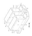
- each vertical gain cell 401 - 1 , 401 - 2 is configured on write data/bit line 423 . Further, each vertical gain cell 401 - 1 , 401 - 2 is coupled to read data/bit line 417 . However, each vertical gain cell 401 - 1 , 401 - 2 disposed on write data/bit line 423 is addressed with a separate write data word line and a separate read data word line, which correspond to different rows of the array.
- FIG. 4C illustrates a three dimensional view of an embodiment of DRAM cells 401 - 1 , 401 - 2 as shown in FIG. 4 A.
- FIG. 4C illustrates the use of these vertical gain cells in an array of memory cells.
- Vertical gain cells disposed on a common write data/bit line 423 with each of these vertical gain cells coupled to a common read data/bit line 417 , form a column in the memory array, where the number of columns correspond to the number of separate write data/bit lines.
Abstract
Description
Claims (41)
Priority Applications (4)
| Application Number | Priority Date | Filing Date | Title |
|---|---|---|---|
| US10/379,478 US6956256B2 (en) | 2003-03-04 | 2003-03-04 | Vertical gain cell |
| US10/931,545 US7241658B2 (en) | 2003-03-04 | 2004-08-31 | Vertical gain cell |
| US10/931,573 US7298638B2 (en) | 2003-03-04 | 2004-08-31 | Operating an electronic device having a vertical gain cell that includes vertical MOS transistors |
| US11/689,896 US7528440B2 (en) | 2003-03-04 | 2007-03-22 | Vertical gain cell |
Applications Claiming Priority (1)
| Application Number | Priority Date | Filing Date | Title |
|---|---|---|---|
| US10/379,478 US6956256B2 (en) | 2003-03-04 | 2003-03-04 | Vertical gain cell |
Related Child Applications (2)
| Application Number | Title | Priority Date | Filing Date |
|---|---|---|---|
| US10/931,545 Division US7241658B2 (en) | 2003-03-04 | 2004-08-31 | Vertical gain cell |
| US10/931,573 Division US7298638B2 (en) | 2003-03-04 | 2004-08-31 | Operating an electronic device having a vertical gain cell that includes vertical MOS transistors |
Publications (2)
| Publication Number | Publication Date |
|---|---|
| US20040174734A1 US20040174734A1 (en) | 2004-09-09 |
| US6956256B2 true US6956256B2 (en) | 2005-10-18 |
Family
ID=32926686
Family Applications (4)
| Application Number | Title | Priority Date | Filing Date |
|---|---|---|---|
| US10/379,478 Expired - Lifetime US6956256B2 (en) | 2003-03-04 | 2003-03-04 | Vertical gain cell |
| US10/931,573 Expired - Lifetime US7298638B2 (en) | 2003-03-04 | 2004-08-31 | Operating an electronic device having a vertical gain cell that includes vertical MOS transistors |
| US10/931,545 Expired - Lifetime US7241658B2 (en) | 2003-03-04 | 2004-08-31 | Vertical gain cell |
| US11/689,896 Expired - Lifetime US7528440B2 (en) | 2003-03-04 | 2007-03-22 | Vertical gain cell |
Family Applications After (3)
| Application Number | Title | Priority Date | Filing Date |
|---|---|---|---|
| US10/931,573 Expired - Lifetime US7298638B2 (en) | 2003-03-04 | 2004-08-31 | Operating an electronic device having a vertical gain cell that includes vertical MOS transistors |
| US10/931,545 Expired - Lifetime US7241658B2 (en) | 2003-03-04 | 2004-08-31 | Vertical gain cell |
| US11/689,896 Expired - Lifetime US7528440B2 (en) | 2003-03-04 | 2007-03-22 | Vertical gain cell |
Country Status (1)
| Country | Link |
|---|---|
| US (4) | US6956256B2 (en) |
Cited By (21)
| Publication number | Priority date | Publication date | Assignee | Title |
|---|---|---|---|---|
| US20040042256A1 (en) * | 2002-08-29 | 2004-03-04 | Micron Technology, Inc. | Single transistor vertical memory gain cell |
| US20050024936A1 (en) * | 2003-03-04 | 2005-02-03 | Micron Technology, Inc. | Vertical gain cell |
| US20060013042A1 (en) * | 2004-07-19 | 2006-01-19 | Micron Technology, Inc. | In-service reconfigurable dram and flash memory device |
| US20060134868A1 (en) * | 2003-09-16 | 2006-06-22 | Samsung Electronics Co., Ltd. | Double gate field effect transistor and method of manufacturing the same |
| US20060278926A1 (en) * | 2005-06-08 | 2006-12-14 | Suraj Mathew | Capacitorless DRAM on bulk silicon |
| KR100726150B1 (en) | 2005-12-29 | 2007-06-13 | 주식회사 하이닉스반도체 | Method for manufacturing saddle type fin transistor |
| US20070152255A1 (en) * | 2005-11-17 | 2007-07-05 | Hyeoung-Won Seo | Semiconductor memory device having vertical channel transistor and method for fabricating the same |
| US7452763B1 (en) * | 2003-03-04 | 2008-11-18 | Qspeed Semiconductor Inc. | Method for a junction field effect transistor with reduced gate capacitance |
| US7564087B2 (en) | 2002-08-29 | 2009-07-21 | Micron Technology, Inc. | Merged MOS-bipolar capacitor memory cell |
| US20100176451A1 (en) * | 2009-01-09 | 2010-07-15 | Hoon Jeong | Semiconductor |
| US20100276749A1 (en) * | 2004-09-01 | 2010-11-04 | Micron Technology, Inc. | Vertical transistors |
| US8441053B2 (en) | 2010-10-15 | 2013-05-14 | Powerchip Technology Corporation | Vertical capacitor-less DRAM cell, DRAM array and operation of the same |
| US20140138600A1 (en) * | 2011-11-21 | 2014-05-22 | Kimihiro Satoh | Memory device having stitched arrays of 4 f² memory cells |
| US8767458B2 (en) * | 2010-11-16 | 2014-07-01 | Zeno Semiconductor, Inc. | Dual-port semiconductor memory and first in first out (FIFO) memory having electrically floating body transistor |
| US20150155282A1 (en) * | 2011-02-17 | 2015-06-04 | Semiconductor Energy Laboratory Co., Ltd. | Semiconductor memory device and method of manufacturing semiconductor memory device |
| US9153333B2 (en) | 2007-10-24 | 2015-10-06 | Zeno Semiconductor, Inc. | Semiconductor memory having both volatile and non-volatile functionality and method of operating |
| US9281022B2 (en) | 2013-07-10 | 2016-03-08 | Zeno Semiconductor, Inc. | Systems and methods for reducing standby power in floating body memory devices |
| US9905564B2 (en) | 2012-02-16 | 2018-02-27 | Zeno Semiconductors, Inc. | Memory cell comprising first and second transistors and methods of operating |
| US10515801B2 (en) | 2007-06-04 | 2019-12-24 | Micron Technology, Inc. | Pitch multiplication using self-assembling materials |
| US10727253B1 (en) | 2019-02-04 | 2020-07-28 | Globalfoundries Inc. | Simplified memory cells based on fully-depleted silicon-on-insulator transistors |
| US20210327883A1 (en) * | 2019-03-06 | 2021-10-21 | Micron Technology, Inc. | Integrated Assemblies Having Shield Lines Between Digit Lines, and Methods of Forming Integrated Assemblies |
Families Citing this family (83)
| Publication number | Priority date | Publication date | Assignee | Title |
|---|---|---|---|---|
| US7030436B2 (en) * | 2002-12-04 | 2006-04-18 | Micron Technology, Inc. | Embedded DRAM gain memory cell having MOS transistor body provided with a bi-polar transistor charge injecting means |
| US7091566B2 (en) * | 2003-11-20 | 2006-08-15 | International Business Machines Corp. | Dual gate FinFet |
| US7148538B2 (en) * | 2003-12-17 | 2006-12-12 | Micron Technology, Inc. | Vertical NAND flash memory array |
| US7253650B2 (en) * | 2004-05-25 | 2007-08-07 | International Business Machines Corporation | Increase productivity at wafer test using probe retest data analysis |
| US7098105B2 (en) * | 2004-05-26 | 2006-08-29 | Micron Technology, Inc. | Methods for forming semiconductor structures |
| US7547945B2 (en) * | 2004-09-01 | 2009-06-16 | Micron Technology, Inc. | Transistor devices, transistor structures and semiconductor constructions |
| US7271433B1 (en) | 2004-09-02 | 2007-09-18 | Micron Technology, Inc. | High-density single transistor vertical memory gain cell |
| US7259415B1 (en) | 2004-09-02 | 2007-08-21 | Micron Technology, Inc. | Long retention time single transistor vertical memory gain cell |
| US7271052B1 (en) * | 2004-09-02 | 2007-09-18 | Micron Technology, Inc. | Long retention time single transistor vertical memory gain cell |
| US7199419B2 (en) * | 2004-12-13 | 2007-04-03 | Micron Technology, Inc. | Memory structure for reduced floating body effect |
| US7326611B2 (en) * | 2005-02-03 | 2008-02-05 | Micron Technology, Inc. | DRAM arrays, vertical transistor structures and methods of forming transistor structures and DRAM arrays |
| KR100702014B1 (en) * | 2005-05-03 | 2007-03-30 | 삼성전자주식회사 | One-transistor floating-body DRAM devices having vertical channel transistor structure and methods of fabricating the same |
| US7282401B2 (en) | 2005-07-08 | 2007-10-16 | Micron Technology, Inc. | Method and apparatus for a self-aligned recessed access device (RAD) transistor gate |
| US7867851B2 (en) | 2005-08-30 | 2011-01-11 | Micron Technology, Inc. | Methods of forming field effect transistors on substrates |
| US7301210B2 (en) * | 2006-01-12 | 2007-11-27 | International Business Machines Corporation | Method and structure to process thick and thin fins and variable fin to fin spacing |
| US7700441B2 (en) | 2006-02-02 | 2010-04-20 | Micron Technology, Inc. | Methods of forming field effect transistors, methods of forming field effect transistor gates, methods of forming integrated circuitry comprising a transistor gate array and circuitry peripheral to the gate array, and methods of forming integrated circuitry comprising a transistor gate array including first gates and second grounded isolation gates |
| US7542345B2 (en) * | 2006-02-16 | 2009-06-02 | Innovative Silicon Isi Sa | Multi-bit memory cell having electrically floating body transistor, and method of programming and reading same |
| US8501581B2 (en) * | 2006-03-29 | 2013-08-06 | Micron Technology, Inc. | Methods of forming semiconductor constructions |
| US7491995B2 (en) * | 2006-04-04 | 2009-02-17 | Micron Technology, Inc. | DRAM with nanofin transistors |
| US8354311B2 (en) | 2006-04-04 | 2013-01-15 | Micron Technology, Inc. | Method for forming nanofin transistors |
| US8734583B2 (en) * | 2006-04-04 | 2014-05-27 | Micron Technology, Inc. | Grown nanofin transistors |
| US7425491B2 (en) * | 2006-04-04 | 2008-09-16 | Micron Technology, Inc. | Nanowire transistor with surrounding gate |
| US20070228491A1 (en) * | 2006-04-04 | 2007-10-04 | Micron Technology, Inc. | Tunneling transistor with sublithographic channel |
| US7602001B2 (en) | 2006-07-17 | 2009-10-13 | Micron Technology, Inc. | Capacitorless one transistor DRAM cell, integrated circuitry comprising an array of capacitorless one transistor DRAM cells, and method of forming lines of capacitorless one transistor DRAM cells |
| US7772632B2 (en) | 2006-08-21 | 2010-08-10 | Micron Technology, Inc. | Memory arrays and methods of fabricating memory arrays |
| US7589995B2 (en) | 2006-09-07 | 2009-09-15 | Micron Technology, Inc. | One-transistor memory cell with bias gate |
| US9601493B2 (en) | 2006-11-29 | 2017-03-21 | Zeno Semiconductor, Inc | Compact semiconductor memory device having reduced number of contacts, methods of operating and methods of making |
| US8077536B2 (en) * | 2008-08-05 | 2011-12-13 | Zeno Semiconductor, Inc. | Method of operating semiconductor memory device with floating body transistor using silicon controlled rectifier principle |
| US9391079B2 (en) | 2007-11-29 | 2016-07-12 | Zeno Semiconductor, Inc. | Compact semiconductor memory device having reduced number of contacts, methods of operating and methods of making |
| US8547756B2 (en) | 2010-10-04 | 2013-10-01 | Zeno Semiconductor, Inc. | Semiconductor memory device having an electrically floating body transistor |
| US8159868B2 (en) | 2008-08-22 | 2012-04-17 | Zeno Semiconductor, Inc. | Semiconductor memory having both volatile and non-volatile functionality including resistance change material and method of operating |
| US7760548B2 (en) | 2006-11-29 | 2010-07-20 | Yuniarto Widjaja | Semiconductor memory having both volatile and non-volatile functionality and method of operating |
| US8514622B2 (en) | 2007-11-29 | 2013-08-20 | Zeno Semiconductor, Inc. | Compact semiconductor memory device having reduced number of contacts, methods of operating and methods of making |
| US8194451B2 (en) | 2007-11-29 | 2012-06-05 | Zeno Semiconductor, Inc. | Memory cells, memory cell arrays, methods of using and methods of making |
| US20080277738A1 (en) * | 2007-05-08 | 2008-11-13 | Venkat Ananthan | Memory cells, memory banks, memory arrays, and electronic systems |
| US20090128991A1 (en) * | 2007-11-21 | 2009-05-21 | Micron Technology, Inc. | Methods and apparatuses for stacked capacitors for image sensors |
| US10403361B2 (en) | 2007-11-29 | 2019-09-03 | Zeno Semiconductor, Inc. | Memory cells, memory cell arrays, methods of using and methods of making |
| US8130547B2 (en) | 2007-11-29 | 2012-03-06 | Zeno Semiconductor, Inc. | Method of maintaining the state of semiconductor memory having electrically floating body transistor |
| US8174886B2 (en) | 2007-11-29 | 2012-05-08 | Zeno Semiconductor, Inc. | Semiconductor memory having electrically floating body transistor |
| US8264875B2 (en) | 2010-10-04 | 2012-09-11 | Zeno Semiconducor, Inc. | Semiconductor memory device having an electrically floating body transistor |
| US8130548B2 (en) * | 2007-11-29 | 2012-03-06 | Zeno Semiconductor, Inc. | Semiconductor memory having electrically floating body transistor |
| US8546876B2 (en) | 2008-03-20 | 2013-10-01 | Micron Technology, Inc. | Systems and devices including multi-transistor cells and methods of using, making, and operating the same |
| US7969776B2 (en) | 2008-04-03 | 2011-06-28 | Micron Technology, Inc. | Data cells with drivers and methods of making and operating the same |
| US8014200B2 (en) | 2008-04-08 | 2011-09-06 | Zeno Semiconductor, Inc. | Semiconductor memory having volatile and multi-bit, non-volatile functionality and methods of operating |
| KR100945511B1 (en) | 2008-04-10 | 2010-03-09 | 주식회사 하이닉스반도체 | Semiconductor device and method for manufacturing the same |
| TWI368299B (en) * | 2008-08-15 | 2012-07-11 | Nanya Technology Corp | Vertical transistor and array of vertical transistor |
| USRE47381E1 (en) | 2008-09-03 | 2019-05-07 | Zeno Semiconductor, Inc. | Forming semiconductor cells with regions of varying conductivity |
| US11908899B2 (en) | 2009-02-20 | 2024-02-20 | Zeno Semiconductor, Inc. | MOSFET and memory cell having improved drain current through back bias application |
| JP4487221B1 (en) * | 2009-04-17 | 2010-06-23 | 日本ユニサンティスエレクトロニクス株式会社 | Semiconductor device |
| US8139418B2 (en) * | 2009-04-27 | 2012-03-20 | Micron Technology, Inc. | Techniques for controlling a direct injection semiconductor memory device |
| US8537610B2 (en) * | 2009-07-10 | 2013-09-17 | Micron Technology, Inc. | Techniques for providing a semiconductor memory device |
| EP2532005A4 (en) | 2010-02-07 | 2016-06-22 | Zeno Semiconductor Inc | Semiconductor memory device having electrically floating body transistor, and having both volatile and non-volatile functionality and method |
| US10461084B2 (en) | 2010-03-02 | 2019-10-29 | Zeno Semiconductor, Inc. | Compact semiconductor memory device having reduced number of contacts, methods of operating and methods of making |
| US9646869B2 (en) | 2010-03-02 | 2017-05-09 | Micron Technology, Inc. | Semiconductor devices including a diode structure over a conductive strap and methods of forming such semiconductor devices |
| US9922981B2 (en) | 2010-03-02 | 2018-03-20 | Zeno Semiconductor, Inc. | Compact semiconductor memory device having reduced number of contacts, methods of operating and methods of making |
| US10340276B2 (en) | 2010-03-02 | 2019-07-02 | Zeno Semiconductor, Inc. | Method of maintaining the state of semiconductor memory having electrically floating body transistor |
| US9608119B2 (en) | 2010-03-02 | 2017-03-28 | Micron Technology, Inc. | Semiconductor-metal-on-insulator structures, methods of forming such structures, and semiconductor devices including such structures |
| US8513722B2 (en) * | 2010-03-02 | 2013-08-20 | Micron Technology, Inc. | Floating body cell structures, devices including same, and methods for forming same |
| US8507966B2 (en) | 2010-03-02 | 2013-08-13 | Micron Technology, Inc. | Semiconductor cells, arrays, devices and systems having a buried conductive line and methods for forming the same |
| US8288795B2 (en) | 2010-03-02 | 2012-10-16 | Micron Technology, Inc. | Thyristor based memory cells, devices and systems including the same and methods for forming the same |
| DE102011004757B4 (en) * | 2011-02-25 | 2012-12-20 | GLOBALFOUNDRIES Dresden Module One Ltd. Liability Company & Co. KG | Vertical memory transistors having a self-adjusting body potential fabricated in bulk substrate devices and having buried interrogation and word lines and methods of fabricating the memory transistors |
| US8952418B2 (en) | 2011-03-01 | 2015-02-10 | Micron Technology, Inc. | Gated bipolar junction transistors |
| US8519431B2 (en) | 2011-03-08 | 2013-08-27 | Micron Technology, Inc. | Thyristors |
| US8957458B2 (en) | 2011-03-24 | 2015-02-17 | Zeno Semiconductor, Inc. | Asymmetric semiconductor memory device having electrically floating body transistor |
| US8772848B2 (en) | 2011-07-26 | 2014-07-08 | Micron Technology, Inc. | Circuit structures, memory circuitry, and methods |
| US9025358B2 (en) | 2011-10-13 | 2015-05-05 | Zeno Semiconductor Inc | Semiconductor memory having both volatile and non-volatile functionality comprising resistive change material and method of operating |
| KR20130094112A (en) * | 2012-02-15 | 2013-08-23 | 에스케이하이닉스 주식회사 | Semiconductor device and method for manufacturing the same |
| KR101944535B1 (en) * | 2012-03-28 | 2019-01-31 | 삼성전자주식회사 | Semiconductor memory devices |
| US9099369B2 (en) * | 2012-05-02 | 2015-08-04 | Panasonic Intellectual Property Corporation Of America | Solid-state image sensor |
| US9208880B2 (en) | 2013-01-14 | 2015-12-08 | Zeno Semiconductor, Inc. | Content addressable memory device having electrically floating body transistor |
| US9029922B2 (en) | 2013-03-09 | 2015-05-12 | Zeno Semiconductor, Inc. | Memory device comprising electrically floating body transistor |
| US9275723B2 (en) | 2013-04-10 | 2016-03-01 | Zeno Semiconductor, Inc. | Scalable floating body memory cell for memory compilers and method of using floating body memories with memory compilers |
| US9368625B2 (en) | 2013-05-01 | 2016-06-14 | Zeno Semiconductor, Inc. | NAND string utilizing floating body memory cell |
| DE102013213007B4 (en) * | 2013-07-03 | 2017-02-02 | Robert Bosch Gmbh | Semiconductor device, trench field effect transistor, method for producing a trench field effect transistor and method for producing a semiconductor device |
| US20150115344A1 (en) * | 2013-10-29 | 2015-04-30 | Macronix International Co., Ltd. | Three dimensional stacked semiconductor structure and method for manufacturing the same |
| US9548119B2 (en) | 2014-01-15 | 2017-01-17 | Zeno Semiconductor, Inc | Memory device comprising an electrically floating body transistor |
| US9496053B2 (en) | 2014-08-15 | 2016-11-15 | Zeno Semiconductor, Inc. | Memory device comprising electrically floating body transistor |
| CN107592943B (en) | 2015-04-29 | 2022-07-15 | 芝诺半导体有限公司 | MOSFET and memory cell for improving drain current |
| US10553683B2 (en) | 2015-04-29 | 2020-02-04 | Zeno Semiconductor, Inc. | MOSFET and memory cell having improved drain current through back bias application |
| US10079301B2 (en) | 2016-11-01 | 2018-09-18 | Zeno Semiconductor, Inc. | Memory device comprising an electrically floating body transistor and methods of using |
| TWI821065B (en) | 2018-04-18 | 2023-11-01 | 美商季諾半導體股份有限公司 | A memory device comprising an electrically floating body transistor |
| US11600663B2 (en) | 2019-01-11 | 2023-03-07 | Zeno Semiconductor, Inc. | Memory cell and memory array select transistor |
| CN113594163B (en) * | 2021-07-05 | 2023-12-19 | 长鑫存储技术有限公司 | Memory and manufacturing method thereof |
Citations (58)
| Publication number | Priority date | Publication date | Assignee | Title |
|---|---|---|---|---|
| JPS61140170A (en) | 1984-12-13 | 1986-06-27 | Toshiba Corp | Semiconductor memory device |
| US4826780A (en) | 1982-04-19 | 1989-05-02 | Matsushita Electric Industrial Co., Ltd. | Method of making bipolar transistors |
| US4970689A (en) | 1988-03-07 | 1990-11-13 | International Business Machines Corporation | Charge amplifying trench memory cell |
| US4999811A (en) | 1987-11-30 | 1991-03-12 | Texas Instruments Incorporated | Trench DRAM cell with dynamic gain |
| US5006909A (en) | 1989-10-30 | 1991-04-09 | Motorola, Inc. | Dram with a vertical capacitor and transistor |
| US5017504A (en) | 1986-12-01 | 1991-05-21 | Mitsubishi Denki Kabushiki Kaisha | Vertical type MOS transistor and method of formation thereof |
| US5021355A (en) | 1989-05-22 | 1991-06-04 | International Business Machines Corporation | Method of fabricating cross-point lightly-doped drain-source trench transistor |
| US5042011A (en) | 1989-05-22 | 1991-08-20 | Micron Technology, Inc. | Sense amplifier pulldown device with tailored edge input |
| US5066607A (en) | 1987-11-30 | 1991-11-19 | Texas Instruments Incorporated | Method of making a trench DRAM cell with dynamic gain |
| US5078798A (en) * | 1989-12-28 | 1992-01-07 | Ciba-Geigy Corporation | Buoyancy mediated control of catalytic reaction |
| US5122986A (en) | 1990-11-21 | 1992-06-16 | Micron Technology, Inc. | Two transistor dram cell |
| US5220530A (en) | 1990-08-07 | 1993-06-15 | Oki Electric Industry Co., Ltd. | Semiconductor memory element and method of fabricating the same |
| JPH05226661A (en) | 1992-02-17 | 1993-09-03 | Mitsubishi Electric Corp | Semiconductor device and its manufacture |
| US5280205A (en) | 1992-04-16 | 1994-01-18 | Micron Technology, Inc. | Fast sense amplifier |
| US5291438A (en) | 1992-03-23 | 1994-03-01 | Motorola, Inc. | Transistor and a capacitor used for forming a vertically stacked dynamic random access memory cell |
| US5308783A (en) | 1992-12-16 | 1994-05-03 | Siemens Aktiengesellschaft | Process for the manufacture of a high density cell array of gain memory cells |
| US5378914A (en) | 1990-05-31 | 1995-01-03 | Canon Kabushiki Kaisha | Semiconductor device with a particular source/drain and gate structure |
| US5381302A (en) | 1993-04-02 | 1995-01-10 | Micron Semiconductor, Inc. | Capacitor compatible with high dielectric constant materials having a low contact resistance layer and the method for forming same |
| US5385853A (en) | 1992-12-02 | 1995-01-31 | International Business Machines Corporation | Method of fabricating a metal oxide semiconductor heterojunction field effect transistor (MOSHFET) |
| US5414288A (en) | 1992-11-19 | 1995-05-09 | Motorola, Inc. | Vertical transistor having an underlying gate electrode contact |
| US5448513A (en) | 1993-12-02 | 1995-09-05 | Regents Of The University Of California | Capacitorless DRAM device on silicon-on-insulator substrate |
| US5478772A (en) | 1993-04-02 | 1995-12-26 | Micron Technology, Inc. | Method for forming a storage cell capacitor compatible with high dielectric constant materials |
| US5519236A (en) | 1993-06-28 | 1996-05-21 | Kabushiki Kaisha Toshiba | Semiconductor memory device having surrounding gate transistor |
| US5574299A (en) | 1994-03-28 | 1996-11-12 | Samsung Electronics Co., Ltd. | Semiconductor device having vertical conduction transistors and cylindrical cell gates |
| US5627785A (en) | 1996-03-15 | 1997-05-06 | Micron Technology, Inc. | Memory device with a sense amplifier |
| US5707885A (en) | 1995-05-26 | 1998-01-13 | Samsung Electronics Co., Ltd. | Method for manufacturing a vertical transistor having a storage node vertical transistor |
| US5719409A (en) | 1996-06-06 | 1998-02-17 | Cree Research, Inc. | Silicon carbide metal-insulator semiconductor field effect transistor |
| US5732014A (en) | 1997-02-20 | 1998-03-24 | Micron Technology, Inc. | Merged transistor structure for gain memory cell |
| US5854500A (en) | 1995-09-26 | 1998-12-29 | Siemens Aktiengesellschaft | DRAM cell array with dynamic gain memory cells |
| US5909618A (en) | 1997-07-08 | 1999-06-01 | Micron Technology, Inc. | Method of making memory cell with vertical transistor and buried word and body lines |
| US5937296A (en) * | 1996-12-20 | 1999-08-10 | Siemens Aktiengesellschaft | Memory cell that includes a vertical transistor and a trench capacitor |
| US5936274A (en) | 1997-07-08 | 1999-08-10 | Micron Technology, Inc. | High density flash memory |
| US5973356A (en) | 1997-07-08 | 1999-10-26 | Micron Technology, Inc. | Ultra high density flash memory |
| US5991225A (en) | 1998-02-27 | 1999-11-23 | Micron Technology, Inc. | Programmable memory address decode array with vertical transistors |
| US5999455A (en) | 1998-06-12 | 1999-12-07 | Macronix International Co., Ltd. | Channel FN program/erase recovery scheme |
| US6030847A (en) | 1993-04-02 | 2000-02-29 | Micron Technology, Inc. | Method for forming a storage cell capacitor compatible with high dielectric constant materials |
| US6031263A (en) | 1997-07-29 | 2000-02-29 | Micron Technology, Inc. | DEAPROM and transistor with gallium nitride or gallium aluminum nitride gate |
| US6072209A (en) | 1997-07-08 | 2000-06-06 | Micro Technology, Inc. | Four F2 folded bit line DRAM cell structure having buried bit and word lines |
| US6077745A (en) | 1997-01-22 | 2000-06-20 | International Business Machines Corporation | Self-aligned diffused source vertical transistors with stack capacitors in a 4F-square memory cell array |
| US6097065A (en) | 1998-03-30 | 2000-08-01 | Micron Technology, Inc. | Circuits and methods for dual-gated transistors |
| US6124729A (en) | 1998-02-27 | 2000-09-26 | Micron Technology, Inc. | Field programmable logic arrays with vertical transistors |
| US6150687A (en) | 1997-07-08 | 2000-11-21 | Micron Technology, Inc. | Memory cell having a vertical transistor with buried source/drain and dual gates |
| US6172390B1 (en) * | 1998-03-25 | 2001-01-09 | Siemens Aktiengesellschaft | Semiconductor device with vertical transistor and buried word line |
| US6204115B1 (en) | 1999-06-03 | 2001-03-20 | Stanford University | Manufacture of high-density pillar memory cell arrangement |
| US6246083B1 (en) | 1998-02-24 | 2001-06-12 | Micron Technology, Inc. | Vertical gain cell and array for a dynamic random access memory |
| US6249460B1 (en) | 2000-02-28 | 2001-06-19 | Micron Technology, Inc. | Dynamic flash memory cells with ultrathin tunnel oxides |
| US6282115B1 (en) | 1999-12-22 | 2001-08-28 | International Business Machines Corporation | Multi-level DRAM trench store utilizing two capacitors and two plates |
| US6316309B1 (en) | 1998-06-09 | 2001-11-13 | Steven John Holmes | Method of forming self-isolated and self-aligned 4F-square vertical FET-trench DRAM cells |
| US6384448B1 (en) | 2000-02-28 | 2002-05-07 | Micron Technology, Inc. | P-channel dynamic flash memory cells with ultrathin tunnel oxides |
| US20020098639A1 (en) | 2000-12-28 | 2002-07-25 | Teruaki Kisu | Method of manufacturing semiconductor memory device and semiconductor memory device |
| US6440801B1 (en) | 1997-01-22 | 2002-08-27 | International Business Machines Corporation | Structure for folded architecture pillar memory cell |
| US20030001191A1 (en) | 1997-07-29 | 2003-01-02 | Micron Technology, Inc. | Dynamic electrically alterable programmable read only memory device |
| US6531730B2 (en) | 1993-08-10 | 2003-03-11 | Micron Technology, Inc. | Capacitor compatible with high dielectric constant materials having a low contact resistance layer and the method for forming same |
| US6538916B2 (en) | 2001-02-15 | 2003-03-25 | Kabushiki Kaisha Toshiba | Semiconductor memory device |
| US6566682B2 (en) | 2001-02-09 | 2003-05-20 | Micron Technology, Inc. | Programmable memory address and decode circuits with ultra thin vertical body transistors |
| US6624033B2 (en) * | 1998-12-03 | 2003-09-23 | Micron Technology, Inc. | Trench DRAM cell with vertical device and buried word lines |
| US6710465B2 (en) * | 2001-06-21 | 2004-03-23 | Samsung Electronics Co., Ltd. | Scalable two transistor memory device |
| US6727141B1 (en) * | 2003-01-14 | 2004-04-27 | International Business Machines Corporation | DRAM having offset vertical transistors and method |
Family Cites Families (22)
| Publication number | Priority date | Publication date | Assignee | Title |
|---|---|---|---|---|
| US5028977A (en) | 1989-06-16 | 1991-07-02 | Massachusetts Institute Of Technology | Merged bipolar and insulated gate transistors |
| TW289168B (en) | 1991-12-16 | 1996-10-21 | Philips Nv | |
| JPH09147598A (en) * | 1995-11-28 | 1997-06-06 | Mitsubishi Electric Corp | Semiconductor storage and address change detection circuit |
| DE19548060A1 (en) | 1995-12-21 | 1997-06-26 | Siemens Ag | Power semiconductor device with temperature sensor that can be controlled by field effect |
| JPH1139877A (en) | 1997-07-15 | 1999-02-12 | Mitsubishi Electric Corp | Semiconductor storage device |
| US5872032A (en) | 1997-11-03 | 1999-02-16 | Vanguard International Semiconductor Corporation | Fabrication method for a DRAM cell with bipolar charge amplification |
| CN1152425C (en) * | 1998-09-25 | 2004-06-02 | 印芬龙科技股份有限公司 | Integrated circuit laying-out structure comprising vertical transistors and method for production thereof |
| US6111286A (en) | 1998-10-22 | 2000-08-29 | Worldwide Semiconductor Manufacturing Corporation | Low voltage low power n-channel flash memory cell using gate induced drain leakage current |
| US6213869B1 (en) | 1999-05-10 | 2001-04-10 | Advanced Micro Devices, Inc. | MOSFET-type device with higher driver current and lower steady state power dissipation |
| US6141238A (en) | 1999-08-30 | 2000-10-31 | Micron Technology, Inc. | Dynamic random access memory (DRAM) cells with repressed ferroelectric memory methods of reading same, and apparatuses including same |
| JP4337201B2 (en) | 1999-12-27 | 2009-09-30 | トヨタ紡織株式会社 | Spring structure mounting structure |
| TW469635B (en) | 2000-05-16 | 2001-12-21 | Nanya Technology Corp | Fabrication method of semiconductor memory cell transistor |
| US6625057B2 (en) * | 2000-11-17 | 2003-09-23 | Kabushiki Kaisha Toshiba | Magnetoresistive memory device |
| JP4797265B2 (en) | 2001-03-21 | 2011-10-19 | 富士電機株式会社 | Semiconductor device and manufacturing method of semiconductor device |
| US6461900B1 (en) | 2001-10-18 | 2002-10-08 | Chartered Semiconductor Manufacturing Ltd. | Method to form a self-aligned CMOS inverter using vertical device integration |
| US6686624B2 (en) * | 2002-03-11 | 2004-02-03 | Monolithic System Technology, Inc. | Vertical one-transistor floating-body DRAM cell in bulk CMOS process with electrically isolated charge storage region |
| US6661042B2 (en) | 2002-03-11 | 2003-12-09 | Monolithic System Technology, Inc. | One-transistor floating-body DRAM cell in bulk CMOS process with electrically isolated charge storage region |
| US7224024B2 (en) | 2002-08-29 | 2007-05-29 | Micron Technology, Inc. | Single transistor vertical memory gain cell |
| US6838723B2 (en) * | 2002-08-29 | 2005-01-04 | Micron Technology, Inc. | Merged MOS-bipolar capacitor memory cell |
| US6804142B2 (en) * | 2002-11-12 | 2004-10-12 | Micron Technology, Inc. | 6F2 3-transistor DRAM gain cell |
| US7030436B2 (en) * | 2002-12-04 | 2006-04-18 | Micron Technology, Inc. | Embedded DRAM gain memory cell having MOS transistor body provided with a bi-polar transistor charge injecting means |
| US6956256B2 (en) * | 2003-03-04 | 2005-10-18 | Micron Technology Inc. | Vertical gain cell |
-
2003
- 2003-03-04 US US10/379,478 patent/US6956256B2/en not_active Expired - Lifetime
-
2004
- 2004-08-31 US US10/931,573 patent/US7298638B2/en not_active Expired - Lifetime
- 2004-08-31 US US10/931,545 patent/US7241658B2/en not_active Expired - Lifetime
-
2007
- 2007-03-22 US US11/689,896 patent/US7528440B2/en not_active Expired - Lifetime
Patent Citations (82)
| Publication number | Priority date | Publication date | Assignee | Title |
|---|---|---|---|---|
| US4826780A (en) | 1982-04-19 | 1989-05-02 | Matsushita Electric Industrial Co., Ltd. | Method of making bipolar transistors |
| JPS61140170A (en) | 1984-12-13 | 1986-06-27 | Toshiba Corp | Semiconductor memory device |
| US5017504A (en) | 1986-12-01 | 1991-05-21 | Mitsubishi Denki Kabushiki Kaisha | Vertical type MOS transistor and method of formation thereof |
| US5066607A (en) | 1987-11-30 | 1991-11-19 | Texas Instruments Incorporated | Method of making a trench DRAM cell with dynamic gain |
| US4999811A (en) | 1987-11-30 | 1991-03-12 | Texas Instruments Incorporated | Trench DRAM cell with dynamic gain |
| US4970689A (en) | 1988-03-07 | 1990-11-13 | International Business Machines Corporation | Charge amplifying trench memory cell |
| US5021355A (en) | 1989-05-22 | 1991-06-04 | International Business Machines Corporation | Method of fabricating cross-point lightly-doped drain-source trench transistor |
| US5042011A (en) | 1989-05-22 | 1991-08-20 | Micron Technology, Inc. | Sense amplifier pulldown device with tailored edge input |
| US5006909A (en) | 1989-10-30 | 1991-04-09 | Motorola, Inc. | Dram with a vertical capacitor and transistor |
| US5078798A (en) * | 1989-12-28 | 1992-01-07 | Ciba-Geigy Corporation | Buoyancy mediated control of catalytic reaction |
| US5378914A (en) | 1990-05-31 | 1995-01-03 | Canon Kabushiki Kaisha | Semiconductor device with a particular source/drain and gate structure |
| US5220530A (en) | 1990-08-07 | 1993-06-15 | Oki Electric Industry Co., Ltd. | Semiconductor memory element and method of fabricating the same |
| US5122986A (en) | 1990-11-21 | 1992-06-16 | Micron Technology, Inc. | Two transistor dram cell |
| JPH05226661A (en) | 1992-02-17 | 1993-09-03 | Mitsubishi Electric Corp | Semiconductor device and its manufacture |
| US5291438A (en) | 1992-03-23 | 1994-03-01 | Motorola, Inc. | Transistor and a capacitor used for forming a vertically stacked dynamic random access memory cell |
| US5280205A (en) | 1992-04-16 | 1994-01-18 | Micron Technology, Inc. | Fast sense amplifier |
| US5414288A (en) | 1992-11-19 | 1995-05-09 | Motorola, Inc. | Vertical transistor having an underlying gate electrode contact |
| US5385853A (en) | 1992-12-02 | 1995-01-31 | International Business Machines Corporation | Method of fabricating a metal oxide semiconductor heterojunction field effect transistor (MOSHFET) |
| US5308783A (en) | 1992-12-16 | 1994-05-03 | Siemens Aktiengesellschaft | Process for the manufacture of a high density cell array of gain memory cells |
| US20030155604A1 (en) | 1993-04-02 | 2003-08-21 | Micron Technology, Inc. | Capacitor compatible with high dielectric constant materials having a low contact resistance layer and the method for forming same |
| US5381302A (en) | 1993-04-02 | 1995-01-10 | Micron Semiconductor, Inc. | Capacitor compatible with high dielectric constant materials having a low contact resistance layer and the method for forming same |
| US5478772A (en) | 1993-04-02 | 1995-12-26 | Micron Technology, Inc. | Method for forming a storage cell capacitor compatible with high dielectric constant materials |
| US6030847A (en) | 1993-04-02 | 2000-02-29 | Micron Technology, Inc. | Method for forming a storage cell capacitor compatible with high dielectric constant materials |
| US5959327A (en) | 1993-04-02 | 1999-09-28 | Micron Technology, Inc. | Capacitor compatible with high dielectric constant materials having a low contact resistance layer and the method for forming same |
| US5519236A (en) | 1993-06-28 | 1996-05-21 | Kabushiki Kaisha Toshiba | Semiconductor memory device having surrounding gate transistor |
| US6531730B2 (en) | 1993-08-10 | 2003-03-11 | Micron Technology, Inc. | Capacitor compatible with high dielectric constant materials having a low contact resistance layer and the method for forming same |
| US5448513A (en) | 1993-12-02 | 1995-09-05 | Regents Of The University Of California | Capacitorless DRAM device on silicon-on-insulator substrate |
| US5574299A (en) | 1994-03-28 | 1996-11-12 | Samsung Electronics Co., Ltd. | Semiconductor device having vertical conduction transistors and cylindrical cell gates |
| US5707885A (en) | 1995-05-26 | 1998-01-13 | Samsung Electronics Co., Ltd. | Method for manufacturing a vertical transistor having a storage node vertical transistor |
| US5854500A (en) | 1995-09-26 | 1998-12-29 | Siemens Aktiengesellschaft | DRAM cell array with dynamic gain memory cells |
| US5627785A (en) | 1996-03-15 | 1997-05-06 | Micron Technology, Inc. | Memory device with a sense amplifier |
| US5719409A (en) | 1996-06-06 | 1998-02-17 | Cree Research, Inc. | Silicon carbide metal-insulator semiconductor field effect transistor |
| US5937296A (en) * | 1996-12-20 | 1999-08-10 | Siemens Aktiengesellschaft | Memory cell that includes a vertical transistor and a trench capacitor |
| US6440801B1 (en) | 1997-01-22 | 2002-08-27 | International Business Machines Corporation | Structure for folded architecture pillar memory cell |
| US6077745A (en) | 1997-01-22 | 2000-06-20 | International Business Machines Corporation | Self-aligned diffused source vertical transistors with stack capacitors in a 4F-square memory cell array |
| US5732014A (en) | 1997-02-20 | 1998-03-24 | Micron Technology, Inc. | Merged transistor structure for gain memory cell |
| US5897351A (en) | 1997-02-20 | 1999-04-27 | Micron Technology, Inc. | Method for forming merged transistor structure for gain memory cell |
| US6072209A (en) | 1997-07-08 | 2000-06-06 | Micro Technology, Inc. | Four F2 folded bit line DRAM cell structure having buried bit and word lines |
| US6238976B1 (en) | 1997-07-08 | 2001-05-29 | Micron Technology, Inc. | Method for forming high density flash memory |
| US6492233B2 (en) | 1997-07-08 | 2002-12-10 | Micron Technology, Inc. | Memory cell with vertical transistor and buried word and body lines |
| US6504201B1 (en) | 1997-07-08 | 2003-01-07 | Micron Technology, Inc. | Memory cell having a vertical transistor with buried source/drain and dual gates |
| US5973356A (en) | 1997-07-08 | 1999-10-26 | Micron Technology, Inc. | Ultra high density flash memory |
| US6104061A (en) | 1997-07-08 | 2000-08-15 | Micron Technology, Inc. | Memory cell with vertical transistor and buried word and body lines |
| US5936274A (en) | 1997-07-08 | 1999-08-10 | Micron Technology, Inc. | High density flash memory |
| US6143636A (en) | 1997-07-08 | 2000-11-07 | Micron Technology, Inc. | High density flash memory |
| US6150687A (en) | 1997-07-08 | 2000-11-21 | Micron Technology, Inc. | Memory cell having a vertical transistor with buried source/drain and dual gates |
| US6399979B1 (en) | 1997-07-08 | 2002-06-04 | Micron Technology, Inc. | Memory cell having a vertical transistor with buried source/drain and dual gates |
| US5909618A (en) | 1997-07-08 | 1999-06-01 | Micron Technology, Inc. | Method of making memory cell with vertical transistor and buried word and body lines |
| US6191448B1 (en) | 1997-07-08 | 2001-02-20 | Micron Technology, Inc. | Memory cell with vertical transistor and buried word and body lines |
| US6350635B1 (en) | 1997-07-08 | 2002-02-26 | Micron Technology, Inc. | Memory cell having a vertical transistor with buried source/drain and dual gates |
| US6249020B1 (en) | 1997-07-29 | 2001-06-19 | Micron Technology, Inc. | DEAPROM and transistor with gallium nitride or gallium aluminum nitride gate |
| US6031263A (en) | 1997-07-29 | 2000-02-29 | Micron Technology, Inc. | DEAPROM and transistor with gallium nitride or gallium aluminum nitride gate |
| US20030001191A1 (en) | 1997-07-29 | 2003-01-02 | Micron Technology, Inc. | Dynamic electrically alterable programmable read only memory device |
| US20030205754A1 (en) | 1997-07-29 | 2003-11-06 | Micron Technology, Inc. | Dynamic electrically alterable programmable read only memory device |
| US6307775B1 (en) | 1997-07-29 | 2001-10-23 | Micron Technology, Inc. | Deaprom and transistor with gallium nitride or gallium aluminum nitride gate |
| US20010032997A1 (en) | 1997-07-29 | 2001-10-25 | Micron Technology, Inc. | DEAPROM and transistor with gallium nitride or gallium aluminum nitride gate |
| US20020126536A1 (en) | 1997-07-29 | 2002-09-12 | Micron Technology, Inc. | Deaprom and transistor with gallium nitride or gallium aluminum nitride gate |
| US6680864B2 (en) | 1998-02-24 | 2004-01-20 | Micron Technology, Inc. | Method for reading a vertical gain cell and array for a dynamic random access memory |
| US20010028078A1 (en) | 1998-02-24 | 2001-10-11 | Micron Technology, Inc. | Vertical gain cell and array for a dynamic random access memory and method for forming the same |
| US20010030338A1 (en) | 1998-02-24 | 2001-10-18 | Micron Technology, Inc. | Vertical gain cell and array for a dynamic random access memory and method for forming the same |
| US6246083B1 (en) | 1998-02-24 | 2001-06-12 | Micron Technology, Inc. | Vertical gain cell and array for a dynamic random access memory |
| US6153468A (en) | 1998-02-27 | 2000-11-28 | Micron Technololgy, Inc. | Method of forming a logic array for a decoder |
| US6124729A (en) | 1998-02-27 | 2000-09-26 | Micron Technology, Inc. | Field programmable logic arrays with vertical transistors |
| US5991225A (en) | 1998-02-27 | 1999-11-23 | Micron Technology, Inc. | Programmable memory address decode array with vertical transistors |
| US6172390B1 (en) * | 1998-03-25 | 2001-01-09 | Siemens Aktiengesellschaft | Semiconductor device with vertical transistor and buried word line |
| US6097065A (en) | 1998-03-30 | 2000-08-01 | Micron Technology, Inc. | Circuits and methods for dual-gated transistors |
| US6316309B1 (en) | 1998-06-09 | 2001-11-13 | Steven John Holmes | Method of forming self-isolated and self-aligned 4F-square vertical FET-trench DRAM cells |
| US5999455A (en) | 1998-06-12 | 1999-12-07 | Macronix International Co., Ltd. | Channel FN program/erase recovery scheme |
| US6624033B2 (en) * | 1998-12-03 | 2003-09-23 | Micron Technology, Inc. | Trench DRAM cell with vertical device and buried word lines |
| US6204115B1 (en) | 1999-06-03 | 2001-03-20 | Stanford University | Manufacture of high-density pillar memory cell arrangement |
| US6282115B1 (en) | 1999-12-22 | 2001-08-28 | International Business Machines Corporation | Multi-level DRAM trench store utilizing two capacitors and two plates |
| US6456535B2 (en) | 2000-02-28 | 2002-09-24 | Micron Technology, Inc. | Dynamic flash memory cells with ultra thin tunnel oxides |
| US6384448B1 (en) | 2000-02-28 | 2002-05-07 | Micron Technology, Inc. | P-channel dynamic flash memory cells with ultrathin tunnel oxides |
| US20010053096A1 (en) | 2000-02-28 | 2001-12-20 | Micron Technology, Inc. | Dynamic flash memory cells with ultra thin tunnel oxides |
| US6249460B1 (en) | 2000-02-28 | 2001-06-19 | Micron Technology, Inc. | Dynamic flash memory cells with ultrathin tunnel oxides |
| US6501116B2 (en) | 2000-12-28 | 2002-12-31 | Hitachi, Ltd. | Semiconductor memory device with MIS transistors |
| US20020098639A1 (en) | 2000-12-28 | 2002-07-25 | Teruaki Kisu | Method of manufacturing semiconductor memory device and semiconductor memory device |
| US20030129001A1 (en) | 2000-12-28 | 2003-07-10 | Teruaki Kisu | Method of manufacturing semiconductor memory device and semiconductor memory device |
| US6566682B2 (en) | 2001-02-09 | 2003-05-20 | Micron Technology, Inc. | Programmable memory address and decode circuits with ultra thin vertical body transistors |
| US6538916B2 (en) | 2001-02-15 | 2003-03-25 | Kabushiki Kaisha Toshiba | Semiconductor memory device |
| US6710465B2 (en) * | 2001-06-21 | 2004-03-23 | Samsung Electronics Co., Ltd. | Scalable two transistor memory device |
| US6727141B1 (en) * | 2003-01-14 | 2004-04-27 | International Business Machines Corporation | DRAM having offset vertical transistors and method |
Non-Patent Citations (22)
| Title |
|---|
| Adler, E., et al., "The Evolution of IBM CMOS DRAM Technology", IBM Journal of Research & Development, 39(1-2), (Jan.-Mar. 1995), 167-188. |
| Blalock, T. N., et al., "An Experimental 2T Cell RAM with 7 NS Access Time at Low Temperature", 1990 Symposium on VLSI Circuits. Digest of Technical Papers, (1990), 13-14. |
| Kim, W., "An Experimental High-Density DRAM Cell with a Built-in Gain Stage", IEEE Journal of Solid-State Circuits, 29(8), (Aug. 1994),978-981. |
| Kim, Wonchan , "A low-voltage multi-bit DRAM cell with a built-in gain stage", ESSCIRC 93. Nineteenth European Solid-State Circuits Conference. Proceedings, (1993),37-40. |
| Krautschneider, F., "Planar Gain Cell for Low Voltage Operation and Gigabit Memories", Symposium on VLSI Technology Digest of Technical Papers, (1995), 139-140. |
| Krautschneider, W H., et al. , "Fully scalable gain memory cell for future DRAMs", Microelectronic Engineering, 15(1-4), (Oct. 1991),367-70. |
| Mukai, M , et al., "Proposal of a Logic Compatible Merged-Type Gain Cell for High Density Embedded . . . ", IEEE Transactions on Electron Devices, (Jun. 1999), 1201-1206. |
| Mukai, M. , et al., "A novel merged gain cell for logic compatible high density DRAMs", 1997 Symposium on VLSI Technology. Digest of Technical Papers, (Jun. 10-12, 1997), 155-156. |
| Ohsawa, T , "Memory design using one-transistor gain cell on SOI", IEEE International Solid-State Circuits Conference. Digest of Technical Papers, vol. 1, (2002), 152-455. |
| Okhonin, S , "A SOI capacitor-less 1T-DRAM concept", 2001 IEEE International SOI Conference. Proceedings, IEEE. 2001, (2000), 153-4. |
| Rabaey, Jan E., "Digital integrated circuits : a design perspective", Prentice Hall electronics and VLSI series, Upper Saddle River, N.J. : Prentice Hall, c1996,(1996),585-587. |
| Rabaey, Jan M., "Digital Integrated circuits : a design perspective", Upper Saddle River, N.J. : Prentice Hall, (1996),585-590. |
| Rabaey, Jan M., "Digital Integrated circuits: a design perspective ", Upper Saddle River, Prentice Hall, (1996), 585-590. |
| Shukuri, S , "A complementary gain cell technology for sub-1 V supply DRAMs", Electron Devices Meeting 1992. Technical Digest, (1992),1006-1009. |
| Shukuri, S., "A Semi-Static Complementary Gain Cell Technology for Sub-1 V Supply DRAMs", IEEE Transactions on Electron Devices, 41(6), (Jun. 1994),926-931. |
| Shukuri, S., "Super-Low Voltage Operation of a Semi-Static Complementary Gain DRAM Memory Cell", Symposium on VLSI Technology. Digest of Technical Papers, (1993),23-24. |
| Sunouchi, K , et al., "A self-amplifying (SEA) cell for future high density DRAMs", International Electron Devices Meeting 1991. Technical Digest, (1991),465-8. |
| Takato, H. , et al., "Process Integration Trends for Embedded DRAM", ULSI Process Integration. Proceedings of the First International Symposium (Electrochemical Society Proceedings vol. 99-18, (1999),107-19. |
| Terauchi, M. , "A Surrounding Gate Transistor (SGT) Gain Cell for Ultra High Density DRAMs", 1993 Symposium on VLSI Technology, Digest of Technical Papers, Kyoto, Japan,(1993),21-22. |
| Wann, Hsing-Jen , "A Capacitorless DRAM Cell on SOI Substrate", International Electron Devices Meeting 1993. Technical Digest, (Dec. 5-8, 1993),635-638. |
| Wann, Hsing-Jen , et al., "A capacitorless DRAM cell on SOI substrate", Electron Devices Meeting, 1993, Technical Digest, (Dec., 1993), 1 page. |
| Wann, Hsing-Jen, "A Capacitoriess DRAM Cell on SOI Substrate", International Electron Devices Meeting 1993, Technical Digest, (Dec. 5-8, 1993), 635-638. |
Cited By (82)
| Publication number | Priority date | Publication date | Assignee | Title |
|---|---|---|---|---|
| US7224024B2 (en) | 2002-08-29 | 2007-05-29 | Micron Technology, Inc. | Single transistor vertical memory gain cell |
| US7608876B2 (en) | 2002-08-29 | 2009-10-27 | Micron Technology, Inc. | Merged MOS-bipolar capacitor memory cell |
| US7323380B2 (en) | 2002-08-29 | 2008-01-29 | Micron Technology, Inc. | Single transistor vertical memory gain cell |
| US20050041457A1 (en) * | 2002-08-29 | 2005-02-24 | Micron Technology, Inc. | Single transistor vertical memory gain cell |
| US7564087B2 (en) | 2002-08-29 | 2009-07-21 | Micron Technology, Inc. | Merged MOS-bipolar capacitor memory cell |
| US20040042256A1 (en) * | 2002-08-29 | 2004-03-04 | Micron Technology, Inc. | Single transistor vertical memory gain cell |
| US7149109B2 (en) | 2002-08-29 | 2006-12-12 | Micron Technology, Inc. | Single transistor vertical memory gain cell |
| US20070158722A1 (en) * | 2003-03-04 | 2007-07-12 | Micron Technology, Inc. | Vertical gain cell |
| US7298638B2 (en) | 2003-03-04 | 2007-11-20 | Micron Technology, Inc. | Operating an electronic device having a vertical gain cell that includes vertical MOS transistors |
| US7528440B2 (en) | 2003-03-04 | 2009-05-05 | Micron Technology, Inc. | Vertical gain cell |
| US20050024936A1 (en) * | 2003-03-04 | 2005-02-03 | Micron Technology, Inc. | Vertical gain cell |
| US7452763B1 (en) * | 2003-03-04 | 2008-11-18 | Qspeed Semiconductor Inc. | Method for a junction field effect transistor with reduced gate capacitance |
| US20050032313A1 (en) * | 2003-03-04 | 2005-02-10 | Micron Technology, Inc. | Vertical gain cell |
| US7241658B2 (en) | 2003-03-04 | 2007-07-10 | Micron Technology, Inc. | Vertical gain cell |
| US20060134868A1 (en) * | 2003-09-16 | 2006-06-22 | Samsung Electronics Co., Ltd. | Double gate field effect transistor and method of manufacturing the same |
| US7288823B2 (en) * | 2003-09-16 | 2007-10-30 | Samsung Electronics Co., Ltd. | Double gate field effect transistor and method of manufacturing the same |
| US20060013042A1 (en) * | 2004-07-19 | 2006-01-19 | Micron Technology, Inc. | In-service reconfigurable dram and flash memory device |
| US7190616B2 (en) * | 2004-07-19 | 2007-03-13 | Micron Technology, Inc. | In-service reconfigurable DRAM and flash memory device |
| US8097910B2 (en) * | 2004-09-01 | 2012-01-17 | Micron Technology, Inc. | Vertical transistors |
| US8633529B2 (en) * | 2004-09-01 | 2014-01-21 | Micron Technology, Inc. | Vertical transistors |
| US8372710B2 (en) | 2004-09-01 | 2013-02-12 | Micron Technology, Inc. | Vertical transistors |
| US20100276749A1 (en) * | 2004-09-01 | 2010-11-04 | Micron Technology, Inc. | Vertical transistors |
| US20060284210A1 (en) * | 2005-06-08 | 2006-12-21 | Suraj Mathew | Capacitorless dram on bulk silicon |
| US7538389B2 (en) | 2005-06-08 | 2009-05-26 | Micron Technology, Inc. | Capacitorless DRAM on bulk silicon |
| US20090190394A1 (en) * | 2005-06-08 | 2009-07-30 | Micron Technology, Inc. | Capacitorless dram on bulk silicon |
| US7517744B2 (en) | 2005-06-08 | 2009-04-14 | Micron Technology, Inc. | Capacitorless DRAM on bulk silicon |
| US8466517B2 (en) | 2005-06-08 | 2013-06-18 | Micron Technology, Inc. | Capacitorless DRAM on bulk silicon |
| US8971086B2 (en) | 2005-06-08 | 2015-03-03 | Micron Technology, Inc. | Capacitorless DRAM on bulk silicon |
| US20060278926A1 (en) * | 2005-06-08 | 2006-12-14 | Suraj Mathew | Capacitorless DRAM on bulk silicon |
| US7829399B2 (en) | 2005-06-08 | 2010-11-09 | Micron Technology, Inc. | Capacitorless DRAM on bulk silicon |
| US8158471B2 (en) | 2005-06-08 | 2012-04-17 | Micron Technology, Inc. | Capacitorless DRAM on bulk silicon |
| US20110020988A1 (en) * | 2005-06-08 | 2011-01-27 | Micron Technology, Inc. | Capacitorless dram on bulk silicon |
| US8482045B2 (en) | 2005-11-17 | 2013-07-09 | Samsung Electronics Co., Ltd. | Semiconductor memory device having vertical channel transistor and method for fabricating the same |
| US8283714B2 (en) | 2005-11-17 | 2012-10-09 | Samsung Electronics Co., Ltd. | Semiconductor memory device having vertical channel transistor and method for fabricating the same |
| US20110186923A1 (en) * | 2005-11-17 | 2011-08-04 | Samsung Electronics Co., Ltd. | Semiconductor memory device having vertical channel transistor and method for fabricating the same |
| US8022457B2 (en) * | 2005-11-17 | 2011-09-20 | Samsung Electronics Co., Ltd. | Semiconductor memory device having vertical channel transistor and method for fabricating the same |
| US20070152255A1 (en) * | 2005-11-17 | 2007-07-05 | Hyeoung-Won Seo | Semiconductor memory device having vertical channel transistor and method for fabricating the same |
| KR100726150B1 (en) | 2005-12-29 | 2007-06-13 | 주식회사 하이닉스반도체 | Method for manufacturing saddle type fin transistor |
| US20100055616A1 (en) * | 2005-12-29 | 2010-03-04 | Kwang-Ok Kim | Method for fabricating saddle type fin transistor |
| US20070155076A1 (en) * | 2005-12-29 | 2007-07-05 | Hynix Semiconductor Inc. | Method for fabricating saddle type fin transistor |
| US7846844B2 (en) | 2005-12-29 | 2010-12-07 | Hynix Semiconductor Inc. | Method for fabricating saddle type fin transistor |
| US10515801B2 (en) | 2007-06-04 | 2019-12-24 | Micron Technology, Inc. | Pitch multiplication using self-assembling materials |
| US9153333B2 (en) | 2007-10-24 | 2015-10-06 | Zeno Semiconductor, Inc. | Semiconductor memory having both volatile and non-volatile functionality and method of operating |
| US9761311B2 (en) | 2007-10-24 | 2017-09-12 | Zeno Semiconductor, Inc. | Semiconductor memory having both volatile and non-volatile functionality |
| US11862245B2 (en) | 2007-10-24 | 2024-01-02 | Zeno Semiconductor, Inc. | Semiconductor memory having both volatile and non-volatile functionality and method of operating |
| US10825520B2 (en) | 2007-10-24 | 2020-11-03 | Zeno Semiconductor, Inc. | Semiconductor memory having both volatile and non-volatile functionality and method of operating |
| US9460790B2 (en) | 2007-10-24 | 2016-10-04 | Zeno Semiconductor, Inc. | Semiconductor memory having both volatile and non-volatile functionality and method of operating |
| US10468102B2 (en) | 2007-10-24 | 2019-11-05 | Zeno Semiconductor, Inc | Semiconductor memory having both volatile and non-volatile functionality and method of operating |
| US11488665B2 (en) | 2007-10-24 | 2022-11-01 | Zeno Semiconductor, Inc. | Semiconductor memory having both volatile and non-volatile functionality and method of operating |
| KR101528817B1 (en) * | 2009-01-09 | 2015-06-16 | 삼성전자주식회사 | Semiconductor memory device and method of manufacturing the same |
| US8183613B2 (en) * | 2009-01-09 | 2012-05-22 | Samsung Electronics Co., Ltd. | Bipolar transistor for a memory array |
| US20100176451A1 (en) * | 2009-01-09 | 2010-07-15 | Hoon Jeong | Semiconductor |
| US8441053B2 (en) | 2010-10-15 | 2013-05-14 | Powerchip Technology Corporation | Vertical capacitor-less DRAM cell, DRAM array and operation of the same |
| US9812456B2 (en) | 2010-11-16 | 2017-11-07 | Zeno Semiconductor, Inc. | Dual-port semiconductor memory and first in first out (FIFO) memory having electrically floating body transistor |
| US11063048B2 (en) | 2010-11-16 | 2021-07-13 | Zeno Semiconductor, Inc. | Dual-port semiconductor memory and first in first out (FIFO) memory having electrically floating body transistor |
| US8934296B2 (en) | 2010-11-16 | 2015-01-13 | Zeno Semiconductor, Inc. | Dual-port semiconductor memory and first in first out (FIFO) memory having electrically floating body transistor |
| US8767458B2 (en) * | 2010-11-16 | 2014-07-01 | Zeno Semiconductor, Inc. | Dual-port semiconductor memory and first in first out (FIFO) memory having electrically floating body transistor |
| US9589963B2 (en) | 2010-11-16 | 2017-03-07 | Zeno Semiconductor, Inc. | Dual-port semiconductor memory and first in first out (FIFO) memory having electrically floating body transistor |
| US11348923B2 (en) | 2010-11-16 | 2022-05-31 | Zeno Semiconductor, Inc. | Dual-port semiconductor memory and first in first out (FIFO) memory having electrically floating body transistor |
| US10804276B2 (en) | 2010-11-16 | 2020-10-13 | Zeno Semiconductor, Inc. | Dual-port semiconductor memory and first in first out (FIFO) memory having electrically floating body transistor |
| US10079236B2 (en) | 2010-11-16 | 2018-09-18 | Zeno Semiconductor, Inc. | Dual-port semiconductor memory and first in first out (FIFO) memory having electrically floating body transistor |
| US10515968B2 (en) | 2010-11-16 | 2019-12-24 | Zeno Semiconductor, Inc. | Dual-port semiconductor memory and first in first out (FIFO) memory having electrically floating body transistor |
| US9257432B2 (en) * | 2011-02-17 | 2016-02-09 | Semiconductor Energy Laboratory Co., Ltd. | Semiconductor memory device and method of manufacturing semiconductor memory device |
| US20150155282A1 (en) * | 2011-02-17 | 2015-06-04 | Semiconductor Energy Laboratory Co., Ltd. | Semiconductor memory device and method of manufacturing semiconductor memory device |
| US8878156B2 (en) * | 2011-11-21 | 2014-11-04 | Avalanche Technology Inc. | Memory device having stitched arrays of 4 F2 memory cells |
| US20140138600A1 (en) * | 2011-11-21 | 2014-05-22 | Kimihiro Satoh | Memory device having stitched arrays of 4 f² memory cells |
| US9029824B2 (en) | 2011-11-21 | 2015-05-12 | Avalanche Technology, Inc. | Memory device having stitched arrays of 4 F2 memory cells |
| US9209390B2 (en) | 2011-11-21 | 2015-12-08 | Avalanche Technology, Inc. | Memory device having stitched arrays of 4 F2 memory cells |
| US10797055B2 (en) | 2012-02-16 | 2020-10-06 | Zeno Semiconductor, Inc. | Memory cell comprising first and second transistors and methods of operating |
| US10181471B2 (en) | 2012-02-16 | 2019-01-15 | Zeno Semiconductor, Inc. | Memory cell comprising first and second transistors and methods of operating |
| US9905564B2 (en) | 2012-02-16 | 2018-02-27 | Zeno Semiconductors, Inc. | Memory cell comprising first and second transistors and methods of operating |
| US9536595B2 (en) | 2013-07-10 | 2017-01-03 | Zeno Semiconductor, Inc. | Systems and methods for reducing standby power in floating body memory devices |
| US10783952B2 (en) | 2013-07-10 | 2020-09-22 | Zeno Semiconductor, Inc. | Systems and methods for reducing standby power in floating body memory devices |
| US10354718B2 (en) | 2013-07-10 | 2019-07-16 | Zeno Semiconductor, Inc. | Systems and methods for reducing standby power in floating body memory devices |
| US9281022B2 (en) | 2013-07-10 | 2016-03-08 | Zeno Semiconductor, Inc. | Systems and methods for reducing standby power in floating body memory devices |
| US11342018B2 (en) | 2013-07-10 | 2022-05-24 | Zeno Semiconductor, Inc. | Systems and methods for reducing standby power in floating body memory devices |
| US9947387B2 (en) | 2013-07-10 | 2018-04-17 | Zeno Semiconductor, Inc. | Systems and methods for reducing standby power in floating body memory devices |
| US11769550B2 (en) | 2013-07-10 | 2023-09-26 | Zeno Semiconductor, Inc. | Systems and methods for reducing standby power in floating body memory devices |
| US10157663B2 (en) | 2013-07-10 | 2018-12-18 | Zeno Semiconductor, Inc. | Systems and methods for reducing standby power in floating body memory devices |
| US10727253B1 (en) | 2019-02-04 | 2020-07-28 | Globalfoundries Inc. | Simplified memory cells based on fully-depleted silicon-on-insulator transistors |
| US20210327883A1 (en) * | 2019-03-06 | 2021-10-21 | Micron Technology, Inc. | Integrated Assemblies Having Shield Lines Between Digit Lines, and Methods of Forming Integrated Assemblies |
| US11581317B2 (en) * | 2019-03-06 | 2023-02-14 | Micron Technology, Inc. | Integrated assemblies having shield lines between digit lines, and methods of forming integrated assemblies |
Also Published As
| Publication number | Publication date |
|---|---|
| US20040174734A1 (en) | 2004-09-09 |
| US20070158722A1 (en) | 2007-07-12 |
| US7528440B2 (en) | 2009-05-05 |
| US7298638B2 (en) | 2007-11-20 |
| US7241658B2 (en) | 2007-07-10 |
| US20050032313A1 (en) | 2005-02-10 |
| US20050024936A1 (en) | 2005-02-03 |
Similar Documents
| Publication | Publication Date | Title |
|---|---|---|
| US6956256B2 (en) | Vertical gain cell | |
| US7199417B2 (en) | Merged MOS-bipolar capacitor memory cell | |
| US7149109B2 (en) | Single transistor vertical memory gain cell | |
| US7030436B2 (en) | Embedded DRAM gain memory cell having MOS transistor body provided with a bi-polar transistor charge injecting means | |
| US7151690B2 (en) | 6F2 3-Transistor DRAM gain cell | |
| US5732014A (en) | Merged transistor structure for gain memory cell | |
| US7075820B2 (en) | Semiconductor memory device for dynamically storing data with channel body of transistor used as storage node | |
| KR100299344B1 (en) | Three device bicmos gain cell | |
| KR101689409B1 (en) | Low power memory device with jfet device structures | |
| US20140247651A1 (en) | Semiconductor device | |
| KR20100051355A (en) | Capacitor-less dram device | |
| EP1420413B1 (en) | Improved memory device | |
| KR100232199B1 (en) | Manufacturing method of semiconductor device |
Legal Events
| Date | Code | Title | Description |
|---|---|---|---|
| AS | Assignment |
Owner name: MICRON TECHNOLOGY, INC., IDAHO Free format text: ASSIGNMENT OF ASSIGNORS INTEREST;ASSIGNOR:FORBES, LEONARD;REEL/FRAME:013854/0778 Effective date: 20030203 |
|
| FEPP | Fee payment procedure |
Free format text: PAYOR NUMBER ASSIGNED (ORIGINAL EVENT CODE: ASPN); ENTITY STATUS OF PATENT OWNER: LARGE ENTITY |
|
| STCF | Information on status: patent grant |
Free format text: PATENTED CASE |
|
| CC | Certificate of correction | ||
| FPAY | Fee payment |
Year of fee payment: 4 |
|
| FPAY | Fee payment |
Year of fee payment: 8 |
|
| AS | Assignment |
Owner name: U.S. BANK NATIONAL ASSOCIATION, AS COLLATERAL AGENT, CALIFORNIA Free format text: SECURITY INTEREST;ASSIGNOR:MICRON TECHNOLOGY, INC.;REEL/FRAME:038669/0001 Effective date: 20160426 Owner name: U.S. BANK NATIONAL ASSOCIATION, AS COLLATERAL AGEN Free format text: SECURITY INTEREST;ASSIGNOR:MICRON TECHNOLOGY, INC.;REEL/FRAME:038669/0001 Effective date: 20160426 |
|
| AS | Assignment |
Owner name: MORGAN STANLEY SENIOR FUNDING, INC., AS COLLATERAL AGENT, MARYLAND Free format text: PATENT SECURITY AGREEMENT;ASSIGNOR:MICRON TECHNOLOGY, INC.;REEL/FRAME:038954/0001 Effective date: 20160426 Owner name: MORGAN STANLEY SENIOR FUNDING, INC., AS COLLATERAL Free format text: PATENT SECURITY AGREEMENT;ASSIGNOR:MICRON TECHNOLOGY, INC.;REEL/FRAME:038954/0001 Effective date: 20160426 |
|
| FPAY | Fee payment |
Year of fee payment: 12 |
|
| AS | Assignment |
Owner name: U.S. BANK NATIONAL ASSOCIATION, AS COLLATERAL AGENT, CALIFORNIA Free format text: CORRECTIVE ASSIGNMENT TO CORRECT THE REPLACE ERRONEOUSLY FILED PATENT #7358718 WITH THE CORRECT PATENT #7358178 PREVIOUSLY RECORDED ON REEL 038669 FRAME 0001. ASSIGNOR(S) HEREBY CONFIRMS THE SECURITY INTEREST;ASSIGNOR:MICRON TECHNOLOGY, INC.;REEL/FRAME:043079/0001 Effective date: 20160426 Owner name: U.S. BANK NATIONAL ASSOCIATION, AS COLLATERAL AGEN Free format text: CORRECTIVE ASSIGNMENT TO CORRECT THE REPLACE ERRONEOUSLY FILED PATENT #7358718 WITH THE CORRECT PATENT #7358178 PREVIOUSLY RECORDED ON REEL 038669 FRAME 0001. ASSIGNOR(S) HEREBY CONFIRMS THE SECURITY INTEREST;ASSIGNOR:MICRON TECHNOLOGY, INC.;REEL/FRAME:043079/0001 Effective date: 20160426 |
|
| AS | Assignment |
Owner name: JPMORGAN CHASE BANK, N.A., AS COLLATERAL AGENT, ILLINOIS Free format text: SECURITY INTEREST;ASSIGNORS:MICRON TECHNOLOGY, INC.;MICRON SEMICONDUCTOR PRODUCTS, INC.;REEL/FRAME:047540/0001 Effective date: 20180703 Owner name: JPMORGAN CHASE BANK, N.A., AS COLLATERAL AGENT, IL Free format text: SECURITY INTEREST;ASSIGNORS:MICRON TECHNOLOGY, INC.;MICRON SEMICONDUCTOR PRODUCTS, INC.;REEL/FRAME:047540/0001 Effective date: 20180703 |
|
| AS | Assignment |
Owner name: MICRON TECHNOLOGY, INC., IDAHO Free format text: RELEASE BY SECURED PARTY;ASSIGNOR:U.S. BANK NATIONAL ASSOCIATION, AS COLLATERAL AGENT;REEL/FRAME:047243/0001 Effective date: 20180629 |
|
| AS | Assignment |
Owner name: MICRON TECHNOLOGY, INC., IDAHO Free format text: RELEASE BY SECURED PARTY;ASSIGNOR:MORGAN STANLEY SENIOR FUNDING, INC., AS COLLATERAL AGENT;REEL/FRAME:050937/0001 Effective date: 20190731 |
|
| AS | Assignment |
Owner name: MICRON TECHNOLOGY, INC., IDAHO Free format text: RELEASE BY SECURED PARTY;ASSIGNOR:JPMORGAN CHASE BANK, N.A., AS COLLATERAL AGENT;REEL/FRAME:051028/0001 Effective date: 20190731 Owner name: MICRON SEMICONDUCTOR PRODUCTS, INC., IDAHO Free format text: RELEASE BY SECURED PARTY;ASSIGNOR:JPMORGAN CHASE BANK, N.A., AS COLLATERAL AGENT;REEL/FRAME:051028/0001 Effective date: 20190731 |