US6963372B1 - Solid-state image sensing apparatus and method of operating the same - Google Patents
Solid-state image sensing apparatus and method of operating the same Download PDFInfo
- Publication number
- US6963372B1 US6963372B1 US09/291,006 US29100699A US6963372B1 US 6963372 B1 US6963372 B1 US 6963372B1 US 29100699 A US29100699 A US 29100699A US 6963372 B1 US6963372 B1 US 6963372B1
- Authority
- US
- United States
- Prior art keywords
- signal
- field effect
- reset
- charge
- photo
- Prior art date
- Legal status (The legal status is an assumption and is not a legal conclusion. Google has not performed a legal analysis and makes no representation as to the accuracy of the status listed.)
- Expired - Fee Related
Links
Images


Classifications
-
- H—ELECTRICITY
- H04—ELECTRIC COMMUNICATION TECHNIQUE
- H04N—PICTORIAL COMMUNICATION, e.g. TELEVISION
- H04N25/00—Circuitry of solid-state image sensors [SSIS]; Control thereof
- H04N25/60—Noise processing, e.g. detecting, correcting, reducing or removing noise
- H04N25/67—Noise processing, e.g. detecting, correcting, reducing or removing noise applied to fixed-pattern noise, e.g. non-uniformity of response
- H04N25/671—Noise processing, e.g. detecting, correcting, reducing or removing noise applied to fixed-pattern noise, e.g. non-uniformity of response for non-uniformity detection or correction
- H04N25/677—Noise processing, e.g. detecting, correcting, reducing or removing noise applied to fixed-pattern noise, e.g. non-uniformity of response for non-uniformity detection or correction for reducing the column or line fixed pattern noise
-
- H—ELECTRICITY
- H04—ELECTRIC COMMUNICATION TECHNIQUE
- H04N—PICTORIAL COMMUNICATION, e.g. TELEVISION
- H04N25/00—Circuitry of solid-state image sensors [SSIS]; Control thereof
- H04N25/70—SSIS architectures; Circuits associated therewith
- H04N25/71—Charge-coupled device [CCD] sensors; Charge-transfer registers specially adapted for CCD sensors
- H04N25/75—Circuitry for providing, modifying or processing image signals from the pixel array
-
- H—ELECTRICITY
- H04—ELECTRIC COMMUNICATION TECHNIQUE
- H04N—PICTORIAL COMMUNICATION, e.g. TELEVISION
- H04N25/00—Circuitry of solid-state image sensors [SSIS]; Control thereof
- H04N25/70—SSIS architectures; Circuits associated therewith
- H04N25/76—Addressed sensors, e.g. MOS or CMOS sensors
- H04N25/77—Pixel circuitry, e.g. memories, A/D converters, pixel amplifiers, shared circuits or shared components
Definitions
- the present invention relates to a solid-state image sensing apparatus and a method of operating the same and, more particularly, to a solid-state image sensing apparatus widely used in an image input apparatus, such as a video camera and a digital still camera, and a method of driving the solid-state image sensing apparatus.
- MOS-type photoelectric conversion apparatuses there are metal oxide semiconductor (MOS) type, an amplified MOS imager (AMI), a charge modulation device (CMD), and a base stored image sensor (BASIS), for instance, but not a conventional charge-coupled device (CCD) type.
- MOS-type photoelectric conversion apparatus photo-electrons generated by a photodiode, as a photoelectric conversion element, are collected at the gate of a MOS transistor, and the charge at the gate is amplified using a change in potential at the gate caused by the charge and outputted to an output unit in accordance with a driving signal from an operation circuit.
- CMOS complementary MOS
- peripheral circuits can be integrally formed on the same chip easily.
- the CMOS-type photoelectric conversion apparatus can be operated with a low voltage, which saves electrical energy; therefore, it is anticipated as a useful image sensor for a portable device. Since photodiodes, i.e., photoelectric conversion elements, of the CMOS-type image sensor and their peripheral circuits are made in the CMOS logic LSI processing, the photodiodes and the peripheral circuits are collectively called a CMOS image sensor.
- the CMOS image sensor has one or more MOS field effect transistors (FETs) in each cell (pixel).
- FETs MOS field effect transistors
- MOS amplifier MOS amplifier
- the output signal level is increased by amplifying photo-charge using the MOS amplifier provided in each pixel; however, at the same time, irregularity in threshold voltages Vth and gain of the MOS amplifier causes deterioration of the S/N ratio. Especially, it is not possible to restrain irregularity in the threshold voltages Vth below several millivolts under the current manufacturing technique. Further, the saturation voltage of the MOS amplifier is in some volts range since the saturation voltage depends upon the voltage of the power supply. Therefore, the S/N ratio is a three-digit number at best, and it is very difficult to achieve 70 to 80 dB, which is the demand of the market.
- FIG. 18 shows an equivalent circuit of a pixel of a solid state image sensing apparatus disclosed in the above reference. Below, the operation of the image sensing apparatus is briefly explained with reference to the equivalent circuit of a pixel shown in FIG. 18 and the timing chart shown in FIG. 19 .
- signals ⁇ CR 1 , ⁇ CR 2 and ⁇ CS 1 at time t 31p are changed to high, thereby a MOS switch Q 16 is turned on; in turn, a vertical signal line VL 3 becomes a ground level, and capacitors C 1 and C 3 are reset to a voltage VSS.
- a signal ⁇ CR 1 is changed to a low level at time t 32p
- a reset signal ⁇ RS is changed to a high level, thereby the gate of the MOS amplifier Q 2 is reset to a voltage VRS.
- the reset signal ⁇ RS is changed to a low level and a signal ⁇ V 3 is changed to high, thereby a MOS FET Q 3 for selection (referred to as “MOS selector” hereinafter) is turned on, and an operation voltage VDD is provided to the drain of the MOS amplifier Q 2 . Accordingly, a voltage VN corresponding to the gate voltage of the MOS amplifier Q 2 appears on the vertical signal line VL 3 (noise signal).
- the signal ⁇ CR 2 is changed to low at time t 34p , which puts the output side of the capacitor C 1 and one electrode of the capacitor C 3 in a floating state.
- the signal ⁇ V 3 is changed to low to turn the MOS selector Q 3 off.
- the signal ⁇ CR 1 is changed to high to reset the vertical signal line VL 3 , thereby the potential of the output side of the capacitor C 1 and one electrode of the capacitor C 3 becomes a potential, VSS ⁇ VN′, that is the bias voltage VSS is reduced by a voltage VN′, which is a part of the voltage VN, corresponding to the ratio of the capacitance of the capacitor C 1 to the total capacitance of the capacitors C 1 and C 3 .
- VN′ is expressed by the following equation (1).
- VN′ C 1 ⁇ VN /( C 1 + C 3 ) (1)
- the signal ⁇ CR 1 is changed to low, the signal ⁇ V 3 , applied to the gate of the MOS selector Q 3 , and a signal ⁇ VG, applied to the gate of a MOS FET Q 1 for transferring photo-charge (referred to as “MOS switch” hereinafter), are changed to high. Accordingly, the MOS switch Q 1 is turned on, and the photo-charge generated by the photodiode D 1 is transferred to an input capacitor CP.
- the MOS selector Q 3 is turned on, and the operation voltage VDD is provided to the drain of the MOS amplifier Q 2 via the MOS selector Q 3 , thereby a voltage VS, corresponding to the gate voltage of the MOS amplifier Q 2 appears on the vertical signal line VL 3 (photo-charge signal).
- a voltage across the capacitor C 1 is increased by a voltage VS′, which is a part of the voltage VS, corresponding to the ratio of the capacitance of the capacitor C 1 to the total capacitance of the capacitors C 1 and C 3 , and becomes VSS ⁇ VN′+VS′.
- the voltage VS′ is expressed by the following equation (2), similarly to the voltage VN′.
- VS′ C 1 ⁇ VS /( C 1 + C 3 ) (2)
- a capacitance of a capacitor C which is connected to the gate of the FET affects the maximum charge capable of being transferred, namely, the maximum allowable charge Qsat, when transferring photo-charge generated by the photoelectric conversion element to the gate of the FET.
- the aforesaid problem is not considered in the conventional operating method.
- the conventional operating method as shown in FIG. 19 for instance, when transferring charge by applying a pulse ⁇ VG to the gate of the MOS switch Q 1 , the source of the MOS amplifier Q 2 connecting to the vertical signal line VL 3 is in a floating state, therefore, the operation of the MOS amplifier Q 2 is not determined.
- the MOS amplifier Q 2 is in an on state, since the MOS selector Q 3 is also on when transferring charge, the voltage VDD is applied to the drain of the MOS selector Q 3 , thus the MOS amplifier Q 2 is put into the saturation region and the gate capacitance is reduced comparing to a case of operating in the triode (linear) region. Therefore, problems result from unsteadiness of a floating state when reading photo-charge from the photoelectric conversion element and change in a linear operation range of the MOS amplifier Q 2 .
- the capacitor C 3 needs to have capacitance of several pF.
- the capacitor C 1 when reading photo-charge from each pixel, which is determined by a part of the second term of equation (3), namely C 1 /(C 1 +C 3 ), the capacitor C 1 needs to have a capacitance of least several times larger than the capacitance of the capacitor C 3 .
- satisfactory sensitivity can not always be obtained.
- the voltage for resetting the vertical signal line VL 3 must be sufficient to turn on the MOS amplifier Q 2 for every signal level inputted to the gate of the MOS amplifier Q 2 , thus restricts the reset voltage.
- the concept of resetting the vertical signal line VL 3 is disclosed in, e.g., the Japanese Patent Application Laid-Open No. 58-48577 and the Japanese Patent Publication No. 5-18309 for preventing interference between pixels, such as leakage of charge, in a photoelectric conversion element having non-destructive reading characteristics.
- a signal ⁇ P V1 becomes high, and MOS switches S 1 1 to S 768 1 which are connected to a vertical signal line V 1 of a sensor array C j i are turned on, thereby photo-charges in cells (pixels) C 1 1 to C 768 1 , are outputted to signal output lines B 1 to B 768 .
- MOS switches Q 1 1 to Q 1 32 in a horizontal switch circuit are turned on, thereby photo-charge on the left-most signal output line in each of the 32 sub-groups, each includes 24 signal output lines, of the signal output lines B 1 to B 768 is outputted to multiplexing output lines A 1 to A 32 .
- Signals on the multiplexing output lines A 1 to A 32 are outputted through amplifiers T 1 to T 32 , respectively.
- Each of the amplifiers T 1 to T 32 comprises a pair of differential transistors both connected between a common constant current source and ground.
- an analog pixel (photo-charge) signal is inputted, whereas to the base of the other transistor, a dark voltage from a pixel which is shielded from light is inputted. Then an analog signal obtained by subtracting the dark voltage from the analog pixel signal is outputted.
- the signal ⁇ P H1 applied to the horizontal signal line H 1 becomes low, and a signal ⁇ P H2 on a horizontal signal line H 2 becomes high at time t 2p .
- the MOS switches Q 2 2 , to Q 2 32 in a horizontal switch circuit are turned on, thereby pixel signals on signal output lines which are the second to the left-most lines in the respective 32 sub-groups of signal output lines B 1 to B 768 are outputted to multiplexing output lines A 1 to A 32 .
- signals to be applied to the horizontal signal lines H 3 to H 24 sequentially become high, and analog pixel signals of the respective sub-groups are outputted.
- the signal ⁇ P H24 applied to the last horizontal signal line H 24 becomes low, the signal ⁇ P V1 applied to the vertical signal line V 1 becomes low, thereby scanning of all the cells connected to the signal line V 1 is completed.
- a blanking period elapses.
- signals ⁇ P H1 to ⁇ P H24 applied to the horizontal signal lines H 1 to H 24 are turned to high, thereby connecting all the signal output lines B 1 to B 768 to the corresponding output lines A 1 to A 32 .
- a signal ⁇ P R on a refresh line R is turned to high and MOS switches R 1 to R 32 are turned on, thereby the multiplexing output lines A 1 to A 32 are grounded. Accordingly, all the signal output lines B 1 to B 768 are grounded, and residues of pixel signals remaining from the previous scanning are cleared.
- FIG. 23 shows a case of reading pixel signals from the cells connected to the vertical signal line V 1 .
- a signal voltage of the cell C 1 1 is denoted by VS 1
- signal voltages of the cells C 2 1 to C 24 1 are denoted by VS 2 to VS 24 , respectively.
- parasitic capacitance of the signal output lines B 1 to B 24 is denoted by C 11
- parasitic capacitance connected to the base of the transistor connected to the differential transistor T 1 is denoted by C 21
- the common signal output line is A 1
- a signal voltage inputted to the base of the transistor is denoted by VSO.
- VSO′ when a signal on the signal output line B 1 is read out is expressed by the following equation (4).
- VSO ′ ( C 21 ⁇ VSO+C 11 ⁇ VS 1 )/( C 21 + C 11 )
- a signal voltage VSO′′ when a signal on the signal output line B 2 is read out is expressed by the following equation (5).
- VSO ′′ ( C 21 ⁇ VSO′+C 11 ⁇ VS 2 )/( C 21 + C 11 ) (5)
- the present invention has been made in consideration of the above situation, and has as its object to improve the S/N ratio and widen the dynamic range of image signals obtained from a solid-state image sensing apparatus.
- the foregoing object is attained by providing a method of operating a solid-state image sensing apparatus having pixels each including a photoelectric conversion element, a field effect transistor whose gate receives photo-charge generated by the photoelectric conversion element, and a transfer switch for controlling connection between the photoelectric conversion element and the gate of the field effect transistor, wherein transference of the photo-charge from the photoelectric conversion element to the gate of the field effect transistor is performed under a condition that a channel is formed under the gate of the field effect transistor.
- the foregoing object is also attained by providing a method of operating a solid-state image sensing apparatus having pixels each including a photoelectric conversion element, a field effect transistor whose gate receives photo-charge generated by the photoelectric conversion element, a first switch for controlling connection between the photoelectric conversion element and the gate of the field effect transistor, and a first reset means for resetting the gate of the field effect transistor, and output lines for transferring an output from the field effect transistors, load means, provided on the output lines, for the field effect transistors, and second reset means for resetting the output lines to a predetermined voltage, wherein the output lines are reset by the second reset means in advance of connecting of the photoelectric conversion element and the gate of the field effect transistor.
- a solid-state image sensing apparatus having pixels each including a photoelectric conversion element, a field effect transistor whose gate receives photo-charge generated by the photoelectric conversion element, and a transfer switch for controlling connection between the photoelectric conversion element and the gate of the field effect transistor, comprising control means for controlling that transference of the photo-charge from the photoelectric conversion element to the gate of the field effect transistor is performed under a condition that a channel is formed under the gate of the field effect transistor.
- a solid-state image sensing apparatus having pixels each including a photoelectric conversion element, a field effect transistor whose gate receives photo-charge generated by the photoelectric conversion element, a first switch for controlling connection between the photoelectric conversion element and the gate of the field effect transistor, and a first reset means for resetting the gate of the field effect transistor, and output lines for transferring an output from the field effect transistors, comprising load means, provided on the output lines, for the field effect transistors; and second reset means for resetting the output lines to a predetermined voltage.
- FIG. 1 is a timing chart showing operation timing according to a first embodiment of the present invention
- FIG. 2 is a timing chart showing operation timing according to a second embodiment of the present invention.
- FIG. 3 is a circuit diagram of a part of a solid-state image sensing apparatus according to the second embodiment of the present invention.
- FIG. 4 is a timing chart showing operation timing according to a third embodiment of the present invention.
- FIG. 5 is a circuit diagram of a part of a solid-state image sensing apparatus according to the third embodiment of the present invention.
- FIG. 6 is a timing chart showing operation timing according to a fourth embodiment of the present invention.
- FIG. 7 is a circuit diagram of a part of a solid-state image sensing apparatus according to the fourth embodiment of the present invention.
- FIG. 8 is a timing chart showing operation timing according to a fifth embodiment of the present invention.
- FIG. 9 is a circuit diagram of a part of a solid-state image sensing apparatus according to the fifth embodiment of the present invention.
- FIG. 10 is a timing chart showing operation timing according to a sixth embodiment of the present invention.
- FIG. 11 is a circuit diagram of a part of a solid-state image sensing apparatus according to the sixth embodiment of the present invention.
- FIG. 12 is a conceptual view of a configuration of a vertical scan circuit of the solid-state image sensing apparatus shown in FIG. 11 ;
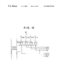
- FIG. 13 is a block diagram illustrating a configuration of a solid-state image sensing apparatus according to a seventh embodiment of the present invention.
- FIG. 14 is a circuit diagram illustrating a main configuration of a pixel
- FIG. 15 is a timing chart showing operation timing according to the seventh embodiment of the present invention.
- FIG. 16 is a circuit diagram illustrating a main portion of a pixel according to an eighth embodiment of the present invention.
- FIG. 17 is a circuit diagram of a conventional solid-state image sensing apparatus
- FIG. 18 is a circuit diagram corresponding to a single pixel of the conventional solid-state image sensing apparatus shown in FIG. 17 ;
- FIG. 19 is a timing chart for explaining an operation of the conventional solid-state image sensing apparatus.
- FIG. 20 is a diagram of a sensor area of another conventional solid-state image sensing apparatus.
- FIG. 21 is a circuit diagram of a horizontal switch circuit of the conventional solid-state image sensing apparatus.
- FIG. 22 is a timing chart for explaining an operation of the conventional solid-state image sensing apparatus.
- FIG. 23 is an explanatory view for explaining a problem of the conventional solid-state image sensing apparatus.
- the solid-state image sensing apparatus provides photo-charge, generated by the photodiode D 1 in accordance with the quantity of light, to the MOS amplifier Q 2 via the MOS switch Q 1 , then turns on the MOS selector Q 3 to transfer the photo-charge to a vertical signal line VL 3 .
- the signals ⁇ CR 1 , ⁇ CR 2 and ⁇ CS 1 at time t 1 are changed to high, thereby a MOS switch Q 16 is turned on; in turn, the vertical signal line VL 3 becomes a ground level, and the capacitors C 1 and C 3 are reset to the voltage VSS.
- the signal ⁇ CR 1 is changed to a low level at time t 2
- the reset signal ⁇ RS is changed to a high level, thereby the gate of the MOS amplifier Q 2 is reset to the voltage VRS.
- the reset signal ⁇ RS is changed to a low level and the signal ⁇ V 3 is changed to high, thereby the MOS selector Q 3 is turned on, and the operation voltage VDD is provided to the drain of the MOS amplifier Q 2 . Accordingly, a voltage VN corresponding to the gate voltage of the MOS amplifier Q 2 appears on the vertical signal line VL 3 (noise signal).
- the signal ⁇ CR 2 is changed to low at time t 4 , which puts the output side of the capacitor C 1 and one electrode of the capacitor C 3 in a floating state.
- the signal ⁇ V 3 is changed to low to turn the MOS selector Q 3 off.
- the signal ⁇ CR 1 is changed to high to reset the vertical signal line VL 3 , thereby the potential of the output side of the capacitor C 1 and one electrode of the capacitor C 3 becomes a potential, VSS ⁇ VN′, that is, the bias voltage VSS is reduced by a voltage VN′, which is a part of the voltage VN, corresponding to the ratio of the capacitance of the capacitor C 1 to the total capacitance of the capacitors C 1 and C 3 .
- the signal ⁇ VG applied to the gate of the MOS switch Q 1 is changed to high, and photo-charge is transferred from the photodiode D 1 to the gate of the MOS amplifier Q 2 .
- the signal ⁇ CR 1 is kept high to fix the source of the MOS amplifier Q 2 to a ground level, and the signal ⁇ V 3 is set to low to cut the supply of the voltage VDD to the drain of the MOS amplifier Q 2 , thereby it is possible to restrain the operational range of the MOS amplifier Q 2 to the triode region.
- a potential at the drain of the MOS amplifier Q 2 decreases to near the ground level, thereby a bias relationship between the gate and the drain of the MOS amplifier Q 2 , namely a potential difference between the gate and the drain of the MOS amplifier Q 2 is greater than a threshold, is maintained.
- the signal ⁇ VG is changed to low at time t 6 , then, the signal ⁇ CR 1 is changed to low and the signal ⁇ V 3 is changed to high at time t 7 , a voltage VS corresponding to the photo-charge transferred to the gate of the MOS amplifier Q 2 appears on the vertical signal line VL 3 (photo-charge signal). Accordingly, the potential at the output side of the capacitor C 1 and one electrode of the capacitor C 3 becomes (VSS ⁇ VN′+VS′).
- charge which can be dealt with in the linear operation region i.e., maximum allowable charge
- the gate capacitance of the MOS amplifier, while transferring the charge is increased, and the maximum allowable charge is increased by 15%, although there is no difference in the noise removal rate of fixed pattern noise between the conventional method and the method of the present invention.
- transference of a photo-charge signal from a photodiode of a photoelectric conversion element to the gate of a field effect transistor (FET) which functions as an amplifier is performed under a condition that the channel is formed under the gate of the FET by the reset voltage VRS, and the gate voltage is lowered by the transferred charge. Accordingly, a voltage corresponding to the lowered gate voltage appears on a vertical signal line.
- FET field effect transistor
- the gate voltage of the FET is higher than the sum of the source voltage and the threshold voltage of the FET.
- Each pixel includes a photodiode 1 , a transfer switch 2 , a reset switch 3 , a pixel amplifier 4 , and a row selection switch 5 and a plurality of such pixels are connected as shown in FIG. 3 .
- a source follower configured with a source of load current 7 and the pixel amplifier 4 , starts operating, and signals of a selected row are transferred to respective vertical output lines 6 .
- the signals are stored in signal storage unit 11 via respective transfer gates 8 .
- the signals, temporarily stored in the signal storage unit 11 are sequentially transferred to an output unit (not shown) via a horizontal scan circuit 12 .
- a signal ⁇ RES becomes high at t 21
- the gate of the pixel amplifier 4 is reset to a reset potential (potential of pulse ⁇ RES minus threshold potential).
- a signal ⁇ SEL becomes high at time t 22
- the source follower configured with the pixel amplifier 4 and the source of load current 7 , starts operating. Accordingly, noise corresponding to the reset potential appears on the corresponding vertical output line 6 , and is temporarily stored in the signal storage unit 11 by changing a signal ⁇ TN to high as well as turning a transfer gate 13 on.
- the signals ⁇ SEL and ⁇ TN are changed to low at time t 23 , and the potential of the vertical output line 6 decreases as load current is supplied from the source of current 7 .
- a transfer signal ⁇ TX becomes high at time t 24 , and photo-charge is transferred from each photodiode 1 to the gate of the pixel amplifier 4 .
- the pixel amplifier 4 operates in the triode region. Therefore, the gate capacitance of the pixel amplifier becomes the maximum. Thereafter, the signal ⁇ TX is changed to low at time t 251 then the signals ⁇ SEL and ⁇ TS are changed to high at time t 26 , and the photo-charge are read out.
- Each pixel includes a photodiode 1 , a transfer switch 2 , a reset switch 3 , a pixel amplifier 4 , and a row selection switch 5 and a plurality of such pixels are connected as shown in FIG. 5 .
- a source follower configured with a source of load current 7 and the pixel amplifier 4 , starts operating, and signals of a selected row are transferred to respective vertical output lines 6 .
- the signals are stored in signal storage unit 11 via respective transfer gates 8 .
- the signals are sequentially transferred to an output unit (not shown) via a horizontal scan circuit 12 .
- vertical-output-line reset switches 9 for resetting the vertical output lines 6 to a fixed potential are also provided. Differences between FIG. 5 and FIG. 3 are that the vertical-output-line reset switches 9 are provided and a reset pulse ⁇ VR is supplied to the gate of the reset switches 9 in FIG. 5 .
- the signal ⁇ VR becomes high at t 31 , and the vertical output lines 6 are reset to a fixed potential (ground potential in the third embodiment).
- a signal ⁇ RES becomes high at t 33 , then the gate of the pixel amplifier 4 is reset to a reset potential.
- the signal ⁇ RES is changed to low, and signals ⁇ SEL and ⁇ TN become high at time t 34 .
- the source follower configured with the pixel amplifier 4 and the source of load current 7 , starts operating, and noise corresponding to the reset potential appears on the corresponding vertical output line 6 , and is temporarily stored in the signal storage unit 11 by turning on the transfer gate 13 .
- the signal ⁇ VR becomes high at time t 36 , and the vertical output lines 6 are again reset to the ground potential.
- the transfer signal ⁇ TX becomes high at time t 37 , in turn, photo-charge is transferred from the photodiode 1 to the gate of the pixel amplifier 4 .
- the source of the pixel amplifier (MOS FET) 4 is fixed to the ground potential to which the vertical output lines 6 are reset. Further, since the drain of the pixel amplifier 4 is not supplied with a voltage, the operation of the pixel amplifier 4 is limited to the triode region.
- the signals ⁇ SEL and ⁇ TS are changed to high at time t 39 , and the photo-charge is transferred to the corresponding vertical output line 6 , further, read out to the signal storage unit 11 by turning on the transfer gate 8 .
- the vertical output lines 6 can be reset, therefore, there is no such limitation as described above associated with the configuration of the photoelectric conversion element as described in the second embodiment.
- the potential of the vertical output line 6 changes while the gate potential of the pixel amplifier 4 is in the floating state, a feed-back phenomenon is caused by gate-source capacitance of the pixel amplifier 4 .
- the potential of the vertical output line 6 always increases from the ground potential, the ratio of the feed-back voltage to the voltage of the photo-charge is kept constant, and the photo-charge output is kept linear as an additional effect.
- the maximum allowable charge Qsat is increased by 13% according to the third embodiment, since the gate capacitance of the pixel amplifier 4 is maximum when transferring photo-charge to the gate of the pixel amplifier 4 .
- Each pixel includes a photodiode 1 , a transfer switch 2 , a reset switch 3 , a pixel amplifier 4 , and a row selection switch 5 and a plurality of such pixels are connected as shown in FIG. 7 .
- the pixel amplifier 4 is connected to a corresponding vertical output line 6 via the row selection switch 5 , and when the pixel amplifier 4 and the row selection switch 5 are turned on the pixel amplifier 4 , with a resistor 47 , operates as an inverse amplifier.
- vertical-output-line reset switches 9 for resetting the vertical output lines 6 to a fixed potential (ground potential in the fourth embodiment) are also provided.
- the pixel amplifier 4 in FIG. 7 differs from the pixel amplifier 4 in FIG. 5 in that it operates as an inverse amplifier with the resistor 47 .
- a signal ⁇ RES becomes high at t 41
- the gate of the pixel amplifier 4 is reset to a reset potential.
- signals ⁇ SEL and ⁇ TN become high at time t 42
- the transfer gate 13 is turned on, and noise is read out.
- a signal ⁇ VR is changed to high at time t 44 , and the vertical output line 6 and the drain of the pixel amplifier 4 are reset to the ground potential.
- the signals ⁇ SEL and ⁇ VR are changed to low at time t 45 , accordingly, the drain of the pixel amplifier 4 is put into the floating state while maintaining the ground potential. At this time, the source of the pixel amplifier 4 is grounded, thus, the operation of the pixel amplifier 4 is limited to the triode region.
- a signal ⁇ TX becomes high at time t 46 , and photo-charge is transferred from the photodiode 1 to the gate of the pixel amplifier 4 .
- the signal ⁇ TX is changed to low at time t 47 , the row selection signal ⁇ SEL and the signal ⁇ TS are changed to high at time t 48 .
- the transfer gates 8 are turned on and the photo-charge signals are read out.
- the noise signals and the photo-charge signals stored in a signal storage unit 11 are sequentially outputted via a horizontal scan circuit 12 in accordance with a horizontal scan signal ⁇ H( 1 , 2 ).
- the pixel amplifier 4 is in the triode state while transferring photo-charge to the gate of the pixel amplifier 4 , and the maximum allowable charge Qsat is increased by 25% comparing to the conventional operation method.
- Each pixel includes a photodiode 1 , a transfer switch 2 , a reset switch 3 , a pixel amplifier 4 , and a row selection switch 5 and a plurality of such pixels are connected as shown in FIG. 9 .
- a source follower configured with a source of load current 7 and the pixel amplifier 4 , starts operating, and signals of a selected row are transferred to respective vertical output lines 6 .
- the signals are stored in signal storage unit 11 via respective transfer gates 8 .
- the signals are sequentially transferred to an output unit (not shown) via a horizontal scan circuit 12 .
- vertical-output-line reset switches 9 for resetting the vertical output lines 6 to a fixed potential are also provided. Differences between FIG. 9 and FIG. 5 are that the row selection switch 5 is connected in the side of the source of the pixel amplifier 4 , and a noise signal and a photo-charge signal are both read out to the corresponding vertical output line 6 via the row selection switch 5 .
- a signal ⁇ RES becomes high at t 51 , then the gate of the pixel amplifier 4 is reset to a reset potential. Thereafter, signals ⁇ SEL and ⁇ TN become high at time t 52 , and noise is read out to the signal storage unit 11 . After reading the noise signal, the signal ⁇ TN is changed to low at time t 53 and a signal ⁇ VR is changed to high at time t 54 , thereby the vertical output line 6 is reset. At this time, since the signal ⁇ SEL is kept high, the potential at the source of the pixel amplifier 4 is simultaneously reset and fixed to the ground potential.
- the signal ⁇ TX becomes high at time t 55 , and photo-charge is transferred from the photodiode 1 to the gate of the pixel amplifier 4 .
- the gate potential of the pixel amplifier 4 decreases; however, since the source of the pixel amplifier 4 is fixed to the ground potential through the row selection switch 5 , the pixel amplifier 4 is always in the on-state during transferring the photo-charge.
- the signals ⁇ VR and ⁇ TX are changed to low at time t 56 and a signal ⁇ TS is changed to high at time t 57 , thereby the photo-charge signal is read out to the signal storage unit 11 .
- the signals ⁇ SEL and ⁇ TS are changed to low to finish reading operation of one row, and the process proceeds to operation of reading the next row.
- the maximum allowable charge Qsat is increased by 43% comparing to the conventional operation method.
- the solid-state image sensing apparatus has a vertical-output-line reset switches 9 , however, they may be omitted if the sources of load current 7 supply sufficiently large current and the source of the pixel amplifiers 4 are quickly decreased to the ground potential before transferring photo-charges to the gate of the pixel amplifiers 4 .
- Each pixel includes a photodiode 1 , a transfer switch 2 , a reset switch 3 , a pixel amplifier 4 , and a row selection switch 5 and a plurality of such pixels are connected as shown in FIG. 11 , similarly to FIG. 9 . Note, only four pixels are shown in FIG. 11 , however, a number of pixels are arranged in practice.
- a source follower configured with a source of load current 7 and the pixel amplifier 4 , starts operating, and signals of a selected row are transferred to respective vertical output line 6 .
- the signals are stored in signal storage unit 11 via respective transfer gates 8 , 14 , 15 , or 16 .
- the signals, temporarily stored in the signal storage unit 11 are sequentially transferred to an output unit via a horizontal scan circuit 12 .
- vertical-output-line reset switches 9 for resetting the vertical output lines 6 to a fixed potential are also provided.
- signals in the even-number rows and signals in the odd-number rows are separately transferred to the signal storage unit 11 using the transfer gates 8 , 14 , 15 and 16 . Accordingly, it is possible to read out signals of two rows during horizontal blanking period.
- FIG. 12 is a view showing a configuration of a part of a vertical scan circuit 10 of the solid-state image sensing apparatus shown in FIG. 11 .
- a signal ⁇ SEL 1 for selecting the odd-number rows and a signal ⁇ SEL 2 for selecting the even-number rows which are independently provided signals of two rows are transferred to the signal storage unit 11 in the single horizontal blanking period.
- the vertical scan circuit 10 includes a vertical shift register 17 which outputs a pulse signal V(n) for selecting a n-th pair of adjoining odd- and even-number rows, and plural sets of NOR gates 18 to 21 , each pair corresponds to each even-and-odd-number-row pair.
- the NOR gates 18 to 21 When the pulse signal V(n), selecting the n-th pair of rows, is inputted, then the NOR gates 18 to 21 outputs selection signals ⁇ SEL 1 (n) and ⁇ SEL 2 (n) to the corresponding rows, and a reset signal ⁇ RES (n) and a transfer signal ⁇ TX(n) to both of the even and rows of the n-th pair for operating the respective pixels.
- the signals ⁇ SEL 1 and ⁇ TN 1 becomes high at time t 61 , and noise in the odd-number row is read out to the signal storage unit 11 .
- the signals ⁇ SEL 1 and ⁇ TN 1 are changed to low at time t 62 , and the signals ⁇ SEL 2 and ⁇ TN 2 are changed to high at time t 63 , and noise in the even-number row is read out to the signal storage unit 11 by the time t 64 .
- the reset potential is the ground potential.
- a signal ⁇ TX is changed to high, and photo-charge is transferred from the photodiode 1 to the gate of the pixel amplifier 4 .
- the gate potential of the pixel amplifier 4 decreases, however, since the signals ⁇ SEL 1 and ⁇ SEL 2 are high and the row selection switch 5 is on, the source of the pixel amplifier 4 is fixed to the ground voltage through the row selection switch 5 and the pixel amplifier 4 is always in the on-state during transferring the photo-charge.
- Photo-charges in an odd-number row and an even-number row are read out to the signal storage units 11 by sequentially changing the signals ⁇ SEL 1 and ⁇ TS 1 , and ⁇ SEL 2 and ⁇ TS 2 to high (at times t 67 , t 68 , t 69 , t 70 ).
- photo-charge signals are sequentially read out for a frame image.
- the pixel amplifier 4 since the source of the pixel amplifier 4 is in the floating state while transferring photo-charge to the gate of the pixel amplifier 4 , the pixel amplifier 4 is turned off when large photo-charge is transferred. In contrast, the pixel amplifier 4 is fixed to the on-state in the sixth embodiment, the maximum allowable charge Qsat is increased by 45% comparing to the conventional operation method.
- photo-charge is transferred to the gate of a MOS transistor, used as the pixel amplifier 4 , in the optimum operation region of the MOS transistor by supplying operation pulses in various ways, the MOS transistor operates in the triode region where the MOS transistor operates linearly, thereby it is possible to read out the photo-charge while widening a dynamic range of the pixel amplifier 4 .
- the foregoing embodiments can be generally applied to any type of solid-state image sensing apparatus having a photoelectric conversion element, a field effect transistor whose gate receives photo-charge, and a transfer switch for controlling the connection between the photoelectric conversion element and the gate of the field effect transistor in each pixel unit, and the maximum allowable charge Qsat which can be dealt with by a source-follower type amplifier and the field effect transistor for inverse amplification is increased, thereby the dynamic range is widened. Accordingly, high-quality image signals of high S/N ratio can be obtained.
- FIG. 13 is a block diagram illustrating a configuration of a solid-state image sensing apparatus according to the seventh embodiment
- FIG. 14 is a circuit diagram illustrating a basic configuration of a pixel.
- a plurality of such pixels are formed on a single semiconductor substrate made of, e.g., mono-crystalline silicone, in CMOS LSI processing in accordance with a manufacturing technique of a semi-conductor integrated circuit, and collectively called as “CMOS sensor” in general.
- CMOS sensor a manufacturing technique of a semi-conductor integrated circuit
- each of the pixels S 11 to Smn is explained with reference to FIG. 14 .
- the anode of a photodiode PD which generates photo-charge is grounded in the seventh embodiment.
- the cathode of the photodiode PD is connected to the gate of a MOS transistor M 3 for amplification (referred to as “MOS amplifier” hereinafter) via a charge transfer switch TX.
- MOS amplifier MOS amplifier
- the source of a MOS transistor M 1 (referred to as “reset MOS” hereinafter) for resetting the MOS amplifier M 3 is connected.
- a reset voltage VR is provided to the drain of the reset MOS M 1 .
- the drain of the MOS amplifier M 3 is connected to a MOS transistor M 2 (referred to as “MOS selector” hereinafter) to select a row to which an operation voltage VDD is applied.
- the gates of charge transfer switches TX of the pixels S 11 to Smn are connected to first row selection lines (vertical scan lines) TX 1 to TXm each extending in the horizontal direction.
- first row selection lines vertical scan lines
- the gates of charge transfer switches TX of pixels S 11 to S 1 n in the first row are connected to the first row selection line TX 1
- the gates of charge transfer switches TX of pixels Si 1 to Sin (i is an arbitrary integer) in the i-th row are connected to the first row selection line TXi.
- the gates of the MOS transistors M 1 of the pixels S 11 to S 1 n are connected to a second row selection line (vertical scan line) RES 1 which also extends in the horizontal direction.
- the gates of MOS transistors M 1 of pixels Si 1 to Sin in the 1-th row are connected to the second row selection line RESi.
- the gates of the MOS transistors M 3 of the pixels S 11 to S 1 n are connected to a third row selection line (vertical scan line) SEL 1 which also extends in the horizontal direction.
- the gates of MOS transistors M 3 of pixels Si 1 to Sin in the i-th row are connected to the third row selection line SELi.
- These first to third row selection lines TXi, RESi, and SELi are connected to a vertical scan circuit 71 , and applied with voltage signals in accordance with the following operation timing shown in FIG. 15 .
- signals ⁇ TX 1 to ⁇ TXM, ⁇ RES 1 to ⁇ RESm, and ⁇ SEL 1 to ⁇ SELm are provided from the vertical scan circuit 71 .
- the sources of the MOS transistors M 3 of the pixels S 11 to Sm 1 are connected to a vertical signal line V 1 which extends in the vertical direction.
- the sources of the MOS transistors M 3 of pixels S 1 j to Smj (j is an arbitrary integer) in the j-th column are connected to a vertical signal line Vj.
- the vertical signal line V 1 is connected to a constant current source I 1 which is a load, as well as applied with a vertical line reset voltage VVR via a MOS transistor M 8 , when it is on, for resetting the vertical signal line V 1 .
- the vertical signal line V 1 is connected to a capacitor CTN for temporarily storing a noise signal via a noise signal transfer switch M 4 , and to a capacitor CTS for temporarily storing a photo-charge signal via a photo-charge signal transfer switch M 5 .
- the other side of the capacitors CTN and CTS are grounded.
- a node VIN between the noise signal transfer switch M 4 and the capacitor CTN, and a node VIS between the photo-charge signal transfer switch M 5 and the capacitor CTS are provided with a voltage VRCT via capacitor reset switches M 9 and M 10 , respectively, when they are on, further, connected to a differential block 73 for taking the difference between the photo-charge signal and the noise signal via horizontal transfer switches M 6 and M 7 , respectively.
- the gates of the horizontal transfer switches M 6 and M 7 are both connected to a column selection line H 1 , further connected to a horizontal scan circuit 72 .
- the identical circuit for reading signals is configured.
- the gates of the vertical line reset switches M 8 , the noise signal transfer switches M 4 , and the photo-charge signal transfer switches M 5 which are provided for each of the vertical signal lines V 1 to Vn, are connected to lines VRES, TN, and TS, respectively, to which signals ⁇ VRES, ⁇ TN, and ⁇ TS are provided, respectively.
- the signal ⁇ RES 1 applied to the gates of the reset MOS M 1 in the first row, and the signal ⁇ VRES, applied to the gates of the MOS transistors M 8 , become high before time t 71 . Accordingly, the gates of the MOS amplifier M 3 are reset to the voltage VR, and the vertical signal lines V 1 to Vn are reset to the voltage VVR.
- the signal ⁇ RES 1 applied to the gates of the reset MOS M 1 , and the signal ⁇ VRES, applied to the gates of the MOS transistors M 8 , are changed to low at time t 71 , the signal ⁇ SEL 1 , applied to the gates of the MOS selectors M 2 in the first row, and the signal ⁇ TN applied to the gates of the noise signal transfer switches M 4 become high at time t 72 .
- the reset signal VR is superposed with a reset noise, and multiplied by a gain A by the MOS amplifiers M 3 , further shifted by a gate-source voltage VGS of the MOS amplifiers. Then, the resultant noise signals are read out to the respective capacitors CTN.
- VIN A ⁇ ( VR ⁇ VGS ) (6)
- VGS the gate-source voltage VGS varies depending upon a threshold voltage Vth of each MOS amplifier M 3 in each pixel, as described above.
- the voltages of the vertical signal lines V 1 to Vn gradually decrease as they are discharged at a time constant determined by parasitic capacitances CP of the vertical signal lines V 1 to Vn and the constant current sources (I 1 ). Since the constant current source (I 1 ) is connected to each vertical signal line, even though the voltage VVR for resetting the vertical signal lines V 1 to Vn is set to a substantially high voltage and the MOS amplifiers M 3 are in the off state at the start of reading signals, the voltages of the vertical signal lines V 1 to Vn decrease due to the constant current, and the MOS amplifiers M 3 are eventually turned on, thus the signals are read out. Therefore, there is no limitation on the level of reset voltage for the vertical signal lines V 1 to Vn.
- the signal ⁇ VRES, applied to the gates of the MOS transistors M 8 are changed to high at time t 74 , and the vertical signal lines V 1 to Vn are reset to the voltage VVR again. Accordingly, an initial voltage of the vertical signal lines V 1 to Vn for reading photo-charge is set to the same voltage as that for reading the noise signals. Therefore, when it is not possible to take a sufficient period since noise signals are read until photo-charges are transferred, an initial potential of the vertical signal line when outputting a noise signal and an initial potential of the vertical signal line when outputting a photo-charge signal are identical; therefore, noise reduction operation, which will be explained later, is performed at high precision.
- the signal ⁇ TXL applied to the gates of the charge transfer switches TX in the first row becomes high at time t 75 , and the photo-charge generated by the photodiode PD is transferred to the gates of the respective MOS amplifiers M 3 .
- the signals ⁇ SEL 1 , applied to the gates of the MOS selectors M 2 in the first row, and the signal ⁇ TS applied to the gates of the photo-charge signal transfer switches M 5 become high at time t 78 .
- the photo-charge signal (voltage) Vsig is amplified by the gain A of the corresponding MOS amplifier M 3 and shifted by a gate-source voltage of the MOS amplifier M 3 , and a resultant voltage is read out to the capacitor CTS.
- the output voltage V 1 S is expressed by the following equation (7).
- V 1 S A ⁇ ( Vsig ⁇ VGS ) (7)
- the signal ⁇ SEL 1 applied to the gates of the MOS selectors M 2 , and the signal ⁇ TS, applied to the gates of the photo-charge signal transfer switches M 5 , are changed to low at time t 79 .
- the voltages of the vertical signal lines V 1 to Vn gradually decrease as they are discharged at a time constant determined by parasitic capacitances Cp of the vertical signal lines V 1 to Vn and the constant current sources (I 1 ).
- the signal ⁇ VRES applied to the gates of the MOS transistors M 8 , becomes high at time t 710 , thereby the signal lines V 1 to Vn are reset.
- the noise signals and photo-charge signals of the pixels S 11 to S 1 n are stored in the capacitors CTN for storing noise signals and the capacitors CTS for storing photo-charge signals, each provided for the respective columns.
- the differential block 73 takes the differences between the photo-charge signals V 1 S to VnS and the corresponding noise signals V 1 N to VnN, and sequentially outputs the differences as a voltage VOUT.
- the output voltage VOUT of the first column is expressed by the following equation, obtained by subtracting equation (6) from equation (7).
- the seventh embodiment in reading a noise signal and a photo-charge signal to the capacitors CTN and CTS, a capacitive division configuration is not adopted; thus, the capacitances of the capacitors CTN and CTS are not affected by the parasitic capacitance of the vertical output lines, and a small-size solid-state image sensing apparatus as well as high speed reading of the solid-state image sensing apparatus are realized.
- FIG. 16 is a circuit diagram illustrating a basic configuration of a pixel according to the eighth embodiment of the present invention. Referring to FIG. 16 , the basic configuration of each pixel is explained. In FIG. 16 , units and elements as those shown in FIG. 14 are referred to by the same references, and a plurality of such pixels are arranged as shown in FIG. 13 . Pixels and peripheral circuits are manufactured in CMOS LSI processing, and collectively called as “CMOS sensor”.
- Photodiodes may be formed while forming a source-drain diffusion layer.
- the photodiodes in the pixels according to the eighth embodiment of the present invention are complete depletion type buried photodiodes, processes for forming the photodiodes are added to standard CMOS LSI processing. With the complete depletion type photodiodes, photo-charges of good linearity can be obtained.
- the anode of the photodiode PD which generates photo-charge is grounded.
- the cathode of the photodiode PD is connected to the gate of the MOS amplifier M 3 via the charge transfer switch TX.
- the source of the reset MOS M 1 for resetting the gate of the MOS amplifier M 3 is connected, and the drain of the reset MOS M 1 is applied with the reset voltage VR.
- the drain of the MOS amplifier M 3 is applied with the operation voltage VDD, and the source is connected to the MOS selector M 2 for connecting the MOS amplifier M 3 to the vertical signal line. Since the MOS selector M 2 is connected to the source of the MOS amplifier M 3 , it is possible to widen the dynamic range in the VDD side, compared against the pixel circuit shown in FIG. 14 .
- noise signals of the respective pixels are read-out in a period between time t 72 and time t 73 photo-charge signals are read out in a period between time t 78 and time t 79 , and the output signals VOUT, which are the differences between the photo-charge signals and the noise signals, are obtained by the differential block 73 .
- the output signals VOUT do not include components of threshold voltages Vth of the MOS transistors M 1 and M 3 , thus, fixed pattern noise of the CMOS sensor, which has been considered as a problem, is reduced.
- the both terms Vsig and VR in the right hand side of equation (8) include reset noise, therefore, the reset noise is canceled out.
- a component of the photo-charge generated by the photodiode PD is converted to a voltage, i.e., the output voltage VOUT. Therefore, noise due to variation in the threshold voltage of the amplifier is also reduced, thereby an image signal of high S/N ratio can be obtained.
- CMOS sensor including the vertical scan circuit and the horizontal scan circuit becomes possible, which enables to produce a small-sized image sensor consuming low electrical energy.
- a load for a MOS amplifier is provided and a signal is temporary stored in a capacitor via a source follower, thus, better sensitivity is achieved with a smaller capacitance of the capacitor than a clamping capacitor C 1 ( FIG. 17 ). Accordingly, the chip size of a solid-state image sensing apparatus can be reduced.
- a switch for resetting each vertical signal line is provided and, in advance of reading of a photo-charge signal after reading a noise signal, the vertical signal line is reset to a predetermined reset voltage.
- the reset voltage for resetting the vertical signal line is set relatively high and the MOS amplifier is in the off state in an early stage of reading a photo-charge signal
- the voltage of the vertical signal line decreases in response to the constant current of the load, and the MOS amplifier is eventually turned on. Accordingly, the photo-charge signal is read out. Therefore, there is no limitation on the reset voltage to be applied to the vertical signal line.
- each vertical signal line is reset before reading noise as well as before reading photo-charge, thus the vertical signal line is refreshed each time signals is read from a pixel. Accordingly, it is possible to restrict interference between adjoining pixels as well as prevent cross modulation and blooming.
- NMOS transistors are mainly used in the circuits, however, the present invention is not limited to this, and it is possible to use PMOS transistors in place of the NMOS transistors. Further, the field effect transistors are not limited to the MOS type.
Abstract
Description
VN′=
VS′=
Thus, a high S/N signal, from which irregularity in the thresholds Vth of a MOS FET for resetting and of a MOS amplifier is reduced, is obtained as seen in the second term, (VN−VS).
VSO′=(
Further, a signal voltage VSO″ when a signal on the signal output line B2 is read out is expressed by the following equation (5).
VSO″=(
VIN=A×(VR−VGS) (6)
Note, the gate-source voltage VGS varies depending upon a threshold voltage Vth of each MOS amplifier M3 in each pixel, as described above.
V 1 S=A×(Vsig−VGS) (7)
VOUT=V 1 S−V 1 N=A×(Vsig−VR) (8)
Claims (6)
Applications Claiming Priority (2)
| Application Number | Priority Date | Filing Date | Title |
|---|---|---|---|
| JP11561398A JP3667081B2 (en) | 1998-04-24 | 1998-04-24 | Solid-state imaging device and driving method thereof |
| JP16992498A JP3667094B2 (en) | 1998-06-17 | 1998-06-17 | Solid-state imaging device |
Publications (1)
| Publication Number | Publication Date |
|---|---|
| US6963372B1 true US6963372B1 (en) | 2005-11-08 |
Family
ID=26454101
Family Applications (1)
| Application Number | Title | Priority Date | Filing Date |
|---|---|---|---|
| US09/291,006 Expired - Fee Related US6963372B1 (en) | 1998-04-24 | 1999-04-14 | Solid-state image sensing apparatus and method of operating the same |
Country Status (3)
| Country | Link |
|---|---|
| US (1) | US6963372B1 (en) |
| EP (1) | EP0952730B1 (en) |
| DE (1) | DE69922730T2 (en) |
Cited By (22)
| Publication number | Priority date | Publication date | Assignee | Title |
|---|---|---|---|---|
| US20030184288A1 (en) * | 2000-09-19 | 2003-10-02 | Jacky Bouvier | Device for punctual measurement of a radiofrequency magnetic field with constant amplitude and frequency |
| US20050121519A1 (en) * | 2003-12-05 | 2005-06-09 | Canon Kabushiki Kaisha | Solid state image pickup device, method of driving solid state image pickup device, and camera using the solid state image pickup device |
| US20050128324A1 (en) * | 2003-12-12 | 2005-06-16 | Takafumi Kishi | Image sensing apparatus and method of controlling same |
| US20050168605A1 (en) * | 2004-01-29 | 2005-08-04 | Canon Kabushiki Kaisha | Photoelectric conversion device and image pickup system using the photoelectric conversion device |
| US20050174453A1 (en) * | 2000-08-03 | 2005-08-11 | Sony Corporation | Solid-state image pickup device and camera system |
| US20050243194A1 (en) * | 2004-04-30 | 2005-11-03 | Eastman Kodak Company | Low noise sample and hold circuit for image sensors |
| US20070013796A1 (en) * | 1998-01-30 | 2007-01-18 | Canon Kabushiki Kaisha | Color filter array and image pickup apparatus having a color filter array |
| US20070126904A1 (en) * | 2000-04-12 | 2007-06-07 | Semiconductor Energy Laboratory Co., Ltd. | Semiconductor device and method of driving the same |
| US20080049130A1 (en) * | 2006-08-28 | 2008-02-28 | Canon Kabushiki Kaisha | Photoelectric conversion device and image pickup device |
| US20080170147A1 (en) * | 2006-12-21 | 2008-07-17 | Stmicroelectronics S.A. | Pinned photodiode cmos image sensor with a low supply voltage |
| US20080192134A1 (en) * | 2005-02-07 | 2008-08-14 | Hamamatsu Photonics K.K. | Solid-State Image Pickup Device |
| US20080252761A1 (en) * | 2003-03-27 | 2008-10-16 | Canon Kabushiki Kaisha | Image pickup apparatus |
| US7456882B1 (en) * | 1999-07-27 | 2008-11-25 | Canon Kabushiki Kaisha | Image pickup device |
| US20090128659A1 (en) * | 2000-08-25 | 2009-05-21 | Canon Kabushiki Kaisha | Image pickup apparatus |
| US20090237544A1 (en) * | 2000-02-28 | 2009-09-24 | Canon Kabushiki Kaisha | Image pickup apparatus |
| US20090295974A1 (en) * | 1998-11-02 | 2009-12-03 | Canon Kabushiki Kaisha | Solid-state image pickup device and method of resetting the same |
| US20100289933A1 (en) * | 2008-03-14 | 2010-11-18 | Canon Kabushiki Kaisha | Image sensing device and imaging system |
| US8553120B2 (en) | 2001-07-12 | 2013-10-08 | Canon Kabushiki Kaisha | Solid state image pickup apparatus |
| US20130284892A1 (en) * | 2011-01-17 | 2013-10-31 | Hamamatsu Photonics K.K. | Solid-state imaging device |
| US20140312207A1 (en) * | 2013-04-18 | 2014-10-23 | Canon Kabushiki Kaisha | Solid-state imaging apparatus and imaging system |
| US9972656B2 (en) | 2011-12-02 | 2018-05-15 | Arnold & Richter Cine Technik Gmbh & Co. Betriebs Kg | Image sensor and method of reading out an image sensor |
| CN112437238A (en) * | 2019-08-26 | 2021-03-02 | 天津大学青岛海洋技术研究院 | Low-kTC noise three-dimensional image sensor phase-locked pixel structure |
Families Citing this family (2)
| Publication number | Priority date | Publication date | Assignee | Title |
|---|---|---|---|---|
| DE19917863C1 (en) | 1999-04-20 | 2001-01-25 | Fraunhofer Ges Forschung | Circuit for processing an analog signal and image sensor |
| JP4681767B2 (en) | 2001-07-17 | 2011-05-11 | キヤノン株式会社 | Imaging device and camera |
Citations (8)
| Publication number | Priority date | Publication date | Assignee | Title |
|---|---|---|---|---|
| JPS5848577A (en) | 1981-09-18 | 1983-03-22 | Semiconductor Res Found | Picture signal readout method for solid-state image pickup device |
| JPH0461573A (en) | 1990-06-29 | 1992-02-27 | Hitachi Ltd | Picture element amplification solid-state image pickup element |
| JPH0518309A (en) | 1991-07-12 | 1993-01-26 | Daihatsu Motor Co Ltd | Calibrator for detected value of temperature of water cooling engine |
| EP0665685A2 (en) | 1994-01-31 | 1995-08-02 | Sony Corporation | Solid-state imager having photo fets and storage capacitors |
| US5793423A (en) * | 1991-03-18 | 1998-08-11 | Sony Corporation | Solid state image sensing device |
| US5933189A (en) * | 1995-03-09 | 1999-08-03 | Nikon Corporation | Solid state image pickup apparatus |
| US6037577A (en) * | 1997-03-11 | 2000-03-14 | Kabushiki Kaisha Toshiba | Amplifying solid-state image pickup device and operating method of the same |
| US6538693B1 (en) * | 1996-01-24 | 2003-03-25 | Canon Kabushiki Kaisha | Photoelectric conversion apparatus having reset noise holding and removing units |
-
1999
- 1999-04-14 US US09/291,006 patent/US6963372B1/en not_active Expired - Fee Related
- 1999-04-21 EP EP99303078A patent/EP0952730B1/en not_active Expired - Lifetime
- 1999-04-21 DE DE69922730T patent/DE69922730T2/en not_active Expired - Lifetime
Patent Citations (10)
| Publication number | Priority date | Publication date | Assignee | Title |
|---|---|---|---|---|
| JPS5848577A (en) | 1981-09-18 | 1983-03-22 | Semiconductor Res Found | Picture signal readout method for solid-state image pickup device |
| JPH0461573A (en) | 1990-06-29 | 1992-02-27 | Hitachi Ltd | Picture element amplification solid-state image pickup element |
| US5793423A (en) * | 1991-03-18 | 1998-08-11 | Sony Corporation | Solid state image sensing device |
| JPH0518309A (en) | 1991-07-12 | 1993-01-26 | Daihatsu Motor Co Ltd | Calibrator for detected value of temperature of water cooling engine |
| EP0665685A2 (en) | 1994-01-31 | 1995-08-02 | Sony Corporation | Solid-state imager having photo fets and storage capacitors |
| US5808677A (en) | 1994-01-31 | 1998-09-15 | Sony Corporation | Solid-state imaging device having a reset switch for resetting potential of capacitor |
| US6037979A (en) | 1994-01-31 | 2000-03-14 | Sony Corporation | Solid-state imaging device having a reset switch for resetting potential of capacitor and vertical signal line |
| US5933189A (en) * | 1995-03-09 | 1999-08-03 | Nikon Corporation | Solid state image pickup apparatus |
| US6538693B1 (en) * | 1996-01-24 | 2003-03-25 | Canon Kabushiki Kaisha | Photoelectric conversion apparatus having reset noise holding and removing units |
| US6037577A (en) * | 1997-03-11 | 2000-03-14 | Kabushiki Kaisha Toshiba | Amplifying solid-state image pickup device and operating method of the same |
Cited By (62)
| Publication number | Priority date | Publication date | Assignee | Title |
|---|---|---|---|---|
| US20070013796A1 (en) * | 1998-01-30 | 2007-01-18 | Canon Kabushiki Kaisha | Color filter array and image pickup apparatus having a color filter array |
| US7724292B2 (en) | 1998-01-30 | 2010-05-25 | Canon Kabushiki Kaisha | Color filter array for a CMOS sensor for generating a color signal in an image pickup apparatus |
| US20090295974A1 (en) * | 1998-11-02 | 2009-12-03 | Canon Kabushiki Kaisha | Solid-state image pickup device and method of resetting the same |
| US8120682B2 (en) | 1998-11-02 | 2012-02-21 | Canon Kabushiki Kaisha | Solid-state image pickup device and method of resetting the same |
| US9083901B2 (en) | 1998-11-02 | 2015-07-14 | Canon Kabushiki Kaisha | Solid-state image pickup device and method of resetting the same |
| US7456882B1 (en) * | 1999-07-27 | 2008-11-25 | Canon Kabushiki Kaisha | Image pickup device |
| US20090237544A1 (en) * | 2000-02-28 | 2009-09-24 | Canon Kabushiki Kaisha | Image pickup apparatus |
| US8085330B2 (en) | 2000-02-28 | 2011-12-27 | Canon Kabushiki Kaisha | Image pickup apparatus |
| US8717475B2 (en) | 2000-02-28 | 2014-05-06 | Canon Kabushiki Kaisha | Image pickup apparatus |
| US9019408B2 (en) | 2000-04-12 | 2015-04-28 | Semiconductor Energy Laboratory Co., Ltd. | Semiconductor device and method of driving the same |
| US8743250B2 (en) | 2000-04-12 | 2014-06-03 | Semiconductor Energy Laboratory Co., Ltd. | Semiconductor device and method of driving the same |
| US20070126904A1 (en) * | 2000-04-12 | 2007-06-07 | Semiconductor Energy Laboratory Co., Ltd. | Semiconductor device and method of driving the same |
| US20110018041A1 (en) * | 2000-04-12 | 2011-01-27 | Semiconductor Energy Laboratory Co., Ltd. | Semiconductor Device and Method of Driving the Same |
| US7808535B2 (en) | 2000-04-12 | 2010-10-05 | Semiconductor Energy Laboratory Co., Ltd. | Semiconductor device and method of driving the same |
| US8355065B2 (en) | 2000-04-12 | 2013-01-15 | Semiconductor Energy Laboratory Co., Ltd. | Semiconductor device and method of driving the same |
| US8203636B2 (en) | 2000-04-12 | 2012-06-19 | Semiconductor Energy Laboratory Co., Ltd. | Semiconductor device and method of driving the same |
| US9568615B2 (en) | 2000-04-12 | 2017-02-14 | Semiconductor Energy Laboratory Co., Ltd. | Semiconductor device and method of driving the same |
| US9274236B2 (en) | 2000-04-12 | 2016-03-01 | Semiconductor Energy Laboratory Co., Ltd. | Semiconductor device and method of driving the same |
| US7545425B2 (en) * | 2000-08-03 | 2009-06-09 | Sony Corporation | Solid-state image pickup device and camera system |
| US20050174453A1 (en) * | 2000-08-03 | 2005-08-11 | Sony Corporation | Solid-state image pickup device and camera system |
| US7995127B2 (en) | 2000-08-25 | 2011-08-09 | Canon Kabushiki Kaisha | Pixel drive circuit for image pickup apparatus |
| US20090128659A1 (en) * | 2000-08-25 | 2009-05-21 | Canon Kabushiki Kaisha | Image pickup apparatus |
| US9088743B2 (en) | 2000-08-25 | 2015-07-21 | Canon Kabushiki Kaisha | Scanning circuit for image pickup apparatus |
| US7429859B2 (en) * | 2000-09-19 | 2008-09-30 | Fahrenheit Thermoscope Llc | Device for punctual measurement of a radiofrequency magnetic field with constant amplitude and frequency |
| US7573263B2 (en) | 2000-09-19 | 2009-08-11 | Fahrenheit Thermoscope Llc | Device for punctual measurement of a radiofrequency magnetic field with constant amplitude and frequency |
| US20030184288A1 (en) * | 2000-09-19 | 2003-10-02 | Jacky Bouvier | Device for punctual measurement of a radiofrequency magnetic field with constant amplitude and frequency |
| US20070126423A1 (en) * | 2000-09-19 | 2007-06-07 | Jacky Bouvier | Device for punctual measurement of a radiofrequency magnetic field with constant amplitude and frequency |
| US8553120B2 (en) | 2001-07-12 | 2013-10-08 | Canon Kabushiki Kaisha | Solid state image pickup apparatus |
| US9055211B2 (en) | 2001-07-12 | 2015-06-09 | Canon Kabushiki Kaisha | Image pickup apparatus |
| US20100259663A1 (en) * | 2003-03-27 | 2010-10-14 | Canon Kabushiki Kaisha | Image pickup apparatus |
| US20080252761A1 (en) * | 2003-03-27 | 2008-10-16 | Canon Kabushiki Kaisha | Image pickup apparatus |
| US20100045839A1 (en) * | 2003-03-27 | 2010-02-25 | Canon Kabushiki Kaisha | Image pickup apparatus |
| US7924336B2 (en) | 2003-03-27 | 2011-04-12 | Canon Kabushiki Kaisha | Image pickup apparatus including a driving circuit to control a clamping switch so as to hold signals in holding capacitors |
| US8081250B2 (en) | 2003-03-27 | 2011-12-20 | Canon Kabushiki Kaisha | Image pickup apparatus having a correction unit for correction of noise components generated by clamping circuits |
| US7633541B2 (en) | 2003-03-27 | 2009-12-15 | Canon Kabushiki Kaisha | Image pickup apparatus having a correction unit for a digital image signal |
| US8610811B2 (en) | 2003-03-27 | 2013-12-17 | Canon Kabushiki Kaisha | Image pickup apparatus |
| US20050121519A1 (en) * | 2003-12-05 | 2005-06-09 | Canon Kabushiki Kaisha | Solid state image pickup device, method of driving solid state image pickup device, and camera using the solid state image pickup device |
| US7394492B2 (en) | 2003-12-05 | 2008-07-01 | Canon Kabushiki Kaisha | Solid state image pickup device, method of driving solid state image pickup device, and camera using the solid state image pickup device |
| US20050128324A1 (en) * | 2003-12-12 | 2005-06-16 | Takafumi Kishi | Image sensing apparatus and method of controlling same |
| US7675559B2 (en) * | 2003-12-12 | 2010-03-09 | Canon Kabushiki Kaisha | Image sensing apparatus having a two step transfer operation and method of controlling same |
| US20050168605A1 (en) * | 2004-01-29 | 2005-08-04 | Canon Kabushiki Kaisha | Photoelectric conversion device and image pickup system using the photoelectric conversion device |
| US20090102955A1 (en) * | 2004-01-29 | 2009-04-23 | Canon Kabushiki Kaisha | Photoelectric conversion device and image pickup system using the photoelectric conversion device |
| US7852390B2 (en) | 2004-01-29 | 2010-12-14 | Canon Kabushiki Kaisha | Photoelectric conversion device and image pickup system using the photoelectric conversion device |
| US8159581B2 (en) | 2004-01-29 | 2012-04-17 | Canon Kabushiki Kaisha | Photoelectric conversion device and image pickup system using the photoelectric conversion device |
| US7486320B2 (en) | 2004-01-29 | 2009-02-03 | Canon Kabushiki Kaisha | Photoelectric conversion device and image pickup system using the photoelectric conversion device |
| US7385636B2 (en) * | 2004-04-30 | 2008-06-10 | Eastman Kodak Company | Low noise sample and hold circuit for image sensors |
| US20050243194A1 (en) * | 2004-04-30 | 2005-11-03 | Eastman Kodak Company | Low noise sample and hold circuit for image sensors |
| US20080192134A1 (en) * | 2005-02-07 | 2008-08-14 | Hamamatsu Photonics K.K. | Solid-State Image Pickup Device |
| US8018515B2 (en) * | 2005-02-07 | 2011-09-13 | Hamamatsu Photonics K.K. | Solid-state image pickup device |
| US7639305B2 (en) | 2006-08-28 | 2009-12-29 | Canon Kabushiki Kaisha | Photoelectric conversion device and image pickup device |
| US20080049130A1 (en) * | 2006-08-28 | 2008-02-28 | Canon Kabushiki Kaisha | Photoelectric conversion device and image pickup device |
| US20080170147A1 (en) * | 2006-12-21 | 2008-07-17 | Stmicroelectronics S.A. | Pinned photodiode cmos image sensor with a low supply voltage |
| US8284280B2 (en) * | 2006-12-21 | 2012-10-09 | Stmicroelectronics S.A. | Pinned photodiode CMOS image sensor with a low supply voltage |
| US9191597B2 (en) | 2006-12-21 | 2015-11-17 | Stmicroelectronics S.A. | Pinned photodiode CMOS image sensor with a low supply voltage |
| US20100289933A1 (en) * | 2008-03-14 | 2010-11-18 | Canon Kabushiki Kaisha | Image sensing device and imaging system |
| US8368785B2 (en) | 2008-03-14 | 2013-02-05 | Canon Kabushiki Kaisha | Image sensing device and imaging system |
| US9369643B2 (en) * | 2011-01-17 | 2016-06-14 | Hamamatsu Photonics K.K. | Solid-state imaging device |
| US20130284892A1 (en) * | 2011-01-17 | 2013-10-31 | Hamamatsu Photonics K.K. | Solid-state imaging device |
| US9972656B2 (en) | 2011-12-02 | 2018-05-15 | Arnold & Richter Cine Technik Gmbh & Co. Betriebs Kg | Image sensor and method of reading out an image sensor |
| US20140312207A1 (en) * | 2013-04-18 | 2014-10-23 | Canon Kabushiki Kaisha | Solid-state imaging apparatus and imaging system |
| US9942497B2 (en) * | 2013-04-18 | 2018-04-10 | Canon Kabushiki Kaisha | Solid-state imaging apparatus and imaging with a limiting circuit for limiting an amplifier output in first and second periods to first and second ranges |
| CN112437238A (en) * | 2019-08-26 | 2021-03-02 | 天津大学青岛海洋技术研究院 | Low-kTC noise three-dimensional image sensor phase-locked pixel structure |
Also Published As
| Publication number | Publication date |
|---|---|
| EP0952730A3 (en) | 2000-11-08 |
| DE69922730D1 (en) | 2005-01-27 |
| EP0952730B1 (en) | 2004-12-22 |
| DE69922730T2 (en) | 2005-12-15 |
| EP0952730A2 (en) | 1999-10-27 |
Similar Documents
| Publication | Publication Date | Title |
|---|---|---|
| US6963372B1 (en) | Solid-state image sensing apparatus and method of operating the same | |
| US10171760B2 (en) | Solid-state imaging device, method for driving solid-state imaging device, and electronic apparatus using an amplifier and signal lines for low and high gain | |
| US7692702B2 (en) | Solid-state imaging device with amplifiers corresponding to signal lines and alternating control voltage | |
| US7292276B2 (en) | High-speed solid-state imaging device capable of suppressing image noise | |
| US8624308B2 (en) | Image sensor five transistor pixel element with four control signals | |
| US20160127666A1 (en) | Solid-state imaging element having image signal overflow path | |
| US7399951B2 (en) | Solid-state image-sensing device | |
| US20080237446A1 (en) | Solid-state image pickup device and method | |
| KR101900668B1 (en) | Solid-state imaging element, and imaging device | |
| JP3667094B2 (en) | Solid-state imaging device | |
| US8159586B2 (en) | Solid-state imaging apparatus | |
| US8294798B2 (en) | Solid-state imaging apparatus | |
| US6697114B1 (en) | Triple slope pixel sensor and arry | |
| US6822211B2 (en) | Solid-state image-sensing device | |
| KR20060112223A (en) | Solid state imaging device, method of driving solid state imaging device and image pickup apparatus | |
| JP2008305983A (en) | Solid-state imaging element | |
| US20090046187A1 (en) | Solid-state imaging device | |
| US8319873B2 (en) | Solid-state imaging device | |
| JP4746962B2 (en) | Solid-state imaging device and imaging system | |
| JP3487575B2 (en) | Photoelectric conversion device | |
| Hoekstra et al. | Memory read-out approach for a 0.5-um CMOS image sensor | |
| JP2001197378A (en) | Solid-state image pickup element | |
| US20060232693A1 (en) | Imaging device and digital camera |
Legal Events
| Date | Code | Title | Description |
|---|---|---|---|
| AS | Assignment |
Owner name: CANON KABUSHIKI KAISHA, JAPAN Free format text: ASSIGNMENT OF ASSIGNORS INTEREST;ASSIGNORS:HIYAMA, HIROKI;SUGAWA, SHIGETOSHI;UENO, ISAMU;AND OTHERS;REEL/FRAME:009897/0753;SIGNING DATES FROM 19990402 TO 19990408 |
|
| CC | Certificate of correction | ||
| FPAY | Fee payment |
Year of fee payment: 4 |
|
| FPAY | Fee payment |
Year of fee payment: 8 |
|
| REMI | Maintenance fee reminder mailed | ||
| LAPS | Lapse for failure to pay maintenance fees |
Free format text: PATENT EXPIRED FOR FAILURE TO PAY MAINTENANCE FEES (ORIGINAL EVENT CODE: EXP.) |
|
| STCH | Information on status: patent discontinuation |
Free format text: PATENT EXPIRED DUE TO NONPAYMENT OF MAINTENANCE FEES UNDER 37 CFR 1.362 |
|
| FP | Lapsed due to failure to pay maintenance fee |
Effective date: 20171108 |