US6975978B1 - Method and apparatus for fault simulation of semiconductor integrated circuit - Google Patents
Method and apparatus for fault simulation of semiconductor integrated circuit Download PDFInfo
- Publication number
- US6975978B1 US6975978B1 US09/699,077 US69907700A US6975978B1 US 6975978 B1 US6975978 B1 US 6975978B1 US 69907700 A US69907700 A US 69907700A US 6975978 B1 US6975978 B1 US 6975978B1
- Authority
- US
- United States
- Prior art keywords
- fault
- logic
- test pattern
- sequence
- power supply
- Prior art date
- Legal status (The legal status is an assumption and is not a legal conclusion. Google has not performed a legal analysis and makes no representation as to the accuracy of the status listed.)
- Expired - Fee Related, expires
Links
- 238000004088 simulation Methods 0.000 title claims abstract description 78
- 238000000034 method Methods 0.000 title claims description 111
- 239000004065 semiconductor Substances 0.000 title claims description 66
- 238000012360 testing method Methods 0.000 claims abstract description 354
- 230000001052 transient effect Effects 0.000 claims abstract description 153
- 108010076504 Protein Sorting Signals Proteins 0.000 claims description 3
- 230000007704 transition Effects 0.000 description 65
- 230000008859 change Effects 0.000 description 23
- 230000005856 abnormality Effects 0.000 description 18
- 230000015654 memory Effects 0.000 description 15
- 230000004044 response Effects 0.000 description 15
- 238000010586 diagram Methods 0.000 description 13
- 230000000630 rising effect Effects 0.000 description 10
- 230000003071 parasitic effect Effects 0.000 description 7
- 239000000872 buffer Substances 0.000 description 5
- 238000001514 detection method Methods 0.000 description 5
- 230000008569 process Effects 0.000 description 4
- 238000012545 processing Methods 0.000 description 4
- 230000007423 decrease Effects 0.000 description 3
- 230000006870 function Effects 0.000 description 3
- 238000010276 construction Methods 0.000 description 2
- 230000003111 delayed effect Effects 0.000 description 2
- 230000001419 dependent effect Effects 0.000 description 2
- 230000000694 effects Effects 0.000 description 2
- 238000007562 laser obscuration time method Methods 0.000 description 2
- 238000004519 manufacturing process Methods 0.000 description 2
- 239000002184 metal Substances 0.000 description 2
- 229910052751 metal Inorganic materials 0.000 description 2
- 230000000644 propagated effect Effects 0.000 description 2
- 238000003860 storage Methods 0.000 description 2
- 238000012546 transfer Methods 0.000 description 2
- 230000005641 tunneling Effects 0.000 description 2
- 235000001537 Ribes X gardonianum Nutrition 0.000 description 1
- 235000001535 Ribes X utile Nutrition 0.000 description 1
- 235000016919 Ribes petraeum Nutrition 0.000 description 1
- 244000281247 Ribes rubrum Species 0.000 description 1
- 235000002355 Ribes spicatum Nutrition 0.000 description 1
- 230000002159 abnormal effect Effects 0.000 description 1
- 230000004913 activation Effects 0.000 description 1
- 230000006399 behavior Effects 0.000 description 1
- 238000004364 calculation method Methods 0.000 description 1
- 230000000052 comparative effect Effects 0.000 description 1
- 230000003247 decreasing effect Effects 0.000 description 1
- 238000009792 diffusion process Methods 0.000 description 1
- 238000007599 discharging Methods 0.000 description 1
- 238000009826 distribution Methods 0.000 description 1
- 238000005530 etching Methods 0.000 description 1
- 230000000873 masking effect Effects 0.000 description 1
- 238000012986 modification Methods 0.000 description 1
- 230000004048 modification Effects 0.000 description 1
- 238000000059 patterning Methods 0.000 description 1
- 229910021420 polycrystalline silicon Inorganic materials 0.000 description 1
- 230000035945 sensitivity Effects 0.000 description 1
Images


Classifications
-
- G—PHYSICS
- G01—MEASURING; TESTING
- G01R—MEASURING ELECTRIC VARIABLES; MEASURING MAGNETIC VARIABLES
- G01R31/00—Arrangements for testing electric properties; Arrangements for locating electric faults; Arrangements for electrical testing characterised by what is being tested not provided for elsewhere
- G01R31/28—Testing of electronic circuits, e.g. by signal tracer
- G01R31/317—Testing of digital circuits
- G01R31/3181—Functional testing
- G01R31/3183—Generation of test inputs, e.g. test vectors, patterns or sequences
- G01R31/318342—Generation of test inputs, e.g. test vectors, patterns or sequences by preliminary fault modelling, e.g. analysis, simulation
-
- G—PHYSICS
- G01—MEASURING; TESTING
- G01R—MEASURING ELECTRIC VARIABLES; MEASURING MAGNETIC VARIABLES
- G01R31/00—Arrangements for testing electric properties; Arrangements for locating electric faults; Arrangements for electrical testing characterised by what is being tested not provided for elsewhere
- G01R31/28—Testing of electronic circuits, e.g. by signal tracer
- G01R31/30—Marginal testing, e.g. by varying supply voltage
- G01R31/3004—Current or voltage test
Definitions
- the present invention relates to a fault simulation method and apparatus which make a list of faults in a semiconductor integrated circuit that are detectable using a certain test pattern sequence.
- a semiconductor integrated circuit hereinafter referred to as a semiconductor IC or simply as an IC
- predetermined test patterns are input to the semiconductor IC with faults assumed to lie therein, then response output values available from its output terminal are calculated by a logic simulation to detect variations in the output values relative to those obtainable under fault-free conditions, and the results thus obtained are summarized as a comparative table of assumed faults and input/output logic values, which table is commonly called a fault dictionary.
- This is a conventional way of making a list of faults detectable by the test patterns.
- each test pattern is input thereto, and its response output value and the input value are used to refer to the fault dictionary to decide whether the IC is under faulty conditions and, if any, locate which part or parts of the IC are faulty.
- a fault simulation method that uses, in combination, an IDDQ (quiescent power supply current) testing scheme and a logic simulation.
- the logic simulation is used to calculate logic signal values that develop on signal lines in the IC in response to a certain test pattern applied thereto, and a list of detectable fault is made by enumerating faults which satisfy the criteria for the occurrence of IDDQ abnormalities with the faults assumed to lie in the IC.
- each signal line Upon application of a certain test pattern to an IC, each signal line usually has a logic value “0” or “1.”
- the IC develops an IDDQ abnormality. Accordingly, bridging faults between all signal lines of the logic values “0” and “1” in the IC are detectable based on input test patterns by the IDDQ testing scheme, and these bridging faults can be complied into a list of faults detectable by the IDDQ testing scheme.
- the fault model that can be simulated is limited only to a single stuck-at-fault (Stuck-At-0 or Stuck-At-1) which is a fault that one signal line is stuck at a certain state (“0”or “1”). Therefore, it is impossible with this fault simulation method to simulate, with high sensitivity, a multiple stuck-at-fault that plural signal lines are stuck at “0” or “1”, a delay fault, a short fault between lines, and so on; hence, no lists of detectable faults can be made.
- a single stuck-at-fault (Stuck-At-0 or Stuck-At-1) which is a fault that one signal line is stuck at a certain state (“0”or “1”). Therefore, it is impossible with this fault simulation method to simulate, with high sensitivity, a multiple stuck-at-fault that plural signal lines are stuck at “0” or “1”, a delay fault, a short fault between lines, and so on; hence, no lists of detectable faults can be made.
- the fault simulation method by the combined use of the IDDQ testing scheme and the logic simulation is a method of measuring the power supply current of the semiconductor IC under stable conditions, and is intended primarily for short faults in the circuit.
- this method is incapable of making lists of detectable faults on transient phenomena of semiconductor ICs such as delay fault and open faults affecting the delay time and abnormalities of local or global process parameters (a sheet resistance, an oxide film thickness, and so forth).
- An object of the present invention is to provide a fault simulation method and apparatus with which it is possible to make a list of faults detectable by a certain test pattern sequence for delay, open and parameter abnormality faults in semiconductor ICs by the combined use of a transient power supply current, IDDQ testing scheme capable of transient phenomenon of the ICs and high in observability and the logic simulation.
- a fault simulation method for making a list of faults detectable using an input test pattern sequence which comprises the steps of: generating a test pattern sequence composed of two or more test patterns for input to a semiconductor IC under test; performing a logic simulation to detect what situation will develop in the IC under test upon application thereto of each test pattern and calculating a logic signal value sequence produced in signal lines of the IC under test; and making a list of faults detectable with the transient power supply current testing through the use of the logic signal value sequence of the signal lines calculated by the logic simulation.
- One form of the fault-list-making step in the above is to make a list of faults that develop in logic gates.
- Another form of the fault-list-making step in the above is to make a list of faults that develop in signal lines.
- Still another form of the fault-list-making step in the above is to make a list of faults that develop in signal propagation paths.
- a fault simulator for making a list of faults detectable using an input test pattern sequence, which comprises: test pattern generating means for generating a test pattern sequence composed of two or more test patterns for the application to a semiconductor IC under test; a logic simulator which performs a logic simulation to detect what situation will develop in the IC under test upon input thereto each test pattern of the pattern sequence and calculates a logic signal value sequence that would be produced in signal lines of the IC under test; and fault list making means for making a list of faults detectable by a transient power supply current testing through the use of the logic signal value sequence calculated by the logic simulator.
- a method for making a list of faults detectable using an input test pattern sequence which comprises the steps of: inserting an assumed fault into a semiconductor IC under test; generating a test pattern sequence composed of two or more test patterns for input to the IC under test; calculating a transient power supply current of the IC under test by performing a circuit simulation in the case of applying the test pattern sequence to the IC with the assumed fault inserted therein; comparing the transient power supply current calculated by the circuit simulation with a transient power supply current of a normal IC and deciding whether the fault is detectable by a transient power supply current testing using the test pattern sequence.
- this method it is possible to make a list of faults detectable by the transient power supply current testing using a certain test pattern sequence for delay, open and parameter abnormality faults which have been impossible to detect. Hence, this method significantly improves the efficiency of testing for such delay and open faults.
- a fault simulator for making a list of faults detectable using an input test pattern sequence, which comprises: test pattern sequence generating means for generating a test pattern sequence composed of two or more test patterns for input to the IC under test; means for inserting an assumed fault into the IC; a circuit simulator for calculating a transient power supply current of the IC by performing a circuit simulation in the case of applying the test pattern sequence to the IC with the assumed fault inserted therein; fault-list-making means for making a fault list by comparing the transient power supply current calculated by the circuit simulation with a transient power supply current of a normal IC and deciding whether the fault is detectable by a transient power supply current testing using the test pattern sequence.
- this fault simulator With this fault simulator, it is possible to make a list of faults detectable by the transient power supply current testing using a certain test pattern sequence for delay, open and parameter abnormality faults which have been impossible to detect. Hence, this fault simulator significantly improves the efficiency of testing for such delay and open faults.
- CMOS IC that is a typical example of a semiconductor IC.
- the power supply current of the CMOS IC is a current flowing into the CMOS IC, is expressed by the sum of currents through respective logic gates in the IC.
- FIG. 1 depicts a transient response of a CMOS inverter. This transient response was obtained with a circuit simulator. As shown in FIG. 1C , the CMOS inverter is formed by a series connection of p- and n-MOS transistors, which is connected at both ends to a power supply terminal T VD and the ground GND. The both transistors have their gates connected to an output terminal IN, and their connection point is connected to an output terminal OUT.
- FIG. 1A depicts a response of an output voltage V OUT to an input voltage V IN in a transient state
- FIG. 1B depicts a response of a current I DD flowing into the CMOS inverter from the power supply at that time.
- the current flowing into the CMOS inverter is called a transient current.
- the n- and p-MOS transistors simultaneously turn ON for a very short period of time when the input voltage V IN is higher than a threshold voltage of the n-MOS transistor but lower than a threshold voltage of the p-MOS transistor, and a short circuit current I S flows from the power supply terminal T VD to the ground GND.
- the transfer characteristic of the CMOS inverter provides a triangular-pulse-like short circuit current I S with a change in the input voltage V IN as depicted in FIG. 2A .
- the short circuit current I Sr through the CMOS inverter can be approximated by a triangular pulse indicated by “I S ” in FIG. 2B on the assumption that the input voltage V IN makes a ramp-like transition as shown in FIGS. 2A and 2B .
- the short circuit current I Sr of the CMOS inverter caused by the rising transition of the input voltage V IN shown in FIG. 2B is given by the following expression.
- the capacitance charging current I C to the parasitic capacitance C load at the output terminal (signal line) OUT of the CMOS inverter is given by the following equation in which v out (t) is a voltage change in the output signal line OUT.
- I C C load ⁇ ⁇ d v out ⁇ ( t ) d t ( 5 )
- a transient current I G flowing into the logic gate is almost a short circuit current, it can be approximated by such a triangular pulse as indicated by I S in FIG. 2B .
- the waveform of the transient current I G of the CMOS inverter is such a triangular pulse waveform as depicted in FIG. 1B .
- the transient current I G of the logic gate monotonously increases up to the maximum value I Smax and then monotonously decreases. Further, the transient current I G reaches the maximum value I Smax at the same time as the input voltage V IN reaches a switching voltage V SP of the logic gate. That is, as shown in FIG. 2B , the transient current I G peaks out simultaneously with an input transition of the logic gate.
- the output transition of the logic gate slightly lags behind its input transition.
- the transient current I G peaks out slightly prior to the output transition of the logic gate.
- the pulse width of the waveform of the transient current I G of the logic gate is in proportion to the transition time (for example, the rising transition time t r ) of the input voltage V IN .
- the peak of the waveform of the transient current I G coincides with the peak of the short circuit current I S . Since the peak of the short circuit current I S coincides with the time of transition of the input voltage, the peak of the transient current I G precedes the transition time of the logic gate output. Conversely, when the capacitance charging current I C is larger than the short circuit current I S , the peak of the waveform of the transient current I G concurs with the peak of the current I C . Since the capacitance charging current I C is related to the voltage transition on the output signal line OUT, the peak of the transient current I G virtually coincides with the transition time of the output from the logic gate.
- FIG. 3A depicts a CMOS IC, which is formed by a series connection of four inverters G 1 , G 2 , G 3 and G 4 and in which transient currents I G1 , I G2 , I G3 and I G4 flowing across them are usually fed from one power supply terminal T VD .
- a transient power supply current response of the illustrated IC is expressed as the sum of transient currents I G1 to I G4 flowing across the logic gates G 1 to G 4 , and is given by the following equation.
- the path delay time of the CMOS IC can be calculated by detecting the final peak (the final trailing edge) of the transient power supply current waveform of the CMOS IC and comparing the time of the detected final peak and the time of a input transition.
- the time of the final trailing edge of the transient power supply current can be calculated, for example, as the maximum value of the time when the transient power supply current reaches a predetermined value.
- the above-mentioned predetermined current value of the transient power supply current is the value that the power supply current reaches at the time when the output from the last logic gate on that one of plural logic signal path in the semiconductor IC which is under test reaches a value one half that of the power supply voltage.
- This predetermined current value is available, for instance, from statistic data obtained by performing a circuit simulation of the circuit under test or by using a real device.
- the delay time of each path in the semiconductor IC can be calculated, and by comparing the thus obtained delay time with a predetermined time (for example, the period T CLK of a system clock), a delay fault in the path under test can be detected.
- a predetermined time for example, the period T CLK of a system clock
- t gdi t gdi,typ + ⁇ i ,1 ⁇ i ⁇ m (9)
- t gdj,typ is a typical value of the delay time of the logic gate G 1
- ⁇ i is a variation component of the gate delay time.
- an open fault increases the delay time of a faulty logic gate alone but does not increase the delay time of a fault-free or normal logic gate.
- a parameter abnormality fault increases the delay time of every logic gate.
- the path delay time t pd also undergoes a similar change, which can be expressed by the following equation.
- t pd,typ is a typical value of the delay time of the path P and ⁇ is a variation component of the path delay time.
- FIG. 4 schematically shows the basic principle of a delay fault testing method.
- the test pattern sequence ⁇ v 1 , v 2 > is latched in an input latch on a pattern-wise basis for each system clock CLK, from which it is applied to the input signal of each path of the semiconductor IC under test, and the output from each output signal line of the IC under test is latched by the clock CLK.
- CLK system clock
- the delay time t pd of the path P needs to satisfy the following condition.
- T SU is a signal set-up time
- T CKL is the period of the system clock CLK
- T SKW is a clock skew of the system clock CKL (the amount of ⁇ variations of the edge of the clock CLK due to its jitter).
- the path P has a delay fault when the delay time t pd is longer than the predetermined time T′, where T′ is the permissible upper limit value of the delay time.
- Open Fault (Accompanied by Delay Fault)
- the open fault is an unintentional electrical discontinuity, which divides a certain signal line into two or more different signal lines. Included in the open faults are faults such as a break in a contact due to loss of metal or by an oxide film, a break in a metal wire due to patterning failure or etching failure and a break in a diffusion layer or poly-Si layer due to masking failure.
- Such open faults fill into two types: an open fault which causes a “logic fault” that the input signal V IN does not ever appear at the output V OUT of a signal line W i due to an open F C in the signal line W i as shown in FIG.
- the open fault which causes the logic fault is so large in the scale of open that no current flows even if a voltage is applied to the broken signal line W i across the breakage. Consequently, the parasitic capacitance is not charged and discharged in association with the signal transition, resulting in the logic fault that logic is kept at a certain value.
- the open faults of this kind are classified into a resistive open fault that the resistance value between signal lines becomes larger than its normal value due to a contact failure or the like or the resistance value of a signal line becomes larger than its normal value due to a failure in the signal line, and a small open fault ( ⁇ 100 nm) that the tunneling effect generates a very small leak current flow across the breakage.
- the tunnel currant that flows across the small open fault is described, for example, in C. L. Henderson, J. M. Soden, and C. F. Hawkins, “The Behavior and Testing Implications of CMOS IC Logic Gate Open Circuits,” Proceedings of IEEE International Test Conference, pp. 302–310, 1991.
- the present invention is intended for the open fault that causes the delay fault.
- the fault of this kind will hereinafter be referred to merely as an open fault.
- This method is one that measures the pulse width of the power supply current of the circuit under test and compares it with a predetermined time.
- FIG. 6 shows the basic principle of this method.
- the pulse width t PW of the transient power supply current waveform of the CMOS logic circuit is defined to be the time interval between the input transition time ⁇ 0 and the time ⁇ IDD of the last peak (trailing edge) of the transient power supply current waveform.
- the time ⁇ IDD of the last peak of the transient power supply current waveform precedes the output transition time ⁇ max of the logic gate G final that performs switching last, and the trailing edge of the transient power supply current waveform coincides with the output transition time ⁇ max of the logic gate G final .
- the pulse width t PW of the transient power supply current corresponds to the delay time t pd,max of the path P that is activate by the test pattern T.
- FIG. 6A depicts the input and output voltages V IN and V OUT of a path in the cases where the path is faulty and fault-free.
- FIG. 6B similarly shows the transient power supply current in the cases where the path is faulty and fault-free.
- the circuit can be tested for the delay fault by comparing the pulse width t PW of the transient power supply current with the predetermined time T′.
- the power supply current of the CMOS IC shown in FIG. 3 monotonously decreases after the output transition time of the last-switching logic gate. That is, in a fault-free CMOS IC, letting the output transition time of the last-switching logic gate be represented by ⁇ max and the instantaneous value of the transient power supply current at the time ⁇ max be represented by I′, the transient power supply current of the CMOS IC will not become larger than the value I′ after the time ⁇ max .
- the current value I′ which is used as the criterion for judging the fault detection, is the value of the power supply current at the time when the output from the last logic gate on the path under test reaches the value one half that of the power supply voltage.
- the current value I′ can be obtained with a circuit simulation for the circuit under test or from statistic data by a real device.
- FIG. 7 depicts input and output voltages V IN and V OUT of a path
- FIG. 7B depicts the transient power supply current.
- the maximum value t pd,max of the delay time in the paths P 1 , P 2 , . . . , P n is given by Eq. (14).
- the maximum time ⁇ max corresponds to the time ⁇ IDD of the last peak or trailing edge of the transient power supply current waveform I DDT of the circuit. Since the power supply current I G of the logic gate can be approximated using a triangular wave, and since G final is the last gate to switch, there is no logic circuit after ⁇ max which has the peak of its power supply current.
- the signal propagation lags behind the system clock. That is, the delay fault is present in the circuit. Accordingly, that the power supply current value i DDT (T′+ ⁇ 0 ) at the time T′+ ⁇ 0 is larger than I′ indicates the presence of the delay fault in any one of the activated paths. Conversely, the power supply current value i DDT (T′+ ⁇ 0 ) smaller than I′ indicates the absence of the delay fault in any of the activated paths.
- Delay Fault Present i DDT ( T′+ ⁇ 0 ) ⁇ I′
- Delay Fault Absent i DDT ( T′+ ⁇ 0 )> I′ (26) This relationship is shown in FIG. 7 .
- the delay fault in the circuit can be detected by comparing the instantaneous value of the power supply current value I DDT at a predetermined time with the I DDT level of a fault-free circuit.
- the integral Q S of the short circuit current I S (I Sr or I Sf ) flowing into the logic gate is in proportion to the input transition time t r of the logic gate. Further, it will be seen that the integral Q S is irrespective of whether the direction of the input signal transition is a rising or falling transition.
- the integrals Q Gf and Q Gr of transient currents I Gf and I Gr flowing through the logic gate are calculated from Eqs. (1), (2), (29) and (30) as follows:
- FIG. 8 is a graph showing the results of a circuit simulation about variations in the integral of the transient current of the inverter when the input transition time of the inverter is changed.
- the graph of FIG. 8 also demonstrates that the discussion on Eqs. (31) and (32) is correct.
- the CMOS IC depicted in FIG. 3 is a combination of four inverters (G 1 , G 2 , G 3 , G 4 ) connected in series, and the currents (I G1 , I G2 , I G3 , I G4 ) flowing through the inverters are usually provided from one power supply.
- the transient power supply current response I DDT of the IC is expressed as the sum of currents flowing through the respective logic gate as depicted in FIG. 3C (Eq. (6)).
- the integral Q DDT of the transient power supply current I DDT is also expressed by Eq. (33) as the sum of integrals Q Gn (where 1 ⁇ n ⁇ N) of the current flows through the respective logic gates.
- the integral Q DDT of the transient power supply current I DDT is expressed as the sum of integrals (Q G1 , Q G1 , Q G3 , Q G4 ) of the current flows through the respective inverters.
- the integral Q DDT is given by a linear polynomial of t m (where 1 ⁇ n ⁇ N).
- the integral Q DDT is given by a linear polynomial of the input transition times (t r1 , t r2 , t r3 , t r4 ) of the respective inverters; in general, it is given by the following equation.
- a n is a proportional coefficient between the integral Q Sn of the short circuit current of the logic gate G n and its input transition time t rn
- b is a constant term that is expressed as the sum of charging currents Q Cn flowing into the respective logic gates.
- the use of the integral of the transient power supply current permits detection of the delay fault in the path under test and the delay fault resulting from the open fault.
- FIG. 9A depicts an example of a CMOS inverter that has an open fault in its input. That is, it can be shown to have a resistance element of the large resistance R open connected in series to the input signal line A.
- FIG. 9B When a signal transition takes place as depicted in FIG. 9B , a signal transition in the signal line A′ succeeding the disconnected point is delayed by the open fault as depicted in FIG. 9C .
- the signal transition time t r in the signal line A′ is given by t r ⁇ t T,typ +2.2 R open C in (35) where t T,typ is a typical value of the transition time of the input signal when no fault is present.
- the transition time t T was calculated as the time necessary for the voltage value to rise from 0.1 V DD up to 0.9 V DD (or for the voltage value to fall from 0.9 V DD down to 0.1 V DD ).
- 2.2R open C in is the time needed for the parasitic capacitance (C in ) to rise from 0.1 V DD UP to 0.9 V DD ; this value was calculated by log e (0.9 V DD /0.1 V DD ) ⁇ R open C in . That is, the increment of the input signal transition time of the inverter is in proportion to the resistance value R open of the open fault. Accordingly, when an open fault is present in the input of a k-th inverter on the path under test, the integral Q DDT of the power supply current of the CMOS IC is given by the following equation (36) from Eqs.
- Eq. (36) is the amount of addition based on the open fault in the input of the k-th inverter.
- Eq. (36) also agrees with the results of simulation about variations in the integral Q DDT with the resistance value R open shown in FIG. 10 .
- Plotted in FIG. 10 are variations in the integral Q DDT with the resistance value R open of the open fault when the open fault is present in the input signal line IN 2 of the inverter G 2 in the circuit shown in FIG. 3 .
- the integral Q DDT smaller than the upper limit value Q DDT,typ + ⁇ Q indicates the absence of the open fault in the CMOS IC
- Q DDT larger than Q DDTi,typ + ⁇ Q indicates the presence of the open fault in the CMOS IC.
- Open Fault Absent Q DDT ⁇ Q DDT,typ + ⁇ Q
- Open Fault Present Q DDT >Q DDT,typ + ⁇ Q (37)
- Q DDT,typ and ⁇ Q can be derived, for example, by a simulation about process variations.
- This method is to evaluate the delay fault by measuring the integral of the transient power supply current of the circuit under test and comparing it with a predetermined-value.
- the delay time t gd of a logic gate is in proportion to the input signal transition time t T , and is given by the following equation (Neil H. E. Weele, “Principles of CMOS VLSI Design-A Systems Perspective,” Second Edition, pp. 216–217, Eqs. 4.52 and 4.53, Addison-Weely Publishing Company, 1999).
- t gd t gd , step + 1 6 ⁇ ( 1 - 2 ⁇ ⁇ V TH V DD ) ⁇ t T ( 38 )
- t gd,step is the delay time of a fault-free inverter for a step input with no transition time.
- the delay time of a logic gate with the open fault varies with the resistance value R open of the fault, and the increment ⁇ of the gate delay time is in proportion to the resistance value R open . Therefore, when an open fault is present in the input of any one of the logic gates on the path under test, the delay time t pd of the path under test is also in proportion to the resistance value R open . This can be understood from the fact that substituting Eq. (39) into Eq. (10) gives the following equation (40).
- This also agrees with the results of a simulation for variations in the path delay time t pd with respect to the resistance value R open shown in FIG. 12 .
- Plotted in FIG. 12 are variations in the path delay time t pd with respect to the resistance value R open of the open fault in the input signal line of the inverter G 2 in the circuit depicted in FIG. 3A .
- the delay time t pd of the path P with the open fault linearly varies with respect to the integral Q DDT of the transient power supply current of the CMOS IC.
- This also agrees with the results of the simulation about variations in the delay time t pd with respect to the integral value Q DDT shown in FIG. 13 .
- Plotted in FIG. 13 are variations in the delay time t pd with respect to the integral value Q DDT of the transient power supply current when an open fault is present in the input signal line of the inverter G 2 in the circuit of FIG. 3A .
- Q max Q DDT , typ + 3 ⁇ I S ⁇ ⁇ max ⁇ ( V DD - V THN - V THP ) V DD - 2 ⁇ ⁇ V TH ⁇ ( T ′ - t pd , typ ) ( 43 )
- the value Q max is the upper limit value of the integral Q DDT of the transient power supply current of a CMOS IC with no delay fault. That is, the value Q DDT smaller than the upper limit value Q max , indicates the absence of the delay fault in the CMOS IC, and the value Q DDT larger than the value Q max indicates the presence of the delay fault.
- Delay Fault Absent: Q DDT ⁇ Q max Delay Fault Present: Q DDT >Q max (44)
- the circuit can be tested for the delay fault by comparing the integral Q DDT of the transient power supply current with the predetermined value Q max .
- the predetermined value Q max can be obtained by a circuit simulation or from statistic data by Eq. (43).
- the transient power supply current is a transient current flowing across the power supply terminal of the IC, and its observability higher than a voltage signal is ensured.
- the delay fault detecting scheme using the transient power supply current assures higher observability for the delay fault than does a delay fault detecting scheme using the voltage signal.
- the delay fault detecting scheme using a voltage signal for instance, cannot detect the delay fault unless the voltage signal propagates to the output signal line of an IC.
- the delay fault detecting scheme using the transient power supply current signal can detect the delay fault since it is possible to measure a transient power supply current signal of a pulse width corresponding to the delay time of the path over which the voltage signal has propagated even if the voltage signal does not propagate to the output signal line of the IC. Accordingly, the delay fault detecting scheme using the transient power supply current does not require the propagation of the voltage signal to the output signal line of the IC, and hence it is less limited by the test pattern generation than the conventional delay fault detecting scheme using the voltage signal. Accordingly, test patterns can be generated with more ease. In the extreme, for example, even if test pattern sequences are randomly generated and applied to the circuit under test, the delay fault detecting scheme using the transient power supply current permits detection of a delay fault in the path that is activated by the test pattern sequences applied thereto.
- FIG. 14 illustrates an example of a CMOS IC under test.
- the illustrated IC under test has three input terminals I 1 , I 2 and I 3 , two output terminals O 1 and O 2 , three internal signal nodes N 1 , N 2 and N 3 , and five logic gates G 1 , G 2 , G 3 , G 4 and G 5 .
- the input terminal I 1 is connected to the input of the inverter logic gate G 1 , which has its output connected via the node N 1 to the one input of the NAND logic gate G 3 .
- the input terminals I 2 and I 3 are connected to the input side of the NAND logic gate G 2 , which has its output connected via the node N 2 to the other input of the logic gate G 3 , which has its output connected via the node N 3 to the input of the inverter logic gate G 4 and the one input of the NOR logic gate G 5 .
- the input terminal I 3 is connected to the other input of the logic gate G 5 , and the logic gates G 4 and G 5 have their outputs connected to the output terminals O 2 and O 3 .
- the logic gates G 1 to G 5 are connected to a common power supply terminal.
- FIG. 15 there are depicted the results of a fault simulation performed on the above-mentioned CMOS IC under test.
- the first column shows identifiers of test pattern sequences;
- the second column shows input signals (test pattern sequences) applied to the input terminals I 1 , I 2 and I 3 of the CMOS IC;
- the third column shows signals that occur at the internal signal nodes N 1 , N 2 and N 3 of a fault-free CMOS IC under test upon application thereto of the respective test pattern sequences;
- the fourth column shows signals that occur at the output terminals O 1 and O 2 of the fault-free CMOS IC upon application thereto of the respective test pattern sequences.
- the signals “0,” “1,” “R” and “F” in the second, third and fourth columns show: a normally-low signal ⁇ “0,” “0”> (the first element in the angle brackets indicating an initial signal value and the second element a final signal value); a normally-high signal ( ⁇ “1,” “1”>); a rising signal from the low to the high level ( ⁇ “0,” “1”>); and a falling signal from the high to the low level ( ⁇ “1,” “0”>).
- the fifth column shows sets of faulty logic gates (faulty-point list) detectable by the testing using the transient power supply current upon application of the respective test pattern sequences.
- the logic gate When the logic gate has a delay or open fault, its switching operation becomes slow and its transient power supply current waveform changes accordingly, developing an abnormality in the transient power supply current of the IC under test.
- the logic gates are faulty or not which perform the switching operation upon application thereto of the above-mentioned input test pattern sequences. For example, upon application of the test pattern sequence T 2 to the CMOS IC depicted in FIG.
- the fault list making method according to the present invention is not limited specifically to the generation of the fault list for each logic gate, but by assuming the presence of faults in the signal lines of the IC, the fault list can be made for each signal line.
- FIG. 16 illustrates a CMOS IC under test, which has three input terminals I 1 , I 2 and I 3 , two output terminals O 1 and O 2 , five logic gates G 1 , G 2 , G 3 , G 4 and G 5 , and I 2 signal lines L 1 , L 2 , . . . , L 12 .
- the signal lines are assumed to include input and output signal lines, and the branched signal lines are regarded as different signal lines. Assume that the output signal lines L 11 and L 12 are connected to output buffers G 6 and G 7 , respectively.
- the input terminal I 1 is connected via the signal line L 1 to the input of the inverter logic gate G 1 .
- the input terminals I 2 and I 3 are connected to the input of the NAND logic gate G 2 via the signal lines L 2 , L 3 and L 4 , respectively.
- the logic gates G 1 and G 2 have their outputs connected to the input of the NAND logic gate G 3 via the signal lines L 6 and L 7 , respectively.
- the logic gate G 3 has its output connected to the input of the inverter logic gate G 4 and via the signal lines L 8 and L 9 and to the one input of the NOR logic gate G 5 via the signal lines L 8 and L 10 .
- the input terminal I 3 is connected to the other input of the logic gate G 5 via the signal lines L 3 and L 5 .
- the logic gate G 4 has its output connected to the output terminal O 1 via the signal line L 11 and the buffer G 6 .
- the logic gate G 5 has its output connected to the output terminal O 2 via the signal line L 12 and the buffer G 7 . Though not shown, the logic gates G 1 to G 5 and the output buffers G 6 and G 7 have their power supply terminals connected to a common power supply.
- FIG. 17 there are depicted the results of a fault simulation performed on the above-mentioned CMOS IC under test.
- the first column shows identifiers of test pattern sequences;
- the second column shows input signals that are applied to the input terminals I 1 , I 2 and I 3 of the CMOS IC;
- the third column shows signals that occur in the signal lines L 1 to L 12 of a fault-free CMOS IC under test upon application thereto of the respective test pattern sequences;
- the fourth column shows signals that occur at the output terminals O 1 and O 2 of the fault-free CMOS IC upon application thereto of the respective test pattern sequences.
- the signals “0,” “1,” “R” and “F” in the second, third and fourth columns are identical with those described previously with reference to FIG. 15 .
- the fifth column shows sets of faulty logic signal lines, i.e. a list of faulty points, detectable by the testing using the transient power supply current upon application of the respective test pattern sequences.
- test pattern sequence T 6 is applied to the CMOS IC shown in FIG. 16 .
- signals in the respective signal lines are such as indicated by 0 and 1, and logic signal values change in the signal lines L 2 , L 7 , L 8 , L 9 , L 10 and L 11 in the CMOS IC accordingly, and further, switching takes place in the logic gates G 2 , G 3 and G 4 and in the output buffer G 6 .
- the logic signal value changes in the signal line L 10 but no switching takes place in the logic gate G 5 having one of its inputs connected to the signal line L 10 .
- the fault simulation method and the fault simulator according to the present invention are not limited specifically to predicting faulty points of signal lines having connected thereto logic gates, but are also applicable to predicting faults of signal lines in logic gates by assuming faults therein.
- the method and apparatus according to the present invention are not limited specifically to the CMOS IC but are applicable to other semiconductor ICs as well.
- FIG. 1A is a graph showing secular changes in input and output voltages V IN and V OUT of a CMOS inverter
- FIG. 1B is a graph showing an example of a transient response of a power supply current I DD to the secular changes in the input voltage in FIG. 1A ;
- FIG. 1C is a diagram depicting the CMOS inverter and its power supply current that flows at the time of a rising transition of the inverter output;
- FIG. 1D is a diagram depicting the CMOS inverter and its power supply current that flows at the time of a falling transition of the inverter output;
- FIG. 2A is a graph showing transfer characteristics of input and output voltages V IN and V OUT and a power supply current I S in a typical example of the transient response of a CMOS logic gate;
- FIG. 2B is a diagram depicting an approximate waveform of the transient current in FIG. 2A ;
- FIG. 3A is a circuit diagram depicting an example of a CMIS IC
- FIG. 3B is a graph showing variations in the input voltage to and the output voltage from the IC depicted in FIG. 3A ;
- FIG. 3C is a graph depicting a transient power supply current response I DDT observed when the input voltage of FIG. 3B is applied to the circuit of FIG. 3A ;
- FIG. 4A is a diagram schematically showing the basic principle of a delay fault testing method for a semiconductor IC provided with input and output latches;
- FIG. 4B is a diagram depicting a delay of the output voltage V OUT behind the input voltage V IN in the testing shown in FIG. 4A ;
- FIG. 4C is a graph depicting an operation clock for the testing of FIG. 4A in association with FIG. 4B ;
- FIG. 5A is a diagram showing a open in a signal line which causes a logic fault, and input and output voltages at that time;
- FIG. 5B is a diagram showing a open in a signal line which causes a delay fault, and input and output voltages at that time;
- FIG. 6A is a graph depicting changes in input and output voltages with time in the cases where no delay fault is present and where a delay fault is present;
- FIG. 6B is a graph depicting, in association with FIG. 6A , the transient power supply current for explaining the principle of a transient power supply current testing method
- FIG. 7 is explanatory of the principle of another transient power supply current testing method, FIG. 7A being a graph showing changes in input and output voltages with time in the cases where no delay fault is present and where a delay fault is present and FIG. 7B a graph depicting the transient power supply current corresponding thereto and its measuring points;
- FIG. 8 is a graph showing changes in the integral of the transient power supply current with the input transition time of the CMOS inverter
- FIG. 9A is a circuit diagram depicting a model of a small open fault present in an input signal line of the CMOS inverter
- FIG. 9B is a graph schematically depicting the signal transition time in the absence of the small open fault.
- FIG. 9C is a graph schematically depicting the signal transition time in the presence of the small open fault.
- FIG. 10 is a graph showing variations in an integral Q DDT of the transient power supply current of a CMOS IC with respect to the resistance value R open of the small open fault present in the CMOS IC;
- FIG. 11 is a histogram showing the distribution of integrals of the transient power supply current of the CMOS IC with respect to variations in CMOS manufacturing process;
- FIG. 12 is a graph showing variations in the delay time t pd of a path under test of the CMOS IC with respect to the resistance value R open of the small open fault present in the path;
- FIG. 13 is a graph depicting the linearity between the integral Q DDT of the transient power supply current of the CMOS IC and the delay time t pd Of the path under test with the presence of the small open fault assumed to line in the path:
- FIG. 14 is a circuit diagram depicting an example of the CMOS IC under test
- FIG. 15 is a table showing, by way of example, the results of a fault simulation on the CMOS IC of FIG. 14 ;
- FIG. 16 is a circuit diagram depicting another example of the CMOS IC under test.
- FIG. 17 is a table showing, by way of example, the results of a different fault simulation on the CMOS IC of FIG. 16 ;
- FIG. 18 is block diagram illustrating the configuration of an embodiment of the fault simulator according to the present invention.
- FIG. 19 is a flowchart depicting the procedure of the fault simulation method according to the present invention.
- FIG. 20 is a flowchart showing the procedure of a fault list making step 206 in FIG. 19 ;
- FIG. 21 is a flowchart showing the procedure of a fault list making step 206 in the case of making the list for each logic gate;
- FIG. 22 is a flowchart showing the procedure of a fault list making step 206 in the case of making the list for each signal line;
- FIG. 23 is a flowchart showing the procedure of a fault list making step 206 in the case of making the list for each signal propagation path;
- FIG. 24 is a table showing an example of the fault list of the circuit of FIG. 14 made for each signal propagation path;
- FIG. 25 is a table showing an example of the fault list of the circuit of FIG. 16 made for each signal propagation path;
- FIG. 26 is a flowchart depicting another procedure of the fault simulation method according to the present invention.
- FIG. 27 is a block diagram illustrating the configuration of anther embodiment of the fault simulator according to the present invention.
- FIG. 28 is a flowchart depicting the procedure of another embodiment of the fault simulation method according to the present invention.
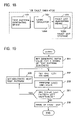
- FIG. 18 illustrates in block form an example of the construction of a fault simulator for use in an embodiment of the present invention.
- the fault simulator denoted generally by 100 , comprises: test pattern generating means 101 which generates test patterns one after another for input to a semiconductor IC under test; a logic simulator 102 which performs logic simulations of the operation of the IC under test by sequentially applying thereto the test patterns from the test pattern generating means 101 , then calculates logic signal value sequences occurring in signal lines of the IC under test, and stores them in a memory 102 M in correspondence with the respective test pattern sequences; and a fault list generating means 103 which generates list of faults detectable by a transient power supply current testing for each test pattern sequence through the use of the logic signal value sequence for each signal line calculated by the logic simulator 102 , and stores the fault list in a fault list storage 103 M.
- the test pattern generating means 101 , the logic simulator 102 and the fault list generating means 103 may be formed by either hardware or software.
- the test pattern generating means 101 is formed by three pseudo random pattern sequence generators, which are initialized to different values and driven in synchronization using the same clock to thereby generate random pattern sequences.
- the outputs from the three pseudo random pattern sequence generators are used as test patterns for each clock.
- a three-bit counter is used to count clocks, and for each clock the count value expressed by three bits is taken out as a test pattern. It will easily be understood that these schemes can be implemented by software. It is also possible to prestore required test patterns and read them out one after another.
- the number of shift stages of a pseudo random generator is selected or a sufficient number of test patterns is prestored in a memory so that various test patterns can be generated which provide sufficient data necessary for detecting, as detectable spots, delay faults in any logic gates or open faults in any signal lines in the semiconductor IC under test.
- logic simulator 102 With the logic simulator 102 by software, operations in respective logic gates of the semiconductor IC under test are sequentially conducted by software for each test pattern input thereto, and the operation results (logic signal values) for each test patterns are stored in correspondence with the signal lines where the operation results are provided. In this way, the logic signal value sequence in each signal line can easily be obtained.
- circuit information about the semiconductor IC is input to, for instance, a field programmable gate array (FPGA) to form a semiconductor IC under test, and upon input thereto of each test pattern, the logic signal value in each signal line is detected and stored in correspondence with the signal line.
- FPGA field programmable gate array
- the logic simulator 102 is provided with the memory 102 M for storing the logic signal values that are produced in respective signal lines for each test pattern.
- the logic simulator 102 may be such a general-purpose logic simulator as VHDL system simulator (VSS) by Synopsys. Inc.
- VHDL system simulator VHDL system simulator
- FIG. 19 depicts the procedure of the fault simulation method according to the present invention.
- the simulation starts from step 201 in which the test pattern generating means 101 sets the initial value for test patterns of a series of test pattern sequences for the fault list intended to make, that is, generates a test pattern of the initial value.
- the logic simulator 102 receives the test pattern set in step 201 .
- step 203 the logic simulator 102 uses the test pattern to perform a logic simulation of the operation of the semiconductor IC under test, then calculates logic signal values in signal lines in the IC under test, and stores in the memory 102 M the logic signal value for each signal line in correspondence with the test pattern.
- step 204 the fault simulator 100 makes a check to see if there is any test pattern left unattended in the test pattern sequence concerned. If so, the fault simulator 100 sets (generates) the next test pattern (for example, advances the operation of a pseudo random pattern generator by one clock), and repeats steps 202 and 203 . When there is not found any unattended test pattern left in the series of test pattern sequences (for example, when the pseudo random pattern generator has completed one round of random pattern generation) in step 204 , the fault simulator 100 goes to step 206 .
- the fault list generating means 103 generates a list of faults detectable by a transient-power supply current testing for the test pattern sequences, based on the logic signal value sequences produced in respective signal lines of the IC in the above steps and stored in the memory 102 M.
- the test pattern sequences are each composed of two test patterns as in the afore-mentioned example, two arbitrary test patterns generated by the test pattern generating means 102 are taken out and given a test pattern sequence identification number, and the signal lines in which logic signal values change in response to the application of the test patterns are associated, as fault-detectable spots, with the test pattern sequence identification number to make the list of faults.
- the generation of the fault list will be described in more detail later on.
- the time series of the logic signal values calculated by the logic simulator 102 for respective test patterns if steps 202 , 203 and 204 correspond to the time series of the test patterns in the test pattern sequence.
- FIG. 20 is a flowchart depicting an example of the procedure for generating the fault list in step 206 in FIG. 19 .
- the procedure begins with step 301 in which to select and initially set one of points that become possibly faulty in the semiconductor IC under test. This is followed by step 302 in which a check is made to determine whether the logic signal value sequence calculated by the logic simulator 102 satisfies the condition for fault detection by the transient power supply current testing when the above set point becomes faulty. If the fault detecting condition is met, the set point is registered in the fault list in step 303 . If it is found in step 302 that the fault detecting condition is not satisfied, the procedure proceeds to step 304 .
- step 304 a check is made to see if there is present in the IC under test any other unattended points that become possibly faulty; if so, the point that becomes possibly faulty next is set in step 305 , and then the procedure goes to step 302 . In this way, steps 302 , 303 , 304 and 305 are repeated until all of the points that become possibly faulty in the IC under test are dealt with; that is, no unattended points are found in step 304 , then the procedure ends.
- FIG. 21 is flowchart depicting an example of the procedure for generating a list of faults in logic gates in step 206 in FIG. 19 .
- the procedure begins with step 401 in which to select and initially set one of logic gates that become possibly faulty.
- step 402 a check is made to determine whether a change or changeover has been made in the logic signal value sequence in the output signal line of the set logic gate, calculated by the logic simulator 102 , based on the logic signal values in the output signal line of each logic gate stored for each test pattern sequence in the memory 102 M in which there are stored the results of the simulation in step 203 in FIG. 19 .
- the set logic gate and the corresponding test pattern are registered in the fault list in step 403 .
- the logic gate G 1 is set in the circuit of FIG. 14
- the logic signal value sequence in the output signal line (node) N 1 of the logic gate G 1 that is, the first logic signal value sequence “1, 1, 0, 0, . . . ” in third column of the FIG.
- test pattern sequences T 9 , T 10 , T 11 and T 12 that become R or F, and these test pattern sequences are registered for G 1 in the fault list, or G 1 is registered for each of those test pattern sequences T 9 to T 12 ; that is, these relationships are stored in the storage 103 M to make the fault list.
- faults detectable when the logic signal in the output signal line of the faulty logic gate takes a value R (a rising transition) and a value F (a falling transition), respectively, can also be registered as different faults.
- the fault detectable when the logic signal in its output signal line takes the value R and the fault detectable when the logic signal in its output signal line takes the value F are registered as G 1 R and G 1 F in the fault list, respectively.
- the logic signal in the output node N 1 of the logic gate G 1 takes the value F for any of the test patterns sequences T 9 , T 10 , T 11 and T 12 , these test pattern sequences are registered for the fault G 1 F in the fault list, or G 1 F is registered for each of those test patterns.
- step 402 If it is found in step 402 that the logic signal value sequence has not changed in the output signal line of the set logic gate, the procedure goes to step 404 .
- step 404 a check is made to determine whether there is still present an unattended logic gate in the semiconductor IC under test, and if such a logic gate is found, then the procedure goes to step 405 in which to set the logic gate where the next fault possibly occurs, followed by a return to step 402 . In this way, steps 402 , 403 , 404 and 405 are repeated until the logic gates in which faults possibly develop are all attended to or dealt with, and if no unattended logic gate is found in sep 404 , then the procedure ends.
- the transient power supply current of the semiconductor IC under test is measured at the time of inputting the test pattern sequence that causes the change in the logic signal value sequence. It can be decided whether the set logic gate is under the delay fault condition from the instantaneous value of the transient power supply current after a predetermined elapsed time, or the pulse width or integral of the transient power supply current as described previously. That is, in the generation of the fault list for each logic gate, to make a check to see if the logic signal value sequence has changed in the output signal line of the set logic gate is equivalent to making a check to determine whether the condition for fault detection by the transient power supply current testing is satisfied.
- FIG. 22 is a flowchart showing an example of the procedure for generating a list of faults in each signal line in step 206 in FIG. 19 .
- the procedure begins with step 501 in which to select and initially set one of signal lines in which a fault possibly develops.
- step 502 a check is made to determine whether a change has been made in the logic signal value sequence in the set signal line calculated by the logic simulator 102 in step 203 in FIG. 19 , based on the logic signal value sequence in the set signal line stored for each test pattern sequence in the memory 102 M wherein there are stored the results of the logic simulation performed in step 203 in FIG. 19 . If it is found that the logic signal value sequence has changed in the set signal line, then the procedure proceeds to step 503 .
- the logic signal value sequence in that signal line is the second sequence of logic signal values “0, 1, 0, 1, . . .” in the third column in the FIG. 17 table, and this logic signal value sequence is checked for R or F.
- R since R is found in the logic signal value sequence in association with the test pattern sequences T 5 , T 6 , T 7 and T 8 , that is, since the logic signal value sequence has been changed by these test pattern sequences, the procedure goes to step 503 . If no change is found in the logic signal value sequence in the set signal line, the procedure goes to step 505 .
- step 503 based on the results of calculations by the logic simulator 102 (the stored contents of the memory 102 M), a check is made to see if the logic signal value sequence in the output signal line of the logic gate with the set signal line connected to its input the has been changed by the test pattern sequence having caused that change in the logic signal value sequence in step 502 . If it is found that the logic signal value sequence has changed, the set signal line is registered in the fault list in step 504 . That is, in the above example, although the pattern sequences T 5 to T 8 change the logic signal value sequence in the set input signal line L 2 , it is the pattern sequences T 6 and T 8 , as indicated by F in the FIG.
- the test pattern sequences T 6 and T 8 are registered for the set signal line L 2 .
- the signal line L 2 is registered for T 6 and T 8 in the fault list. That is, the logic signal value sequence in the signal line L 2 is changed by the test pattern sequences T 5 to T 8 , but the logic gate G 2 responds only to the test pattern sequences T 6 and T 8 to perform switching, and since no fault cannot be detected by the transient power supply current testing without switching of the logic gate G 2 , the test pattern sequences T 6 and T 8 are registered for the signal line L 2 .
- step 503 If it is found in step 503 that the logic signal value sequence in the output signal line of the logic gate having connected to its input the set signal line has not been changed by the test pattern sequence found in step 502 to have changed the logic signal value sequence in the set input line, the procedure goes to step 505 .
- step 505 a check is made to see if there is any other signal lines left unchecked in the semiconductor IC under test, and if so, the signal line in which the next fault possibly occur is set in step 506 , followed by a return to step 502 . In this way, steps 502 , 503 , 504 , 505 and 506 are repeated until all the signal lines in which faults possibly occur are checked in the IC under test. If no signal line is found left unchecked in step 505 , the procedure ends.
- step 801 in which to select and initially set one of signal propagation paths in which a fault possibly develops.
- step 802 it is checked, for each test pattern sequence, whether the logic signal value sequence at every point of the set signal propagation path has changed, based on stored contents of the memory 102 M wherein there are stored the results of the logic simulation performed in step 203 in FIG. 19 .
- the logic signal sequence has changed at every point on the set signal propagation path, the corresponding test pattern sequence and the set signal propagation path are registered in the fault list in step 803 .
- the logic signal values at each input terminal, each internal node and each output terminal changes in response to the input of each test pattern sequence as shown in FIG. 15 .
- the FIG. 15 table shows that I 1 , N 1 , N 3 and O 1 are R, F, R and F, respectively, for the test pattern sequence T 9 ; that is, the logic signal values change at every point on this signal propagation path.
- I 1 , N 1 , N 3 and O 1 are R, F, R and F, respectively; that is, the logic signal values change at every point on this path. Accordingly, the test pattern sequences T 9 , T 10 and T 11 are registered for the signal propagation path ⁇ I 1 , N 1 , N 3 , O 1 >; alternatively, the path ⁇ I 1 , N 1 , N 3 , O 1 > is registered for each of the test pattern sequences T 9 , T 10 and T 11 .
- the logic signal values at each input terminal, each internal signal line and each output terminal change in response to the input of each test pattern sequence as depicted in the FIG. 17 table.
- the FIG. 17 table shows that I 3 , L 3 , L 5 , L 12 and O 2 are R, R, R, F and F, respectively for the test pattern sequence T 1 ; that is, the logic signal values change at every point on this signal propagation path.
- test pattern sequence T 2 too, I 3 , L 3 , L 5 , L 12 and O 2 are R, R, R, F and F, respectively; that is, the logic signal values change at every point on this path. Accordingly, the test pattern sequences T 1 and T 2 are registered in the fault list for the signal propagation path ⁇ I 3 , L 3 , L 5 , L 12 , O 2 >; alternatively, the path ⁇ I 3 , L 3 , L 5 , L 12 , O 2 > is registered for each of the test patterns T 1 and T 2 .
- the signal propagation paths that are registered in the fault list are not limited specifically to the paths from the input to the output terminal of the IC under test but may also be the signal propagation paths that do not reach the output terminal, such as ⁇ I 1 , N 1 > in the semiconductor IC of FIG. 14 and ⁇ I 1 , L 1 , L 6 > in the IC of FIG. 16 .
- step 802 In the case where it is found, in step 802 , that there is no test pattern sequence that causes the logic signal value sequence to change at every point on the path concerned or after the registration in the fault list in step 803 , it is checked in step 804 whether there still remains a signal propagation path left unchecked in the semiconductor IC under test. If an unchecked signal propagation path is found, the procedure goes to step 805 of setting a signal propagation path that become possibly faulty, followed by a return to step 803 . In this way, steps 802 , 803 , 804 and 805 are repeated as long as there remains such an unchecked signal propagation path that becomes possibly faulty. Upon completion of checking all the signal propagation paths that become possibly faulty, the fault list generating procedure ends.
- FIG. 24 is a table showing a fault list on the signal propagation paths obtained by logic simulations done as to whether the logic gates perform switching in the internal signal lines of the semiconductor IC of FIG. 14 .
- FIG. 25 is a table showing a fault list on the signal propagation paths obtained by logic simulations done as to whether the logic signal value sequences change in the internal signal lines of the semiconductor IC of FIG. 16 .
- the memories 102 M and 103 M may be formed by one memory.
- the fault list is generated after performing logic simulations using all the test pattern sequences
- An example of such a procedure is depicted in FIG. 26 .
- the semiconductor IC under test has three input terminals, three pseudo random pattern generators with different initial values are operated on the same clock to generate three random patterns, which are each input to a one-clock delay register.
- the test pattern sequences are each generated by taking out, as test patterns, the outputs from the three delay registers, then taking out, as test patterns, the outputs from the three random pattern generators, and combining the taken-out outputs.
- step 901 one of the test pattern sequences for which the fault list is desired to make is generated, for example, by combining the outputs from the delay registers and the pseudo random pattern generators as described above.
- step 902 one test pattern of the thus generated test pattern sequence is taken out in orderly sequence, and in step 903 a logic simulation of the operation of the semiconductor IC under test, using the taken-out test pattern, and logic signal values occurring in signal lines of the IC and stored in the memory 102 M for each signal line in correspondence with the test pattern used.
- step 904 it is checked whether there still remains in the test pattern sequence a test pattern left unused or unattended, and if so, the procedure goes to step 905 , in which the next test pattern is set (generated), for example, by setting the outputs from the pseudo random pattern generators, and then steps 902 and 903 are repeated.
- step 904 When no unattended test pattern is found in step 904 , the registration in the fault list takes place based on the results of the logic simulation using the test pattern sequence concerned. This process will be described later on. Then, the procedure goes to step 907 , in which it is checked whether there still remains a test pattern sequence left ungenerated, and if so, the procedure goes to step 901 , in which the next test pattern sequence is generated; for example, the operation of the pseudo random pattern generators is advanced by one clock. For the newly generated test pattern sequence, steps 902 to 906 are performed again. When no ungenerated test pattern sequence is found in step 907 , for example, when the pseudo random pattern generators have finished one round of generating the test pattern sequences, the procedure ends.
- step 401 one of logic gates that become possibly faulty in the semiconductor IC under test is initially set.
- step 402 it is checked from the stored contents 102 M whether the logic signal value sequence in the output signal line of the set logic gate, calculated by the logic simulator 102 for the test pattern sequence generated in step 901 in FIG. 26 , has been changed. If the logic signal value sequence has been changed in the output signal line of the set logic gate, the procedure goes to step 404 , in which the logic gate and the test pattern sequence concerned are registered in the fault list.
- the test pattern sequence generated in step 901 in FIG. 26 is T 9 in the FIG. 15 table.
- the logic gate G 1 in the circuit of FIG. 14 is set in step 401 in FIG. 21
- the logic signal value sequence in the output node N 1 of the logic gate G 1 is indicated by F in association with the test pattern sequence T 9 in the third column of the FIG. 15 table; that is, the logic signal value sequence is indicated to have been changed by the test pattern sequence T 9 .
- G 1 is registered for T 9 in the fault list; alternatively, T 9 is registered for G 1 .
- the fault that is detectable when the signal value in the output node of the faulty logic gate is R (a rising transition) and the fault that is detectable when the signal value in the output node is F (a falling transition) can also be registered as different faults.
- the logic gate G 1 when the logic gate G 1 is set, the two detectable faults mentioned above are registered as G 1 R and G 1 F in the fault list.
- T 9 since the signal value in the output node N 1 of the logic gate has the signal value F for the test pattern sequence T 9 , T 9 is registered for G 1 F in the fault list, or G 1 F is registered for the test pattern sequence T 9 . If the logic signal value sequence in the output node of the set logic gate has not changed, then the procedure goes to step 404 .
- step 404 a check is made to see if there still remains a logic gate left unchecked, and if so, the next logic gate that becomes possibly faulty is set in step 405 , followed by a return to step 402 . In this way, steps 402 , 403 , 404 and 405 are repeated until logic gates that become possibly faulty are all checked or attended to, and when no such an uncheckd or unattended logic gate is found, the procedure ends.
- processing is performed as to whether to register the test pattern sequence and the set logic gate in the fault list.
- step 501 one of the signal lines that become possibly faulty in the semiconductor IC under test is initialized.
- step 502 it is checked from the stored contents of the memory 102 M whether the logic signal sequence in the set signal line, calculated by the logic simulator for the test pattern sequence generated in step 901 in FIG. 26 , has been changed. If the logic signal value sequence has been changed in the set signal line, the procedure goes to step 503 , whereas when the logic signal value sequence has not been changed, the procedure goes to step 505 .
- step 503 it is checked whether the logic signal value sequence in the output signal line of the logic gate having its input connected to the set signal line, calculated by the logic simulator for the test pattern sequence generated in step 901 in FIG. 26 , has been changed. If the logic signal value sequence in the output signal line of the logic gate has been changed, the set signal line is registered in the fault list in step 504 , and the procedure goes to step 505 . For example, in the case where the test pattern T 1 in FIG. 17 is generated in step 901 in FIG. 26 and the signal line L 3 in the semiconductor IC of FIG. 16 is set in step 501 in FIG.
- step 505 a check is made to determine whether there is any other unchecked signal line that becomes possibly faulty. If such a signal line is found, the next signal line that becomes possibly faulty is set in step 506 , followed by a return to step 502 .
- steps 502 , 503 , 504 , 505 and 506 are repeated until all the signal lines that become possibly faulty in the semiconductor IC under test are checked. When no such an unchecked signal line is found, the procedure ends.
- the processing described above is performed upon each generation of the test pattern in step 901 .
- step 801 one or the signal propagation paths that become possibly faulty in the semiconductor IC under test is initially set.
- step 802 it is checked whether the logic signal value sequence at every point in the set signal propagation path, calculated by the logic simulator 102 for the test pattern sequence generated in step 901 in FIG. 26 , has been changed. If so, the procedure goes to step 803 , then the set signal propagation path is registered in the fault list, and the procedure goes to step 804 . For example, in the case where the test pattern T 9 in FIG. 15 is generated in step 901 in FIG.
- the logic signal value sequence changes at every point in the set signal propagation path, and consequently, the test pattern sequence T 9 is registered for the set signal propagation path ⁇ I 1 , N 1 , N 3 , O 1 > in the fault list, or ⁇ I 1 , N 1 , N 3 , O 1 > is registered for T 9 .
- the signal propagation paths that are registered in the fault list are not limited specifically to the paths from the input to the output terminal of the IC under test, but signal propagation paths that do not extend to the output terminal of the input terminal, such as ⁇ I 1 , N 1 > in the semiconductor IC of FIG. 14 and ⁇ I 1 , L 1 , L 6 > in FIG. 16 may also be registered. If no logic signal value sequence has been changed at any point in the set signal propagation path, the procedure goes to step 804 . In step 804 a check is made to see if there is still left unchecked a signal propagation path that become possibly faulty, and if so, the next signal propagation path that becomes possibly faulty is set in step 805 , followed by a return to step 802 .
- steps 802 , 803 , 804 and 805 are repeated until all the signal propagation paths that become possibly faulty in the semiconductor IC under test are checked. When no such an unchecked signal propagation path is found, the procedure ends.
- the processing described above is performed upon each generation of the test pattern in step 901 .
- FIG. 27 illustrates in block form another embodiment of the fault simulator according to the present invention.
- the fault simulator indicated generally by 600 , comprises test pattern sequence generating means 601 , fault inserting means 602 , a circuit simulator 603 and fault list generating means 604 .
- the test pattern sequence generating means 601 generates a test pattern sequence that is composed of two or more test patterns for input to the semiconductor IC under test.
- the fault inserting means 602 inserts an assumed fault into the semiconductor IC-under test.
- the circuit simulator 603 applies the test pattern sequence, generated by the test pattern sequence generating means, to the IC under test with the assumed fault inserted therein by the fault inserting means 602 and performs a circuit simulation, thereby calculating the transient power supply current of the IC under test.
- the fault list generating means 604 compares the transient power supply current, calculated by the circuit simulator 603 , with a transient power supply current of a normal circuit, then generates a fault list by deciding whether the fault is detectable by the transient power supply current using the test pattern sequence, and stores the fault list in the memory 604 M.
- the test pattern sequence generating means 601 , the fault inserting means 602 , the circuit simulator 603 and the fault list generating means can be formed by either hardware or software. There has been proposed a software configuration of the circuit simulator. According to the conventional scheme, connection information about the semiconductor IC for each transistor, for example, in the case of the circuit of FIG.
- connection information about how each transistor is connected is input to the circuit simulator, by which the semiconductor IC under test is constructed on software, then a model file of the characteristic of each transistor is read out according to set conditions and the transient power supply current responding to an input pattern is calculated by simulation.
- An open fault can be inserted by only inserting a high-resistance element in the point where the fault is assumed to lie, and a delay fault can be inserted by only inserting a delay element in the point where the fault is assumed to lie.
- the circuit simulator 603 may be a general-purpose circuit simulator, for example, Star-HSPICE by Avant! Corporation.
- FIG. 28 is a flowchart showing the procedure of another embodiment of the fault simulation method according to the present invention.
- the test pattern sequence generating means 601 generates in step 701 a test pattern sequence for which a fault list is desired to make.
- the fault inserting means 602 assumed one of faults that possibly occur in the semiconductor IC under test, and inserts the assumed fault into the IC.
- step 703 the circuit simulator 603 performs circuit simulations of the operation of the faulty circuit with the fault inserted therein in step 702 and a normal, fault-free circuit in the case of applying thereto the test pattern sequence generated in step 701 , and calculates the transient power supply currents of the both circuits.
- step 704 the fault list generating means 604 compares the transient power supply currents of the faulty and normal circuits calculated by the circuit simulator 603 , thereby making a check to determine where an abnormality developed in the transient power supply current of the faulty circuit. If an abnormality is found, then in step 705 the fault and the test pattern sequence corresponding thereto are registered in the fault list, that is, stored in the memory 604 M, and the procedure goes to step 706 . If no abnormality is found in step 704 , the procedure goes to step 706 . Finally, in step 706 it is checked whether there still remain in the IC under test possible fault left unattended.
- steps 702 , 703 , 704 and 705 are repeated until all the faults that possibly occur in the IC under test are dealt with.
- step 706 it is checked in step 707 whether any pattern sequences are left ungenerated. If so, the procedure returns to step 701 , and the same processing as mentioned above is performed again. If no ungenerated test pattern sequence is found, the procedure ends.
- the comparison of the transient power supply current of the faulty circuit with the transient power supply current of the normal circuit in step 704 may be made in their waveforms as well as in their instantaneous values, pulse widths or integrals after a predetermined elapsed time as referred to previously.
- the fault simulation method and the fault simulator according to the present invention are not limited specifically to the delay and open faults but are also applicable to a logic fault (a stack fault), short fault and a parameter abnormality fault of a MOS transistor by appropriately changing the fault detecting condition by the transient power supply current testing or a fault model. Further, the present invention is applicable to the cases where transient power supply currents of not only MOS transistor ICs but also all kinds of semiconductor ICs become abnormal due to faults. While in the above the test pattern sequence has been described to be composed of two test patterns, three or more test patterns can also be used.
- the fault simulation method it is possible, with the use of the transient power supply current testing scheme of high observability and having switching information about logic gates, to generate a list of faults detectable by the transient power supply current testing for the delay fault or open fault leading to the delay fault for which no fault list could have been generated in the past.
- the method according to the present invention significantly improves the efficiency of testing the delay fault and open faults.
Abstract
Description
I Gf =I Sf +I C. (1)
IGr=ISr (2)
where ISmax is the maximum value of the transient current (short circuit current) IS flowing into the CMOS inverter, VDD is the power supply voltage at the power supply terminal TVD, VTHN is a threshold voltage of the n-MOS transistor, VTHP is a threshold voltage of the p-MOS transistor and tr is the rising transition time of the input voltage VIN. Note that the threshold voltage VTHP is shown in absolute value. Further, to simplify the approximate expression, the input voltage VIN is shown to start the transition at
where tf is the falling transition time of the input voltage VIN. For precaution's sake, the rise start time of the power supply current, the time of its maximum value ISmax and its fall end time are shown in parentheses in
where N is the number of logic gates that are switched by an input test pattern sequence; N=4 in the example of
t gdi=τi−τi-1 (7)
Accordingly, the path delay time tpd of the path P can be calculated, as the sum of gate delay times tgdi, by
However, the actual gate delay time tgdi varies under the influence of a fault.
t gdi =t gdi,typ+δi,1≦i≦m (9)
where tgdj,typ is a typical value of the delay time of the logic gate G1 and δi is a variation component of the gate delay time. For example, an open fault increases the delay time of a faulty logic gate alone but does not increase the delay time of a fault-free or normal logic gate. And a parameter abnormality fault increases the delay time of every logic gate. With a change in the gate delay time, the path delay time tpd also undergoes a similar change, which can be expressed by the following equation.
where tpd,typ is a typical value of the delay time of the path P and Δ is a variation component of the path delay time.
t pd +T SU <T CLK −T SKW (11)
where TSU is a signal set-up time, TCKL is the period of the system clock CLK and TSKW is a clock skew of the system clock CKL (the amount of ± variations of the edge of the clock CLK due to its jitter). Modifying Eq. (11) gives
t pd <T CLK −T SKW −T SU ≡T′ (12)
That is, the delay time tpd of the path P needs to be shorter than the time (T′) obtained by subtracting from the clock period TCLK such margins as the set-up time TSU and the clock skew TSKW. If tpd is larger than T′, then the signal propagation over the path P lags behind the system clock at which to latch it in the output latch; so that the circuit does not operate normally. This state is defined as the delay fault. That is, it is defined that the path P has a delay fault when the delay time tpd is longer than the predetermined time T′, where T′ is the permissible upper limit value of the delay time.
Open Fault (Accompanied by Delay Fault)
Accordingly, The maximum value tpd,max of the path delay time in the paths P1, . . . , Pn can be calculated as the time interval between the time τmax and the input transition time τ0 by
t pd,max=τmax−τ0 (14)
t PW≡τIDD−τ0 (15)
t PW=τIDD−τ0≦τmax−τ0 =t pd,max (16)
If the pulse width tPW is larger than the permissible upper limit value T′ of the delay time,
T′<tPW≦tpd,max (17)
In the path of the largest delay time tpd,max, the signal propagation lags behind the system clock. That is, the delay fault is present in the circuit. Hence, tPW larger than T′ indicates the presence of the delay fault in any one of the activated paths, whereas tPW smaller than T′ indicates the absence of the delay fault in any of the activated paths.
Delay fault absent: tPW≦T′
Delay fault present: tPW>T′ (18)
I′≡DDT(τmax) (19)
The following equation holds at the time t where t≧τmax:
i DDT(t)≦i DDT(τmax)=I′, t≧τ max (20)
For normal circuit operation, the maximum path delay time tpd,max needs to be smaller than the upper limit value T′ (=TCLK−TSKW−TSU) of the delay time.
T pd,max=τmax−τ0 <T′ (21)
Accordingly, when the circuit is fault-free, the following equation holds from Eq. (20) at the time t where t=T′+τ0>τmax.
i DDT(T′+τ 0)≦I′ (22)
If the instantaneous value of the transient power supply current waveform iDDT at the time T′+τ0 is larger than the value I′, that is, if
i DDT(T′+τ 0)>I′=i DDT(τmax) (23)
it follows that
τmax >T′+τ 0 (24)
∴t pd,max=τmax−τ0 >T′ (25)
because T′+τ0 cannot be larger than τmax. In the path of the largest delay time tpd,max, the signal propagation lags behind the system clock. That is, the delay fault is present in the circuit. Accordingly, that the power supply current value iDDT(T′+τ0) at the time T′+τ0 is larger than I′ indicates the presence of the delay fault in any one of the activated paths. Conversely, the power supply current value iDDT(T′+τ0) smaller than I′ indicates the absence of the delay fault in any of the activated paths.
Delay Fault Present: iDDT(T′+τ 0)≦I′
Delay Fault Absent: iDDT(T′+τ 0)>I′ (26)
This relationship is shown in
Accordingly, the integral QS of the short circuit current flowing through the logic gate at the time of switching is given by
where tr is the input signal transition time. That is, the integral QS of the short circuit current IS (ISr or ISf) flowing into the logic gate is in proportion to the input transition time tr of the logic gate. Further, it will be seen that the integral QS is irrespective of whether the direction of the input signal transition is a rising or falling transition.
The integral QC is not dependent on the input transition time tr of the CMOS inverter.
That is, the integral of the transient current of the logic gate is in proportion to its input transition time.
In the example of
where an is a proportional coefficient between the integral QSn of the short circuit current of the logic gate Gn and its input transition time trn, and b is a constant term that is expressed as the sum of charging currents QCn flowing into the respective logic gates.
Open Fault
t r ≈t T,typ+2.2R open C in (35)
where tT,typ is a typical value of the transition time of the input signal when no fault is present. The transition time tT was calculated as the time necessary for the voltage value to rise from 0.1 VDD up to 0.9 VDD (or for the voltage value to fall from 0.9 VDD down to 0.1 VDD). 2.2RopenCin is the time needed for the parasitic capacitance (Cin) to rise from 0.1 VDD UP to 0.9 VDD; this value was calculated by loge(0.9 VDD/0.1 VDD)×RopenCin. That is, the increment of the input signal transition time of the inverter is in proportion to the resistance value Ropen of the open fault. Accordingly, when an open fault is present in the input of a k-th inverter on the path under test, the integral QDDT of the power supply current of the CMOS IC is given by the following equation (36) from Eqs. (34) and (35), and it varies linearly with the resistance value Ropen of the open fault, and the increment is in proportion to the resistance value Ropen.
where QDDT,typ is a typical value of the integral of the power supply current in the case of no fault. 2.2akCinRopen in the second term on the right-hand side of Eq. (36) is the amount of addition based on the open fault in the input of the k-th inverter. Eq. (36) also agrees with the results of simulation about variations in the integral QDDT with the resistance value Ropen shown in
Open Fault Absent: QDDT≦QDDT,typ+ΔQ
Open Fault Present: QDDT>QDDT,typ+ΔQ (37)
QDDT,typ and ΔQ can be derived, for example, by a simulation about process variations.
Method for Detecting Delay Fault by Fault in Input Stage (Using the Integral of the Transient Power Supply Current)
where tgd,step is the delay time of a fault-free inverter for a step input with no transition time. Further, VTH is a threshold voltage of a p-MOS or n-MOS, which is given by VTH=VTHN for a rising transition of the input and by VTH=VTHP for a falling transition of the input. Since the input transition time of the logic gate is given by Eq. (35), the delay time tgd of a logic gate having an open fault in the input signal line that can be modeled by the resistance Ropen can be calculated by substituting Eq. (35) into Eq. (38).
In the above, tgd,typ is a typical value of the delay time of a fault-free logic gate. That is, the delay time of a logic gate with the open fault varies with the resistance value Ropen of the fault, and the increment δ of the gate delay time is in proportion to the resistance value Ropen. Therefore, when an open fault is present in the input of any one of the logic gates on the path under test, the delay time tpd of the path under test is also in proportion to the resistance value Ropen. This can be understood from the fact that substituting Eq. (39) into Eq. (10) gives the following equation (40).
This also agrees with the results of a simulation for variations in the path delay time tpd with respect to the resistance value Ropen shown in
Therefore, the integral QDDT of the transient power supply current of the IC is calculated from Eq. (34) as follows:
and the integral QDDT of the transient power supply current of the circuit is also in proportion to the resistance value Ropen of the open fault.
Letting Qmax represent the integral of the transient power supply current at the time when the path delay time tpd reaches the permissible upper limit value T′ of the delay time, the following equation (43) is obtained by calculating Qmax with tpd=T′ and QDDT=Qmax in Eq. (42).
The value Qmax is the upper limit value of the integral QDDT of the transient power supply current of a CMOS IC with no delay fault. That is, the value QDDT smaller than the upper limit value Qmax, indicates the absence of the delay fault in the CMOS IC, and the value QDDT larger than the value Qmax indicates the presence of the delay fault.
Delay Fault Absent: QDDT≦Qmax
Delay Fault Present: QDDT>Qmax (44)
Claims (9)
Applications Claiming Priority (1)
| Application Number | Priority Date | Filing Date | Title |
|---|---|---|---|
| JP2000014962A JP2001208803A (en) | 2000-01-24 | 2000-01-24 | Simulation method for failure of semiconductor integrated circuit, and failure simulator |
Publications (1)
| Publication Number | Publication Date |
|---|---|
| US6975978B1 true US6975978B1 (en) | 2005-12-13 |
Family
ID=18542334
Family Applications (1)
| Application Number | Title | Priority Date | Filing Date |
|---|---|---|---|
| US09/699,077 Expired - Fee Related US6975978B1 (en) | 2000-01-24 | 2000-10-27 | Method and apparatus for fault simulation of semiconductor integrated circuit |
Country Status (3)
| Country | Link |
|---|---|
| US (1) | US6975978B1 (en) |
| JP (1) | JP2001208803A (en) |
| DE (1) | DE10053758A1 (en) |
Cited By (30)
| Publication number | Priority date | Publication date | Assignee | Title |
|---|---|---|---|---|
| US20040078183A1 (en) * | 2002-10-21 | 2004-04-22 | Victor Drabkin | System and method of system response testing and modeling |
| US20040117169A1 (en) * | 2002-12-17 | 2004-06-17 | International Business Machines Corporation | Method and system for short-circuit current modeling in CMOS integrated circuits |
| US20050155005A1 (en) * | 2003-03-06 | 2005-07-14 | Fujitsu Limited | Circuit analyzing device, circuit analyzing method, program, and computer readable information recording medium |
| US20060031731A1 (en) * | 2000-06-08 | 2006-02-09 | Advantest Corporation | Generating test patterns used in testing semiconductor integrated circuit |
| US20060053357A1 (en) * | 2004-09-06 | 2006-03-09 | Janusz Rajski | Integrated circuit yield and quality analysis methods and systems |
| US20060265681A1 (en) * | 2005-05-19 | 2006-11-23 | International Business Machines Corporation | An automated and electrically robust method for placing power gating switches in voltage islands |
| US20060277511A1 (en) * | 2005-06-01 | 2006-12-07 | Bhavna Agrawal | System and method for memory element characterization |
| US20070001686A1 (en) * | 2005-06-29 | 2007-01-04 | Parker Kenneth P | Methods and apparatus for non-contact testing and diagnosing of open connections on non-probed nodes |
| US20070001687A1 (en) * | 2005-06-29 | 2007-01-04 | Schneider Myron J | Method for using internal semiconductor junctions to aid in non-contact testing |
| US20070080706A1 (en) * | 2005-10-11 | 2007-04-12 | Mitsubishi Denki Kabushiki Kaisha | Logic circuit for board power-supply evaluation and board power-supply evaluating method |
| US7295031B1 (en) * | 2006-07-12 | 2007-11-13 | Agilent Technologies, Inc. | Method for non-contact testing of marginal integrated circuit connections |
| US20070277062A1 (en) * | 2005-02-11 | 2007-11-29 | Hyatt Steven J | Connection error avoidance for apparatus connected to a power supply |
| US20070296443A1 (en) * | 2006-06-13 | 2007-12-27 | Heaberlin Douglas C | Exhaustive diagnosis of bridging defects in an integrated circuit |
| US20080126293A1 (en) * | 2006-09-21 | 2008-05-29 | International Business Machines Corporation | Method and apparatus for dynamically creating scenario based test designs from hierarchical use cases |
| US20080263400A1 (en) * | 2007-04-23 | 2008-10-23 | Microsoft Corporation | Fault insertion system |
| US20080263481A1 (en) * | 2004-05-19 | 2008-10-23 | Altera Corporation | Apparatus and methods for power management in integrated circuits |
| US20090254331A1 (en) * | 2008-04-02 | 2009-10-08 | Synopsys, Inc. | Compact circuit-simulation output |
| US20100058131A1 (en) * | 2008-08-29 | 2010-03-04 | Advantest Corporation | Test apparatus, test vector generate unit, test method, program, and recording medium |
| US20100095179A1 (en) * | 2007-04-23 | 2010-04-15 | Kyushu Institute Of Technology | Test pattern generation method for avoiding false testing in two-pattern testing for semiconductor integrated circuit |
| US20100107134A1 (en) * | 2008-10-29 | 2010-04-29 | Nec Electronics Corporation | Designing apparatus, designing method, and designing program for semiconductor integrated circuit |
| US20100114520A1 (en) * | 2008-10-30 | 2010-05-06 | Advantest Corporation | Test apparatus, test method, program, and recording medium reducing the influence of variations |
| US20100238700A1 (en) * | 2009-03-17 | 2010-09-23 | Seagate Technology Llc | Quiescent Testing of Non-Volatile Memory Array |
| US20130110487A1 (en) * | 2011-10-27 | 2013-05-02 | International Business Machines Corporation | Detection of unchecked signals in circuit design verification |
| US8776006B1 (en) * | 2013-02-27 | 2014-07-08 | International Business Machines Corporation | Delay defect testing of power drop effects in integrated circuits |
| CN105606300A (en) * | 2015-12-21 | 2016-05-25 | 合肥工业大学 | Battery-powered multi-dimensional force strain sensor fault diagnosis system |
| CN106596035A (en) * | 2016-12-07 | 2017-04-26 | 中国航天空气动力技术研究院 | Device used for wind tunnel strain type balance state-of-health monitoring |
| US10466070B2 (en) * | 2015-08-28 | 2019-11-05 | Denso Corporation | Disconnection detector |
| US10969428B2 (en) * | 2015-12-31 | 2021-04-06 | Samsung Electronics Co., Ltd. | Method of inspecting pattern defect |
| US10969429B1 (en) * | 2019-08-13 | 2021-04-06 | Cadence Design Systems, Inc. | System and method for debugging in concurrent fault simulation |
| US11042679B1 (en) * | 2020-08-31 | 2021-06-22 | Siemens Industry Software Inc. | Diagnosis resolution prediction |
Families Citing this family (3)
| Publication number | Priority date | Publication date | Assignee | Title |
|---|---|---|---|---|
| CN106646174B (en) * | 2016-09-30 | 2018-03-16 | 浙江大学 | A kind of high speed three-dimensional electrology characteristic test system applied to transistor |
| CN110597694A (en) * | 2019-08-09 | 2019-12-20 | 深圳木成林科技有限公司 | Method and terminal for monitoring front-end page |
| CN116594830B (en) * | 2023-03-17 | 2024-03-01 | 芯华章科技(北京)有限公司 | Hardware simulation tool, debugging method and storage medium |
Citations (16)
| Publication number | Priority date | Publication date | Assignee | Title |
|---|---|---|---|---|
| US5483170A (en) * | 1993-08-24 | 1996-01-09 | New Mexico State University Technology Transfer Corp. | Integrated circuit fault testing implementing voltage supply rail pulsing and corresponding instantaneous current response analysis |
| US5552744A (en) * | 1994-08-11 | 1996-09-03 | Ltx Corporation | High speed IDDQ monitor circuit |
| US5726997A (en) * | 1993-10-12 | 1998-03-10 | At & T Global Inf Solution | Apparatus and method for testing of integrated circuits |
| EP0878761A1 (en) | 1997-05-13 | 1998-11-18 | Nec Corporation | Method and apparatus for diagnosing failure occurrence position |
| US5850404A (en) * | 1995-01-20 | 1998-12-15 | Nec Corporation | Fault block detecting system using abnormal current |
| US5949798A (en) * | 1996-02-06 | 1999-09-07 | Nec Corporation | Integrated circuit fault testing system based on power spectrum analysis of power supply current |
| US5953519A (en) * | 1995-06-12 | 1999-09-14 | Fura; David A. | Method and system for generating electronic hardware simulation models |
| US6031386A (en) * | 1997-10-31 | 2000-02-29 | Sandia Corporation | Apparatus and method for defect testing of integrated circuits |
| US6140832A (en) * | 1998-06-05 | 2000-10-31 | Raytheon Company | Method of utilizing IDDQ tests to screen out defective parts |
| US6163763A (en) * | 1998-10-06 | 2000-12-19 | Cadence Design Systems, Inc. | Method and apparatus for recording and viewing error data generated from a computer simulation of an integrated circuit |
| US6175244B1 (en) * | 1997-04-25 | 2001-01-16 | Carnegie Mellon University | Current signatures for IDDQ testing |
| US6182258B1 (en) * | 1997-06-03 | 2001-01-30 | Verisity Ltd. | Method and apparatus for test generation during circuit design |
| US6461882B2 (en) * | 2000-06-19 | 2002-10-08 | Advantest Corporation | Fault simulation method and fault simulator for semiconductor integrated circuit |
| US6513137B1 (en) * | 1999-10-18 | 2003-01-28 | Cardiac Pacemakers, Inc. | Test method and apparatus using energy consumption ratio |
| US6593765B1 (en) * | 1999-09-17 | 2003-07-15 | Advantest, Corp. | Testing apparatus and testing method for semiconductor integrated circuit |
| US6801049B2 (en) * | 2000-04-04 | 2004-10-05 | Advantest Corporation | Method and apparatus for defect analysis of semiconductor integrated circuit |
Family Cites Families (1)
| Publication number | Priority date | Publication date | Assignee | Title |
|---|---|---|---|---|
| US5321354A (en) * | 1990-07-23 | 1994-06-14 | Seiko Epson Corporation | Method for inspecting semiconductor devices |
-
2000
- 2000-01-24 JP JP2000014962A patent/JP2001208803A/en active Pending
- 2000-10-27 US US09/699,077 patent/US6975978B1/en not_active Expired - Fee Related
- 2000-10-30 DE DE10053758A patent/DE10053758A1/en not_active Ceased
Patent Citations (18)
| Publication number | Priority date | Publication date | Assignee | Title |
|---|---|---|---|---|
| US5483170A (en) * | 1993-08-24 | 1996-01-09 | New Mexico State University Technology Transfer Corp. | Integrated circuit fault testing implementing voltage supply rail pulsing and corresponding instantaneous current response analysis |
| US5726997A (en) * | 1993-10-12 | 1998-03-10 | At & T Global Inf Solution | Apparatus and method for testing of integrated circuits |
| US5552744A (en) * | 1994-08-11 | 1996-09-03 | Ltx Corporation | High speed IDDQ monitor circuit |
| US5850404A (en) * | 1995-01-20 | 1998-12-15 | Nec Corporation | Fault block detecting system using abnormal current |
| US5953519A (en) * | 1995-06-12 | 1999-09-14 | Fura; David A. | Method and system for generating electronic hardware simulation models |
| US5949798A (en) * | 1996-02-06 | 1999-09-07 | Nec Corporation | Integrated circuit fault testing system based on power spectrum analysis of power supply current |
| US6175244B1 (en) * | 1997-04-25 | 2001-01-16 | Carnegie Mellon University | Current signatures for IDDQ testing |
| EP0878761A1 (en) | 1997-05-13 | 1998-11-18 | Nec Corporation | Method and apparatus for diagnosing failure occurrence position |
| US6347388B1 (en) * | 1997-06-03 | 2002-02-12 | Verisity Ltd. | Method and apparatus for test generation during circuit design |
| US6182258B1 (en) * | 1997-06-03 | 2001-01-30 | Verisity Ltd. | Method and apparatus for test generation during circuit design |
| US6031386A (en) * | 1997-10-31 | 2000-02-29 | Sandia Corporation | Apparatus and method for defect testing of integrated circuits |
| US6140832A (en) * | 1998-06-05 | 2000-10-31 | Raytheon Company | Method of utilizing IDDQ tests to screen out defective parts |
| US6163763A (en) * | 1998-10-06 | 2000-12-19 | Cadence Design Systems, Inc. | Method and apparatus for recording and viewing error data generated from a computer simulation of an integrated circuit |
| US6593765B1 (en) * | 1999-09-17 | 2003-07-15 | Advantest, Corp. | Testing apparatus and testing method for semiconductor integrated circuit |
| US6513137B1 (en) * | 1999-10-18 | 2003-01-28 | Cardiac Pacemakers, Inc. | Test method and apparatus using energy consumption ratio |
| US6801049B2 (en) * | 2000-04-04 | 2004-10-05 | Advantest Corporation | Method and apparatus for defect analysis of semiconductor integrated circuit |
| US6828815B2 (en) * | 2000-04-04 | 2004-12-07 | Advantest Corporation | Method and apparatus for defect analysis of semiconductor integrated circuit |
| US6461882B2 (en) * | 2000-06-19 | 2002-10-08 | Advantest Corporation | Fault simulation method and fault simulator for semiconductor integrated circuit |
Non-Patent Citations (13)
| Title |
|---|
| Acuna, E.L. et al. "Simulation Techniques for Mixed Analog / Digital Circuits." IEEE Journal of Solid-State Circuits. vol. 25, Issue 2. pp. 353-363. * |
| Agrawal, V. "Contest: A Concurrent Test Generator for Sequential Circuits." Proc. 25th ACM/IEEE DAC, 1988. 1988. pp. 84-89. * |
| Beasley et al. "Idd Pulse Response Testing : A Unified Approach to Testing Digital and Analogue ICs." Electronics Letters. Nov. 25, 1993. pp. 2101-2103. * |
| Beasley et al. "Idd Pulse Response Testing on Analog and Digital CMOS Circuits." Proc. Int'l Test Conf, 1993. Oct. 21, 1993. pp. 626-634. * |
| Carmichael, N. et al. "Simulation as an Aid to Power Supply Diagnostics". AUTOTESTCON '95. Aug. 8-10, 1995. pp. 556-560. * |
| Jian Liu, et al. "Dynamic Power Supply Current Testing of CMOS SRAMs." Proc. 7th Asian Test Symposium, 1998. Dec. 4, 1998. pp. 348-353. * |
| Jian Liu, et al. "Power Supply Current Detectability of SRAM Defects." Proc. Of 4th Asian Test Symposium. Nov. 24, 1995. pp. 367-373. * |
| Jiang, W. and Vinnakota, B. "IC Test Using the Energy Consumption Ratio." Proc. 36th ACM/IEEE DAC. 1999. pp. 976-981. * |
| Makki, R. et al. "Transient Power Supply Current Testing of Digital CMOS Circuits." Proc. Int'l Test Conf, 1995. Oct. 25, 1996. pp. 892-901. * |
| Plusquellic, J.F. et al. "Digital IC Device Testing by Transient Signal Analysis (TSA)." Electronics Letters. Aug. 31, 1995. pp. 1568-1570. * |
| Plusquellic, J.F. et al. "Digital Integrated Circuit Testing Using Transient Signal Analysis." Proc. Int'l Test Conf, 1996. Oct. 25, 1996. pp. 481-490. * |
| Segura, J.A. "An Approach to Dynamic Power Consumption Current Testing of CMOS ICs." Proc. 13th IEEE VLSI Test Symposium, 1995. May 3, 1995. pp. 95-100. * |
| Shyang-Tai, Su et al. "Dynamic Power Supply Current Monitoring of SRAMs." Proc. 7th Annual IEEE Int'l ASIC Conf. and Exhibit, 1994. Sep. 23, 1994. pp. 370-373. * |
Cited By (63)
| Publication number | Priority date | Publication date | Assignee | Title |
|---|---|---|---|---|
| US20060031731A1 (en) * | 2000-06-08 | 2006-02-09 | Advantest Corporation | Generating test patterns used in testing semiconductor integrated circuit |
| US20060041810A1 (en) * | 2000-06-08 | 2006-02-23 | Advantest Corporation | Generating test patterns used in testing semiconductor integrated circuit |
| US7254764B2 (en) * | 2000-06-08 | 2007-08-07 | Advantest Corporation | Generating test patterns used in testing semiconductor integrated circuit |
| US7225377B2 (en) * | 2000-06-08 | 2007-05-29 | Advantest Corporation | Generating test patterns used in testing semiconductor integrated circuit |
| US20040078183A1 (en) * | 2002-10-21 | 2004-04-22 | Victor Drabkin | System and method of system response testing and modeling |
| US7191113B2 (en) * | 2002-12-17 | 2007-03-13 | International Business Machines Corporation | Method and system for short-circuit current modeling in CMOS integrated circuits |
| US20040117169A1 (en) * | 2002-12-17 | 2004-06-17 | International Business Machines Corporation | Method and system for short-circuit current modeling in CMOS integrated circuits |
| US20050155005A1 (en) * | 2003-03-06 | 2005-07-14 | Fujitsu Limited | Circuit analyzing device, circuit analyzing method, program, and computer readable information recording medium |
| US7739638B2 (en) * | 2003-03-06 | 2010-06-15 | Fujitsu Limited | Circuit analyzing device, circuit analyzing method, program, and computer readable information recording medium considering influence of signal input to peripheral circuit which does not have logical influence |
| US20080263481A1 (en) * | 2004-05-19 | 2008-10-23 | Altera Corporation | Apparatus and methods for power management in integrated circuits |
| US20140258956A1 (en) * | 2004-05-19 | 2014-09-11 | Altera Corporation | Apparatus and methods for power management in integrated circuits |
| US8732635B2 (en) * | 2004-05-19 | 2014-05-20 | Altera Corporation | Apparatus and methods for power management in integrated circuits |
| US20090210183A1 (en) * | 2004-09-06 | 2009-08-20 | Janusz Rajski | Determining and analyzing integrated circuit yield and quality |
| US7512508B2 (en) | 2004-09-06 | 2009-03-31 | Janusz Rajski | Determining and analyzing integrated circuit yield and quality |
| US7987442B2 (en) | 2004-09-06 | 2011-07-26 | Mentor Graphics Corporation | Fault dictionaries for integrated circuit yield and quality analysis methods and systems |
| US20060066338A1 (en) * | 2004-09-06 | 2006-03-30 | Janusz Rajski | Fault dictionaries for integrated circuit yield and quality analysis methods and systems |
| US20060066339A1 (en) * | 2004-09-06 | 2006-03-30 | Janusz Rajski | Determining and analyzing integrated circuit yield and quality |
| US20060053357A1 (en) * | 2004-09-06 | 2006-03-09 | Janusz Rajski | Integrated circuit yield and quality analysis methods and systems |
| US8253275B2 (en) | 2005-02-11 | 2012-08-28 | International Business Machines Corporation | Connection error avoidance for apparatus connected to a power supply |
| US20100204935A1 (en) * | 2005-02-11 | 2010-08-12 | International Business Machines Corporation | Connection error avoidance for apparatus connected to a power supply |
| US7759820B2 (en) * | 2005-02-11 | 2010-07-20 | International Business Machines Corporation | Connection error avoidance for apparatus connected to a power supply |
| US20070277062A1 (en) * | 2005-02-11 | 2007-11-29 | Hyatt Steven J | Connection error avoidance for apparatus connected to a power supply |
| US7266797B2 (en) * | 2005-05-19 | 2007-09-04 | International Business Machines Corporation | Automated and electrically robust method for placing power gating switches in voltage islands |
| US20060265681A1 (en) * | 2005-05-19 | 2006-11-23 | International Business Machines Corporation | An automated and electrically robust method for placing power gating switches in voltage islands |
| US20080155484A1 (en) * | 2005-06-01 | 2008-06-26 | Bhavna Agrawal | System and method for memory element characterization |
| US7350170B2 (en) * | 2005-06-01 | 2008-03-25 | International Business Machines Corporation | System and method for memory element characterization |
| US20060277511A1 (en) * | 2005-06-01 | 2006-12-07 | Bhavna Agrawal | System and method for memory element characterization |
| US7242198B2 (en) * | 2005-06-29 | 2007-07-10 | Agilent Technologies, Inc. | Method for using internal semiconductor junctions to aid in non-contact testing |
| US20070001686A1 (en) * | 2005-06-29 | 2007-01-04 | Parker Kenneth P | Methods and apparatus for non-contact testing and diagnosing of open connections on non-probed nodes |
| US7362106B2 (en) * | 2005-06-29 | 2008-04-22 | Agilent Technologies, Inc. | Methods and apparatus for non-contact testing and diagnosing of open connections on non-probed nodes |
| US7327148B2 (en) * | 2005-06-29 | 2008-02-05 | Agilent Technologies, Inc. | Method for using internal semiconductor junctions to aid in non-contact testing |
| US20070001687A1 (en) * | 2005-06-29 | 2007-01-04 | Schneider Myron J | Method for using internal semiconductor junctions to aid in non-contact testing |
| US20070001688A1 (en) * | 2005-06-29 | 2007-01-04 | Schnelder Myron J | Method for using internal semiconductor junctions to aid in non-contact testing |
| US7301361B2 (en) * | 2005-10-11 | 2007-11-27 | Mitsubishi Denki Kabushiki Kaisha | Logic circuit for board power-supply evaluation and board power-supply evaluating method |
| US20070080706A1 (en) * | 2005-10-11 | 2007-04-12 | Mitsubishi Denki Kabushiki Kaisha | Logic circuit for board power-supply evaluation and board power-supply evaluating method |
| US7352170B2 (en) | 2006-06-13 | 2008-04-01 | International Business Machines Corporation | Exhaustive diagnosis of bridging defects in an integrated circuit including multiple nodes using test vectors and IDDQ measurements |
| US20070296443A1 (en) * | 2006-06-13 | 2007-12-27 | Heaberlin Douglas C | Exhaustive diagnosis of bridging defects in an integrated circuit |
| US7295031B1 (en) * | 2006-07-12 | 2007-11-13 | Agilent Technologies, Inc. | Method for non-contact testing of marginal integrated circuit connections |
| US20080126293A1 (en) * | 2006-09-21 | 2008-05-29 | International Business Machines Corporation | Method and apparatus for dynamically creating scenario based test designs from hierarchical use cases |
| US8001437B2 (en) * | 2007-04-23 | 2011-08-16 | Kyushu Institute Of Technology | Test pattern generation method for avoiding false testing in two-pattern testing for semiconductor integrated circuit |
| US20080263400A1 (en) * | 2007-04-23 | 2008-10-23 | Microsoft Corporation | Fault insertion system |
| US20100095179A1 (en) * | 2007-04-23 | 2010-04-15 | Kyushu Institute Of Technology | Test pattern generation method for avoiding false testing in two-pattern testing for semiconductor integrated circuit |
| US8706467B2 (en) * | 2008-04-02 | 2014-04-22 | Synopsys, Inc. | Compact circuit-simulation output |
| US20090254331A1 (en) * | 2008-04-02 | 2009-10-08 | Synopsys, Inc. | Compact circuit-simulation output |
| US7984353B2 (en) * | 2008-08-29 | 2011-07-19 | Advantest Corporation | Test apparatus, test vector generate unit, test method, program, and recording medium |
| US20100058131A1 (en) * | 2008-08-29 | 2010-03-04 | Advantest Corporation | Test apparatus, test vector generate unit, test method, program, and recording medium |
| US20100107134A1 (en) * | 2008-10-29 | 2010-04-29 | Nec Electronics Corporation | Designing apparatus, designing method, and designing program for semiconductor integrated circuit |
| US8250511B2 (en) * | 2008-10-29 | 2012-08-21 | Renesas Electronics Corporation | Designing apparatus, designing method, and designing program for semiconductor integrated circuit |
| US8185336B2 (en) * | 2008-10-30 | 2012-05-22 | Advantest Corporation | Test apparatus, test method, program, and recording medium reducing the influence of variations |
| TWI392887B (en) * | 2008-10-30 | 2013-04-11 | Advantest Corp | Test apparatus, test method and recording medium |
| US20100114520A1 (en) * | 2008-10-30 | 2010-05-06 | Advantest Corporation | Test apparatus, test method, program, and recording medium reducing the influence of variations |
| US8526252B2 (en) * | 2009-03-17 | 2013-09-03 | Seagate Technology Llc | Quiescent testing of non-volatile memory array |
| US20100238700A1 (en) * | 2009-03-17 | 2010-09-23 | Seagate Technology Llc | Quiescent Testing of Non-Volatile Memory Array |
| US20130110487A1 (en) * | 2011-10-27 | 2013-05-02 | International Business Machines Corporation | Detection of unchecked signals in circuit design verification |
| US9057764B2 (en) * | 2011-10-27 | 2015-06-16 | International Business Machines Corporation | Detection of unchecked signals in circuit design verification |
| US8776006B1 (en) * | 2013-02-27 | 2014-07-08 | International Business Machines Corporation | Delay defect testing of power drop effects in integrated circuits |
| US10466070B2 (en) * | 2015-08-28 | 2019-11-05 | Denso Corporation | Disconnection detector |
| CN105606300A (en) * | 2015-12-21 | 2016-05-25 | 合肥工业大学 | Battery-powered multi-dimensional force strain sensor fault diagnosis system |
| CN105606300B (en) * | 2015-12-21 | 2018-01-26 | 合肥工业大学 | A kind of battery-operated type strains multi-dimension force sensor fault diagnosis system |
| US10969428B2 (en) * | 2015-12-31 | 2021-04-06 | Samsung Electronics Co., Ltd. | Method of inspecting pattern defect |
| CN106596035A (en) * | 2016-12-07 | 2017-04-26 | 中国航天空气动力技术研究院 | Device used for wind tunnel strain type balance state-of-health monitoring |
| US10969429B1 (en) * | 2019-08-13 | 2021-04-06 | Cadence Design Systems, Inc. | System and method for debugging in concurrent fault simulation |
| US11042679B1 (en) * | 2020-08-31 | 2021-06-22 | Siemens Industry Software Inc. | Diagnosis resolution prediction |
Also Published As
| Publication number | Publication date |
|---|---|
| JP2001208803A (en) | 2001-08-03 |
| DE10053758A1 (en) | 2001-08-09 |
Similar Documents
| Publication | Publication Date | Title |
|---|---|---|
| US6975978B1 (en) | Method and apparatus for fault simulation of semiconductor integrated circuit | |
| JP4174167B2 (en) | Failure analysis method and failure analysis apparatus for semiconductor integrated circuit | |
| US7225378B2 (en) | Generating test patterns used in testing semiconductor integrated circuit | |
| KR100400502B1 (en) | Fault simulation method and fault simulator for semiconductor integrated circuit | |
| US6593765B1 (en) | Testing apparatus and testing method for semiconductor integrated circuit | |
| US7024646B2 (en) | Electrostatic discharge simulation | |
| US7332938B2 (en) | Domino logic testing systems and methods | |
| Huang et al. | Efficient diagnosis for multiple intermittent scan chain hold-time faults | |
| Min et al. | IDDT testing versus IDDQ testing | |
| US7902847B2 (en) | Semiconductor device and test method thereof | |
| JP2006337376A (en) | Fault analysis method and fault analysis system | |
| JP3137030B2 (en) | Semiconductor device | |
| EP1977261A2 (en) | Method of evaluating a delay of an input/output circuit and corresponding device | |
| Natarajan et al. | Switch-level delay test | |
| Chakravarty | On the capability of delay tests to detect bridges and opens | |
| JP2848441B2 (en) | CMOS semiconductor device | |
| JP2006337377A (en) | Fault analysis method and fault analysis system | |
| Hashizume et al. | A BIST circuit for I/sub DDQ/tests | |
| Miura et al. | Design of testing circuit and test generation for built‐in current testing | |
| TECH | Power optimization of BIST circuit using low power LFSR | |
| Millman et al. | Appendix IV |
Legal Events
| Date | Code | Title | Description |
|---|---|---|---|
| AS | Assignment |
Owner name: ADVANTEST CORPORATION, JAPAN Free format text: ASSIGNMENT OF ASSIGNORS INTEREST;ASSIGNOR:ISHIDA, MASAHIRO;REEL/FRAME:011256/0575 Effective date: 20001010 Owner name: ADVANTEST CORPORATION, JAPAN Free format text: ASSIGNMENT OF ASSIGNORS INTEREST;ASSIGNOR:HASHIMOTO, YOSHIHIRO;REEL/FRAME:011257/0227 Effective date: 20001010 Owner name: ADVANTEST CORPORATION, JAPAN Free format text: ASSIGNMENT OF ASSIGNORS INTEREST;ASSIGNOR:YAMAGUCHI, TAKAHIRO;REEL/FRAME:011256/0572 Effective date: 20001010 |
|
| FEPP | Fee payment procedure |
Free format text: PAYER NUMBER DE-ASSIGNED (ORIGINAL EVENT CODE: RMPN); ENTITY STATUS OF PATENT OWNER: LARGE ENTITY Free format text: PAYOR NUMBER ASSIGNED (ORIGINAL EVENT CODE: ASPN); ENTITY STATUS OF PATENT OWNER: LARGE ENTITY |
|
| REMI | Maintenance fee reminder mailed | ||
| FPAY | Fee payment |
Year of fee payment: 4 |
|
| SULP | Surcharge for late payment | ||
| FPAY | Fee payment |
Year of fee payment: 8 |
|
| REMI | Maintenance fee reminder mailed | ||
| LAPS | Lapse for failure to pay maintenance fees |
Free format text: PATENT EXPIRED FOR FAILURE TO PAY MAINTENANCE FEES (ORIGINAL EVENT CODE: EXP.) |
|
| STCH | Information on status: patent discontinuation |
Free format text: PATENT EXPIRED DUE TO NONPAYMENT OF MAINTENANCE FEES UNDER 37 CFR 1.362 |
|
| FP | Lapsed due to failure to pay maintenance fee |
Effective date: 20171213 |