US6978331B1 - Synchronization of interrupts with data packets - Google Patents
Synchronization of interrupts with data packets Download PDFInfo
- Publication number
- US6978331B1 US6978331B1 US10/070,594 US7059402A US6978331B1 US 6978331 B1 US6978331 B1 US 6978331B1 US 7059402 A US7059402 A US 7059402A US 6978331 B1 US6978331 B1 US 6978331B1
- Authority
- US
- United States
- Prior art keywords
- data
- interrupt
- cpu
- host interface
- memory
- Prior art date
- Legal status (The legal status is an assumption and is not a legal conclusion. Google has not performed a legal analysis and makes no representation as to the accuracy of the status listed.)
- Expired - Lifetime, expires
Links
Images


Classifications
-
- H—ELECTRICITY
- H04—ELECTRIC COMMUNICATION TECHNIQUE
- H04L—TRANSMISSION OF DIGITAL INFORMATION, e.g. TELEGRAPHIC COMMUNICATION
- H04L12/00—Data switching networks
- H04L12/66—Arrangements for connecting between networks having differing types of switching systems, e.g. gateways
-
- H—ELECTRICITY
- H04—ELECTRIC COMMUNICATION TECHNIQUE
- H04L—TRANSMISSION OF DIGITAL INFORMATION, e.g. TELEGRAPHIC COMMUNICATION
- H04L1/00—Arrangements for detecting or preventing errors in the information received
- H04L1/004—Arrangements for detecting or preventing errors in the information received by using forward error control
- H04L1/0056—Systems characterized by the type of code used
- H04L1/0061—Error detection codes
- H04L1/0063—Single parity check
-
- H—ELECTRICITY
- H04—ELECTRIC COMMUNICATION TECHNIQUE
- H04L—TRANSMISSION OF DIGITAL INFORMATION, e.g. TELEGRAPHIC COMMUNICATION
- H04L12/00—Data switching networks
- H04L12/28—Data switching networks characterised by path configuration, e.g. LAN [Local Area Networks] or WAN [Wide Area Networks]
- H04L12/46—Interconnection of networks
- H04L12/4604—LAN interconnection over a backbone network, e.g. Internet, Frame Relay
- H04L12/462—LAN interconnection over a bridge based backbone
- H04L12/4625—Single bridge functionality, e.g. connection of two networks over a single bridge
-
- H—ELECTRICITY
- H04—ELECTRIC COMMUNICATION TECHNIQUE
- H04L—TRANSMISSION OF DIGITAL INFORMATION, e.g. TELEGRAPHIC COMMUNICATION
- H04L41/00—Arrangements for maintenance, administration or management of data switching networks, e.g. of packet switching networks
- H04L41/02—Standardisation; Integration
- H04L41/0213—Standardised network management protocols, e.g. simple network management protocol [SNMP]
-
- H—ELECTRICITY
- H04—ELECTRIC COMMUNICATION TECHNIQUE
- H04L—TRANSMISSION OF DIGITAL INFORMATION, e.g. TELEGRAPHIC COMMUNICATION
- H04L41/00—Arrangements for maintenance, administration or management of data switching networks, e.g. of packet switching networks
- H04L41/06—Management of faults, events, alarms or notifications
-
- H—ELECTRICITY
- H04—ELECTRIC COMMUNICATION TECHNIQUE
- H04L—TRANSMISSION OF DIGITAL INFORMATION, e.g. TELEGRAPHIC COMMUNICATION
- H04L1/00—Arrangements for detecting or preventing errors in the information received
- H04L2001/0092—Error control systems characterised by the topology of the transmission link
Definitions
- the present invention relates generally to computing systems, and specifically to systems that use packet-switching fabrics to connect a computer host to peripheral devices.
- the central processing unit In current-generation computers, the central processing unit (CPU) is connected to the system memory and to peripheral devices by a parallel bus, such as the ubiquitous Peripheral Component Interface (PCI) bus.
- PCI Peripheral Component Interface
- the parallel bus As data path-widths grow, and clock speeds become faster, however, the parallel bus is becoming too costly and complex to keep up with system demands.
- I/O serial input/output
- NGIO Next Generation I/O
- FIO Fluture I/O
- SAN Storage Area Networks
- a peripheral device In a parallel bus-based computer system, when a peripheral device needs to deliver data to the CPU, it typically writes the data to the memory over the bus, using direct memory access. When the peripheral has finished writing, it asserts an interrupt to the CPU on one of the interrupt lines of the bus. Bus arbitration ensures that the CPU will not attempt to read the data from the memory until the writing of the data is complete.
- the peripheral device and the CPU are connected by a packet-switching fabric, such as an InfiniBand fabric, they operate asynchronously. Furthermore, the data sent to the memory and the interrupt to the CPU travel over different paths, or channels. Typically, a separate line or channel is provided to connect the interrupt pin of the peripheral device to an interrupt controller of the CPU, bypassing the switching fabric. Therefore, there is no a priori assurance that all of the data will have been written to the memory before the CPU begins reading.
- a common solution in this situation is to program the CPU to access the peripheral device before accessing the memory, typically by performing a “configuration read” from the peripheral device.
- the CPU issues a read request through the switching fabric, to read an interrupt cause register in the peripheral device.
- the peripheral device responds to the read request by sending a packet containing the interrupt cause to the CPU over the same channel as it used to send the data to the memory. Since packets are ordered within a channel, the response to configuration read arrives at the CPU after all of the previous writes have been flushed to memory.
- the CPU begins to read the data from the memory only after it has received the interrupt cause packet back from the peripheral device.
- the configuration read thus serves two crucial purposes: it provides the CPU with the cause information that it needs in order to serve the interrupt, and it ensures that the CPU reads the memory only after all of the data have been written there.
- U.S. Pat. No. 5,689,713 whose disclosure is incorporated herein by reference, describes a method for interrupt request handling in a packet-switched computer system.
- the system may include a number of interrupt sources, which direct interrupts to any of a number of interrupt handlers.
- a system controller acts as an intermediary between interrupting devices and “interruptees.” It includes an interrupt queue coupled to each interrupt source for receiving multiple interrupt requests, and an output queue coupled to each interrupt handler The controller thus enables asynchronous data from multiple sources to be conveyed across a packet-switched interconnection, while providing a dedicated channel for interrupts associated with the data packets.
- a CPU and a peripheral device are linked to a packet-switching fabric by respective host and target network interfaces.
- the target interface receives data over a local bus from the peripheral device, for transmission in the form of packets to a system memory associated with the CPU.
- the peripheral device After sending the data, the peripheral device asserts an interrupt.
- the interrupt from the device is connected to an interrupt input of the target interface, rather than directly to the CPU or to a central system controller, as in systems known in the art.
- the target interface reads the interrupt cause from the peripheral device, and then sends a special interrupt packet, including the interrupt cause, to the host interface.
- the target interface sends the interrupt packet on the same channel as it sent the data packets, i.e., over the same “virtual lane,” or route, and with the same priority as the data packets. It thus assures that the host interface will receive the interrupt packet only after it has received all of the preceding data packets.
- the host interface Upon receiving the interrupt packet, the host interface places the interrupt cause in a predefined register in the memory. An interrupt signal is then sent from the host interface to an interrupt input of the CPU. Upon receiving the signal, the CPU checks to ensure that the host interface has finished writing all of the data from the peripheral device to the memory. This check serves a similar purpose to the configuration read described in the Background of the Invention. Only after completing the check does the CPU read the interrupt cause and begin processing the data in the memory. The CPU performs all of these steps locally, communicating with the host interface and memory over a local system bus, with latency on the order of nanoseconds, rather than having to exchange messages with the peripheral device through the switching fabric, taking many microseconds. As a result, interrupt response latency is minimized, and the CPU does not waste precious time and resources waiting for the configuration read response.
- the switching fabric comprises an InfiniBand network
- the host and target interfaces respectively comprise host and target channel adapters. It will be appreciated, however, that the principles of the present invention may similarly be applied to transmission of interrupts through substantially any packet-switched network.
- a method for conveying data over a packet-switching network including:
- receiving the data includes receiving parallel data over a local bus from the peripheral device. Additionally or alternatively, receiving the data includes receiving data to be written to the memory by direct memory access.
- sending the interrupt packet includes reading a cause of the interrupt from the peripheral device, and incorporating the cause in the interrupt packet.
- the method includes receiving the interrupt packet at the host network interface, and writing the cause to a predetermined address in the memory, to be read by the CPU after the interrupt input is asserted.
- sending the interrupt packet includes sending the interrupt packet after receiving an acknowledgment from the memory that the data have been written thereto.
- sending the one or more data packets includes sending the data packets over a selected channel through the network
- sending the interrupt packet includes sending the interrupt packet over the selected channel following the data packets.
- the method includes:
- conveying the data in the packets includes passing the data to a system controller on the bus, and notifying the CPU includes informing the CPU when an acknowledgment is received by the host network interface from the system controller, typically by asserting the interrupt input of the CPU after the acknowledgment from the system controller has been received. Additionally or alternatively, notifying the CPU includes asserting the interrupt input of the CPU responsive to receiving the interrupt packet at the host network interface.
- network interface apparatus including:
- network interface apparatus including:
- the target and host channel adapters include InfiniBand adapters.
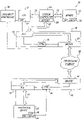
- FIG. 1 is a block diagram that schematically illustrates a computing system based on a packet-switching fabric, in accordance with a preferred embodiment of the present invention
- FIG. 2 is a flow chart that schematically illustrates a method for transmitting data from a peripheral device to a CPU in the system of FIG. 1 , in accordance with a preferred embodiment of the present invention.
- FIG. 3 is a flow chart that schematically illustrates a method for processing data received by the CPU in the system of FIG. 1 , in accordance with a preferred embodiment of the present invention.
- FIG. 1 is a block diagram that schematically illustrates a computing system 20 built around a switching fabric 26 , in accordance with a preferred embodiment of the present invention.
- the switching fabric preferably comprises an InfiniBand fabric, as described in the Background of the Invention, and some of the terms used hereinbelow are specific to the InfiniBand architecture. It will be understood, however, that the system architecture and methods of communication described herein are in no way limited to InfiniBand, and that other switching fabrics, as are known in the art, may be configured to handle and convey interrupts in a similar manner.
- a CPU 21 is coupled to communicate via a system bus 52 with a system controller 24 and a system memory 22 , as is known in the art.
- the CPU comprises an Intel Pentium processor, and bus 52 is a proprietary bus used in conjunction with this processor,
- System controller 24 is coupled to a standard I/O bus 50 , such as a PCI bus, for the purpose of communicating with peripheral devices, such as I/O adapters of various types.
- peripheral device 25 is shown in FIG. 1 by way of example, but in practical applications, system 20 typically comprises multiple peripheral devices and, possibly, multiple CPUs.
- Peripheral device 25 includes an interrupt output 48 , which it asserts in order to gain the attention of the CPU,
- interrupt output 48 is connected directly to an interrupt controller 38 , such as an Intel 8259 device, which actuates an appropriate interrupt input 27 of CPU 21 when the interrupt is asserted.
- interrupt controller 38 such as an Intel 8259 device
- interrupt output 48 and input 27 are linked only through fabric 26 , as described hereinbelow.
- Bus 50 is coupled to fabric 26 by a host network interface unit 28 .
- This unit comprises a host channel adapter (HCA) 32 , which interfaces with bus 50 and converts data between packet and parallel forms.
- HCA host channel adapter
- the HCA may be designed to interface with system bus 52 .
- a switch 30 links the HCA to one or more core switches in the fabric.
- data in packets received by switch 30 from fabric 26 are passed through HCA 32 to bus 50 .
- An exception is made, however, for management packets, which are packets that carry a special header identifying themselves as such and including a local identifier (LID) address of either switch 30 or HCA 32 .
- LID local identifier
- switch and HCA are placed in a dedicated register of the switch or HCA, as appropriate, which then attempts to decode the instructions and carry them out.
- FSA fabric service agent
- a host interface unit controller 36 acts as the FSA in interface unit 28 .
- the controller preferably comprises a microprocessor with random access memory (RAM) for software code and data, communicates with HCA 32 and switch 30 .
- the controller may comprise a hard-wired hardware element or digital signal processor.
- HCA 32 or switch 30 receives a management packet that it cannot decode, it passes the packet to the controller.
- the controller decodes the packet, preferably based on suitable software stored in its code RAM. It then takes whatever action is called for by the packet, such as giving appropriate instructions to HCA 32 or switch 30 .
- the HCA receives an interrupt packet, as described below, the actions taken by controller 36 also include signaling interrupt controller 38 via an interrupt output of unit 28 , so as to actuate interrupt input 27 of CPU 21 .
- the unit preferably comprises multiple interrupt lines These lines can be actuated selectively by controller 36 so as to send multiple, different interrupts to CPU 21 depending on the content of interrupt packets received by the HCA. Alternatively or additionally, the different interrupt lines may be used to signal other host devices that are linked to bus 50 .
- Peripheral device 25 is coupled to fabric 26 by a target network interface unit 40 , similar in structure to unit 28 .
- a target channel adapter (TCA) 42 in unit 40 interfaces via an I/O bus 53 with device 25 .
- bus 53 comprises a PCI bus, like bus 50 .
- a switch 44 links the TCA to the switching fabric.
- a target unit controller 46 similar to controller 36 , acts as FSA to TCA 42 and switch 44 and also has a suitable input to receive signals from interrupt output 48 of device 25 .
- FIG. 2 is a flow chart that schematically illustrates a method by which target interface unit 40 processes and transmits data from peripheral device 25 to HCA 32 over fabric 26 , in accordance with a preferred embodiment of the present invention.
- device 25 writes data via bus 53 to TCA 42 , to be conveyed by direct memory access to memory 22 .
- the peripheral device assigns a priority to the data to be transmitted and informs the TCA of this priority.
- the TCA packetizes the data and sends it over fabric 26 to the address of HCA 32 , with the priority assigned by the peripheral device.
- a packet header instructs the HCA to write the data to memory 22 .
- the TCA negotiates with switch 44 and fabric 26 to assign a fixed route for all of the packets through the fabric.
- a route together with the priority of the packets, is referred to herein as a channel.
- InfiniBand specifies that packets travelling over the same channel are always kept in their original order.
- controller 46 constructs an interrupt packet containing the interrupt cause information, at an interrupt packet sending step 68 .
- the interrupt packet is a management packet addressed to the LID of HCA 32 . It is preferably sent by controller 46 over the same channel, or virtual lane, as the data packets, after the last of the data packets has been sent.
- the interrupt packet also identifies the data with which the interrupt is associated. As a result, when the interrupt packet arrives at its destination, controller 36 will be able to generate an interrupt to CPU 21 that is associated with the appropriate memo write, as described below. Controller 46 assures than interrupt packet is sent to the fabric after all of the data packets have already been accepted for sending. It thus ensures that HCA 32 will receive the interrupt packet only after it has received all of the data packets.
- controller 46 may delay sending the interrupt packet until TCA 42 receives an acknowledgment from memory 22 that it has received all of the data.
- This approach introduces additional delay before CPU 21 can receive and act upon the interrupt, but it obviates the need to ensure that the interrupt packet is routed over the same channel as the data packets.
- Such an approach may be called for in particular when switching fabric 26 comprises a network in which consistent routing and ordering are not necessarily maintained among successive packets.
- This approach can also be used when the interrupt path and data path are not the same, and fork at an earlier stage than in FIG. 1 .
- Such path incongruity may occur, for example, when the device writing data to the memory is different from the device asserting the interrupt to the CPU.
- it is also desirable to send interrupts on different (high-priority) routes because data routes can be congested, causing interrupt messages to get stuck behind data.
- FIG. 3 is a flow chart that schematically illustrates a method by which data and accompanying interrupt packets are received and processed by host interface unit 28 and CPU 21 , in accordance with a preferred embodiment of the present invention.
- HCA 32 receives the data and interrupt packets sent from target interface unit 40 .
- the HCA posts the data in the data packets via bus 50 to a buffer 58 of system controller 24 .
- the system controller proceeds to write the data from its buffer to the appropriate addresses in memory 22 , as is known in the art.
- the HCA passes the interrupt packet to controller 36 for decoding, at an interrupt processing step 72 .
- the controller extracts the cause of the interrupt and posts this information, via HCA 32 , to an interrupt cause register 56 in memory 22 .
- controller 46 of target interface unit 40 is programmed to send the interrupt packet only after receiving the acknowledgment from memory 22 , as described above, this problem is already solved. Otherwise, controller 36 preferably waits to assert the interrupt until system controller 24 has acknowledged to HCA 32 that it has received all of the data. In response to this acknowledgment, controller 36 sends an interrupt signal to interrupt controller 38 , at an interrupt assertion step 76 .
- the interrupt controller actuates interrupt input 27 of CPU 21 , to inform the CPU that an interrupt has arrived from HCA 32 .
- the CPU preferably sends a dummy read command to the HCA, in order to ensure that buffer 58 is flushed to memory 22 before the CPU itself begins to process the data in the memory.
- controller 36 may send the interrupt signal to interrupt controller 38 immediately, without waiting for an acknowledgment from system controller 24 .
- CPU 21 preferably sends a “fence” command to HCA 32 . This command instructs the HCA to mark the last packet currently in its receive queue, and to inform the CPU when this last packet has been written to system controller 24 . At this point, the CPU can send its dummy read command and begin processing the data in the memory.
- CPU 21 reads the cause of the current interrupt from register 56 , at a cause reading step 78 . Based on this information, the CPU processes the data that peripheral device 25 has placed in the memory, at a data processing step 80 . Unlike methods of interrupt processing known in the art, all of the steps in the method of FIG. 3 are carried out locally, typically over busses 50 and 52 , without the need for messages to traverse fabric 26 .
Abstract
Description
-
- receiving data from a peripheral device for transmission via the network to a memory associated with a central processing unit (CPU);
- receiving an interrupt signal from the peripheral device associated with the data;
- sending one or more data packets containing the data over the network to a host network interface serving the memory and the CPU; and
- sending an interrupt packet over the network to the host network interface, responsive to which an interrupt input of the CPU is asserted only after the one or more data packets have arrived at the host network interface.
-
- receiving the data packets and the interrupt packet at the host network interface;
- conveying the data in the packets for delivery to the memory over a local bus coupling the host network interface to the memory and the CPU; and
- notifying the CPU when all of the data have been conveyed.
-
- a target channel adapter, which is operative to receive data from a peripheral device for transmission via a packet-switching network to a memory associated with a central processing unit (CPU) and to send one or more data packets containing the data over the network to a host network interface serving the memory and the CPU; and
- a target interface processor, adapted to receive an interrupt signal from the peripheral device associated with the data, and to send an interrupt packet over the network to the host network interface, responsive to which an interrupt input of the CPU is asserted only after the one or more data packets have arrived at the host network interface.
-
- a host channel adapter, which is operative to receive data packets transmitted over a packet-switching network from a peripheral device, and to convey data from the packets for delivery to a memory associated with a CPU over a local bus that is coupled to the memory and the CPU, and further to receive an interrupt packet sent over the network responsive to an interrupt signal asserted by the peripheral device after sending the data to the network; and
- a host interface processor, adapted, responsive to the interrupt packet, to notify the CPU when all of the data have been conveyed to the local bus.
Claims (10)
Priority Applications (1)
| Application Number | Priority Date | Filing Date | Title |
|---|---|---|---|
| US10/070,594 US6978331B1 (en) | 1999-09-08 | 2000-09-07 | Synchronization of interrupts with data packets |
Applications Claiming Priority (5)
| Application Number | Priority Date | Filing Date | Title |
|---|---|---|---|
| US15284999P | 1999-09-08 | 1999-09-08 | |
| US17533900P | 2000-01-10 | 2000-01-10 | |
| US09/559,352 US6243787B1 (en) | 2000-04-27 | 2000-04-27 | Synchronization of interrupts with data pockets |
| US10/070,594 US6978331B1 (en) | 1999-09-08 | 2000-09-07 | Synchronization of interrupts with data packets |
| PCT/IL2000/000540 WO2001018654A1 (en) | 1999-09-08 | 2000-09-07 | Synchronization of interrupts with data packets |
Publications (1)
| Publication Number | Publication Date |
|---|---|
| US6978331B1 true US6978331B1 (en) | 2005-12-20 |
Family
ID=27387331
Family Applications (1)
| Application Number | Title | Priority Date | Filing Date |
|---|---|---|---|
| US10/070,594 Expired - Lifetime US6978331B1 (en) | 1999-09-08 | 2000-09-07 | Synchronization of interrupts with data packets |
Country Status (4)
| Country | Link |
|---|---|
| US (1) | US6978331B1 (en) |
| AU (2) | AU7036300A (en) |
| IL (1) | IL148263A0 (en) |
| WO (2) | WO2001018654A1 (en) |
Cited By (44)
| Publication number | Priority date | Publication date | Assignee | Title |
|---|---|---|---|---|
| US20090216930A1 (en) * | 2008-02-27 | 2009-08-27 | Fujitsu Limited | Information processing apparatus and control method thereof |
| US20100049876A1 (en) * | 2005-04-27 | 2010-02-25 | Solarflare Communications, Inc. | Packet validation in virtual network interface architecture |
| US20100057932A1 (en) * | 2006-07-10 | 2010-03-04 | Solarflare Communications Incorporated | Onload network protocol stacks |
| US20100135324A1 (en) * | 2006-11-01 | 2010-06-03 | Solarflare Communications Inc. | Driver level segmentation |
| US20100161847A1 (en) * | 2008-12-18 | 2010-06-24 | Solarflare Communications, Inc. | Virtualised interface functions |
| US20110023042A1 (en) * | 2008-02-05 | 2011-01-27 | Solarflare Communications Inc. | Scalable sockets |
| US20110029734A1 (en) * | 2009-07-29 | 2011-02-03 | Solarflare Communications Inc | Controller Integration |
| US20110087774A1 (en) * | 2009-10-08 | 2011-04-14 | Solarflare Communications Inc | Switching api |
| US20110149966A1 (en) * | 2009-12-21 | 2011-06-23 | Solarflare Communications Inc | Header Processing Engine |
| US20110173514A1 (en) * | 2003-03-03 | 2011-07-14 | Solarflare Communications, Inc. | Data protocol |
| US20110184687A1 (en) * | 2010-01-25 | 2011-07-28 | Advantest Corporation | Test apparatus and test method |
| US8533740B2 (en) | 2005-03-15 | 2013-09-10 | Solarflare Communications, Inc. | Data processing system with intercepting instructions |
| US8543729B2 (en) | 2007-11-29 | 2013-09-24 | Solarflare Communications, Inc. | Virtualised receive side scaling |
| US8612536B2 (en) | 2004-04-21 | 2013-12-17 | Solarflare Communications, Inc. | User-level stack |
| US8635353B2 (en) | 2005-06-15 | 2014-01-21 | Solarflare Communications, Inc. | Reception according to a data transfer protocol of data directed to any of a plurality of destination entities |
| US8650569B2 (en) | 2005-03-10 | 2014-02-11 | Solarflare Communications, Inc. | User-level re-initialization instruction interception |
| US8737431B2 (en) | 2004-04-21 | 2014-05-27 | Solarflare Communications, Inc. | Checking data integrity |
| US8763018B2 (en) | 2011-08-22 | 2014-06-24 | Solarflare Communications, Inc. | Modifying application behaviour |
| US8782642B2 (en) | 2005-03-15 | 2014-07-15 | Solarflare Communications, Inc. | Data processing system with data transmit capability |
| US8817784B2 (en) | 2006-02-08 | 2014-08-26 | Solarflare Communications, Inc. | Method and apparatus for multicast packet reception |
| US8855137B2 (en) | 2004-03-02 | 2014-10-07 | Solarflare Communications, Inc. | Dual-driver interface |
| US8868780B2 (en) | 2005-03-30 | 2014-10-21 | Solarflare Communications, Inc. | Data processing system with routing tables |
| US8954613B2 (en) | 2002-09-16 | 2015-02-10 | Solarflare Communications, Inc. | Network interface and protocol |
| US8959095B2 (en) | 2005-10-20 | 2015-02-17 | Solarflare Communications, Inc. | Hashing algorithm for network receive filtering |
| US8996644B2 (en) | 2010-12-09 | 2015-03-31 | Solarflare Communications, Inc. | Encapsulated accelerator |
| US9003053B2 (en) | 2011-09-22 | 2015-04-07 | Solarflare Communications, Inc. | Message acceleration |
| US9008113B2 (en) | 2010-12-20 | 2015-04-14 | Solarflare Communications, Inc. | Mapped FIFO buffering |
| US20150127865A1 (en) * | 2013-11-07 | 2015-05-07 | Stmicroelectronics (Research & Development) Limited | Method and apparatus use with interrupts |
| US9210140B2 (en) | 2009-08-19 | 2015-12-08 | Solarflare Communications, Inc. | Remote functionality selection |
| US9258390B2 (en) | 2011-07-29 | 2016-02-09 | Solarflare Communications, Inc. | Reducing network latency |
| US9300599B2 (en) | 2013-05-30 | 2016-03-29 | Solarflare Communications, Inc. | Packet capture |
| US9384071B2 (en) | 2011-03-31 | 2016-07-05 | Solarflare Communications, Inc. | Epoll optimisations |
| US9391840B2 (en) | 2012-05-02 | 2016-07-12 | Solarflare Communications, Inc. | Avoiding delayed data |
| US9391841B2 (en) | 2012-07-03 | 2016-07-12 | Solarflare Communications, Inc. | Fast linkup arbitration |
| US9426124B2 (en) | 2013-04-08 | 2016-08-23 | Solarflare Communications, Inc. | Locked down network interface |
| US9600429B2 (en) | 2010-12-09 | 2017-03-21 | Solarflare Communications, Inc. | Encapsulated accelerator |
| US9674318B2 (en) | 2010-12-09 | 2017-06-06 | Solarflare Communications, Inc. | TCP processing for devices |
| US9686117B2 (en) | 2006-07-10 | 2017-06-20 | Solarflare Communications, Inc. | Chimney onload implementation of network protocol stack |
| US9948533B2 (en) | 2006-07-10 | 2018-04-17 | Solarflare Communitations, Inc. | Interrupt management |
| US10015104B2 (en) | 2005-12-28 | 2018-07-03 | Solarflare Communications, Inc. | Processing received data |
| US10394751B2 (en) | 2013-11-06 | 2019-08-27 | Solarflare Communications, Inc. | Programmed input/output mode |
| US10505747B2 (en) | 2012-10-16 | 2019-12-10 | Solarflare Communications, Inc. | Feed processing |
| US10742604B2 (en) | 2013-04-08 | 2020-08-11 | Xilinx, Inc. | Locked down network interface |
| US10873613B2 (en) | 2010-12-09 | 2020-12-22 | Xilinx, Inc. | TCP processing for devices |
Families Citing this family (4)
| Publication number | Priority date | Publication date | Assignee | Title |
|---|---|---|---|---|
| US6836813B1 (en) * | 2001-11-30 | 2004-12-28 | Advanced Micro Devices, Inc. | Switching I/O node for connection in a multiprocessor computer system |
| US6928508B2 (en) | 2002-09-12 | 2005-08-09 | Sun Microsystems, Inc. | Method of accessing a remote device from a host by mapping an address of the device to a memory address of the host |
| US7243173B2 (en) | 2004-12-14 | 2007-07-10 | Rockwell Automation Technologies, Inc. | Low protocol, high speed serial transfer for intra-board or inter-board data communication |
| US9760514B1 (en) | 2016-09-26 | 2017-09-12 | International Business Machines Corporation | Multi-packet processing with ordering rule enforcement |
Citations (11)
| Publication number | Priority date | Publication date | Assignee | Title |
|---|---|---|---|---|
| US5440545A (en) | 1993-08-02 | 1995-08-08 | Motorola, Inc. | Packet delivery system |
| US5519700A (en) | 1994-12-07 | 1996-05-21 | At&T Corp. | Telecommunication system with synchronous-asynchronous interface |
| US5659758A (en) | 1995-07-07 | 1997-08-19 | Sun Microsystems, Inc. | Interrupt modular for receiving bursty high speed network traffic |
| US5689713A (en) | 1995-03-31 | 1997-11-18 | Sun Microsystems, Inc. | Method and apparatus for interrupt communication in a packet-switched computer system |
| US5754550A (en) | 1994-05-23 | 1998-05-19 | Nec Corporation | System data transfer through a fixed path in a switching system |
| US5898669A (en) | 1996-03-22 | 1999-04-27 | Shimony; Ilan | ATM traffic management device |
| US6038629A (en) | 1996-10-15 | 2000-03-14 | International Business Machines Corporation | Computer system generating a processor interrupt in response to receiving an interrupt/data synchronizing signal over a data bus |
| US6243787B1 (en) * | 2000-04-27 | 2001-06-05 | Mellanox Technologies Ltd. | Synchronization of interrupts with data pockets |
| US6295573B1 (en) * | 1999-02-16 | 2001-09-25 | Advanced Micro Devices, Inc. | Point-to-point interrupt messaging within a multiprocessing computer system |
| US6549965B1 (en) * | 1998-04-29 | 2003-04-15 | Stmicroelectronics Limited | Microcomputer with interrupt packets |
| US6604161B1 (en) * | 1999-09-29 | 2003-08-05 | Silicon Graphics, Inc. | Translation of PCI level interrupts into packet based messages for edge event drive microprocessors |
Family Cites Families (3)
| Publication number | Priority date | Publication date | Assignee | Title |
|---|---|---|---|---|
| US5764895A (en) * | 1995-01-11 | 1998-06-09 | Sony Corporation | Method and apparatus for directing data packets in a local area network device having a plurality of ports interconnected by a high-speed communication bus |
| US6141351A (en) * | 1996-12-20 | 2000-10-31 | International Business Machines Corporation | Radio frequency bus for broadband microprocessor communications |
| US5920698A (en) * | 1997-01-06 | 1999-07-06 | Digital Equipment Corporation | Automatic detection of a similar device at the other end of a wire in a computer network |
-
2000
- 2000-09-07 AU AU70363/00A patent/AU7036300A/en not_active Abandoned
- 2000-09-07 IL IL14826300A patent/IL148263A0/en unknown
- 2000-09-07 WO PCT/IL2000/000540 patent/WO2001018654A1/en active Application Filing
- 2000-09-07 US US10/070,594 patent/US6978331B1/en not_active Expired - Lifetime
- 2000-09-07 AU AU70364/00A patent/AU7036400A/en not_active Abandoned
- 2000-09-07 WO PCT/IL2000/000538 patent/WO2001018988A1/en active Application Filing
Patent Citations (11)
| Publication number | Priority date | Publication date | Assignee | Title |
|---|---|---|---|---|
| US5440545A (en) | 1993-08-02 | 1995-08-08 | Motorola, Inc. | Packet delivery system |
| US5754550A (en) | 1994-05-23 | 1998-05-19 | Nec Corporation | System data transfer through a fixed path in a switching system |
| US5519700A (en) | 1994-12-07 | 1996-05-21 | At&T Corp. | Telecommunication system with synchronous-asynchronous interface |
| US5689713A (en) | 1995-03-31 | 1997-11-18 | Sun Microsystems, Inc. | Method and apparatus for interrupt communication in a packet-switched computer system |
| US5659758A (en) | 1995-07-07 | 1997-08-19 | Sun Microsystems, Inc. | Interrupt modular for receiving bursty high speed network traffic |
| US5898669A (en) | 1996-03-22 | 1999-04-27 | Shimony; Ilan | ATM traffic management device |
| US6038629A (en) | 1996-10-15 | 2000-03-14 | International Business Machines Corporation | Computer system generating a processor interrupt in response to receiving an interrupt/data synchronizing signal over a data bus |
| US6549965B1 (en) * | 1998-04-29 | 2003-04-15 | Stmicroelectronics Limited | Microcomputer with interrupt packets |
| US6295573B1 (en) * | 1999-02-16 | 2001-09-25 | Advanced Micro Devices, Inc. | Point-to-point interrupt messaging within a multiprocessing computer system |
| US6604161B1 (en) * | 1999-09-29 | 2003-08-05 | Silicon Graphics, Inc. | Translation of PCI level interrupts into packet based messages for edge event drive microprocessors |
| US6243787B1 (en) * | 2000-04-27 | 2001-06-05 | Mellanox Technologies Ltd. | Synchronization of interrupts with data pockets |
Cited By (103)
| Publication number | Priority date | Publication date | Assignee | Title |
|---|---|---|---|---|
| US8954613B2 (en) | 2002-09-16 | 2015-02-10 | Solarflare Communications, Inc. | Network interface and protocol |
| US9112752B2 (en) | 2002-09-16 | 2015-08-18 | Solarflare Communications, Inc. | Network interface and protocol |
| US9043671B2 (en) | 2003-03-03 | 2015-05-26 | Solarflare Communications, Inc. | Data protocol |
| US20110173514A1 (en) * | 2003-03-03 | 2011-07-14 | Solarflare Communications, Inc. | Data protocol |
| US8855137B2 (en) | 2004-03-02 | 2014-10-07 | Solarflare Communications, Inc. | Dual-driver interface |
| US11182317B2 (en) | 2004-03-02 | 2021-11-23 | Xilinx, Inc. | Dual-driver interface |
| US11119956B2 (en) | 2004-03-02 | 2021-09-14 | Xilinx, Inc. | Dual-driver interface |
| US9690724B2 (en) | 2004-03-02 | 2017-06-27 | Solarflare Communications, Inc. | Dual-driver interface |
| US8612536B2 (en) | 2004-04-21 | 2013-12-17 | Solarflare Communications, Inc. | User-level stack |
| US8737431B2 (en) | 2004-04-21 | 2014-05-27 | Solarflare Communications, Inc. | Checking data integrity |
| US8650569B2 (en) | 2005-03-10 | 2014-02-11 | Solarflare Communications, Inc. | User-level re-initialization instruction interception |
| US9063771B2 (en) | 2005-03-10 | 2015-06-23 | Solarflare Communications, Inc. | User-level re-initialization instruction interception |
| US8782642B2 (en) | 2005-03-15 | 2014-07-15 | Solarflare Communications, Inc. | Data processing system with data transmit capability |
| US9552225B2 (en) | 2005-03-15 | 2017-01-24 | Solarflare Communications, Inc. | Data processing system with data transmit capability |
| US8533740B2 (en) | 2005-03-15 | 2013-09-10 | Solarflare Communications, Inc. | Data processing system with intercepting instructions |
| US10397103B2 (en) | 2005-03-30 | 2019-08-27 | Solarflare Communications, Inc. | Data processing system with routing tables |
| US9729436B2 (en) | 2005-03-30 | 2017-08-08 | Solarflare Communications, Inc. | Data processing system with routing tables |
| US8868780B2 (en) | 2005-03-30 | 2014-10-21 | Solarflare Communications, Inc. | Data processing system with routing tables |
| US9912665B2 (en) | 2005-04-27 | 2018-03-06 | Solarflare Communications, Inc. | Packet validation in virtual network interface architecture |
| US8380882B2 (en) | 2005-04-27 | 2013-02-19 | Solarflare Communications, Inc. | Packet validation in virtual network interface architecture |
| US10924483B2 (en) | 2005-04-27 | 2021-02-16 | Xilinx, Inc. | Packet validation in virtual network interface architecture |
| US20100049876A1 (en) * | 2005-04-27 | 2010-02-25 | Solarflare Communications, Inc. | Packet validation in virtual network interface architecture |
| US9043380B2 (en) | 2005-06-15 | 2015-05-26 | Solarflare Communications, Inc. | Reception according to a data transfer protocol of data directed to any of a plurality of destination entities |
| US8645558B2 (en) | 2005-06-15 | 2014-02-04 | Solarflare Communications, Inc. | Reception according to a data transfer protocol of data directed to any of a plurality of destination entities for data extraction |
| US8635353B2 (en) | 2005-06-15 | 2014-01-21 | Solarflare Communications, Inc. | Reception according to a data transfer protocol of data directed to any of a plurality of destination entities |
| US10055264B2 (en) | 2005-06-15 | 2018-08-21 | Solarflare Communications, Inc. | Reception according to a data transfer protocol of data directed to any of a plurality of destination entities |
| US10445156B2 (en) | 2005-06-15 | 2019-10-15 | Solarflare Communications, Inc. | Reception according to a data transfer protocol of data directed to any of a plurality of destination entities |
| US11210148B2 (en) | 2005-06-15 | 2021-12-28 | Xilinx, Inc. | Reception according to a data transfer protocol of data directed to any of a plurality of destination entities |
| US9594842B2 (en) | 2005-10-20 | 2017-03-14 | Solarflare Communications, Inc. | Hashing algorithm for network receive filtering |
| US8959095B2 (en) | 2005-10-20 | 2015-02-17 | Solarflare Communications, Inc. | Hashing algorithm for network receive filtering |
| US10015104B2 (en) | 2005-12-28 | 2018-07-03 | Solarflare Communications, Inc. | Processing received data |
| US10104005B2 (en) | 2006-01-10 | 2018-10-16 | Solarflare Communications, Inc. | Data buffering |
| US8817784B2 (en) | 2006-02-08 | 2014-08-26 | Solarflare Communications, Inc. | Method and apparatus for multicast packet reception |
| US9083539B2 (en) | 2006-02-08 | 2015-07-14 | Solarflare Communications, Inc. | Method and apparatus for multicast packet reception |
| US10382248B2 (en) | 2006-07-10 | 2019-08-13 | Solarflare Communications, Inc. | Chimney onload implementation of network protocol stack |
| US20100057932A1 (en) * | 2006-07-10 | 2010-03-04 | Solarflare Communications Incorporated | Onload network protocol stacks |
| US9948533B2 (en) | 2006-07-10 | 2018-04-17 | Solarflare Communitations, Inc. | Interrupt management |
| US9686117B2 (en) | 2006-07-10 | 2017-06-20 | Solarflare Communications, Inc. | Chimney onload implementation of network protocol stack |
| US8489761B2 (en) | 2006-07-10 | 2013-07-16 | Solarflare Communications, Inc. | Onload network protocol stacks |
| US20100135324A1 (en) * | 2006-11-01 | 2010-06-03 | Solarflare Communications Inc. | Driver level segmentation |
| US9077751B2 (en) | 2006-11-01 | 2015-07-07 | Solarflare Communications, Inc. | Driver level segmentation |
| US8543729B2 (en) | 2007-11-29 | 2013-09-24 | Solarflare Communications, Inc. | Virtualised receive side scaling |
| US20110023042A1 (en) * | 2008-02-05 | 2011-01-27 | Solarflare Communications Inc. | Scalable sockets |
| US9304825B2 (en) | 2008-02-05 | 2016-04-05 | Solarflare Communications, Inc. | Processing, on multiple processors, data flows received through a single socket |
| CN101520758A (en) * | 2008-02-27 | 2009-09-02 | 富士通株式会社 | Information processing apparatus and control method thereof |
| US8151028B2 (en) * | 2008-02-27 | 2012-04-03 | Fujitsu Limited | Information processing apparatus and control method thereof |
| KR101056759B1 (en) | 2008-02-27 | 2011-08-16 | 후지쯔 가부시끼가이샤 | Recording medium recording an information processing system, a method of controlling the information processing system, and a control program of the information processing system |
| US20090216930A1 (en) * | 2008-02-27 | 2009-08-27 | Fujitsu Limited | Information processing apparatus and control method thereof |
| US8447904B2 (en) | 2008-12-18 | 2013-05-21 | Solarflare Communications, Inc. | Virtualised interface functions |
| US20100161847A1 (en) * | 2008-12-18 | 2010-06-24 | Solarflare Communications, Inc. | Virtualised interface functions |
| US9256560B2 (en) | 2009-07-29 | 2016-02-09 | Solarflare Communications, Inc. | Controller integration |
| US20110029734A1 (en) * | 2009-07-29 | 2011-02-03 | Solarflare Communications Inc | Controller Integration |
| US9210140B2 (en) | 2009-08-19 | 2015-12-08 | Solarflare Communications, Inc. | Remote functionality selection |
| US8423639B2 (en) | 2009-10-08 | 2013-04-16 | Solarflare Communications, Inc. | Switching API |
| US20110087774A1 (en) * | 2009-10-08 | 2011-04-14 | Solarflare Communications Inc | Switching api |
| US8743877B2 (en) | 2009-12-21 | 2014-06-03 | Steven L. Pope | Header processing engine |
| US20110149966A1 (en) * | 2009-12-21 | 2011-06-23 | Solarflare Communications Inc | Header Processing Engine |
| US9124539B2 (en) | 2009-12-21 | 2015-09-01 | Solarflare Communications, Inc. | Header processing engine |
| US20110184687A1 (en) * | 2010-01-25 | 2011-07-28 | Advantest Corporation | Test apparatus and test method |
| CN102193056A (en) * | 2010-01-25 | 2011-09-21 | 爱德万测试株式会社 | Test apparatus and test method |
| US8996644B2 (en) | 2010-12-09 | 2015-03-31 | Solarflare Communications, Inc. | Encapsulated accelerator |
| US9600429B2 (en) | 2010-12-09 | 2017-03-21 | Solarflare Communications, Inc. | Encapsulated accelerator |
| US10515037B2 (en) | 2010-12-09 | 2019-12-24 | Solarflare Communications, Inc. | Encapsulated accelerator |
| US9880964B2 (en) | 2010-12-09 | 2018-01-30 | Solarflare Communications, Inc. | Encapsulated accelerator |
| US9892082B2 (en) | 2010-12-09 | 2018-02-13 | Solarflare Communications Inc. | Encapsulated accelerator |
| US11132317B2 (en) | 2010-12-09 | 2021-09-28 | Xilinx, Inc. | Encapsulated accelerator |
| US11876880B2 (en) | 2010-12-09 | 2024-01-16 | Xilinx, Inc. | TCP processing for devices |
| US10572417B2 (en) | 2010-12-09 | 2020-02-25 | Xilinx, Inc. | Encapsulated accelerator |
| US11134140B2 (en) | 2010-12-09 | 2021-09-28 | Xilinx, Inc. | TCP processing for devices |
| US9674318B2 (en) | 2010-12-09 | 2017-06-06 | Solarflare Communications, Inc. | TCP processing for devices |
| US10873613B2 (en) | 2010-12-09 | 2020-12-22 | Xilinx, Inc. | TCP processing for devices |
| US9800513B2 (en) | 2010-12-20 | 2017-10-24 | Solarflare Communications, Inc. | Mapped FIFO buffering |
| US9008113B2 (en) | 2010-12-20 | 2015-04-14 | Solarflare Communications, Inc. | Mapped FIFO buffering |
| US10671458B2 (en) | 2011-03-31 | 2020-06-02 | Xilinx, Inc. | Epoll optimisations |
| US9384071B2 (en) | 2011-03-31 | 2016-07-05 | Solarflare Communications, Inc. | Epoll optimisations |
| US9258390B2 (en) | 2011-07-29 | 2016-02-09 | Solarflare Communications, Inc. | Reducing network latency |
| US10425512B2 (en) | 2011-07-29 | 2019-09-24 | Solarflare Communications, Inc. | Reducing network latency |
| US10469632B2 (en) | 2011-07-29 | 2019-11-05 | Solarflare Communications, Inc. | Reducing network latency |
| US10021223B2 (en) | 2011-07-29 | 2018-07-10 | Solarflare Communications, Inc. | Reducing network latency |
| US9456060B2 (en) | 2011-07-29 | 2016-09-27 | Solarflare Communications, Inc. | Reducing network latency |
| US10713099B2 (en) | 2011-08-22 | 2020-07-14 | Xilinx, Inc. | Modifying application behaviour |
| US11392429B2 (en) | 2011-08-22 | 2022-07-19 | Xilinx, Inc. | Modifying application behaviour |
| US8763018B2 (en) | 2011-08-22 | 2014-06-24 | Solarflare Communications, Inc. | Modifying application behaviour |
| US9003053B2 (en) | 2011-09-22 | 2015-04-07 | Solarflare Communications, Inc. | Message acceleration |
| US9391840B2 (en) | 2012-05-02 | 2016-07-12 | Solarflare Communications, Inc. | Avoiding delayed data |
| US11108633B2 (en) | 2012-07-03 | 2021-08-31 | Xilinx, Inc. | Protocol selection in dependence upon conversion time |
| US10498602B2 (en) | 2012-07-03 | 2019-12-03 | Solarflare Communications, Inc. | Fast linkup arbitration |
| US9882781B2 (en) | 2012-07-03 | 2018-01-30 | Solarflare Communications, Inc. | Fast linkup arbitration |
| US9391841B2 (en) | 2012-07-03 | 2016-07-12 | Solarflare Communications, Inc. | Fast linkup arbitration |
| US11095515B2 (en) | 2012-07-03 | 2021-08-17 | Xilinx, Inc. | Using receive timestamps to update latency estimates |
| US11374777B2 (en) | 2012-10-16 | 2022-06-28 | Xilinx, Inc. | Feed processing |
| US10505747B2 (en) | 2012-10-16 | 2019-12-10 | Solarflare Communications, Inc. | Feed processing |
| US10742604B2 (en) | 2013-04-08 | 2020-08-11 | Xilinx, Inc. | Locked down network interface |
| US9426124B2 (en) | 2013-04-08 | 2016-08-23 | Solarflare Communications, Inc. | Locked down network interface |
| US10999246B2 (en) | 2013-04-08 | 2021-05-04 | Xilinx, Inc. | Locked down network interface |
| US10212135B2 (en) | 2013-04-08 | 2019-02-19 | Solarflare Communications, Inc. | Locked down network interface |
| US9300599B2 (en) | 2013-05-30 | 2016-03-29 | Solarflare Communications, Inc. | Packet capture |
| US11023411B2 (en) | 2013-11-06 | 2021-06-01 | Xilinx, Inc. | Programmed input/output mode |
| US11249938B2 (en) | 2013-11-06 | 2022-02-15 | Xilinx, Inc. | Programmed input/output mode |
| US10394751B2 (en) | 2013-11-06 | 2019-08-27 | Solarflare Communications, Inc. | Programmed input/output mode |
| US11809367B2 (en) | 2013-11-06 | 2023-11-07 | Xilinx, Inc. | Programmed input/output mode |
| US10255207B2 (en) * | 2013-11-07 | 2019-04-09 | Stmicroelectronics (Research & Development) Limited | Method and apparatus use with interrupts |
| US20150127865A1 (en) * | 2013-11-07 | 2015-05-07 | Stmicroelectronics (Research & Development) Limited | Method and apparatus use with interrupts |
Also Published As
| Publication number | Publication date |
|---|---|
| AU7036400A (en) | 2001-04-10 |
| IL148263A0 (en) | 2002-09-12 |
| WO2001018654A1 (en) | 2001-03-15 |
| WO2001018988A1 (en) | 2001-03-15 |
| AU7036300A (en) | 2001-04-10 |
Similar Documents
| Publication | Publication Date | Title |
|---|---|---|
| US6978331B1 (en) | Synchronization of interrupts with data packets | |
| US6243787B1 (en) | Synchronization of interrupts with data pockets | |
| US20220197831A1 (en) | System and method for facilitating efficient host memory access from a network interface controller (nic) | |
| US7281030B1 (en) | Method of reading a remote memory | |
| EP0255091B1 (en) | Multi-CPU interlock | |
| EP0257348B1 (en) | Multiprocessor interrupt rerouting mechanism | |
| US5187780A (en) | Dual-path computer interconnect system with zone manager for packet memory | |
| US5020020A (en) | Computer interconnect system with transmit-abort function | |
| US4744078A (en) | Multiple path multiplexed host to network data communication system | |
| US20040252685A1 (en) | Channel adapter with integrated switch | |
| EP0747831A2 (en) | Data processing system including buffering mechanism for inbound and outbound reads and posted writes | |
| US20060129699A1 (en) | Network interface adapter with shared data send resources | |
| KR20050039859A (en) | Store and forward switch device, system and method | |
| US20040024948A1 (en) | Response reordering mechanism | |
| US6694392B1 (en) | Transaction partitioning | |
| JPH06511338A (en) | Method and apparatus for parallel packet bus | |
| US5978865A (en) | System for performing DMA transfers where an interrupt request signal is generated based on the value of the last of a plurality of data bits transmitted | |
| US7181561B2 (en) | Ordering rule controlled command storage | |
| US6256699B1 (en) | Reliable interrupt reception over buffered bus | |
| US20030043794A1 (en) | Data stream multiplexing in data network | |
| KR20000006114A (en) | Method and apparatus for providing a network interface | |
| EP1815663B1 (en) | Performance based packet ordering in a pci express bus | |
| KR100412010B1 (en) | Flow architecture for remote high-speed interface application | |
| WO2001067713A1 (en) | A packet format independent computer network controller | |
| US7577774B2 (en) | Independent source read and destination write enhanced DMA |
Legal Events
| Date | Code | Title | Description |
|---|---|---|---|
| AS | Assignment |
Owner name: MELLANOX TECHNOLOGIES LTD., ISRAEL Free format text: ASSIGNMENT OF ASSIGNORS INTEREST;ASSIGNORS:KAGAN, MICHAEL;CRUPNICOFF, DIEGO;GABBAY, FREDDY;AND OTHERS;REEL/FRAME:013264/0880;SIGNING DATES FROM 20020625 TO 20020703 |
|
| STCF | Information on status: patent grant |
Free format text: PATENTED CASE |
|
| FPAY | Fee payment |
Year of fee payment: 4 |
|
| FEPP | Fee payment procedure |
Free format text: PAT HOLDER NO LONGER CLAIMS SMALL ENTITY STATUS, ENTITY STATUS SET TO UNDISCOUNTED (ORIGINAL EVENT CODE: STOL); ENTITY STATUS OF PATENT OWNER: LARGE ENTITY |
|
| FPAY | Fee payment |
Year of fee payment: 8 |
|
| FEPP | Fee payment procedure |
Free format text: PAYER NUMBER DE-ASSIGNED (ORIGINAL EVENT CODE: RMPN); ENTITY STATUS OF PATENT OWNER: LARGE ENTITY Free format text: PAYOR NUMBER ASSIGNED (ORIGINAL EVENT CODE: ASPN); ENTITY STATUS OF PATENT OWNER: LARGE ENTITY |
|
| AS | Assignment |
Owner name: JPMORGAN CHASE BANK, N.A., AS ADMINISTRATIVE AGENT, ILLINOIS Free format text: PATENT SECURITY AGREEMENT;ASSIGNOR:MELLANOX TECHNOLOGIES, LTD.;REEL/FRAME:037900/0720 Effective date: 20160222 Owner name: JPMORGAN CHASE BANK, N.A., AS ADMINISTRATIVE AGENT Free format text: PATENT SECURITY AGREEMENT;ASSIGNOR:MELLANOX TECHNOLOGIES, LTD.;REEL/FRAME:037900/0720 Effective date: 20160222 |
|
| FPAY | Fee payment |
Year of fee payment: 12 |
|
| AS | Assignment |
Owner name: MELLANOX TECHNOLOGIES, LTD., ISRAEL Free format text: RELEASE OF SECURITY INTEREST IN PATENT COLLATERAL AT REEL/FRAME NO. 37900/0720;ASSIGNOR:JPMORGAN CHASE BANK, N.A., AS ADMINISTRATIVE AGENT;REEL/FRAME:046542/0792 Effective date: 20180709 |