US6993630B1 - Data pre-fetch system and method for a cache memory - Google Patents
Data pre-fetch system and method for a cache memory Download PDFInfo
- Publication number
- US6993630B1 US6993630B1 US10/255,393 US25539302A US6993630B1 US 6993630 B1 US6993630 B1 US 6993630B1 US 25539302 A US25539302 A US 25539302A US 6993630 B1 US6993630 B1 US 6993630B1
- Authority
- US
- United States
- Prior art keywords
- cache
- fetch
- data
- request
- requests
- Prior art date
- Legal status (The legal status is an assumption and is not a legal conclusion. Google has not performed a legal analysis and makes no representation as to the accuracy of the status listed.)
- Expired - Fee Related, expires
Links
Images


Classifications
-
- G—PHYSICS
- G06—COMPUTING; CALCULATING OR COUNTING
- G06F—ELECTRIC DIGITAL DATA PROCESSING
- G06F12/00—Accessing, addressing or allocating within memory systems or architectures
- G06F12/02—Addressing or allocation; Relocation
- G06F12/08—Addressing or allocation; Relocation in hierarchically structured memory systems, e.g. virtual memory systems
- G06F12/0802—Addressing of a memory level in which the access to the desired data or data block requires associative addressing means, e.g. caches
- G06F12/0862—Addressing of a memory level in which the access to the desired data or data block requires associative addressing means, e.g. caches with prefetch
-
- G—PHYSICS
- G06—COMPUTING; CALCULATING OR COUNTING
- G06F—ELECTRIC DIGITAL DATA PROCESSING
- G06F2212/00—Indexing scheme relating to accessing, addressing or allocation within memory systems or architectures
- G06F2212/10—Providing a specific technical effect
- G06F2212/1016—Performance improvement
- G06F2212/1024—Latency reduction
Definitions
- This invention relates generally to data processing systems, and more particularly to an improved system and method for pre-fetching data to be stored within a cache memory.
- U.S. Pat. No. 3,806,888 issued to Brickman et al shows an early data processing system employing a cache memory residing between the main memory and the instruction processor, or central processing unit. In this system, real memory is segmented into blocks or pages. If the instruction processor requests access to one data element of a block, the entire block is automatically transferred to the cache memory for subsequent use by the instruction processor.
- U.S. Pat. No. 4,225,922 issued to Porter attempts to improve upon the basic cache approach by segmenting the cache memory and by buffering cache commands.
- U.S. Pat. No. 4,354,232 issued to Ryan also buffers cache control commands.
- the pre-fetching of data may be further complicated by variable length elements.
- U.S. Pat. No. 4,189,772 issued to Liptay attempts to address this problem by buffering the input to the cache memory.
- a decoder element is added by U.S. Pat. No. 4,437,149 issued to Pomerene et al, between the main memory and the cache memory to partially decode instructions before the cache memory is loaded.
- a multiprocessor system is shown in U.S. Pat. No. 5,023,776 issued to Gregor.
- the individual instruction processors have dedicated cache memories.
- Shared cache memories are interposed between the dedicated cache memories and the main memory.
- Write buffers are employed in parallel with the shared caches. Multiple sequential writes bypass the shared cache and proceed directly to the main memory through the write buffers.
- U.S. Pat. No. 5,423,016, issued to Tsuchiya et al. discloses a system that stores pre-fetched data elements in a block buffer before loading them into a cache memory. This load is accomplished beginning from the requested data element first such that as soon as the requested data element has been loaded into the block buffer, it is made available to the instruction processor. In this way, the instruction processor is permitted to execute subsequent instructions from cache memory, in parallel with loading of the remainder of the requested block of data into the block buffer. The instruction processor is able to obtain data from the cache memory because the cache memory is not busy storing the requested block.
- U.S. Pat. No. 5,724,533 to Kuslak et al. discloses a method and apparatus for efficiently halting the operation of the instruction processor when a cache miss is detected. Generally, this is accomplished by preventing unwanted address incrementation of an instruction address pipeline and by providing a null instruction to an instruction pipeline when a cache miss is detected. The system is adapted to eliminate a recovery period after the cache miss is handled.
- an Instruction Processor is coupled to a cache.
- IP Instruction Processor
- the pre-fetch control logic determines whether the data signals are available within the cache. If not, the data signals are retrieved from another memory within the data processing system, and are stored to the cache. If the associated request to access the data signals is provided to the cache after processing for the pre-fetch request has completed, the access request may be completed to the cache without resulting in a cache miss.
- multiple pre-fetch requests may be pending at once.
- the data may be stored to the cache without regard for the order in which the pre-fetch requests were issued.
- pre-fetch requests are provided to an interface that couples the cache to one or more other memories in the system.
- the rate at which these pre-fetch requests are provided to the interface may be programmably selected to match the rate at which the associated requests to access the data signals are provided to the cache. This throttles the pre-fetching logic so that a large time delay does not occur between the pre-fetch operation and a later data access. The chance that data will be fetched away by another processor within the system between completion of the pre-fetch operation and a later cache access is thereby minimized.
- the inventive system is programmable so that the user may select the way in which requests are throttled.
- the rate at which pre-fetch requests are issued may further be based on the type of data access request that is associated with the pre-fetch operation. For example, pre-fetch requests that are associated with some block write operations do not need to be throttled, since these operations pre-fetch data that is unlikely to be needed by another processor in the system.
- the IP is coupled to the cache memory via a primary interface and an auxiliary interface.
- an IP When an IP generates predetermined types of requests, some of the request data is provided over the auxiliary interface to pre-fetch control logic to initiate a pre-fetch operation.
- An associated request to access the data signals may be provided to the cache over the primary interface at substantially the same time.
- only predetermined types of requests are processed by pre-fetch control logic.
- only write requests result in the initiation of pre-fetch operations.
- a filter may be used to prevent certain requests from generating a pre-fetch request. For example, if two requests to the same address are received sequentially, only the first request results in initiation of a pre-fetch operation.
- the filter operates only if the two requests are received sequentially within a predetermined time period.
- the filter is programmable to select the mode of operation, and to further select the time delay between requests.
- a system for utilizing a cache memory includes a primary interface coupling the IP to the cache memory to provide requests from the IP to the cache memory.
- the system further includes an auxiliary interface coupling the IP to the cache memory to provide an address to the cache memory, whereby a pre-fetch operation may be initiated to obtain data signals identified by the address if the data signals are not stored in the cache memory.
- a method of utilizing a cache memory includes providing an address from an IP to the cache via an auxiliary interface to determine whether addressed data is resident in the cache.
- the method further comprises providing an request from the IP via a primary interface to access the cache.
- a system for processing requests within a data processing system includes a decode circuit within an IP for generating requests that include addresses.
- the system further includes pre-fetch logic coupled to the decode circuit to determine whether predetermined ones of the addresses are resident within the cache memory.
- Request interface logic that is coupled to the pre-fetch logic is provided to obtain data addressed by each of the predetermined ones of the addresses if the data is not resident within the cache memory.
- Cache control logic is coupled to the request interface logic to write obtained data to the cache memory irrespective of the order in which the requests were generated.
- a method of utilizing a cache memory includes the steps of generating one or more requests to access the cache memory, wherein each request includes an address.
- the method further includes scheduling the requests for processing by the cache memory. Independently of the scheduling step, it is determined whether ones of the addresses are resident within the cache memory. For each address that is not resident within the cache memory, the addressed data signals are obtained and stored in the cache memory.
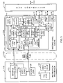
- FIG. 1 is a block diagram of an exemplary data processing system of the type that may employ the current invention.
- FIG. 2 is a block diagram of an exemplary prior art system for pre-fetching data.
- FIG. 3 is a block diagram of one embodiment of the current invention.
- FIG. 4 is a flow diagram of one process according to the current invention.
- FIG. 5 is a flow diagram illustrating one method of entering addresses into the pre-fetch storage device according to the current invention.
- FIG. 1 is a block diagram of an exemplary data processing system that may employ the current invention.
- the system includes a memory storage unit (MSU) 100 that provides the main memory facility for the system.
- MSU 100 may include random access memory (RAM), read-only memory (ROM), and any other type of memory known in the art.
- MSU 100 may be subdivided into multiple subunits (not shown) in a manner largely beyond the scope of the current invention.
- MSU is a directory-based storage unit similar to the system described in commonly-assigned U.S. Pat. No. 6,587,931 issued Jul. 1, 2003 to Bauman et al. entitled “Directory Based Cache Coherency System Supporting Multiple Instruction Processor and Input/Output Caches”, incorporated herein by reference.
- MSU retains information in directory 101 that indicates where the latest copy of requested data resides within the system. This is necessary since data from MSU 100 may be copied into any of the various cache memories within the system.
- Directory 101 tracks the latest copy of the data to ensure that every processor is operating from this copy.
- directory 101 includes a directory entry that tracks the location of each 128-byte block of memory within the MSU, where a 128-byte block is referred to as a cache line.
- MSU is coupled to one or more Storage Node Controllers (SNCs) shown as SNCs 102 A and 102 B.
- SNCs Storage Node Controllers
- the system of the current invention may include more or fewer SNCs than are shown in FIG. 1 .
- Each SNC is coupled to MSU 100 over one or more high-speed MSU interfaces that each includes data, address, and function lines. For simplicity, each SNC is shown coupled to MSU 100 over a single interface.
- Each SNC includes logic to interface to the high-speed MSU interface, and further includes logic to interface to a respective processor bus such as processor buses 104 A and 104 B. These processor buses can employ any type of bus protocol.
- Each SNC may further include a respective cache and all supporting logic. This cache may be a Third-Level Cache (TLC), a Fourth-Level Cache (4LC), or some other type of cache memory.
- SNCs 102 A and 102 B include TLCs 106 A and 106 B, respectively.
- each of SNCs 102 A and 102 B is coupled to a respective processor bus 104 A and 104 B.
- Each processor bus further couples to multiple local cache memories through respective Bus Controllers (BCs).
- BCs Bus Controllers
- Each BC controls the transfer of data to and from the processor bus in a manner that conforms to bus protocol.
- Second-Level Caches (SLCs) 108 A– 108 D are coupled to processor bus 104 A through BCs 114 A– 114 D, respectively.
- SLCs 108 E– 108 H are coupled to processor bus 104 B through BCs 114 E– 114 H, respectively.
- these local caches may be Third-Level Caches.
- Each SLC 108 is also coupled to a respective one of the Instruction Processors (IPs) 110 A– 110 H over a respective interface 112 A– 112 H.
- IPs Instruction Processors
- SLC 108 A is coupled to IP 110 A via interface 112 A
- SLC 108 B is coupled to IP 110 B via interface 112 B, and so on.
- An IP may be any type of processor such as a 2200TM processor commercially available from Unisys Corporation, a processor commercially available from Intel Corporation, or any other processor known in the art.
- Each IP may include one or more on-board caches.
- each IP includes a First-Level Cache (FLC).
- FLC First-Level Cache
- each IP resides on a single Application Specific Integrated Circuit (ASIC) device with a respective SLC 108 .
- ASIC Application Specific Integrated Circuit
- an IP may be coupled to a respective SLC over an external interface.
- the associated BC may or may not be integrated with the SLC logic, and may also
- SNC SNC
- processor bus 104 A SNC 102 A
- processor bus 104 B SNC 102 B
- all entities associated with processor bus 104 B comprise a second node.
- an IP is accessing programmed instructions and data from MSU 100 and its respective caches. For example, when IP 110 A requires access to a memory address, it first attempts to retrieve this address from its internal cache(s) such as an FLC. If the requested address is not resident in the FLC, a request is sent to the respective SLC 108 A. If the requested data is likewise not resident within the SLC, the SLC forwards the request to the processor bus 104 A.
- an IP is accessing programmed instructions and data from MSU 100 and its respective caches. For example, when IP 110 A requires access to a memory address, it first attempts to retrieve this address from its internal cache(s) such as an FLC. If the requested address is not resident in the FLC, a request is sent to the respective SLC 108 A. If the requested data is likewise not resident within the SLC, the SLC forwards the request to the processor bus 104 A.
- all SLCs on a processor bus implement a snoop protocol to monitor, or “snoop”, the processor bus for requests.
- SLCs 108 B– 108 D snoop the request provided by SLC 108 A on processor bus 104 A. If any of these SLCs stores the requested data, it will be returned to requesting SLC 108 A via processor bus 104 A. Additionally, SLCs 108 B– 108 D may have to invalidate any stored copies of the data depending on the type of request made by SLC 108 A. This is discussed further below.
- SNC 102 A also snoops the request from SLC 108 A. SNC 102 A determines whether TLC 106 A stores the most recent copy of the requested data. If so, the data will be provided by SNC 102 A to the SLC 108 A.
- data requested by IP 102 A is not resident within any of the cache memories associated with processor bus 104 A.
- SNC 102 A must forward the request to MSU 100 .
- MSU 100 determines the location of the current copy of the requested data using information stored within its directory 101 . The most current copy may reside within the MSU itself, or may reside within a cache memory that is associated within one or more other nodes in the system, as indicated by state bits within directory 101 . In the former case, the MSU provides the data directly to SNC 102 A. In the latter case, the MSU must issue a “return” command to these other node(s) requesting that the data be returned to MSU 100 so that it may be forwarded to SNC 102 A.
- SNC 102 B determines, based on stored state bits, that SLC 108 E stores a valid copy of the cache line that has been modified. SNC 102 B therefore issues a request on processor bus 104 B for return of the modified data.
- SLC 108 E which is snooping bus 104 B, intercepts the request and responds by returning the data to SNC 102 B. In some instances, SLC 108 E may retain a read-only copy of the returned data, and in other cases, SLC 108 E must invalidate its copy.
- a read-only copy may be retained if IP 110 A is requesting a read-only copy. If the data is being requested for update purposes, however, SLC 108 E must invalidate its copy.
- SNC 102 B After SNC 102 B obtains the requested data, that data is forwarded to MSU 100 , which then provides it to SNC 102 A. MSU 100 further updates directory 101 so that the location of the most up-to-date copy of the data is recorded. SNC 102 A provides the data to requesting IP 110 A via SLC 108 A so that execution may continue.
- data is retrieved from, and written to, MSU 100 in cache lines, where a cache line of the current embodiment is defined as 128 contiguous bytes of memory.
- a cache line having any other size may be selected in the alternative.
- directory 101 records directory information on a cache-line basis. The various caches within the system also track memory on a cache-line basis.
- FIG. 1 is merely exemplary. That system may include more or fewer SNCs, SLCs, and/or IPs. Additionally, many other types of system architectures may usefully employ the current invention as will be apparent from the following discussion.
- a cache miss occurs to a processor's FLC or SLC
- obtaining the requested data may be time-consuming. This is particularly true if the data must be retrieved from MSU 100 or from another node within the system.
- some systems implement a pre-fetching mechanism, as discussed above. The system retrieves data from the main memory, if necessary, in anticipation of requiring that data for a read or write operation. When that operation finally occurs, the data will already reside within the processor's FLC or SLC so that latency is minimized.
- FIG. 2 is a block diagram of an exemplary prior art system for pre-fetching data. This pre-fetching system is shown within a data processing platform similar to that of FIG. 1 .
- IP 110 A is coupled via interface 112 A (shown dashed) to SLC 108 A.
- Interface 112 A includes a primary interface 201 , that supports data transfers between IP 110 A and the SLC 108 A for read and write operations.
- the primary interface consists of an independent instruction read port having address and data lines, and an operand port that supports operand read and write requests (not individually shown).
- the operand port includes address and function signals, and independent read and write data paths.
- IP 110 A includes a First-Level Cache (FLC) 203 coupled to tag logic 205 .
- FLC is a store-through, set associative cache that stores both instructions and operands on a cache line basis. The addresses of the cache lines stored within FLC are recorded by tag logic 205 .
- the requested cache line is retrieved from SLC 108 A, or from one of the other memories within the system via primary interface 201 .
- IP 110 A further includes a write stack 206 to store pending write operations.
- IP decode logic 207 decodes an instruction that involves an operand write operation
- the write operation is completed to FLC 203 .
- FLC 203 is a store-through cache
- the write request is stored within write stack 206 for presentation to SLC 108 A.
- other types of instructions including read operations, may cause the entry of a respective request into a stack similar to write stack 206 .
- write stack 206 stores up to sixteen requests. Each request includes an address, data, and a function code indicating request type. The capacity of write stack 206 may be increased or decreased in another embodiment. After the write request address and data is stored within write stack 206 , the IP may continue instruction execution as if the write request were completed to the SLC. This increases system throughput because the IP is not stalled waiting for the SLC to complete the request.
- Interface control logic 204 controls the presentation of write requests onto primary interface 201 .
- SLC 108 A When SLC 108 A is ready to receive another write request, an acknowledge signal is provided by SLC 108 A over primary interface 201 .
- Interface control logic 204 retrieves a request address and write data from the top of write stack 206 and provides this information to priority logic 208 within SLC 108 A.
- the write data is stored within write buffer 2 , 219 . In one embodiment, the write data will also be loaded substantially simultaneously into write buffer 1 , 217 if write buffer 1 is available.
- Priority logic then schedules the request for presentation to tag logic 212 .
- Tag logic determines whether the cache line containing the requested address resides within cache memory 214 .
- SLC 108 A provides an early acknowledge signal on interface 201 to interface control logic 204 . This allows interface control logic to retrieve the next write request to be provided over primary interface 201 to priority logic 208 .
- bus priority logic 221 When a cache miss occurs, this cache state is indicated to cache control logic 218 on lines 231 , and is further provided to bus priority logic 221 on lines 210 .
- bus priority logic 221 receives this status, bus priority logic 221 generates a request to obtain the cache line. This request is scheduled for presentation to processor bus 104 A via BC 114 A. When the request gains priority, it will be stored to one of the bus ports shown as Bus Request Input Logic 1 (BRIL 1 ) port 220 or Bus Request Input Logic 2 (BRIL 2 ) port 222 , depending on which is available for use. These ports are used to initiate write, pre-fetch, and certain types of read requests, with other ports (not shown) being provided to initiate some higher priority read requests.
- BRIL 1 Bus Request Input Logic 1
- BRIL 2 Bus Request Input Logic 2
- Each of BRIL 1 and BRIL 2 ports may store a single request. If both BRIL 1 and BRIL 2 ports are available to store a request, BRIL 1 port will receive the request. It will be assumed for the current example that the pre-fetch request is stored to BRIL 1 and no other requests are pending.
- the request from BRIL 1 port 220 is provided to BC 114 A, which formats the request and issues it to processor bus 104 A.
- the requested data may be returned to SLC 108 A by SNC 102 A or one of SLCs 108 B– 108 D residing on processor bus 104 A. Otherwise, the request may be provided to MSU 100 . In that case, the MSU may provide the latest copy of the requested cache line directly. If, however, another node within the system stores the most recent cache line data, that node must return the data to MSU 100 to be routed to the requester.
- the cache line will eventually be returned to SLC 108 A as discussed above, and will be stored within a corresponding one of the port buffers shown as port 1 buffer 224 and port 2 buffer 226 . Since the request of the current example is stored in BRIL 1 port 220 , the returned cache line data is stored within port 1 buffer 224 . For a request that is stored within BRIL 2 port 222 , returned data is stored within port 2 buffer 226 .
- bus priority logic 221 After data associated with the request from BRIL 1 port 220 is stored within port 1 buffer 224 , bus priority logic 221 generates a signal on line 236 to cache control logic 218 to indicate that the returned cache line is available, and to further indicate which one of the write buffers contains the data.
- cache control logic 218 generates signals on line 213 to cause select logic 230 to select the data from the appropriate buffer, which in the current example is port 1 buffer 224 .
- the selected data is provided to merge logic 232 , which performs a merge operation that combines this data with the updated portions of the cache line that are stored within write buffer 1 , 217 .
- the modified cache line data is then written to cache memory 214 on interface 215 .
- bus priority logic 221 responds by generating a request for presentation to processor bus 104 A, as discussed above. When this request gains priority, it will be provided to an available one of BRIL 1 port 220 or BRIL 2 port 222 .
- this subsequent request gains priority and is stored within BRIL 2 port 222 while the previously issued request is still pending within BRIL 1 port 220 .
- this second request will be completed in the manner discussed above so that the requested cache line data is stored within port 2 buffer 226 .
- This data may be received by SLC 108 A before the data that is associated with the previously issued request is received. If this is the case, the write operation associated with this second request may not be performed until the data associated with the first write request has been written to the cache memory. This requirement must be enforced so that out-of-order transaction processing does not create memory errors.
- a first processor updates data residing within a shared memory area.
- the updated data is used as a flag to indicate that other associated shared data has been stored within the shared memory area and is available for processing. If out-of-order write operations are allowed, a flag could be set before the shared data is actually available, resulting in errors. Other types of unintended consequences could result if out-of-order write operations are permitted.
- BRIL 1 port 220 or BRIL 2 port 222 may be stalled after the return of requested data.
- the stalled port cannot be used to issue another request until data for a previously issued request is returned and written to cache memory 214 . This results in diminished throughput.
- one port remains unused waiting for completion of the first request. This also decreases the bandwidth of the system.
- FIG. 3 is a block diagram of one embodiment of the current invention, which solves the foregoing problems. Elements that are similar to those discussed above with respect to FIG. 2 are labeled with like numeric designators.
- the current invention includes IP 110 A having tag logic 205 coupled to FLC 203 .
- the system includes primary interface 201 to couple interface control logic 204 to SLC 108 A.
- IP 110 A further includes decode logic 207 to decode machine instructions.
- decode logic decodes an instruction that requires an operand write operation, the address and data for that request are stored in write stack 206 in the manner discussed above.
- a similar stack could be provided to store other types of instructions to be processed in a manner similar to the described below with respect to the write instructions.
- the types of instructions stored within write stack 206 could be programmably controlled so that pre-fetch processing is performed for selectable types of instructions that include instructions other than write operations.
- the current invention includes a dedicated Write Stack Visibility (WSV) interface 302 coupling write stack 206 to SLC 108 A.
- WSV Write Stack Visibility
- decode logic 207 stores address, data, and function code signals into write stack 206
- the address and function code signals are also provided over WSV interface 302 to SLC 108 A.
- GAA General Register Array
- a leaky designator is also stored into GRA 300 . The use of leaky designator is largely beyond the scope of the current invention, and is described in commonly assigned patent application entitled “Delayed Leaky Write System and Method for a Cache Memory” referenced above.
- GRA 300 includes sixty-four storage locations, each being fifty bits wide, although other sizes may be employed in an alternative embodiment. GRA may be used as a circular queue, such that requests are stored to sequential addressable locations within the GRA as they are received. When a request is written to the last storage location within GRA 300 , the next request will be stored within the first location, if available, and so on.
- GRA 300 is coupled to pre-fetch control logic 304 .
- Pre-fetch control logic maintains a write pointer 344 that indicates which storage location within GRA 300 will be used to store the next request.
- Pre-fetch control logic 304 further controls the storing of this request within the GRA.
- Pre-fetch control logic may include an address filter 305 to control which write request addresses will be stored within GRA 300 , as will be discussed further below.
- Address filter 305 may include a timer 340 and a comparator 341 .
- Pre-fetch control logic 304 performs pre-fetch processing on the requests that are stored within GRA 300 .
- Pre-fetch control logic maintains a read pointer 342 that points to the oldest request within GRA 300 that has yet to undergo pre-fetch processing.
- pre-fetch control logic 304 retrieves the request that is indicated by read pointer 342 , and provides this request to priority logic 208 .
- Priority logic 208 schedules this request for presentation to tag logic 212 , which determines whether the requested address is resident within cache memory. If not, the cache miss status is communicated to bus priority logic 308 on line 210 so that bus priority logic may generate a pre-fetch request to obtain the cache line.
- the pre-fetch request is written to the available one of BRIL 1 port 220 or BRIL 2 port 222 , and is presented to processor bus 104 A via BC 114 A.
- the request is fulfilled when the requested cache line is returned to either port 1 buffer 224 or port 2 buffer 226 as discussed above, depending on whether BRIL 1 port 220 or BRIL 2 port 222 initiated the request.
- bus priority logic 308 provides a packet of request information on interface 309 to pre-fetch control logic 304 .
- This packet of information includes the original request address and an indication as to which port stores the returned data.
- Pre-fetch control logic 304 responds by generating a cache replacement request to priority logic 208 , which schedules the request for processing.
- Pre-fetch control logic 304 also provides an indication to cache control logic 218 regarding the location of the returned data.
- cache control logic 218 provides control signals on line 213 to direct select/merge logic 234 to select the returned data from the appropriate one of port 1 buffer 224 or port 2 buffer 226 .
- select/merge logic 234 does not perform any type of merge operation on the cache line data. Merge operations will be discussed below in regards to other scenarios.
- the pre-fetch operation is completed before the initiation of an associated write request over primary interface 201 .
- the associated write request remains stored within write stack 206 until after the cache line associated with the write request is stored within cache memory 214 .
- this write request gains priority, it is presented by interface control logic 204 to priority logic 208 over primary interface 201 .
- the write data for the request is stored within data path buffer 209 , and the request is then queued waiting for availability of tag logic 212 .
- a cache hit will result because the cache line was already retrieved, if necessary, by the pre-fetch operation described above.
- this pre-fetch operation acquired the access privileges that are required to allow the write operation to complete.
- the pre-fetch operation acquires the cache line with “exclusive ownership” privileges, meaning that the copy of the cache line stored within cache memory 214 is an exclusive copy that may be updated within cache memory 214 . Because the data is resident in cache memory with the appropriate exclusive ownership privileges, the data from data path buffer 209 may be transferred over data path 211 to cache memory 214 so that the write operation is completed.
- the foregoing scenario involves the case wherein the pre-fetch operation is completed before SLC 108 A receives the associated write request, and a cache hit results.
- the issuing of the write request may result in a cache miss because a previously issued pre-fetch request has not yet completed.
- Bus priority logic 308 is alerted of the cache miss via control signals from tag logic 212 provided on lines 210 .
- request processing will depend on whether some of the requested data has already been stored within either port 1 buffer 224 or port 2 buffer 226 . If some data has already been stored within one of the port buffers, the replacement operation may be completed in the manner described above.
- bus priority logic 308 provides a packet of information on line 309 to pre-fetch control logic 304 that includes the request address for the returned data.
- pre-fetch control logic 304 generates a replacement request to priority logic 208 , which schedules this request for completion by cache control logic 218 and tag logic 212 .
- cache control logic 218 causes select/merge logic 234 to select data from either the port 1 or port 2 buffer. This data is written to cache memory 214 via interface 235 .
- bus priority logic 308 determines that the cache replacement operation is underway and will be completed within a predictable time frame
- bus priority logic signals cache control logic 218 to convert the pending write request that was received over primary interface 201 to a “stack” request.
- a stack request is a special request type that is used when a original request could not be processed because of a memory conflict.
- cache control logic 218 provides a signal to priority logic 208 via interface 306 indicating that the write request should be re-issued as a stack request.
- Priority logic 208 which buffered the original request information in case a stack request was required, uses the stored information to issue the stack request. When the request gains priority, it is presented to tag logic 212 , where it results in a cache hit.
- the write data stored in data path buffer 209 may then be written via data path 211 to cache memory 214 so that the operation is completed.
- a pre-fetch request is pending within BRIL 1 220 or BRIL 2 222 when the associated write request is received on primary interface 201 , and a cache miss results. Unlike the previous case, however, the pre-fetch request has not progressed to the point that data is available.
- bus priority logic 308 signals cache control logic 218 of the availability and location of the data, and indicates that an “operand write replace” operation is to be performed to cache memory 214 .
- cache control logic 218 provides control signals on line 213 to select/merge logic 234 . These signals select the returned cache line, and merge the write data from data path buffer 209 with this cache line. The updated cache line is written to memory on interface 235 , and the operation is completed.
- bus priority logic 308 generates the requests to include an indication of the order in which the data words are to be returned on processor bus 104 A to the SLC 108 A.
- bus priority logic 308 For any request type that is associated with data modification such as a write request or an associated pre-fetch request, bus priority logic 308 generates a request that indicates that the portion of the cache line that is to be modified should be returned first. This simplifies the above-described merge operation, since it can always be performed to that first-returned data portion.
- a pre-fetch request is presented across WSV interface 302 before the associated write request is presented across primary interface 201 , this is not always the case. For example, when a request is stored to an otherwise empty write stack 206 , the write request will be provided via primary interface 201 at substantially the same time the request address is provided over WSV interface 302 . Because the processing of pre-fetch requests are considered background tasks that are not granted high priority by priority logic 208 , priority logic will grant higher priority to the write request, which will be scheduled first for presentation to tag logic 212 . If this write request results in a cache miss, it is scheduled to processor bus 104 A by bus priority logic 308 .
- bus priority logic When bus priority logic later sees the cache miss that results from the associated pre-fetch request, bus priority logic provides a “resume” signal on line 309 . As a result, pre-fetch control logic 304 increments read pointer 342 to continue pre-fetch processing with the next request that is stored within GRA 300 . The previous pre-fetch request is considered complete.
- a write request presented to tag logic 212 results in a cache miss.
- a pre-fetch request may have been processed so that a cache line is obtained and written to cache memory 214 . Later, a request for this cache line is driven onto processor bus 104 A by one of SLCs 108 B– 108 D or SNC 102 A before the write request for the data is received by SLC 108 A. SLC 108 A relinquishes the cache line in response to the request.
- bus priority logic 308 schedules a request to the processor bus.
- the request is completed using an available one of BRIL 1 220 or BRIL 2 222 as described above.
- the cache line data is merged with the write data from data path buffer 209 , and the updated cache line is written to cache memory 214 .
- the above-described problem may be addressed by minimizing the delay between the pre-fetching of a cache line and the time an associated write request is processed. This effectively reduces the window during which a cache line may be snooped away from cache memory 214 . In one embodiment, this is accomplished by throttling the pre-fetch requests that are issued over BRIL 1 port 220 or BRIL 2 port 222 . For example, assume a cache line is received as the result of a request that is stored within BRIL 1 port 220 . Further assume that bus priority logic 308 has not detected the processing of the associated write request over line 210 . Bus priority logic 308 may execute in a mode wherein another request will not be issued to BRIL 1 port 220 until the associated write request is detected.
- bus priority logic 308 includes a programmable mode switch 312 to control selection of this mode.
- pre-fetching may be ahead of the issuing of write requests by a multiple number of requests.
- WSV interface 302 provides pre-fetch control logic 304 with visibility to a pointer that controls which request will next be processed by interface control logic 204 for presentation over primary interface 201 .
- Pre-fetch control logic uses comparator 341 to maintain request processing a programmable number of requests ahead of the processing performed by interface control logic. This mode thereby loosely correlates the rate of issuing pre-fetch requests to the rate at which the write requests are received over primary interface 201 .
- Programming of pre-fetch control logic may be performed under the control of scan-set logic 330 .
- pre-fetch control logic 304 it is desirable to allow pre-fetch control logic 304 to run in an un-throttled mode so that pre-fetch control logic can “get ahead” of the write request processing.
- throttling of requests in any of the ways discussed above is only enabled when a partial write operation is being performed such that not all words of the cache line are being updated.
- bus request logic 308 does not throttle requests.
- Pre-fetch control logic 304 is allowed to continue pre-fetch processing without regard to the rate at which write requests are being provided over primary interface 201 .
- Pre-fetch control logic 304 determines the type of operation being performed using the function code signals provided with each address on WSV interface 302 . This allows the selective throttling of pre-fetch processing to occur in the manner discussed above.
- the issuing of pre-fetch requests takes into account the assertion of a retry signal that is received by bus priority logic 308 from processor bus 104 A.
- a retry signal is raised by processor bus 104 A when a request is issued on the processor bus for a cache line that was recently requested by another entity within the same processing node.
- This signal which is provided to bus priority logic 308 , indicates that the request must be retried at a later time.
- This retry functionality is designed to prevent a situation wherein SLC 108 A snoops away a cache line that was recently acquired by another cache in the processing node.
- the retry function is designed to create a delay that allows the other cache to complete processing before SLC 108 A generates a request to obtain the cache line.
- the current invention uses the retry signal to throttle the issuing of pre-fetch requests.
- bus priority logic 308 receives a retry indication from processor bus 104 A, a pending pre-fetch request that resulted in the assertion of the retry signal will remain pending in either BRIL 1 port 220 or BRIL 2 port 222 . This request will not be retried until the associated write request is received across primary interface 201 .
- bus priority logic 308 will cause the pre-fetch request to be reissued via BC 114 A to processor bus. The pre-fetch and write requests will then be completed in the manner discussed above.
- each of BRIL 1 port 220 and BRIL 2 port 222 may be individually enabled to accept pre-fetch requests. When pre-fetching is disabled, a write request is received by this logic only after a request that is provided over primary interface 201 results in a cache miss. If desired, any one of BRIL 1 220 and BRIL 2 222 may be enabled to accept pre-fetch requests, with the other port being reserved solely for write requests provided via primary interface 201 . This provides another mechanism to limit the time between the pre-fetching of a cache line and the time that a write request is completed to cache memory 214 .
- address filter 305 which is included in pre-fetch control logic 304 .
- This filter prevents certain write addresses from being stored within GRA 300 .
- a request address is not stored within GRA 300 if comparator 341 matches the address to the address that was most recently stored within GRA 300 .
- the filter may be designed so that only one request to the same cache line is stored within GRA 300 at a given time, regardless of whether the requests to the same cache line are time-sequential.
- Address filter provides important benefits over prior art designs because it prevents two requests for the same cache line to be pending simultaneously to processor bus 104 A.
- Some bus protocols such as the one employed in the exemplary embodiment by processor bus 104 A, dictate that two requests for the same cache line may not be pending simultaneously on the bus.
- the second request cannot be issued on processor bus 104 A.
- Some prior art systems handle this situation by temporarily storing the second request within an unused one of the bus request ports, which in the current system include BRIL 1 port 220 and BRIL 2 port 222 . When this occurs, the port cannot be used for any other requests, decreasing throughput.
- address filter is used, this problem is eliminated, since GRA 300 will not store sequential pre-fetch requests to the same address.
- address filter 305 includes a timer 340 .
- the timer is used to filter out sequential requests to the same cache line only if the requests are not separated by a predetermined time period. If more than the predetermined time span separates the receipt of the sequential requests, another entry in GRA 300 will be created for the second request even though it is directed to the same cache line as the previously received request. In this latter case, enough time has elapsed so that it is considered necessary to perform the pre-fetch operation a second time. This ensures that the target cache line has not been snooped away by a request presented on processor bus 104 A.
- Timer 340 is programmable by scan logic 330 to allow for selection of the predetermined value.
- pre-fetch control logic 304 does not create entries within GRA 300 for all types of write requests that are provided over WSV interface 302 . For example, some special read-lock-and-modify commands are used to retain exclusive, locked ownership of a cache line. When these types of commands are executed, the cache line will always be resident in cache memory 214 before a write request to the cache line is issued over primary interface 201 . For this reason, pre-fetch control logic 304 does not generate an entry in GRA 300 when this type of write request is transferred over WSV interface 302 , as is determined from the function code that is provided with the address.
- pre-fetch control logic could be programmable to control the storing of any type of request addresses within GRA 300 .
- a user may enable pre-fetch processing for one or more other types of requests instead of, or in addition to, write requests. This may include enabling pre-fetching for one or more types of read operations, for example.
- pre-fetch control logic 304 includes re-synchronization logic 346 to resynchronize pre-fetch control logic when some types of commands are issued over WSV interface 302 .
- pre-fetch control logic 304 includes read pointer 342 and write pointer 344 , each pointing to a respective storage location within GRA 300 .
- Read pointer 342 indicates the next request to be processed for pre-fetch purposes
- write pointer 344 indicates the GRA storage location that is to receive the next request.
- GRA 300 is empty.
- One or more predetermined function code values may be defined to cause re-synchronization logic 346 to set the read pointer 342 to the storage location indicated by the write pointer 344 . This effectively deletes all requests that were queued for pre-fetch processing, thereby re-synchronizing pre-fetch control logic 304 .
- the resynchronization logic described above may be useful for those situations wherein the processing of pre-fetch requests has fallen behind the processing of the associated write requests. In those cases, the pre-fetch processing is not providing any benefit, but instead is unnecessarily consuming the bandwidth of tag logic 212 . Resynchronization restores the system to a state wherein pre-fetching may again enhance throughput.
- pre-fetching processing is lagging write request processing. This is so because if pre-fetch control logic 304 were “caught up”, the read and write pointers would point to the same GRA storage location, indicating that all requests had been processed. Therefore, when write stack is known to be empty, an opportunity exists to resynchronize pre-fetch control logic 304 in the manner discussed in the foregoing paragraphs.
- a signal is provided on WSV 302 to indicate when write stack 206 is empty to trigger the resynchronization process, if necessary.
- IP 110 A includes in its instruction set predetermined instruction types that may only be stored within write stack 206 when the write stack is otherwise empty.
- resynchronization logic 346 on WSV interface 302 the opportunity is utilized to resynchronize and, if necessary, adjust read pointer 342 in the manner discussed above.
- FIG. 4 is a flow diagram illustrating one method of performing pre-fetching according to the current invention.
- a pre-fetch request is stored into a pre-fetch storage device ( 400 ).
- the auxiliary interface is shown as WSV interface 302
- GRA 300 is provided as the pre-fetch storage device.
- the stored pre-fetch request gains priority
- the request is provided to tag logic 212 ( 401 ).
- requests are processed in the order they are stored within GRA 300 .
- Priority logic 208 determines when a request is presented to tag logic 212 based on a predetermined priority scheme that takes into account all requests that are pending to the cache.
- bus priority logic 308 determines whether the associated write request was already processed by tag logic 212 such that a request for the cache line has already been generated ( 404 ). If so, processing of the current pre-fetch request is considered complete, as shown by arrow 403 . In this case, bus priority logic 308 issues a resume signal to pre-fetch control logic 304 , and processing is initiated on the next request that is scheduled for pre-fetch processing. Otherwise, the pre-fetch request is provided to the processor bus via BC 114 A ( 406 ). In one embodiment, this is accomplished by writing the request to an available one of BRIL 1 220 or BRIL 2 222 for presentation to the bus.
- the write request is presented to the cache tag logic, resulting in a cache miss ( 408 ). If some of the requested data has already been returned at this time ( 410 ), the replacement operation is allowed to complete. Then the original write request is re-presented as a stack request to the tag logic, resulting in a cache hit ( 412 ). The write data is stored to cache memory, and the operation is considered completed ( 414 ).
- the pending pre-fetch request is converted to an operand write replace request ( 416 ).
- the cache line data is merged with the write data, and the updated cache line is stored within the cache ( 418 ).
- the cache line is stored to the cache memory ( 420 ). Sometime later, the associated write request is presented to the tag logic ( 422 ). If a cache hit occurs ( 423 ), the write data is stored to the cache memory, and the operation is considered complete ( 424 ). Otherwise, if a cache miss occurs, the pre-fetched cache line was snooped away before the write request was presented to the cache memory. In this case, the write request is presented to the processor bus to obtain the cache line ( 426 ). When the requested cache line is returned, the write data is merged with the cache line data and stored to the cache memory ( 418 ).
- FIG. 5 is a flow diagram illustrating one method of entering addresses into the pre-fetch storage device according to the current invention.
- This storage device is shown as GRA 300 of FIG. 3 .
- a request address and function code are received over the auxiliary interface, which is shown as WSV interface 302 of FIG. 3 ( 500 ).
- the function code is a predetermined value indicating a synchronization operation is to be performed ( 502 )
- the value of the read pointer is set to the value of the write pointer ( 504 ), and the operation is complete.
- the function code signal may also be used to selectively enable the storing of the associated address within the pre-fetch storage device.
- the function code is not one of the predetermined values, it is determined whether the current address has a predetermined relationship to the address of the last entry stored within the pre-fetch storage device ( 506 ). In the current embodiment, this relationship is “equal to”, although other relationships could be utilized in other embodiments. In the current embodiment, if the current address does not match the address of the most recently stored entry, the current address and function code are stored within the pre-fetch storage device, and the write pointer is incremented ( 512 ). If the predetermined address relationship does exist, it is determined whether the timer is enabled ( 508 ). If not, the current address is not entered into the pre-fetch storage device, since this will result in duplicate pre-fetch requests for the same cache line.
- any or all of the modes illustrated within FIG. 5 may be programmable using scan logic 330 .
Abstract
Description
-
- Ser. No. 10/255,276 entitled “Delayed Leaky Write System and Method for a Cache Memory”, filed on Sep. 26, 2002.
Claims (50)
Priority Applications (1)
| Application Number | Priority Date | Filing Date | Title |
|---|---|---|---|
| US10/255,393 US6993630B1 (en) | 2002-09-26 | 2002-09-26 | Data pre-fetch system and method for a cache memory |
Applications Claiming Priority (1)
| Application Number | Priority Date | Filing Date | Title |
|---|---|---|---|
| US10/255,393 US6993630B1 (en) | 2002-09-26 | 2002-09-26 | Data pre-fetch system and method for a cache memory |
Publications (1)
| Publication Number | Publication Date |
|---|---|
| US6993630B1 true US6993630B1 (en) | 2006-01-31 |
Family
ID=35695000
Family Applications (1)
| Application Number | Title | Priority Date | Filing Date |
|---|---|---|---|
| US10/255,393 Expired - Fee Related US6993630B1 (en) | 2002-09-26 | 2002-09-26 | Data pre-fetch system and method for a cache memory |
Country Status (1)
| Country | Link |
|---|---|
| US (1) | US6993630B1 (en) |
Cited By (26)
| Publication number | Priority date | Publication date | Assignee | Title |
|---|---|---|---|---|
| US20050216672A1 (en) * | 2004-03-25 | 2005-09-29 | International Business Machines Corporation | Method and apparatus for directory-based coherence with distributed directory management utilizing prefetch caches |
| US20060265552A1 (en) * | 2005-05-18 | 2006-11-23 | Davis Gordon T | Prefetch mechanism based on page table attributes |
| US7363432B2 (en) * | 2004-03-25 | 2008-04-22 | International Business Machines Corporation | Method and apparatus for directory-based coherence with distributed directory management |
| US7496715B1 (en) * | 2003-07-16 | 2009-02-24 | Unisys Corporation | Programmable cache management system and method |
| US7502913B2 (en) | 2006-06-16 | 2009-03-10 | Microsoft Corporation | Switch prefetch in a multicore computer chip |
| US7870350B1 (en) * | 2007-06-07 | 2011-01-11 | Nvidia Corporation | Write buffer for read-write interlocks |
| US20130041937A1 (en) * | 2011-06-30 | 2013-02-14 | International Business Machines Corporation | Pre-fetching data |
| US8510491B1 (en) * | 2005-04-05 | 2013-08-13 | Oracle America, Inc. | Method and apparatus for efficient interrupt event notification for a scalable input/output device |
| US20130212336A1 (en) * | 2005-12-30 | 2013-08-15 | Intel Corporation | Method and Apparatus for Memory Write Performance Optimization in Architectures with Out-of-Order Read/Request-for-Ownership Response |
| US20160062768A1 (en) * | 2014-08-28 | 2016-03-03 | Intel Corporation | Instruction and logic for prefetcher throttling based on data source |
| US20190243765A1 (en) * | 2018-02-02 | 2019-08-08 | Fungible, Inc. | Efficient work unit processing in a multicore system |
| US10565112B2 (en) | 2017-04-10 | 2020-02-18 | Fungible, Inc. | Relay consistent memory management in a multiple processor system |
| US10725825B2 (en) | 2017-07-10 | 2020-07-28 | Fungible, Inc. | Data processing unit for stream processing |
| US10841245B2 (en) | 2017-11-21 | 2020-11-17 | Fungible, Inc. | Work unit stack data structures in multiple core processor system for stream data processing |
| US10929175B2 (en) | 2018-11-21 | 2021-02-23 | Fungible, Inc. | Service chaining hardware accelerators within a data stream processing integrated circuit |
| US10986425B2 (en) | 2017-03-29 | 2021-04-20 | Fungible, Inc. | Data center network having optical permutors |
| CN112835815A (en) * | 2019-11-25 | 2021-05-25 | 美光科技公司 | Pre-fetching of memory subsystems with cache memory |
| US11178262B2 (en) | 2017-09-29 | 2021-11-16 | Fungible, Inc. | Fabric control protocol for data center networks with packet spraying over multiple alternate data paths |
| US11303472B2 (en) | 2017-07-10 | 2022-04-12 | Fungible, Inc. | Data processing unit for compute nodes and storage nodes |
| US11360899B2 (en) * | 2019-05-03 | 2022-06-14 | Western Digital Technologies, Inc. | Fault tolerant data coherence in large-scale distributed cache systems |
| US11469922B2 (en) | 2017-03-29 | 2022-10-11 | Fungible, Inc. | Data center network with multiplexed communication of data packets across servers |
| US11601359B2 (en) | 2017-09-29 | 2023-03-07 | Fungible, Inc. | Resilient network communication using selective multipath packet flow spraying |
| US11675706B2 (en) | 2020-06-30 | 2023-06-13 | Western Digital Technologies, Inc. | Devices and methods for failure detection and recovery for a distributed cache |
| US11736417B2 (en) | 2020-08-17 | 2023-08-22 | Western Digital Technologies, Inc. | Devices and methods for network message sequencing |
| US11765250B2 (en) | 2020-06-26 | 2023-09-19 | Western Digital Technologies, Inc. | Devices and methods for managing network traffic for a distributed cache |
| US11777839B2 (en) | 2017-03-29 | 2023-10-03 | Microsoft Technology Licensing, Llc | Data center network with packet spraying |
Citations (7)
| Publication number | Priority date | Publication date | Assignee | Title |
|---|---|---|---|---|
| US6006307A (en) * | 1997-11-13 | 1999-12-21 | Advanced Micro Devices, Inc. | Computer system employing a mirrored memory system for providing prefetch bandwidth |
| US6088773A (en) * | 1996-09-04 | 2000-07-11 | Kabushiki Kaisha Toshiba | Checkpoint acquisition accelerating apparatus |
| US6230241B1 (en) * | 1998-09-09 | 2001-05-08 | Cisco Technology, Inc. | Apparatus and method for transferring data in a data communications device |
| US6381674B2 (en) * | 1997-09-30 | 2002-04-30 | Lsi Logic Corporation | Method and apparatus for providing centralized intelligent cache between multiple data controlling elements |
| US6601153B1 (en) * | 1999-12-31 | 2003-07-29 | Unisys Corporation | Method and apparatus for increasing computer performance through asynchronous memory block initialization |
| US6631447B1 (en) * | 1993-03-18 | 2003-10-07 | Hitachi, Ltd. | Multiprocessor system having controller for controlling the number of processors for which cache coherency must be guaranteed |
| US6681297B2 (en) * | 2000-08-21 | 2004-01-20 | Texas Instruments Incorporated | Software controlled cache configuration based on average miss rate |
-
2002
- 2002-09-26 US US10/255,393 patent/US6993630B1/en not_active Expired - Fee Related
Patent Citations (7)
| Publication number | Priority date | Publication date | Assignee | Title |
|---|---|---|---|---|
| US6631447B1 (en) * | 1993-03-18 | 2003-10-07 | Hitachi, Ltd. | Multiprocessor system having controller for controlling the number of processors for which cache coherency must be guaranteed |
| US6088773A (en) * | 1996-09-04 | 2000-07-11 | Kabushiki Kaisha Toshiba | Checkpoint acquisition accelerating apparatus |
| US6381674B2 (en) * | 1997-09-30 | 2002-04-30 | Lsi Logic Corporation | Method and apparatus for providing centralized intelligent cache between multiple data controlling elements |
| US6006307A (en) * | 1997-11-13 | 1999-12-21 | Advanced Micro Devices, Inc. | Computer system employing a mirrored memory system for providing prefetch bandwidth |
| US6230241B1 (en) * | 1998-09-09 | 2001-05-08 | Cisco Technology, Inc. | Apparatus and method for transferring data in a data communications device |
| US6601153B1 (en) * | 1999-12-31 | 2003-07-29 | Unisys Corporation | Method and apparatus for increasing computer performance through asynchronous memory block initialization |
| US6681297B2 (en) * | 2000-08-21 | 2004-01-20 | Texas Instruments Incorporated | Software controlled cache configuration based on average miss rate |
Cited By (45)
| Publication number | Priority date | Publication date | Assignee | Title |
|---|---|---|---|---|
| US7496715B1 (en) * | 2003-07-16 | 2009-02-24 | Unisys Corporation | Programmable cache management system and method |
| US7321956B2 (en) * | 2004-03-25 | 2008-01-22 | International Business Machines Corporation | Method and apparatus for directory-based coherence with distributed directory management utilizing prefetch caches |
| US7363432B2 (en) * | 2004-03-25 | 2008-04-22 | International Business Machines Corporation | Method and apparatus for directory-based coherence with distributed directory management |
| US20050216672A1 (en) * | 2004-03-25 | 2005-09-29 | International Business Machines Corporation | Method and apparatus for directory-based coherence with distributed directory management utilizing prefetch caches |
| US8510491B1 (en) * | 2005-04-05 | 2013-08-13 | Oracle America, Inc. | Method and apparatus for efficient interrupt event notification for a scalable input/output device |
| US20060265552A1 (en) * | 2005-05-18 | 2006-11-23 | Davis Gordon T | Prefetch mechanism based on page table attributes |
| US7383391B2 (en) * | 2005-05-18 | 2008-06-03 | International Business Machines Corporation | Prefetch mechanism based on page table attributes |
| US8990456B2 (en) * | 2005-12-30 | 2015-03-24 | Intel Corporation | Method and apparatus for memory write performance optimization in architectures with out-of-order read/request-for-ownership response |
| US20130212336A1 (en) * | 2005-12-30 | 2013-08-15 | Intel Corporation | Method and Apparatus for Memory Write Performance Optimization in Architectures with Out-of-Order Read/Request-for-Ownership Response |
| US7502913B2 (en) | 2006-06-16 | 2009-03-10 | Microsoft Corporation | Switch prefetch in a multicore computer chip |
| US7870350B1 (en) * | 2007-06-07 | 2011-01-11 | Nvidia Corporation | Write buffer for read-write interlocks |
| US9350826B2 (en) * | 2011-06-30 | 2016-05-24 | International Business Machines Corporation | Pre-fetching data |
| US8977681B2 (en) * | 2011-06-30 | 2015-03-10 | International Business Machines Corporation | Pre-fetching data |
| US20150142928A1 (en) * | 2011-06-30 | 2015-05-21 | International Business Machines Corporation | Pre-fetching data |
| US20130041937A1 (en) * | 2011-06-30 | 2013-02-14 | International Business Machines Corporation | Pre-fetching data |
| US9507596B2 (en) * | 2014-08-28 | 2016-11-29 | Intel Corporation | Instruction and logic for prefetcher throttling based on counts of memory accesses to data sources |
| US20160062768A1 (en) * | 2014-08-28 | 2016-03-03 | Intel Corporation | Instruction and logic for prefetcher throttling based on data source |
| US11777839B2 (en) | 2017-03-29 | 2023-10-03 | Microsoft Technology Licensing, Llc | Data center network with packet spraying |
| US11632606B2 (en) | 2017-03-29 | 2023-04-18 | Fungible, Inc. | Data center network having optical permutors |
| US11469922B2 (en) | 2017-03-29 | 2022-10-11 | Fungible, Inc. | Data center network with multiplexed communication of data packets across servers |
| US10986425B2 (en) | 2017-03-29 | 2021-04-20 | Fungible, Inc. | Data center network having optical permutors |
| US11809321B2 (en) | 2017-04-10 | 2023-11-07 | Microsoft Technology Licensing, Llc | Memory management in a multiple processor system |
| US10565112B2 (en) | 2017-04-10 | 2020-02-18 | Fungible, Inc. | Relay consistent memory management in a multiple processor system |
| US11360895B2 (en) | 2017-04-10 | 2022-06-14 | Fungible, Inc. | Relay consistent memory management in a multiple processor system |
| US11546189B2 (en) | 2017-07-10 | 2023-01-03 | Fungible, Inc. | Access node for data centers |
| US11842216B2 (en) | 2017-07-10 | 2023-12-12 | Microsoft Technology Licensing, Llc | Data processing unit for stream processing |
| US11824683B2 (en) | 2017-07-10 | 2023-11-21 | Microsoft Technology Licensing, Llc | Data processing unit for compute nodes and storage nodes |
| US11303472B2 (en) | 2017-07-10 | 2022-04-12 | Fungible, Inc. | Data processing unit for compute nodes and storage nodes |
| US10725825B2 (en) | 2017-07-10 | 2020-07-28 | Fungible, Inc. | Data processing unit for stream processing |
| US11601359B2 (en) | 2017-09-29 | 2023-03-07 | Fungible, Inc. | Resilient network communication using selective multipath packet flow spraying |
| US11412076B2 (en) | 2017-09-29 | 2022-08-09 | Fungible, Inc. | Network access node virtual fabrics configured dynamically over an underlay network |
| US11178262B2 (en) | 2017-09-29 | 2021-11-16 | Fungible, Inc. | Fabric control protocol for data center networks with packet spraying over multiple alternate data paths |
| US10841245B2 (en) | 2017-11-21 | 2020-11-17 | Fungible, Inc. | Work unit stack data structures in multiple core processor system for stream data processing |
| US11048634B2 (en) * | 2018-02-02 | 2021-06-29 | Fungible, Inc. | Efficient work unit processing in a multicore system |
| US10540288B2 (en) * | 2018-02-02 | 2020-01-21 | Fungible, Inc. | Efficient work unit processing in a multicore system |
| US20190243765A1 (en) * | 2018-02-02 | 2019-08-08 | Fungible, Inc. | Efficient work unit processing in a multicore system |
| US11734179B2 (en) | 2018-02-02 | 2023-08-22 | Fungible, Inc. | Efficient work unit processing in a multicore system |
| US10929175B2 (en) | 2018-11-21 | 2021-02-23 | Fungible, Inc. | Service chaining hardware accelerators within a data stream processing integrated circuit |
| US11360899B2 (en) * | 2019-05-03 | 2022-06-14 | Western Digital Technologies, Inc. | Fault tolerant data coherence in large-scale distributed cache systems |
| US11656992B2 (en) | 2019-05-03 | 2023-05-23 | Western Digital Technologies, Inc. | Distributed cache with in-network prefetch |
| CN112835815B (en) * | 2019-11-25 | 2022-08-05 | 美光科技公司 | Pre-fetching of memory subsystems with cache memory |
| CN112835815A (en) * | 2019-11-25 | 2021-05-25 | 美光科技公司 | Pre-fetching of memory subsystems with cache memory |
| US11765250B2 (en) | 2020-06-26 | 2023-09-19 | Western Digital Technologies, Inc. | Devices and methods for managing network traffic for a distributed cache |
| US11675706B2 (en) | 2020-06-30 | 2023-06-13 | Western Digital Technologies, Inc. | Devices and methods for failure detection and recovery for a distributed cache |
| US11736417B2 (en) | 2020-08-17 | 2023-08-22 | Western Digital Technologies, Inc. | Devices and methods for network message sequencing |
Similar Documents
| Publication | Publication Date | Title |
|---|---|---|
| US6993630B1 (en) | Data pre-fetch system and method for a cache memory | |
| US11693791B2 (en) | Victim cache that supports draining write-miss entries | |
| EP1710693B1 (en) | Apparatus and method for supporting execution of prefetch threads | |
| US7366847B2 (en) | Distributed cache coherence at scalable requestor filter pipes that accumulate invalidation acknowledgements from other requestor filter pipes using ordering messages from central snoop tag | |
| KR100274327B1 (en) | Methods and apparatus for providing multiple outstanding operations in a cache consistent multiple processor computer system | |
| US5603005A (en) | Cache coherency scheme for XBAR storage structure with delayed invalidates until associated write request is executed | |
| US5692152A (en) | Master-slave cache system with de-coupled data and tag pipelines and loop-back | |
| KR100278035B1 (en) | Apparatus and method for improving cache consistency using a single copy of cache tag memory in a multiprocessor computer system | |
| US7493446B2 (en) | System and method for completing full updates to entire cache lines stores with address-only bus operations | |
| US5119485A (en) | Method for data bus snooping in a data processing system by selective concurrent read and invalidate cache operation | |
| US6643745B1 (en) | Method and apparatus for prefetching data into cache | |
| US7284102B2 (en) | System and method of re-ordering store operations within a processor | |
| US6272602B1 (en) | Multiprocessing system employing pending tags to maintain cache coherence | |
| US6457101B1 (en) | System and method for providing the speculative return of cached data within a hierarchical memory system | |
| US6260117B1 (en) | Method for increasing efficiency in a multi-processor system and multi-processor system with increased efficiency | |
| US5263144A (en) | Method and apparatus for sharing data between processors in a computer system | |
| US6000011A (en) | Multi-entry fully associative transition cache | |
| US6976128B1 (en) | Cache flush system and method | |
| US6973541B1 (en) | System and method for initializing memory within a data processing system | |
| US6934810B1 (en) | Delayed leaky write system and method for a cache memory | |
| US7089364B2 (en) | System and method to stall dispatch of gathered store operations in a store queue using a timer | |
| US5715425A (en) | Apparatus and method for prefetching data into an external cache | |
| US7496715B1 (en) | Programmable cache management system and method | |
| JPH07121443A (en) | Information process system and its operating method | |
| JPH10333986A (en) | Issuance method and device for request base of cache operation to process bus |
Legal Events
| Date | Code | Title | Description |
|---|---|---|---|
| AS | Assignment |
Owner name: UNISYS CORPORATION, MINNESOTA Free format text: ASSIGNMENT OF ASSIGNORS INTEREST;ASSIGNORS:WILLIAMS, JAMES A.;ANDRIGHETTI, ROBERT H.;SHIMADA, CONRAD S.;AND OTHERS;REEL/FRAME:013337/0578 Effective date: 20020926 |
|
| AS | Assignment |
Owner name: UNISYS CORPORATION, PENNSYLVANIA Free format text: RELEASE BY SECURED PARTY;ASSIGNOR:CITIBANK, N.A.;REEL/FRAME:023312/0044 Effective date: 20090601 Owner name: UNISYS HOLDING CORPORATION, DELAWARE Free format text: RELEASE BY SECURED PARTY;ASSIGNOR:CITIBANK, N.A.;REEL/FRAME:023312/0044 Effective date: 20090601 Owner name: UNISYS CORPORATION,PENNSYLVANIA Free format text: RELEASE BY SECURED PARTY;ASSIGNOR:CITIBANK, N.A.;REEL/FRAME:023312/0044 Effective date: 20090601 Owner name: UNISYS HOLDING CORPORATION,DELAWARE Free format text: RELEASE BY SECURED PARTY;ASSIGNOR:CITIBANK, N.A.;REEL/FRAME:023312/0044 Effective date: 20090601 |
|
| FPAY | Fee payment |
Year of fee payment: 4 |
|
| AS | Assignment |
Owner name: UNISYS CORPORATION, PENNSYLVANIA Free format text: RELEASE BY SECURED PARTY;ASSIGNOR:CITIBANK, N.A.;REEL/FRAME:023263/0631 Effective date: 20090601 Owner name: UNISYS HOLDING CORPORATION, DELAWARE Free format text: RELEASE BY SECURED PARTY;ASSIGNOR:CITIBANK, N.A.;REEL/FRAME:023263/0631 Effective date: 20090601 Owner name: UNISYS CORPORATION,PENNSYLVANIA Free format text: RELEASE BY SECURED PARTY;ASSIGNOR:CITIBANK, N.A.;REEL/FRAME:023263/0631 Effective date: 20090601 Owner name: UNISYS HOLDING CORPORATION,DELAWARE Free format text: RELEASE BY SECURED PARTY;ASSIGNOR:CITIBANK, N.A.;REEL/FRAME:023263/0631 Effective date: 20090601 |
|
| AS | Assignment |
Owner name: DEUTSCHE BANK TRUST COMPANY AMERICAS, AS COLLATERA Free format text: PATENT SECURITY AGREEMENT (PRIORITY LIEN);ASSIGNOR:UNISYS CORPORATION;REEL/FRAME:023355/0001 Effective date: 20090731 |
|
| AS | Assignment |
Owner name: DEUTSCHE BANK TRUST COMPANY AMERICAS, AS COLLATERA Free format text: PATENT SECURITY AGREEMENT (JUNIOR LIEN);ASSIGNOR:UNISYS CORPORATION;REEL/FRAME:023364/0098 Effective date: 20090731 |
|
| AS | Assignment |
Owner name: GENERAL ELECTRIC CAPITAL CORPORATION, AS AGENT, IL Free format text: SECURITY AGREEMENT;ASSIGNOR:UNISYS CORPORATION;REEL/FRAME:026509/0001 Effective date: 20110623 |
|
| AS | Assignment |
Owner name: UNISYS CORPORATION, PENNSYLVANIA Free format text: RELEASE BY SECURED PARTY;ASSIGNOR:DEUTSCHE BANK TRUST COMPANY;REEL/FRAME:030004/0619 Effective date: 20121127 |
|
| AS | Assignment |
Owner name: UNISYS CORPORATION, PENNSYLVANIA Free format text: RELEASE BY SECURED PARTY;ASSIGNOR:DEUTSCHE BANK TRUST COMPANY AMERICAS, AS COLLATERAL TRUSTEE;REEL/FRAME:030082/0545 Effective date: 20121127 |
|
| FPAY | Fee payment |
Year of fee payment: 8 |
|
| AS | Assignment |
Owner name: WELLS FARGO BANK, NATIONAL ASSOCIATION, AS COLLATE Free format text: PATENT SECURITY AGREEMENT;ASSIGNOR:UNISYS CORPORATION;REEL/FRAME:042354/0001 Effective date: 20170417 Owner name: WELLS FARGO BANK, NATIONAL ASSOCIATION, AS COLLATERAL TRUSTEE, NEW YORK Free format text: PATENT SECURITY AGREEMENT;ASSIGNOR:UNISYS CORPORATION;REEL/FRAME:042354/0001 Effective date: 20170417 |
|
| FEPP | Fee payment procedure |
Free format text: MAINTENANCE FEE REMINDER MAILED (ORIGINAL EVENT CODE: REM.) |
|
| AS | Assignment |
Owner name: UNISYS CORPORATION, PENNSYLVANIA Free format text: RELEASE BY SECURED PARTY;ASSIGNOR:WELLS FARGO BANK, NATIONAL ASSOCIATION (SUCCESSOR TO GENERAL ELECTRIC CAPITAL CORPORATION);REEL/FRAME:044416/0358 Effective date: 20171005 |
|
| LAPS | Lapse for failure to pay maintenance fees |
Free format text: PATENT EXPIRED FOR FAILURE TO PAY MAINTENANCE FEES (ORIGINAL EVENT CODE: EXP.) |
|
| STCH | Information on status: patent discontinuation |
Free format text: PATENT EXPIRED DUE TO NONPAYMENT OF MAINTENANCE FEES UNDER 37 CFR 1.362 |
|
| FP | Lapsed due to failure to pay maintenance fee |
Effective date: 20180131 |
|
| AS | Assignment |
Owner name: UNISYS CORPORATION, PENNSYLVANIA Free format text: RELEASE BY SECURED PARTY;ASSIGNOR:WELLS FARGO BANK, NATIONAL ASSOCIATION;REEL/FRAME:054231/0496 Effective date: 20200319 |