US6995482B2 - Switching circuit and method therefor - Google Patents
Switching circuit and method therefor Download PDFInfo
- Publication number
- US6995482B2 US6995482B2 US10/828,090 US82809004A US6995482B2 US 6995482 B2 US6995482 B2 US 6995482B2 US 82809004 A US82809004 A US 82809004A US 6995482 B2 US6995482 B2 US 6995482B2
- Authority
- US
- United States
- Prior art keywords
- pwm signal
- input
- switching circuit
- signal
- duty ratio
- Prior art date
- Legal status (The legal status is an assumption and is not a legal conclusion. Google has not performed a legal analysis and makes no representation as to the accuracy of the status listed.)
- Expired - Fee Related
Links
- 238000000034 method Methods 0.000 title claims abstract description 29
- 230000007704 transition Effects 0.000 claims abstract description 22
- 239000003990 capacitor Substances 0.000 claims description 23
- 230000003111 delayed effect Effects 0.000 claims description 7
- 230000004044 response Effects 0.000 claims description 2
- 230000007774 longterm Effects 0.000 abstract description 4
- 230000003321 amplification Effects 0.000 description 11
- 238000003199 nucleic acid amplification method Methods 0.000 description 11
- 230000008901 benefit Effects 0.000 description 9
- 230000008569 process Effects 0.000 description 6
- 230000007423 decrease Effects 0.000 description 5
- 230000000630 rising effect Effects 0.000 description 5
- 239000010752 BS 2869 Class D Substances 0.000 description 3
- 238000006243 chemical reaction Methods 0.000 description 3
- 230000003247 decreasing effect Effects 0.000 description 3
- 230000000694 effects Effects 0.000 description 3
- 230000010354 integration Effects 0.000 description 3
- 230000004048 modification Effects 0.000 description 3
- 238000012986 modification Methods 0.000 description 3
- 238000005070 sampling Methods 0.000 description 3
- 230000008859 change Effects 0.000 description 2
- 230000000295 complement effect Effects 0.000 description 2
- 230000006870 function Effects 0.000 description 2
- 230000009467 reduction Effects 0.000 description 2
- 238000012952 Resampling Methods 0.000 description 1
- 230000009471 action Effects 0.000 description 1
- 230000001447 compensatory effect Effects 0.000 description 1
- 230000001934 delay Effects 0.000 description 1
- 238000004519 manufacturing process Methods 0.000 description 1
- 238000010248 power generation Methods 0.000 description 1
- 239000004065 semiconductor Substances 0.000 description 1
- 238000007493 shaping process Methods 0.000 description 1
- 230000005236 sound signal Effects 0.000 description 1
- 230000009466 transformation Effects 0.000 description 1
Images


Classifications
-
- H—ELECTRICITY
- H02—GENERATION; CONVERSION OR DISTRIBUTION OF ELECTRIC POWER
- H02M—APPARATUS FOR CONVERSION BETWEEN AC AND AC, BETWEEN AC AND DC, OR BETWEEN DC AND DC, AND FOR USE WITH MAINS OR SIMILAR POWER SUPPLY SYSTEMS; CONVERSION OF DC OR AC INPUT POWER INTO SURGE OUTPUT POWER; CONTROL OR REGULATION THEREOF
- H02M1/00—Details of apparatus for conversion
- H02M1/32—Means for protecting converters other than automatic disconnection
-
- H—ELECTRICITY
- H02—GENERATION; CONVERSION OR DISTRIBUTION OF ELECTRIC POWER
- H02M—APPARATUS FOR CONVERSION BETWEEN AC AND AC, BETWEEN AC AND DC, OR BETWEEN DC AND DC, AND FOR USE WITH MAINS OR SIMILAR POWER SUPPLY SYSTEMS; CONVERSION OF DC OR AC INPUT POWER INTO SURGE OUTPUT POWER; CONTROL OR REGULATION THEREOF
- H02M7/00—Conversion of ac power input into dc power output; Conversion of dc power input into ac power output
- H02M7/42—Conversion of dc power input into ac power output without possibility of reversal
- H02M7/44—Conversion of dc power input into ac power output without possibility of reversal by static converters
- H02M7/48—Conversion of dc power input into ac power output without possibility of reversal by static converters using discharge tubes with control electrode or semiconductor devices with control electrode
- H02M7/53—Conversion of dc power input into ac power output without possibility of reversal by static converters using discharge tubes with control electrode or semiconductor devices with control electrode using devices of a triode or transistor type requiring continuous application of a control signal
- H02M7/537—Conversion of dc power input into ac power output without possibility of reversal by static converters using discharge tubes with control electrode or semiconductor devices with control electrode using devices of a triode or transistor type requiring continuous application of a control signal using semiconductor devices only, e.g. single switched pulse inverters
- H02M7/538—Conversion of dc power input into ac power output without possibility of reversal by static converters using discharge tubes with control electrode or semiconductor devices with control electrode using devices of a triode or transistor type requiring continuous application of a control signal using semiconductor devices only, e.g. single switched pulse inverters in a push-pull configuration
-
- H—ELECTRICITY
- H02—GENERATION; CONVERSION OR DISTRIBUTION OF ELECTRIC POWER
- H02M—APPARATUS FOR CONVERSION BETWEEN AC AND AC, BETWEEN AC AND DC, OR BETWEEN DC AND DC, AND FOR USE WITH MAINS OR SIMILAR POWER SUPPLY SYSTEMS; CONVERSION OF DC OR AC INPUT POWER INTO SURGE OUTPUT POWER; CONTROL OR REGULATION THEREOF
- H02M7/00—Conversion of ac power input into dc power output; Conversion of dc power input into ac power output
- H02M7/42—Conversion of dc power input into ac power output without possibility of reversal
- H02M7/44—Conversion of dc power input into ac power output without possibility of reversal by static converters
- H02M7/48—Conversion of dc power input into ac power output without possibility of reversal by static converters using discharge tubes with control electrode or semiconductor devices with control electrode
- H02M7/53—Conversion of dc power input into ac power output without possibility of reversal by static converters using discharge tubes with control electrode or semiconductor devices with control electrode using devices of a triode or transistor type requiring continuous application of a control signal
- H02M7/537—Conversion of dc power input into ac power output without possibility of reversal by static converters using discharge tubes with control electrode or semiconductor devices with control electrode using devices of a triode or transistor type requiring continuous application of a control signal using semiconductor devices only, e.g. single switched pulse inverters
- H02M7/5387—Conversion of dc power input into ac power output without possibility of reversal by static converters using discharge tubes with control electrode or semiconductor devices with control electrode using devices of a triode or transistor type requiring continuous application of a control signal using semiconductor devices only, e.g. single switched pulse inverters in a bridge configuration
Definitions
- the present invention relates generally to switching circuits, and more specifically to switching circuits containing passive break-before-make or make-before-break elements, and to correction of nonidealities of the switching circuit operating on a digital switching signal.
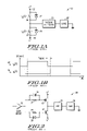
- FIG. 1A illustrates switching circuit 10 which is an example of a switching circuit commonly used in the art.
- a first terminal of switch 16 and a first terminal of diode 17 are coupled to V+ node 12
- a second terminal of switch 16 and a second terminal of diode 17 are coupled to passive LC filter 20 , a first terminal of switch 18 , and a first terminal of diode 19 .
- a second terminal of switch 18 and a second terminal of diode 19 are coupled to V ⁇ node 14 (where V ⁇ node 14 may be a ground node).
- Passive LC filter 20 is further coupled to a first terminal of load 22 , and the second terminal of load 22 is coupled to ground.
- Switches 16 and 18 are implemented with high power transistors.
- Input signal q p (t) 24 controls switch 16
- input signal q n (t) 26 controls switch 18
- Both signals 24 and 26 are square waves used to control the switches. However, since high power transistors are used as switches 16 and 18 , a significant portion of the time is spent in the switches' transitions. This leads to the problem that both switches 16 and 18 may either be open or closed at the same time. If they are both closed at the same time, a short circuit path from V+ to V ⁇ is created thereby causing excess power dissipation. If both switches 16 and 18 are open and diodes 17 and 19 are not present, passive LC filter 20 no longer receives a current path which causes a voltage stress and non-linearity in the circuit. Therefore, one prior art solution includes adding a dead time to signal 24 as shown in FIG. 1B . Alternatively, a dead time may be added to signal 26 .
- FIG. 1B illustrates a t dead delay time which prevents signals 24 and 26 from being on at the same time.
- this solution is undesirable because a current path must be created for the time t dead when both switches are off.
- This situation adds extra elements and signal lines to circuit 10 .
- These extra elements include diodes 17 and 19 which are placed in parallel with switches 16 and 18 , respectively, to provide the necessary current path.
- these diodes are non-linear elements which cause distortion and non-linearity in switching circuit 10 . Therefore, a need exists to find a solution for a switching circuit that removes these extra elements and provides a more linear circuit.
- two separate gate drivers are needed to drive switches 16 and 18 which adds more elements and inputs to the circuit, thereby increasing the cost.
- FIG. 2 illustrates another prior art solution to switching circuit 10 .
- FIG. 2 illustrates switching circuit 28 which uses only one gate driver 30 whose output is coupled to a first terminal of resister 32 , a first terminal of diode 36 , a first terminal of resistor 34 , and a first terminal of diode 38 .
- a second terminal of diode 36 and a second terminal of resistor 32 are coupled to the gate of a PMOS transistor 40 .
- a second terminal of resistor 34 and a second terminal of diode 38 are coupled to the gate of NMOS transistor 42 .
- the drain of PMOS transistor 40 is coupled to the drain of NMOS transistor 42 and coupled to a first terminal of low pass filter 44 .
- the source of PMOS transistor 40 is coupled to node V+, while the source of NMOS transistor 42 is coupled to node V ⁇ (where V ⁇ may be a ground node).
- a second terminal of low pass filter 44 is coupled to a first terminal of load 46 , and a second terminal of load 46 is coupled to ground.
- resistors 32 and 34 work with the gate-to-source capacitances of transistors 40 and 42 , respectively, to introduce a delay in the gate to source voltages.
- Diodes 36 and 38 guarantee that this delay is introduced in only one direction and not the other. This solution, therefore, provides the required dead time analogous to t dead of FIG. 1B .
- diodes 36 and 38 are non-linear elements which introduce non-linearity into circuit 28 , and the switching time of transistors 40 and 42 are slowed down thus introducing greater dissipation.
- sampling is used to generate signals used in switching circuits.
- the sampling process and the switching process introduce disturbances into applications, such as power generation, amplification and control, reducing the accuracy of the output signal.
- applications such as power generation, amplification and control, reducing the accuracy of the output signal.
- the power supply and nonlinearities in the switches introduce harmonic distortion, corrupting the output audio signal.
- FIG. 1A illustrates a switching circuit currently used in the art.
- FIG. 1B illustrates input signals used to control the switches of the switching circuit in FIG. 1A .
- FIG. 2 illustrates a second switching circuit currently used in the art.
- FIG. 3 illustrates a switching circuit in accordance with one embodiment of the present invention.
- FIG. 4 illustrates a push-pull switching circuit in accordance with one embodiment of the present invention.
- FIG. 5 illustrates a simplified version of the push-pull switching circuit of FIG. 4 in accordance with another embodiment of the present invention.
- FIG. 6 illustrates the use of a break-before-make element in combination with two switches in accordance with one embodiment of the present invention.
- FIG. 7 illustrates a passive break-before-make element in accordance with one embodiment of the present invention.
- FIG. 8 illustrates a passive break-before-make element in accordance with another embodiment of the present invention.
- FIG. 9 illustrates a make-before-break element used in combination with two switches in accordance with one embodiment of the present invention.
- FIG. 10 illustrates a make-before-break element in accordance with one embodiment of the present invention.
- FIG. 11 illustrates a circuit to provide analog feedback using a differential duty ratio adjuster in accordance with one embodiment of the present invention.
- FIG. 12A illustrates a circuit implementation of the duty ratio adjuster in accordance with one embodiment of the present invention.
- FIG. 12B illustrates a circuit implementation of the differential duty ratio adjuster in accordance with one embodiment of the present invention.
- FIG. 13 illustrates the waveform at the output of the duty ratio adjuster in accordance with one embodiment of the present invention.
- FIG. 14 illustrates a circuit implementation of the differential duty ratio adjuster suitable for implementation in an integrated circuit.
- passive elements refer to elements such as resistors, capacitors, and inductors. Switches are considered on when they are closed and form a connection, and they are considered off when they are open or break a connection.
- nodes V+ and V ⁇ refer to terminals where the voltage at V+ is greater than the voltage at V ⁇ . In some embodiments, node V ⁇ may be a ground node.
- FIG. 3 illustrates switching circuit 48 in accordance with one embodiment of the present invention.
- Node V+ 50 is coupled to a first terminal of switch 58 .
- a second terminal of switch 58 is coupled to a first terminal of break-before-make (BBM) element 54 , and the second terminal of BBM element 54 is coupled to the first terminal of BBM element 56 and a first terminal of low pass filter 61 .
- a second terminal of low pass filter 61 is coupled to a first terminal of load 62 , and a second terminal of load 62 is coupled to ground.
- the second terminal of BBM element 56 is coupled to a first terminal of switch 60 , and the second terminal of switch 60 is coupled to node V ⁇ 52 .
- BBM element 54 includes a resistor R p in parallel with an inductor L p
- BBM element 56 includes a resistor R n in parallel with inductor L n . Therefore, BBM elements 54 and 56 are considered passive BBM elements.
- switch 58 is a high power PMOS transistor
- switch 60 is a high power NMOS transistor.
- Input signals q p (t) and q n (t) are used to control switches 58 and 60 respectively.
- signals q p (t) and q n (t) may be the same signal out of a gate drive output. This allows for the use of a single gate driver for both switches 58 and 60 .
- BBM elements 54 and 56 work to limit the current through the short circuit path. Most of the time, current flows through either inductor L p or inductor L n depending upon which switch 58 or 60 is turned on.
- resistors R p and R n and inductors L p and L n are chosen such that a sufficient time constant of L/R is provided during the switching transitions.
- the values of R p , R n , L p , and L n are also chosen to minimize the switching stress on switches 58 and 60 .
- the resistors and inductors of BBM elements 54 and 56 are linear passive elements which do not introduce non-linearity during the switching transitions. Passive BBM elements 54 and 56 , by reducing non-linearity, reduce distortion caused by the switching transitions that is seen by low pass filter 61 and load 62 .
- These BBM elements 54 and 56 allow for reduced numbers of parts and components, reduced signal lines, reduced costs, and improved linearity.
- switching circuit 48 may be used for a digital audio amplifier wherein improved linearity is an important element.
- Alternate embodiments may include different elements within the passive BBM elements or may include only one BBM, as opposed to two as illustrated in FIG. 3 .
- the BBM elements discussed throughout herein are designed to have a relatively high impedance during short terms and low impedance during long terms. That is, the short terms refer to the switching transitions where the current changes rapidly, and the long terms refer to those times, other than the switching times, where the current remains fairly constant.
- these BBM elements reduce electromagnetic interference (EMI) by limiting the rate of change of the current taken from the power supply. Therefore, the EMI concerns of the switching circuit are reduced or eliminated.
- alternate embodiments may use PNP transistors in place of the PMOS transistors and NPN transistors in place of the NMOS transistors as the switches. Alternatively, other semiconductor switching elements may be used as the switches.
- FIG. 4 illustrates a push-pull system using passive BBM elements in accordance with one embodiment of the present invention.
- Push-pull switching circuit 64 includes four switches 70 , 72 , 88 , and 90 , and four BBM elements 74 , 76 , 92 , and 94 .
- Input signal S 1 66 is input to gate driver 68 whose output is coupled to switches 70 and 72 .
- the output of gate drive 68 is coupled to the gate of PMOS transistor 70 and the gate of NMOS transistor 72 .
- the source of PMOS transistor 70 is coupled to node V+ and the source of NMOS transistor 72 is coupled to node V ⁇ .
- the drain of PMOS transistor 70 is coupled to a first terminal of BBM element 74 , and the second terminal of BBM element 74 is coupled to a first terminal of low pass filter 78 and a first terminal of BBM element 76 .
- the second terminal of BBM element 76 is coupled to the drain of NMOS transistor 72 .
- Input signal S 1 — bar 98 is input to gate driver 96 whose output is coupled to switches 88 and 90 .
- the output of gate drive 96 is coupled to the gate of PMOS transistor 88 and the gate of NMOS transistor 90 .
- the source of PMOS transistor 88 is coupled to node V+ and the source of NMOS transistor 90 is coupled to the node V ⁇ .
- the drain of PMOS transistor 88 is coupled to a first terminal of BBM element 92
- the second terminal of BBM element 92 is coupled to a second terminal of low pass filter 78 and a first terminal of BBM element 94
- the second terminal of BBM element 94 is coupled to the drain of NMOS transistor 90 .
- Low pass filter 78 is coupled to load 86 .
- Low pass filter 78 includes inductor 80 , capacitor 84 , and inductor 82 .
- a first terminal of inductor 80 is coupled to the second terminal of break before make element 74 and the first terminal of break before make element 76 .
- the second terminal of inductor 80 is coupled to a first terminal of load 86 and a first terminal of capacitor 84 .
- the second terminal of capacitor 84 is coupled to a second terminal of load 86 and a first terminal of inductor 82 .
- the second terminal of inductor 82 is coupled to the second terminal of make before break element 92 and the first terminal of make before break element 94 .
- switching circuit 64 of FIG. 4 is a push-pull version of switching circuit 48 of FIG. 3 .
- the push-pull version 64 uses the symmetry between PMOS transistors 70 and 88 and NMOS transistors 72 and 90 to increase the linearity of the system.
- switching circuit 64 only one gate driver 68 is necessary to control both switches 70 and 72 , and only one gate driver 96 is required to control both switches 88 and 90 . This eliminates the need for a separate gate driver for each switch as used in the prior art (for example, see FIG. 1A ).
- switching circuit 64 may be used in a digital audio amplifier system.
- input signals S 1 66 and S 1 — bar 98 are received from a digital signal processor. Therefore, switching circuit 64 , by reducing the number of gate drivers and input signals required, reduces the number of pins needed on a digital signal processor.
- low pass filter 78 prefers to see a current path at all times; therefore, the resistors of the BBM elements provide a current path at all times including during the switch transitions.
- the values of the resistors and inductors of the BBM elements are chosen based upon the impedance of the load and the switching transition characteristics of transistors 70 , 72 , 88 , and 90 .
- the inductors of the BBM elements are chosen to be 43 nanohenries and the resistors of the BBM elements are chosen to be 10 ohms when the load is 8 ohms and the supply voltage is 20 volts.
- alternate embodiments may choose different values for the inductors and the resistors based upon different loads and supply voltages and different characteristics of transistors 70 , 72 , 88 , and 90 , and switching circuit 64 .
- switching circuit 64 may be designed without BBM elements 74 and 92 .
- switching element 64 may be designed without BBM elements 76 and 94 . In this manner, switching circuit 64 may include only two BBM elements rather than four. Also, alternate embodiments may place the BBM elements between the voltage nodes V+ or V ⁇ and the sources of the transistors.
- FIG. 5 illustrates an alternate embodiment of switching circuit 64 illustrated in FIG. 4 .
- FIG. 5 illustrates push-pull switching circuit 100 which includes switches 106 , 108 , 116 , and 118 , low pass filter 112 , and BBM element 110 .
- V+ node 102 is coupled to a first terminal of switch 106 and a first terminal of switch 116 .
- the second terminal of switch 106 is coupled to a first terminal of low pass filter 112 and a first terminal of switch 108 .
- the second terminal of switch 116 is coupled to a second terminal of low pass filter 112 and a first terminal of switch 118 .
- the second terminal of switch 108 and the second terminal of switch 118 is coupled to a first terminal of make before break element 110 , and the second terminal of make before break element is coupled to node V ⁇ 104 .
- Low pass filter 112 is coupled to load 114 .
- a signal S 1 119 is input to gate driver 120 whose output is coupled to switches 106 and 108 .
- Signal S 1 — bar 121 the inverse of signal S 1 119 , is input to gate drive 122 whose output is coupled to switches 116 and 118 .
- switches 106 and 116 may be high power PMOS transistors while switches 108 and 118 may be high power NMOS transistors wherein the output of drivers 120 and 122 are coupled to the gates of the transistors.
- push-pull switching circuit 100 of FIG. 5 is a modified version of switching circuit 64 of FIG. 4 that maintains the BBM action while using a reduced number of parts.
- the four BBM elements of FIG. 4 ( 74 , 76 , 92 , and 94 ) have been reduced into a single BBM element 110 .
- BBM element 110 may be placed between V+ node 102 and the first terminals of switches 106 and 116 rather than between node V ⁇ 104 and the second terminals of switches 108 and 118 .
- Single BBM element 110 is designed to provide the same advantages as the four BBM elements of FIG. 4 .
- resistor R n of BBM element 110 provides a current path at all times, including the switching transitions, to low pass filter 112 . Therefore, switching circuit 100 is a simplified circuit that maintains efficiency.
- FIG. 6 illustrates the basic structure of a switching circuit containing a BBM element in accordance with one embodiment of the present invention.
- Node V+ is connected to a first terminal of switch 132
- the second terminal of switch 132 is coupled to a first terminal of passive BBM element 136 .
- a second terminal of passive BBM element 136 is coupled to a first terminal of low pass filter 138 and a first terminal of switch 134 .
- the second terminal of switch 134 is coupled to ground, and a second terminal of low pass filter 138 is coupled to a first terminal of load 140 where a second terminal of load 140 is coupled to ground.
- BBM element 136 ensures that there is a current path available to low pass filter 138 at all times including during the switching times of switches 132 and 134 . Since BBM element 136 includes passive linear elements (i.e. resistors, inductors, and/or capacitors), BBM element 136 does not introduce any non-linearity during the switching transitions. Furthermore, BBM element 136 may be placed at any point between nodes V+ and V ⁇ . For example, BBM element 136 may be placed between the node V+ and the first terminal of switch 132 or between V ⁇ and the second terminal of switch 134 .
- FIG. 7 illustrates one embodiment of a BBM element in accordance with one embodiment of the present invention.
- BBM 142 may be used for BBM 136 in FIG. 6 .
- BBM element 142 is a passive BBM element that includes inductor 146 coupled in parallel with resistor 144 . In operation, during the transition times of the switches within a switching circuit, the current flows through resistor 144 . However, during the other times the current will flow through inductor 146 .
- BBM 142 is designed such that a high impedance exists for the short term (such as during the transitions) and a low impedance for the long term (such as the times surrounding the transitions).
- FIG. 8 illustrates a passive BBM element in accordance with an alternate embodiment of the present invention.
- Passive BBM element 148 may also be used in place of BBM 136 in FIG. 6 and includes inductor 154 coupled in parallel with resistor 150 that is in series with capacitor 152 .
- the presence of capacitor 152 reduces the dissipation during the transition times when current is flowing through resistor 150 and capacitor 152 .
- the LC time constant may be chosen to be resonant with the switching transition time. Therefore, the values of inductor 154 , resistor 150 , and-capacitor 152 are chosen to provide the proper time constant.
- BBM elements 142 of FIG. 7 and 148 of FIG. 8 both improve efficiency and linearity of switching circuits while reducing input lines, number of components, and dissipation.
- FIG. 9 illustrates a switching circuit utilizing a make-before-break (MBB) element in accordance with one embodiment of the present invention.
- Switching circuit 156 illustrates the mathematical converse or inverse of switching circuit 130 of FIG. 6 . In this transformation, for example, inductors become capacitors and connections in series become connections in parallel.
- Switching circuit 156 includes load 166 , low pass filter 164 , switches 158 and 160 , and MBB element 162 . Node V+ is connected to a first terminal of switch 158 , and the second terminal of switch 158 is coupled to a first terminal of low pass filter 164 , a first terminal of switch 160 , and a first terminal of MBB element 162 .
- the second terminal of switch 160 is coupled to node V ⁇ , and the second terminal of MBB element 162 is coupled to ground.
- a second terminal of low pass filter 164 is coupled to a first terminal of load 166 , and the second terminal of load 166 is coupled to ground.
- Switching circuit 156 is designed such that switches 158 and 160 will never be turned on simultaneously. However, they may be turned off simultaneously, thus creating an open circuit between V+ and V ⁇ .
- MBB element 162 provides a current path to low pass filter 164 . Therefore, MBB 162 ensures that low pass filter 164 will have a current path at all times, analogous to the function of the BBM elements described herein above.
- FIG. 10 illustrates a MBB element 168 in accordance with one embodiment of the present invention.
- this MBB may be used in switching circuit 156 of FIG. 9 .
- MBB element 168 includes resistor 170 coupled in series with capacitor 172 .
- capacitor 172 provides a current path to low pass filter 164 .
- the passive MBB elements described above provide similar advantages to the passive BBM elements described above.
- the MBB elements also provide a current path in the short term, reduce cost, improve efficiency, and reduce or eliminate EMI concerns.
- the above embodiments illustrate switching circuits using BBM and MBB elements that improve linearity, reduce the number of components and input signals required, reduce cost, and improve efficiency over known techniques.
- these switching circuits may be used in a digital audio application to provide the above advantages.
- the load may be a speaker, and the reduction in the number of input signals required may simplify connection of the switching circuit to a digital signal processor.
- the switching circuits described above may be composed of discrete components found on a circuit board or may be designed as integrated circuit chips.
- alternate embodiments may not include a low pass filter coupled between the switches and the load. That is, filter 61 of FIG. 3 , filter 78 of FIG. 4 , filter 112 of FIG.
- filter 138 of FIG. 6 may be removed from the circuits.
- other filters may be used.
- the loads for example, load 62 , load 86 , load 114 , load 140 , or load 166
- the loads may be any appropriate load, such as a speaker.
- Switching circuits are used in a variety of applications, including power, control and amplification applications.
- large audio waveforms are used to drive audio speakers.
- the audio wave form is generated by a digital PWM signal switching a high voltage power supply.
- Digital sampling is used to generate the PWM signal used for power switching, where a digital signal processor (DSP) is generally used to generate the PWM signal.
- DSP digital signal processor
- the digital PWM signal will have an accuracy defined to be 16–20 bits depending on the input source.
- the audio output waveform is affected by noise in the power supply and nonlinearities introduced at the power stage.
- the nonidealities may result from switch nonlinearities, break-before-make, make-before-break, or nonidealities of the power supply.
- the nonlinearities result in harmonic distortion.
- the harmonic distortion is typically in the range of about 60 dB total harmonic distortion (THD).
- PDM pulse density modulation
- Embodiments of the present invention provide small adjustments to the digital PWM signal, which correct for these various disturbances without requiring a resampling of the PWM signal.
- the output of the power stage is provided to an integral feedback circuit to suppress the switching frequency while providing sufficient gain within the pass band of the system to improve linearity.
- One embodiment of the present invention increased the quality of the output audio waveform to 70 dB.
- a typical digital audio amplification system receives a signal from a digital source, such as a compact disk (CD), which is provided to a conversion block.
- the digital source is typically encoded using pulse code modulation (PCM). It is desirable to convert the PCM signal to a PWM signal.
- PCM pulse code modulation
- the output of the PCM to PWM conversion is then provided to a Class-D amplifier.
- the output of the amplifier is then put through an LC low pass filter and provided to the load, which in this case is typically a speaker.
- a Class-D amplifier may be either half bridge or full bridge with switches driven either by the PWM signal, its compliment, or a modification thereof.
- these switches are power MOSFETS or BJT's. All of the typical switches are non-linear devices, introducing distortion into the audio information. Within such a system the first distortion is introduced during the PCM to PWM conversion, so the Class-D amplifier receives an already distorted signal.
- the switches are not ideal and large currents are typically involved in an amplification at this power stage, the output of the power stage includes various non-linerarities. Typical power stages also exhibit very low power supply rejection, meaning that any interference present on the supply rails during the amplification process will appear at the output as well.
- Other channels within the digital audio amplification system have an additional impact on such distortions.
- One solution to reducing cross talk between channels is the use of separate power supplies, however this is a costly solution.
- a method for correcting small non-linearities created in the power stage of an audio amplifier, introduced by the switching operation uses analog feedback to generate a power stage output waveform that is an accurate replica of the original input PWM signal, i.e. free from processing distortions.
- the analog feedback is used to modulate the duty ratio of the original input PWM signal.
- the method provides power supply noise rejection, which in turn reduces crosstalk between channels.
- each channel is a separate amplification path. For example, a first channel is a path to a first stereo speaker and a second channel is a path to a second speaker.
- a duty ratio modulator is used to adjust input PWM signals.
- PWM signal or “PWM input” will be used to refer to the signal being processed throughout a system.
- the PWM signal is defined by magnitude and duty ratio, which may change throughout processing due to various distortions introduced by the process.
- the edges of the pulses in the adjusted PWM signal are delayed with respect to the input PWM signal, and the duty ratio of the signal is adjusted with respect to the output voltage of the power stage.
- FIG. 11 One embodiment of a power stage having a switching circuit with feedback 200 is illustrated in FIG. 11 , where a Differential Duty Ratio Adjuster (DDRA) 202 receives a PWM input and a first control voltage, V 1 .
- the DDRA 202 has a first output corresponding to point B, which is provided to a power stage 204 .
- Power stage 204 is powered by large power supply, which is often used to power multiple amplifiers within a given system.
- the PWM signal of point B controls the switching of elements within the power stage 204 .
- the power stage amplifies the PWM signal, and provides an amplified PWM signal to a low pass filter (LPF) 210 and to a summing node 206 .
- LPF low pass filter
- the filtered output of LPF 210 is provided to load 212 .
- the DDRA 202 has a second output corresponding to point A, which is provided to a summing node 206 .
- the output of power stage 204 is subtracted from the output of node A. In this way, the output of the power stage is compared to a clean PWM signal, and the difference is used to generate integrated feedback.
- the resultant difference of summing node 206 is provided to an error amplifier 208 , where it is amplified such that it realizes a high gain at audio frequencies and a low gain at the switching frequency.
- the error amplifier 208 includes an integrator to generate an amplified error signal, voltage V f that is provided to DDRA 202 .
- the amplified error signal provides feedback information to the DDRA 202 which is used to adjust the duty ratio of the PWM signal.
- error amplifier 208 generates (V f ) and its compliment ( ⁇ V f ), where both are provided as feedback to DDRA 202 .
- DDRA 202 adjusts the duty ratio of the PWM input signal, and balances the delay between the two paths going to summing node 206 .
- DDRA 202 provides the PWM input signal to a digital gate 224 , the output of which is provided to digital gate 222 and to duty ratio modulator 230 .
- the digital gate 224 reduces extraneous noise in the PWM input.
- the digital gate 224 acts as a digital receiver and repeats the high and low signals without the noise.
- Duty ratio modulator 230 receives the error amplifier signal V f from error amplifier 208 , as illustrated FIG. 11 .
- the output of the duty ratio modulator 230 is then provided to a digital gate 232 .
- a control voltage, V 1 controls the amount of delay for the digital gate 232 .
- the output of digital gate 232 is then provided to power stage 204 .
- duty ratio modulator 230 introduces a delay into the PWM signal, the upper path illustrated in FIG. 12A compensates for that delay.
- the digital gate 222 introduces a compensatory delay prior to summing node 206 .
- Digital gate 222 also receives a consistent control voltage, V 1 .
- V 1 a low noise power supply generates V 1 throughout switching circuit 200 .
- the control voltage, V 1 is provided by a separate power supply from that supplying the power stage 204 .
- the digital ratio modulator 230 replicates the original input PWM signal which has been distorted by digital processing. Within duty ratio modulator 230 , the PWM signal is initially smoothed by resistor R 1 and capacitor C, where the output edge transitions are slowed. The result is a replica of the original undistorted PWM input with extended rise times and fall times.
- Digital gate 232 functions as a comparator having a fixed threshold voltage, V T .
- the output of digital gate 232 is illustrated in FIG. 13 , where D corresponds to the duty ratio of the power stage, and T corresponds to the period.
- the duty ratio at the output of digital gate 232 is given as DT/T, which is equal to D. This is provided as input to power stage 204 .
- the rising and falling edges of the resultant signal are delayed and sloped.
- the magnitude of the signal may increase or decrease with respect to V T .
- the amplified error signals V f and its complement ( ⁇ V f ) are used to shift the signal up and down, effectively self-correcting the duty ratio D based on the output of the power stage 204 .
- the error signal provided to error amplifier 208 will decrease.
- a reduced error signal input to error amplifier 208 results in a reduced amplified error output.
- a corresponding reduction in the entire signal is seen at point C of FIG. 12A , where the duty ratio, D, will decrease slightly.
- the output of power stage 204 will return to a correct value.
- Embodiments of the present invention provide a high power supply rejection (PSRR) that reduces the crosstalk between channels within an amplification system.
- Error amplifier 208 is designed such that the integrator behavior acts as a low pass filter having a bandwidth sufficient for an audio band but which rejects the switching frequency.
- FIG. 12B An alternate embodiment of the present invention is illustrated in FIG. 12B , where the DDRA 203 is similar to the DDRA 202 of FIG. 12A with an additional second duty ratio modulator 220 coupled between digital gate 224 and digital gate 222 .
- digital gate 222 and digital gate 232 both receive voltage V 1 .
- the duty ratio modulator 220 is added to compensate for delays introduced by duty ratio modulator 230 .
- duty ratio modulator 230 introduces a delay in the PWM signal in the path of node B, it is duplicated in the reference path of node A to repeat the same delay.
- Feedback information is provided to duty ratio modulator 230 by V f , while its complement, ( ⁇ V f ) is provided to duty ratio modulator 220 .
- the amplified error signals adjust the duty ratio of the PWM signal, where V f and ( ⁇ V f ) have opposite effects on the duty ratio of the PWM signal, reducing the difference seen at summing node 206 .
- Each of the modulators 220 and 230 include RC circuit elements which introduce a same delay into each path. In this way the delay between the two signals received at summing node 206 is minimized.
- FIG. 13 illustrates the voltage seen at capacitor C within duty ratio modulator 230 .
- time is represented on the horizontal axis
- voltage V C is represented on the vertical axis.
- the threshold voltage V T is given as a fixed voltage level. T corresponds to the period of the signal, and the pulse width of the signal is defined as the product of the duty ratio, D, and the period, T. As illustrated both the rising edge and the falling edges are sloped.
- V f tends to raise the entire V C signal.
- V C decreases with decreasing V f .
- FIG. 14 An alternate embodiment of DDRA 202 , as illustrated in FIG. 11 , is provided in FIG. 14 .
- DDRA 240 receives a PWM input signal and channels it to two paths.
- a first path provides the PWM signal to block 252 to generate the clean PWM signal, while a second path provides the PWM signal to block 242 for duty ration adjustment.
- the output of block 242 corresponds to point A as indicated in FIG. 11 .
- the output of block 252 corresponds to point B as indicated in FIG. 11 .
- Block 242 includes two parallel delay lines comprising of logic gates circuits 244 and 246 .
- the PWM signal is an input to circuit 244
- the inverted PWM is an input to circuit 246 .
- Circuit 244 provides an S input to latch 248
- integration circuit 246 provides an R input to latch 248 .
- S and R represent set and reset respectively.
- the latch 248 is not clocked.
- the output transitions are governed entirely by the inputs S and R.
- Delay circuit 244 receives control voltage signal V 1 , where two integrators are coupled in tandem.
- Delay circuit 246 is configured to have an additional inversion at its input since it feeds the reset node of the S-R latch.
- Block 252 is similar to block 242 , having delay circuits 254 and 256 , each providing input signals S and R, respectively, to latch 258 .
- Circuit 254 receives the PWM signal, while circuit 256 receives the inverted PWM signal.
- the latch 258 is not clocked. It toggles according to the inputs S and R.
- integration circuit 254 receives the sum of V 1 plus V f .
- Integration circuit 256 receives the difference of V 1 and V f .
- the control voltage V 1 is typically a fixed voltage, while the error voltage V f is variable.
- block 252 tends to increase the duty ratio of the output pulse when V f increases and reduces the length of the output pulse as V f decreases.
- V 1 is basically a fixed value, the increase is due to increased V f .
- the effect on block 256 of increased V f produces a longer delay at the R input to latch 258 , i.e. the signal falling edge appears more quickly.
- the rising edge of a pulse will have only a slight delay while the falling edge will have a much larger delay. This increases the length of the pulse.
- latch 258 is set with a greater delay and reset with less delay. In this case the pulse length is shortened as the rising edge is delayed while the falling edge occurs more quickly. As illustrated in FIG. 14 , small changes in the output voltage V f may have the desired impact on the duty ratio of the adjusted PWM signal.
- Embodiments of the present invention also provide a method for correction of nonlinearities using analog feedback from a switching circuit, where the switching circuit starts with a digitally generated switching signal.
- a correction circuit corrects for switch nonlinearities, nonlinearities due to break before make as well as nonidealities of the power supply.
- the analog feedback circuit achieves improved linearity, rejects power supply noise and reduces crosstalk between multiple channels operating from the same power supply.
- the correction works by modifying in analog domain the duty ratio of the digitally generated switching signal.
- the correction circuit can be implemented with discrete components or inside an integrated circuit.
- a switching circuit having feedback includes a differential duty ratio adjuster (DDRA) having a first input to receive a pulse width modulation (PWM) signal, a second input to receive a reference voltage, and a third input to receive a first feedback signal.
- the DDRA includes a first digital gate having a first input to receive the PWM signal, a first duty ratio modulator having a first input to receive the PWM signal and a second input to receive the first feedback signal, and a second digital gate having a first input to receive an output of the first duty ratio modulator.
- a method of providing feedback to a switching circuit includes a power stage.
- the method includes receiving a PWM signal, adjusting the PWM signal to form a lower noise PWM signal, modulating the PWM signal using feedback to form a corrected PWM signal, providing the corrected PWM signal to the power stage to produce an amplified PWM signal, and producing a feedback signal based at least in part on the amplified PWM signal and the lower noise PWM signal.
Abstract
Description
Claims (29)
Priority Applications (1)
| Application Number | Priority Date | Filing Date | Title |
|---|---|---|---|
| US10/828,090 US6995482B2 (en) | 2000-01-05 | 2004-04-20 | Switching circuit and method therefor |
Applications Claiming Priority (2)
| Application Number | Priority Date | Filing Date | Title |
|---|---|---|---|
| US47798500A | 2000-01-05 | 2000-01-05 | |
| US10/828,090 US6995482B2 (en) | 2000-01-05 | 2004-04-20 | Switching circuit and method therefor |
Related Parent Applications (1)
| Application Number | Title | Priority Date | Filing Date |
|---|---|---|---|
| US47798500A Division | 2000-01-05 | 2000-01-05 |
Publications (2)
| Publication Number | Publication Date |
|---|---|
| US20040195918A1 US20040195918A1 (en) | 2004-10-07 |
| US6995482B2 true US6995482B2 (en) | 2006-02-07 |
Family
ID=33098343
Family Applications (1)
| Application Number | Title | Priority Date | Filing Date |
|---|---|---|---|
| US10/828,090 Expired - Fee Related US6995482B2 (en) | 2000-01-05 | 2004-04-20 | Switching circuit and method therefor |
Country Status (1)
| Country | Link |
|---|---|
| US (1) | US6995482B2 (en) |
Cited By (2)
| Publication number | Priority date | Publication date | Assignee | Title |
|---|---|---|---|---|
| US20080150484A1 (en) * | 2006-12-22 | 2008-06-26 | Kimball Jonathan W | Modular System for Unattended Energy Generation and Storage |
| US20090107149A1 (en) * | 2007-10-25 | 2009-04-30 | Honeywell International Inc. | Current-protected driver circuit for ignition exciter unit |
Families Citing this family (2)
| Publication number | Priority date | Publication date | Assignee | Title |
|---|---|---|---|---|
| EP1592032A1 (en) * | 2004-04-30 | 2005-11-02 | Alcatel | Mechanical switching circuit |
| CA2675303A1 (en) * | 2007-01-25 | 2008-07-31 | Rgb Systems, Inc. | Method and apparatus for producing triangular waveform with low audio band noise content |
Citations (6)
| Publication number | Priority date | Publication date | Assignee | Title |
|---|---|---|---|---|
| WO1998044626A2 (en) | 1997-04-02 | 1998-10-08 | Karsten Nielsen | Pulse referenced control method for enhanced power amplification of a pulse modulated signal |
| US5933453A (en) * | 1997-04-29 | 1999-08-03 | Hewlett-Packard Company | Delta-sigma pulse width modulator control circuit |
| WO1999059241A2 (en) | 1998-05-11 | 1999-11-18 | Toccata Technology Aps | A method of reducing distortion and noise of square-wave pulses, a circuit for generating minimally distorted pulses and use of method and circuit |
| US6414613B1 (en) | 2000-01-05 | 2002-07-02 | Motorola, Inc. | Apparatus for noise shaping a pulse width modulation (PWM) signal and method therefor |
| US6473457B1 (en) | 1999-05-07 | 2002-10-29 | Motorola, Inc. | Method and apparatus for producing a pulse width modulated signal |
| US6665338B1 (en) | 2000-01-05 | 2003-12-16 | Motorola, Inc. | Circuitry for converting a sampled digital signal to a naturally sampled digital signal and method therefor |
-
2004
- 2004-04-20 US US10/828,090 patent/US6995482B2/en not_active Expired - Fee Related
Patent Citations (6)
| Publication number | Priority date | Publication date | Assignee | Title |
|---|---|---|---|---|
| WO1998044626A2 (en) | 1997-04-02 | 1998-10-08 | Karsten Nielsen | Pulse referenced control method for enhanced power amplification of a pulse modulated signal |
| US5933453A (en) * | 1997-04-29 | 1999-08-03 | Hewlett-Packard Company | Delta-sigma pulse width modulator control circuit |
| WO1999059241A2 (en) | 1998-05-11 | 1999-11-18 | Toccata Technology Aps | A method of reducing distortion and noise of square-wave pulses, a circuit for generating minimally distorted pulses and use of method and circuit |
| US6473457B1 (en) | 1999-05-07 | 2002-10-29 | Motorola, Inc. | Method and apparatus for producing a pulse width modulated signal |
| US6414613B1 (en) | 2000-01-05 | 2002-07-02 | Motorola, Inc. | Apparatus for noise shaping a pulse width modulation (PWM) signal and method therefor |
| US6665338B1 (en) | 2000-01-05 | 2003-12-16 | Motorola, Inc. | Circuitry for converting a sampled digital signal to a naturally sampled digital signal and method therefor |
Non-Patent Citations (4)
| Title |
|---|
| Kimball, J. et al; "Continuous-time optimization of gate timing for synchronous rectification"; IEEE 39<SUP>th </SUP>Midwest Symposium on Circuits and Systems; Aug. 18-21, 1996; pp 1015-1018; vol. 3; IEEE. |
| Midya, P. et al.; "Sensorless current mode control-an observer-based technique for DC-DC converters"; Power Electronics Specialists Conference, Jun. 22-27, 1997; pp 197-202; vol. 1; IEEE. |
| Mosely, I.D. et al; "Effect of dead time on harmonic distortion in class-D audio power amplifiers"; Electronic Letters; Jun. 10, 1999; pp 920-952; vol. 35, Issue 12; IEEE. |
| Nielsen, Karsten; "PEDEC-A Novel Pulse Referenced Control Method for High Quality Digital PWM Switching Power Amplification"; IEEE; 1998; pp 200-207; IEEE. |
Cited By (4)
| Publication number | Priority date | Publication date | Assignee | Title |
|---|---|---|---|---|
| US20080150484A1 (en) * | 2006-12-22 | 2008-06-26 | Kimball Jonathan W | Modular System for Unattended Energy Generation and Storage |
| US7994657B2 (en) | 2006-12-22 | 2011-08-09 | Solarbridge Technologies, Inc. | Modular system for unattended energy generation and storage |
| US20090107149A1 (en) * | 2007-10-25 | 2009-04-30 | Honeywell International Inc. | Current-protected driver circuit for ignition exciter unit |
| US8027142B2 (en) | 2007-10-25 | 2011-09-27 | Honeywell International Inc. | Current-protected driver circuit for ignition exciter unit |
Also Published As
| Publication number | Publication date |
|---|---|
| US20040195918A1 (en) | 2004-10-07 |
Similar Documents
| Publication | Publication Date | Title |
|---|---|---|
| US7262658B2 (en) | Class-D amplifier system | |
| US6707337B2 (en) | Self-operating PWM amplifier | |
| JP6474697B2 (en) | Switching power amplifier | |
| US8189817B2 (en) | System for amplifiers with low distortion and low output impedance | |
| EP1042865B1 (en) | Pulse referenced control method for enhanced power amplification of a pulse modulated signal | |
| EP1183776B1 (en) | Power modulation systems and methods that separately amplify low and high frequency portions of an amplitude waveform | |
| US7843260B2 (en) | Method and apparatus for high performance class D audio amplifiers | |
| US7468632B2 (en) | Power supply rejection for pulse width modulated amplifiers and automatic gain control | |
| US6605991B2 (en) | Circuitry for creating a spectral null in a differential output switching amplifier and method therefor | |
| US8433028B2 (en) | Latency locked loop circuit for driving a buffer circuit | |
| Jiang | Fundamentals of audio class D amplifier design: A review of schemes and architectures | |
| US7683708B2 (en) | Digital amplifier with analogue error correction circuit | |
| KR20090091826A (en) | Error correction system for a class-d power stage | |
| US10389312B2 (en) | Bias modulation active linearization for broadband amplifiers | |
| US7061313B2 (en) | Dual feedback linear amplifier | |
| US20190348955A1 (en) | Bias modulation active linearization for broadband amplifiers | |
| US6995482B2 (en) | Switching circuit and method therefor | |
| US20210391856A1 (en) | Modulator circuit, corresponding device and method | |
| KR20040001734A (en) | D grade power amp preventing distortion of out waveform | |
| WO2017212676A1 (en) | Digital amplifier and output device | |
| TW202315306A (en) | Class-d amplifier with deadtime distortion compensation | |
| CN115811281A (en) | Linear amplifier and power supply modulator | |
| CN116073921A (en) | Circuit for correcting duty cycle and phase error of low additive noise differential signal | |
| KR20230131762A (en) | Audio system, class-d driver circuit and control method thereof | |
| Balmelli et al. | Linearization of class D amplifiers |
Legal Events
| Date | Code | Title | Description |
|---|---|---|---|
| AS | Assignment |
Owner name: CITIBANK, N.A. AS COLLATERAL AGENT, NEW YORK Free format text: SECURITY AGREEMENT;ASSIGNORS:FREESCALE SEMICONDUCTOR, INC.;FREESCALE ACQUISITION CORPORATION;FREESCALE ACQUISITION HOLDINGS CORP.;AND OTHERS;REEL/FRAME:018855/0129 Effective date: 20061201 Owner name: CITIBANK, N.A. AS COLLATERAL AGENT,NEW YORK Free format text: SECURITY AGREEMENT;ASSIGNORS:FREESCALE SEMICONDUCTOR, INC.;FREESCALE ACQUISITION CORPORATION;FREESCALE ACQUISITION HOLDINGS CORP.;AND OTHERS;REEL/FRAME:018855/0129 Effective date: 20061201 |
|
| CC | Certificate of correction | ||
| FPAY | Fee payment |
Year of fee payment: 4 |
|
| AS | Assignment |
Owner name: CITIBANK, N.A., AS COLLATERAL AGENT,NEW YORK Free format text: SECURITY AGREEMENT;ASSIGNOR:FREESCALE SEMICONDUCTOR, INC.;REEL/FRAME:024397/0001 Effective date: 20100413 Owner name: CITIBANK, N.A., AS COLLATERAL AGENT, NEW YORK Free format text: SECURITY AGREEMENT;ASSIGNOR:FREESCALE SEMICONDUCTOR, INC.;REEL/FRAME:024397/0001 Effective date: 20100413 |
|
| FPAY | Fee payment |
Year of fee payment: 8 |
|
| AS | Assignment |
Owner name: CITIBANK, N.A., AS NOTES COLLATERAL AGENT, NEW YOR Free format text: SECURITY AGREEMENT;ASSIGNOR:FREESCALE SEMICONDUCTOR, INC.;REEL/FRAME:030633/0424 Effective date: 20130521 |
|
| AS | Assignment |
Owner name: CITIBANK, N.A., AS NOTES COLLATERAL AGENT, NEW YOR Free format text: SECURITY AGREEMENT;ASSIGNOR:FREESCALE SEMICONDUCTOR, INC.;REEL/FRAME:031591/0266 Effective date: 20131101 |
|
| AS | Assignment |
Owner name: FREESCALE SEMICONDUCTOR, INC., TEXAS Free format text: PATENT RELEASE;ASSIGNOR:CITIBANK, N.A., AS COLLATERAL AGENT;REEL/FRAME:037354/0225 Effective date: 20151207 Owner name: FREESCALE SEMICONDUCTOR, INC., TEXAS Free format text: PATENT RELEASE;ASSIGNOR:CITIBANK, N.A., AS COLLATERAL AGENT;REEL/FRAME:037356/0553 Effective date: 20151207 Owner name: FREESCALE SEMICONDUCTOR, INC., TEXAS Free format text: PATENT RELEASE;ASSIGNOR:CITIBANK, N.A., AS COLLATERAL AGENT;REEL/FRAME:037356/0143 Effective date: 20151207 |
|
| AS | Assignment |
Owner name: MORGAN STANLEY SENIOR FUNDING, INC., MARYLAND Free format text: ASSIGNMENT AND ASSUMPTION OF SECURITY INTEREST IN PATENTS;ASSIGNOR:CITIBANK, N.A.;REEL/FRAME:037486/0517 Effective date: 20151207 |
|
| AS | Assignment |
Owner name: MORGAN STANLEY SENIOR FUNDING, INC., MARYLAND Free format text: ASSIGNMENT AND ASSUMPTION OF SECURITY INTEREST IN PATENTS;ASSIGNOR:CITIBANK, N.A.;REEL/FRAME:037518/0292 Effective date: 20151207 |
|
| AS | Assignment |
Owner name: NORTH STAR INNOVATIONS INC., CALIFORNIA Free format text: ASSIGNMENT OF ASSIGNORS INTEREST;ASSIGNOR:FREESCALE SEMICONDUCTOR, INC.;REEL/FRAME:037694/0264 Effective date: 20151002 |
|
| AS | Assignment |
Owner name: NXP, B.V., F/K/A FREESCALE SEMICONDUCTOR, INC., NETHERLANDS Free format text: RELEASE BY SECURED PARTY;ASSIGNOR:MORGAN STANLEY SENIOR FUNDING, INC.;REEL/FRAME:040925/0001 Effective date: 20160912 Owner name: NXP, B.V., F/K/A FREESCALE SEMICONDUCTOR, INC., NE Free format text: RELEASE BY SECURED PARTY;ASSIGNOR:MORGAN STANLEY SENIOR FUNDING, INC.;REEL/FRAME:040925/0001 Effective date: 20160912 |
|
| AS | Assignment |
Owner name: NXP B.V., NETHERLANDS Free format text: RELEASE BY SECURED PARTY;ASSIGNOR:MORGAN STANLEY SENIOR FUNDING, INC.;REEL/FRAME:040928/0001 Effective date: 20160622 |
|
| AS | Assignment |
Owner name: MORGAN STANLEY SENIOR FUNDING, INC., MARYLAND Free format text: CORRECTIVE ASSIGNMENT TO CORRECT THE REMOVE PATENTS 8108266 AND 8062324 AND REPLACE THEM WITH 6108266 AND 8060324 PREVIOUSLY RECORDED ON REEL 037518 FRAME 0292. ASSIGNOR(S) HEREBY CONFIRMS THE ASSIGNMENT AND ASSUMPTION OF SECURITY INTEREST IN PATENTS;ASSIGNOR:CITIBANK, N.A.;REEL/FRAME:041703/0536 Effective date: 20151207 |
|
| FEPP | Fee payment procedure |
Free format text: MAINTENANCE FEE REMINDER MAILED (ORIGINAL EVENT CODE: REM.) |
|
| LAPS | Lapse for failure to pay maintenance fees |
Free format text: PATENT EXPIRED FOR FAILURE TO PAY MAINTENANCE FEES (ORIGINAL EVENT CODE: EXP.) |
|
| STCH | Information on status: patent discontinuation |
Free format text: PATENT EXPIRED DUE TO NONPAYMENT OF MAINTENANCE FEES UNDER 37 CFR 1.362 |
|
| FP | Expired due to failure to pay maintenance fee |
Effective date: 20180207 |
|
| AS | Assignment |
Owner name: SHENZHEN XINGUODU TECHNOLOGY CO., LTD., CHINA Free format text: CORRECTIVE ASSIGNMENT TO CORRECT THE TO CORRECT THE APPLICATION NO. FROM 13,883,290 TO 13,833,290 PREVIOUSLY RECORDED ON REEL 041703 FRAME 0536. ASSIGNOR(S) HEREBY CONFIRMS THE THE ASSIGNMENT AND ASSUMPTION OF SECURITYINTEREST IN PATENTS.;ASSIGNOR:MORGAN STANLEY SENIOR FUNDING, INC.;REEL/FRAME:048734/0001 Effective date: 20190217 |
|
| AS | Assignment |
Owner name: MORGAN STANLEY SENIOR FUNDING, INC., MARYLAND Free format text: CORRECTIVE ASSIGNMENT TO CORRECT THE REMOVE APPLICATION11759915 AND REPLACE IT WITH APPLICATION 11759935 PREVIOUSLY RECORDED ON REEL 037486 FRAME 0517. ASSIGNOR(S) HEREBY CONFIRMS THE ASSIGNMENT AND ASSUMPTION OF SECURITYINTEREST IN PATENTS;ASSIGNOR:CITIBANK, N.A.;REEL/FRAME:053547/0421 Effective date: 20151207 |
|
| AS | Assignment |
Owner name: NXP B.V., NETHERLANDS Free format text: CORRECTIVE ASSIGNMENT TO CORRECT THE REMOVEAPPLICATION 11759915 AND REPLACE IT WITH APPLICATION11759935 PREVIOUSLY RECORDED ON REEL 040928 FRAME 0001. ASSIGNOR(S) HEREBY CONFIRMS THE RELEASE OF SECURITYINTEREST;ASSIGNOR:MORGAN STANLEY SENIOR FUNDING, INC.;REEL/FRAME:052915/0001 Effective date: 20160622 |
|
| AS | Assignment |
Owner name: NXP, B.V. F/K/A FREESCALE SEMICONDUCTOR, INC., NETHERLANDS Free format text: CORRECTIVE ASSIGNMENT TO CORRECT THE REMOVEAPPLICATION 11759915 AND REPLACE IT WITH APPLICATION11759935 PREVIOUSLY RECORDED ON REEL 040925 FRAME 0001. ASSIGNOR(S) HEREBY CONFIRMS THE RELEASE OF SECURITYINTEREST;ASSIGNOR:MORGAN STANLEY SENIOR FUNDING, INC.;REEL/FRAME:052917/0001 Effective date: 20160912 |