US6996157B2 - Pattern generation circuit, multi-path detection circuit employing the same and multi-path detection method - Google Patents
Pattern generation circuit, multi-path detection circuit employing the same and multi-path detection method Download PDFInfo
- Publication number
- US6996157B2 US6996157B2 US09/770,506 US77050601A US6996157B2 US 6996157 B2 US6996157 B2 US 6996157B2 US 77050601 A US77050601 A US 77050601A US 6996157 B2 US6996157 B2 US 6996157B2
- Authority
- US
- United States
- Prior art keywords
- peak
- correlated
- delay profile
- path
- pattern
- Prior art date
- Legal status (The legal status is an assumption and is not a legal conclusion. Google has not performed a legal analysis and makes no representation as to the accuracy of the status listed.)
- Expired - Fee Related, expires
Links
- 238000001514 detection method Methods 0.000 title claims abstract description 103
- 230000002596 correlated effect Effects 0.000 claims abstract description 158
- 230000005540 biological transmission Effects 0.000 claims description 26
- 238000010276 construction Methods 0.000 description 19
- 238000010586 diagram Methods 0.000 description 12
- 238000000034 method Methods 0.000 description 12
- 230000002194 synthesizing effect Effects 0.000 description 3
- 238000006243 chemical reaction Methods 0.000 description 2
- 238000007796 conventional method Methods 0.000 description 2
- 230000000875 corresponding effect Effects 0.000 description 2
- 238000011112 process operation Methods 0.000 description 2
- 238000007792 addition Methods 0.000 description 1
- 230000000694 effects Effects 0.000 description 1
- 238000002474 experimental method Methods 0.000 description 1
- 238000001228 spectrum Methods 0.000 description 1
Images


Classifications
-
- H—ELECTRICITY
- H04—ELECTRIC COMMUNICATION TECHNIQUE
- H04B—TRANSMISSION
- H04B1/00—Details of transmission systems, not covered by a single one of groups H04B3/00 - H04B13/00; Details of transmission systems not characterised by the medium used for transmission
- H04B1/69—Spread spectrum techniques
- H04B1/707—Spread spectrum techniques using direct sequence modulation
- H04B1/7097—Interference-related aspects
- H04B1/711—Interference-related aspects the interference being multi-path interference
- H04B1/7113—Determination of path profile
-
- H—ELECTRICITY
- H04—ELECTRIC COMMUNICATION TECHNIQUE
- H04L—TRANSMISSION OF DIGITAL INFORMATION, e.g. TELEGRAPHIC COMMUNICATION
- H04L27/00—Modulated-carrier systems
- H04L27/18—Phase-modulated carrier systems, i.e. using phase-shift keying
- H04L27/22—Demodulator circuits; Receiver circuits
-
- H—ELECTRICITY
- H04—ELECTRIC COMMUNICATION TECHNIQUE
- H04B—TRANSMISSION
- H04B1/00—Details of transmission systems, not covered by a single one of groups H04B3/00 - H04B13/00; Details of transmission systems not characterised by the medium used for transmission
- H04B1/69—Spread spectrum techniques
- H04B1/707—Spread spectrum techniques using direct sequence modulation
- H04B1/709—Correlator structure
-
- H—ELECTRICITY
- H04—ELECTRIC COMMUNICATION TECHNIQUE
- H04B—TRANSMISSION
- H04B1/00—Details of transmission systems, not covered by a single one of groups H04B3/00 - H04B13/00; Details of transmission systems not characterised by the medium used for transmission
- H04B1/69—Spread spectrum techniques
- H04B1/707—Spread spectrum techniques using direct sequence modulation
- H04B1/7097—Interference-related aspects
- H04B1/711—Interference-related aspects the interference being multi-path interference
- H04B1/7115—Constructive combining of multi-path signals, i.e. RAKE receivers
- H04B1/7117—Selection, re-selection, allocation or re-allocation of paths to fingers, e.g. timing offset control of allocated fingers
Definitions
- the present invention relates to a pattern generation circuit, a multi-path detection circuit employing the same and a multi-path detection method. More particularly, the invention relates to a detection method of a multi-path position for determining a reception timing of a finger of a RAKE receiver employed in a code division multiple access (CDMA) system (spread spectrum system).
- CDMA code division multiple access
- a path timing detection circuit of this kind there is a circuit to be realized by measuring a delay profile of a propagation path by correlating operation of a reception signal and a spread code using a sliding correlator or matched filter and by detecting a correlation peak amount of the delay profile.
- a shape of the path has a width as illustrated in FIG. 5A .
- paths have enough interval as shown in FIG. 5B , a plurality of paths can be identified.
- the detected path position may be determined depending upon the set value to cause difficulty in detecting accurate timing.
- the present invention has been worked out in view of the problems set forth above. It is therefore an object of the present invention to provide a pattern generation circuit which can enhance precision in detection of each path timing and thus can obtain more stable reception performance, a multi-path detection circuit and a multi-path detection method employing the same.
- a pattern generating circuit comprises:
- generating means for generating a logical pattern of correlated peak in a delay profile of a transmission path
- removing means for removing a power component of the detected correlated peak from the delay profile using the logical pattern of the correlated peak generated by the generating means.
- a multi-path detection circuit for detecting a timing of multi-path by measuring a delay profile of a transmission path, comprises
- generating means for generating a logic pattern of a correlated peak in the delay profile
- detection means for detecting position of the correlated peak on the basis of the logical pattern of the correlated peak generated by the generating means.
- a multi-path detection circuit comprises:
- a matched filter outputting a correlated value of a spread code and a received signal
- delay profile storing means for storing a delay profile of a transmission path measured by the matched filter
- maximum value retrieving means for retrieving a maximum peak position and a peak level from the delay profile stored in the delay profile storing means
- pattern generating means for sequentially generating logical patterns of correlated peaks on the basis of the leak level and peak position obtained from the maximum value retrieving means;
- the maximum peak value and the peak level being retrieve sequentially from the profile generated by the generating means.
- a multi-path detection method for detecting a timing of multi-path by measuring a delay profile of a transmission path comprises the steps of:
- the multi-path detection circuit according to the present invention is to improve path detection accuracy in the environment where the path is located close in the extent of one chip in the multi-path detection circuit of CDMA type receiver unit.
- a multi-path detection circuit has generating means for generating a logic pattern of a correlated peak in the delay profile, and removing means for removing a power component of the detected correlated peak from the delay profile using the logical pattern of the correlated peak generated by the generating means.
- the multi-path detection circuit has a matched filter outputting a correlated value of a spread code and a received signal, delay profile storing means for storing a delay profile of a transmission path measured by the matched filter, maximum value retrieving means for retrieving a maximum peak position and a peak level of the first correlated peak from the delay profile stored in the delay profile storing means, pattern generating means for generating logical patterns (logical shape) of the first correlated peak on the basis of the leak level and peak position of the first correlated peak obtained from the maximum value retrieving means, and a substractor substracts the logical pattern of the first correlated peak from the delay profile data stored in the delay profile storage portion upon detecting the second correlated peak.
- delay profile storing means for storing a delay profile of a transmission path measured by the matched filter
- maximum value retrieving means for retrieving a maximum peak position and a peak level of the first correlated peak from the delay profile stored in the delay profile storing means
- pattern generating means for generating logical patterns (
- a profile removed the correlated power of the first correlated peak is prepared by the substractor upon detecting the second correlated peak to store in the delay profile storage portion.
- the maximum value retrieving portion outputs the maximum peak position and the peak level to obtain the peak level and the peak position of the second correlated peak.
- the pattern generating portion generates the logical pattern of the second correlated peak on the basis of the peak level and the peak position of the second correlated peak.
- the substractor subtracts the logical pattern of the second correlated peak from the delay profile data stored in the delay profile storage portion to generate a profile removed the correlated power of the second correlated peak to store.
- the foregoing operation is counted by the counter to repeat for a predetermined number to retrieve a plurality of correlated peak.
- the multi-path can be precisely separated into each individual path to enable detection of the correlated peak position to improve reception performance.
- FIG. 1 is a block diagram showing a construction of one embodiment of a multi-path detection circuit according the present invention
- FIG. 2 is a block diagram showing a construction of one embodiment of a CDMA receiver unit according to the present invention
- FIG. 3 is a block diagram showing an example of a construction of a maximum value retrieving portion of FIG. 1 ;
- FIG. 4 is a block diagram showing an example of a pattern generating portion of FIG. 1 ;
- FIG. 5A is an illustration showing a delay profile in case of one path
- FIG. 5B is an illustration of a delay profile in the case where intervals of three paths are relatively wide
- FIG. 5C is an illustration of a delay profile in the case where intervals of three paths are narrow.
- FIG. 6 is a flow chart showing an operation of the multi-path detection circuit of FIG. 1 ;
- FIGS. 7A to 7C are operation image of respective process for the delay profile data stored in a delay profile storage portion of FIG. 1 ;
- FIG. 8 is a block diagram showing a construction of a maximum value retrieving portion of another embodiment of the multi-path detection circuit according to the present invention.
- FIG. 9 is a flowchart showing operation of another embodiment of multi-path detection circuit according to the present invention.
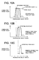
- FIGS. 10A to 10C are illustration showing process operation in another embodiment of the present invention.
- FIG. 11 is a block diagram showing a construction of the a further embodiment of the multi-path detection circuit according to the present invention.
- FIG. 12 is an illustration showing one example of a reference pattern to be used in the still further embodiment of the pattern generating portion according to the present invention.
- FIG. 1 is a block diagram showing a construction of one embodiment of a multi-path detection circuit according to the present invention.
- the shown embodiment of the multi-path detection circuit 1 is constructed with a matched filter 11 , a delay profile storage portion 12 , a maximum value retrieving portion 13 , a pattern generating portion 14 , a subtractor 15 and a counter 16 .
- the multi-path detection circuit 1 has the matched filter 11 outputting a correlation value of a spread code and a received signal.
- a delay profile of a propagation path (not shown) measured by the matched filter 11 is fed to the delay profile storage portion 12 to be stored therein.
- a first correlated peak (path) can be obtained by outputting a maximum peak position and a peak level from the delay profile by the maximum value retrieving portion 13 .
- the pattern generating portion 14 generates a logical pattern of the first correlated peak on the basis of the peak level and the peak position of the first peak obtained from the maximum value retrieving portion 13 .
- the subtractor 15 Upon detecting the second correlated peak, the subtractor 15 subtracts the logical pattern of the first correlated peak from the delay profile data in the delay profile storage portion 12 to prepare a profile from which is removed a correlated power of the first correlated peak and stores the prepared profile in the delay profile storage portion 12 . It should be noted that the subtractor 15 may be replaced with other means, such as shift register or the like as long as the profile from which is removed the correlated power of the first correlated peak can be generated.
- the maximum value retrieving portion 13 outputs the maximum peak position and the peak level to obtain the peak level and the peak position of the second correlated peak.
- the pattern generating portion 14 generates the logical pattern (logical shape) of the second correlated peak on the basis of the peak level and the peak position of the second correlated peak.
- the subtractor 15 subtracts the logical pattern of the second correlated peak from the delay profile data stored in the delay profile storage portion 12 to prepare the profile from which is removed the correlated power of the second correlated peak. Then, the prepared profile is stored in the delay profile storage portion 12 .
- a plurality of correlated peak can be retrieved. Accordingly, even if the multi-path having narrow interval between adjacent correlated peaks to cause overlapping on the delay profile, the multi-paths can be separated into respective of the correlated peaks with high precision to enable detection of the correlated peak position. Thus, reception performance can be improved.
- FIG. 2 is a block diagram showing one embodiment of the CDMA receiver according to the present invention.
- one embodiment of the CDMA receiver according to the present invention is constructed with an antenna portion 2 , a high frequency reception circuit portion (radio portion) 3 , an analog-to-digital (A/D) converter 4 , a RAKE finger portion 5 , a RAKE synthesizing portion 6 and the multi-path detection circuit 1 .
- the multi-path detection circuit 1 has the construction as shown in FIG. 1 .
- the high frequency reception circuit portion 3 is provided with a channel filter 3 a to be used for band restriction with a not shown base station.
- the data transmitted as radio wave is received by the antenna portion 2 , then is subjected to frequency conversion (down conversion) by the high frequency reception circuit portion 3 and is converted from the analog signal into digital signal by the A/D converter 4 .
- the signal from the A/D converter 4 is supplied to the multi-path detection circuit 1 for measuring the delay profile of a transmission path and timing of the multi-path is detected.
- the output of the multi-path detection circuit 1 is used as a reception timing input of the RAKE finger portion 5 . Data received at respective timing are synthesized by the RAKE Synthesizing portion 6 .
- the multi-path detection circuit 1 has the matched filter 11 outputting the correlated value of the spread code and the received signal. By this, the measured delay profile of the transmission path is stored in the delay profile storage portion 12 .
- the first correlated peak (path) can be obtained by outputting a maximum peak position and a peak level from the delay profile by the maximum value retrieving portion 13 .
- the pattern generating portion 14 generates a logical pattern of the correlated peak on the basis of the peak level and the peak position of the first correlated peak obtained from the maximum value retrieving portion 13 .
- the reference pattern (peak shape of one path of the peak level 1 ) used in the logical pattern of the correlated peak can be arithmetically derived on the basis of a coefficient used in the channel filter 3 a . From the reference pattern, the logical pattern of the correlated peak is generated on the basis of the peak level and the peak position of the correlated peak.
- the subtractor 15 Upon detecting the second correlated peak, the subtractor 15 subtracts the logical pattern of the first correlated peak from the delay profile data in the delay profile storage portion 12 to prepare a profile from which is removed a correlated power of the first correlated peak and stores the prepared profile in the delay profile storage portion 12 .
- the maximum value retrieving portion 13 outputs the maximum peak position and the peak level to obtain the peak level and the peak position of the second correlated peak.
- the pattern generating portion 14 generates the logical pattern of the second correlated peak on the basis of the peak level and the peak position of the second correlated peak.
- the subtractor 15 subtracts the logical pattern of the second correlated peak from the delay profile data stored in the delay profile storage portion 12 to prepare the profile from which is removed the correlated power of the second correlated peak. Then, the prepared profile is stored in the delay profile storage portion 12 . By repeating the foregoing operation for number of times, a plurality of correlated peak can be retrieved. It should be noted that the number of times is measured by the counter 16 .
- FIG. 3 is a block diagram showing a construction of the maximum value retrieving portion 13 of FIG. 1 .
- the maximum value retrieving portion 13 is constructed with a level comparing portion 13 a , a selector 13 b , a buffer portion(D) 13 c and a maximum position storage portion 13 d.
- the level comparing portion 3 a compares the samples of the delay profile data with the interim maximum value in the retrieved samples.
- the selector 13 b selects the same sample of the delay profile data or the interim maximum value depending upon the result of compariseon of the level comparing portion 3 a.
- the buffer portion 13 c holds an interim maximum value during maximum value retrieval.
- the maximum position storage portion 13 d holds a sample position when the level comparing portion 13 a detects new maximum value to output the maximum peak position. In the construction set forth above, all samples of the delay profile data are retrieved sequentially. At the end of search, the maximum value among all samples is stored in the buffer portion 13 c.
- FIG. 4 is a block diagram showing a construction of the pattern generating portion 14 of FIG. 1 .
- the pattern generating portion 14 is constructed with a logical pattern memory 14 a , a multiplier 14 b and a peak position setting portion 14 c.
- the logical pattern memory 14 a holds a preliminarily set reference pattern.
- the multiplier 14 b sets a peak level using the reference pattern stored in the logical pattern memory 14 a .
- the peak position setting portion 14 c sets the position of the correlated peak from a peak position input and a peak shape output (logical pattern) from the multiplier 14 b .
- the multiplier 14 b may be any other means, such as adder or the like as long as the peak level can be set using the reference pattern.
- the logical pattern memory 14 a may be realized by storing the reference pattern indicative of the logical pattern of the correlated peak [the peak shape upon one path as shown in FIG. 7A ] as set at peak level 1 in read-only-memory (ROM) or the like.
- a timing information of the multi-path thus obtained is supplied to the RAKE finger portion 5 .
- the correlated peak position can be detected with high precision to improve reception performance.
- the matched filter 11 is well known to those skilled in the art as means for measuring the delay profile. Therefore, detailed description therefor will be omitted for keeping the disclosure simple enough to facilitate clear understanding of the present invention. It should be noted that a sliding correlator may also be employed in place of the matched filter 11 . Similarly, the RAKE finger portion 5 and the RAKE synthesizing portion 6 are well known to those skilled in the art, and are not directly related to the present invention. Therefore, detailed description therefor will be omitted for keeping the disclosure simple enough to facilitate clear understanding of the present invention.
- FIGS. 5A to 5C are illustration showing examples of the delay profiles.
- FIG. 5A shows the delay profile in case of one path.
- FIG. 5B shows the delay profile in the case where interval between three paths is relatively wide.
- FIG. 5 c shows the delay profile in the case where interval between three paths is narrow.
- FIG. 6 is a flowchart showing operation of the multi-path detection circuit 1 of FIG. 1
- FIGS. 7A to 7C are illustration showing operation images of respective process for the delay profile data stored in the delay profile storage portion 12 . It should be noted that the operation shown in FIG. 6 is realized by executing a program of a not shown control memory by the multi-path detection circuit 1 .
- control memory ROM, integrated circuit (IC) memory and so forth may be used.
- FIG. 5A shows an example of the correlated peak in the case where only one path is present and only one correlated peak is present.
- the shape of the correlated peak has a width by a reception filter characteristics.
- FIG. 5B shows an example of the delay profile in which three correlated peaks are present with interval about two chips. When the correlated peaks have sufficient interval as shown, presence of the three correlated peaks is definite.
- FIG. 5C shows an example of the case in which three correlated peaks are present with interval about one chip. Since respective paths overlap to make respective peak position indefinite. Therefore, accurate detection of the position of the correlated peak is difficult in the conventional method.
- the multi-path detection circuit 1 at first, the counter 16 counting number of detected peaks is reset (step S 1 of FIG. 6 ). Subsequently, in the multi-path detection circuit 1 , the delay profile is measured by the matched filter 11 (step S 2 of FIG. 6 ). An example of the delay profile measured by the matched filter 11 is shown in FIG. 7A .
- maximum value retrieval is performed by the maximum value retrieving portion 13 (step S 3 of FIG. 6 ).
- the maximum value retrieving portion 13 outputs the detected path timing (correlated peak position) to the RAKE finger portion 5 (step S 4 of FIG. 6 ).
- the pattern generating portion 14 generates the logical pattern [see FIG. 7B ] of the detected peak on the basis of the maximum value and the peak position information detected by the maximum value retrieving portion 13 (step S 5 of FIG. 6 ).
- the subtractor 15 subtracts the logical pattern generated by the pattern generating portion 14 from the delay profile data [see FIG. 7 c ] to remove the power component of the detected peak from the delay profile data (step S 6 of FIG. 6 ).
- the delay profile storage portion 12 stores data removed the power component of the detected peak from the delay profile data by the subtractor 15 (step S 7 of FIG. 6 ). After completion of this process, the counter 16 is counted up (step S 8 of FIG. 6 ). By repeating the foregoing process for the times corresponding to number of fingers (step S 9 of FIG. 9 ), necessary number of peaks can be detected.
- the multi-path detection circuit 1 can detect timing of respective path at high precision. Therefore, reception performance can be improved.
- FIG. 8 is a block diagram showing a construction of the maximum value retrieving portion of another embodiment of the multi-path detection circuit according to the present invention.
- another embodiment of the present invention has the same construction as the maximum value retrieving portion 13 in the former embodiment of the present invention shown in FIG. 3 except for a coefficient multiplying portion 71 is provided in the maximum value retrieving portion 13 .
- Like components to those in the former embodiment will be identified by like reference numerals and detailed description therefor will be omitted for avoiding redundant discussion and whereby to keep the disclosure simple enough to facilitate clear understanding of the present invention.
- the maximum value retrieving portion 13 is constructed with the level comparing portion 13 a , the selector 13 b , buffer portion 13 c , maximum position storage portion 13 d and coefficient multiplying portion 71 .
- the level comparing portion 13 a compares the sample of the delay profile data with the interim maximum value in the retrieved samples.
- the selector 13 b selects the sample of the delay profile data and the interim maximum value depending upon the result of comparison of the level comparing portion 13 a .
- the buffer portion 13 c stores the interim maximum value during maximum value retrieval.
- all sample of the delay profile data is retrieved sequentially.
- the maximum value among all samples is stored in the buffer portion 13 c .
- the maximum position storage portion 13 d holds a sample position when the level comparing portion 13 a detects new maximum value to output the maximum peak position.
- the coefficient multiplying portion 71 multiples the maximum value among all samples stored in the buffer portion 13 c with a preliminarily set given value a to output the product to the level comparing portion 13 a and the selector 13 b.
- coefficient multiplying portion 71 may be replaced with adder or the like as long as the sample having the least delay period can be taken as the maximum point.
- FIG. 9 is a flowchart showing operation of another embodiment of the multi-path detection circuit according to the present invention.
- FIGS. 10A to 10C show example of process operation by another embodiment of the present invention. Operation and effect of another embodiment of the multi-path detection circuit according to the present invention will be discussed with reference to FIGS. 8 to 10C .
- FIG. 9 the operation shown in FIG. 9 is realized by executing a program in the not shown control memory by the multi-path detection circuit 1 .
- control memory RON, IC memory or the like may be used.
- FIG. 5C shows an example of the case in which three correlated peaks are present with interval about one chip. Since respective paths overlap to make respective peak position indefinite. Therefore, accurate detection of the position of the correlated peak is difficult in the conventional method.
- the counter 16 counting number of detected peaks is reset (step S 11 of FIG. 9 ).
- the delay profile is measured by the matched filter 11 (step S 12 of FIG. 9 ).
- maximum value retrieval and maximum position retrieval are performed by the maximum value retrieving portion 13 (steps S 13 and S 14 of FIG. 9 ).
- the maximum value retrieving portion 13 outputs the path timing (correlated peak position) to the RAKE finger portion 5 (step S 15 of FIG. 9 ).
- the pattern generating portion 14 generates the logical pattern of the detected peak on the basis of the maximum value and the peak position information detected by the maximum value retrieving portion 13 (step S 16 of FIG. 9 ).
- the subtractor 15 subtracts the logical pattern generated by the pattern generating portion 14 from the delay profile data to remove the power component of the detected peak from the delay profile data (step S 17 of FIG. 9 ).
- the delay profile storage portion 12 stores data from which is removed the power component of the detected peak from the delay profile data by the subtractor 15 (step S 18 of FIG. 9 ).
- the counter 16 is counted up (step S 19 of FIG. 9 ).
- the multi-path detection circuit 1 can detect timing of respective path at high precision. Therefore, reception performance can be improved.
- FIG. 10A shows an example of the delay profile in which a plurality of paths are located close proximity and levels of respective paths are substantially equal.
- difficulty is encountered in making judgment which sample is to be the first correlated peak, in contrast to this, in the maximum value retrieving portion 13 of the shown embodiment, as the peak of the profile, the point at the left most position (detecting position 1 ) can be selected.
- FIG. 11 is a block diagram showing a further embodiment of the multi-path detection circuit according to the present invention.
- the further embodiment of the multi-path detection circuit 8 according to the present invention has the same construction as one embodiment of the multi-path detection circuit 1 shown in FIG. 1 except for presence of a path interval judgment portion 82 and a sample subtractiong portion 83 .
- Like components to those in the former embodiment will be identified by like reference numerals and detailed description therefor will be omitted for avoiding redundant discussion and whereby to keep the disclosure simple enough to facilitate clear understanding of the present invention.
- operations of the common components are the same as those in one embodiment of the invention.
- a detection objective pattern generating portion 81 is formed by the pattern generating portion 14 and the subtractor 15 .
- the path interval judgment portion 82 makes judgment of interval of the path timing on the basis of the path timing output from the maximum value retrieving portion 13 , to drive the detection objective pattern generating portion 81 when the interval of the path timing becomes smaller than a preliminarily set interval, and to drive the sample detecting portion 83 when the interval of the path timing becomes greater than the preliminarily set interval. It should be noted that the path interval judgment portion 82 outputs the path timing output from the maximum value retrieving portion 13 as is out of the multi-path detection circuit 8 .
- the pattern generating portion 14 and the subtractor 15 in the detection objective pattern generating portion 81 perform generating operation of the delay profile data to be an object for detection.
- the sample detecting portion 83 performs similar operation as the prior art.
- pattern generating operation by the pattern generating portion 14 and the subtractor 15 is performed only for the multi-path, in which the delay profiles overlap.
- FIG. 12 is an illustration showing one example of the reference pattern to be used in the pattern generating portion in the further embodiment of the present invention.
- the delay profile before and after the wave representative of the profile peak of one path, side lobe is generated to make interval between the correlated peak narrower to cause overlap of the delay profile, these side lobe may be included in the waveform.
- the side lob portion upon generation of the reference pattern, is preliminarily prepared together with the profile peak to store as shown in FIG. 12 .
- the side lobe portion can be eliminated from the profile peak including the side lobe of adjacent profile.
- more accurate detection of the multi-path component becomes possible.
- the logical shape of the correlated peak in the delay profile is generated for detecting the correlated peak on the basis of the generated logical shape of the correlated peak to enhance precision in detection of the path timing in the multi-path environment where the correlated peaks overlap on the delay profile, to obtain better reception performance.
Abstract
Description
Claims (26)
Applications Claiming Priority (2)
| Application Number | Priority Date | Filing Date | Title |
|---|---|---|---|
| JP024559-2000 | 2000-02-02 | ||
| JP2000024559A JP3468189B2 (en) | 2000-02-02 | 2000-02-02 | Pattern generation circuit, multipath detection circuit using the same, and multipath detection method thereof |
Publications (2)
| Publication Number | Publication Date |
|---|---|
| US20010010703A1 US20010010703A1 (en) | 2001-08-02 |
| US6996157B2 true US6996157B2 (en) | 2006-02-07 |
Family
ID=18550523
Family Applications (1)
| Application Number | Title | Priority Date | Filing Date |
|---|---|---|---|
| US09/770,506 Expired - Fee Related US6996157B2 (en) | 2000-02-02 | 2001-01-29 | Pattern generation circuit, multi-path detection circuit employing the same and multi-path detection method |
Country Status (7)
| Country | Link |
|---|---|
| US (1) | US6996157B2 (en) |
| EP (1) | EP1126626B1 (en) |
| JP (1) | JP3468189B2 (en) |
| CN (1) | CN1196290C (en) |
| AU (1) | AU780497B2 (en) |
| DE (1) | DE60125437T2 (en) |
| HK (1) | HK1038842A1 (en) |
Cited By (17)
| Publication number | Priority date | Publication date | Assignee | Title |
|---|---|---|---|---|
| US20030235241A1 (en) * | 2002-06-19 | 2003-12-25 | Koichi Tamura | CDMA demodulation circuit, CDMA mobile communication demodulation method used therefor, and storage medium recording program thereof |
| US20040151232A1 (en) * | 2001-05-08 | 2004-08-05 | Reinhold Braam | Method for detecting multipath signals |
| US20040156426A1 (en) * | 2002-03-14 | 2004-08-12 | Katsuyuki Motoyoshi | Spread spectrum receiver |
| US20040213363A1 (en) * | 2003-04-28 | 2004-10-28 | Bottomley Gregory Edward | Methods and receivers that estimate multi-path delays by removing signal rays from a power-delay profile |
| US20060176937A1 (en) * | 2005-01-20 | 2006-08-10 | Mauro Bottero | Method for rake finger placement with reliable path detection |
| US20060200553A1 (en) * | 2004-12-14 | 2006-09-07 | Jian Xu | Path searching method of a wireless communication system and path searching apparatus thereof |
| US20090149211A1 (en) * | 2007-11-05 | 2009-06-11 | Picochip Designs Limited | Power control |
| US20110002426A1 (en) * | 2009-01-05 | 2011-01-06 | Picochip Designs Limited | Rake Receiver |
| US8463312B2 (en) | 2009-06-05 | 2013-06-11 | Mindspeed Technologies U.K., Limited | Method and device in a communication network |
| US8712469B2 (en) | 2011-05-16 | 2014-04-29 | Mindspeed Technologies U.K., Limited | Accessing a base station |
| US8798630B2 (en) | 2009-10-05 | 2014-08-05 | Intel Corporation | Femtocell base station |
| US8849340B2 (en) | 2009-05-07 | 2014-09-30 | Intel Corporation | Methods and devices for reducing interference in an uplink |
| US8862076B2 (en) | 2009-06-05 | 2014-10-14 | Intel Corporation | Method and device in a communication network |
| US8904148B2 (en) | 2000-12-19 | 2014-12-02 | Intel Corporation | Processor architecture with switch matrices for transferring data along buses |
| US9042434B2 (en) | 2011-04-05 | 2015-05-26 | Intel Corporation | Filter |
| US9107136B2 (en) | 2010-08-16 | 2015-08-11 | Intel Corporation | Femtocell access control |
| US10856302B2 (en) | 2011-04-05 | 2020-12-01 | Intel Corporation | Multimode base station |
Families Citing this family (19)
| Publication number | Priority date | Publication date | Assignee | Title |
|---|---|---|---|---|
| JP3510589B2 (en) | 2000-12-15 | 2004-03-29 | Necエレクトロニクス株式会社 | Cell search method and cell search device |
| US7065064B2 (en) * | 2001-12-20 | 2006-06-20 | Interdigital Technology Corporation | Cell search using peak quality factors |
| CN1173509C (en) | 2001-12-30 | 2004-10-27 | 华为技术有限公司 | Identification method of visible and non-visible channel in CDMA mobile communication system |
| JP3856126B2 (en) * | 2002-05-21 | 2006-12-13 | 日本電気株式会社 | Path timing detection method, path timing detection apparatus, and adaptive array antenna system |
| JP2004297307A (en) * | 2003-03-26 | 2004-10-21 | Matsushita Electric Ind Co Ltd | Apparatus and method for detecting path |
| US7239677B2 (en) | 2003-04-29 | 2007-07-03 | Telefonaktiebolaget L M Ericsson (Publ) | Method and apparatus for soft symbol scaling |
| US7116998B2 (en) | 2003-05-14 | 2006-10-03 | Telefonaktiebolaget L M Ericsson (Publ) | Subtractive multipath delay detection |
| CN100527654C (en) | 2003-05-28 | 2009-08-12 | 华为技术有限公司 | Method for determining first path precisively in CDMA mobile communiation system |
| JP4097615B2 (en) * | 2004-03-23 | 2008-06-11 | 三洋電機株式会社 | Signal detection method and apparatus, and transmission apparatus and reception apparatus using the same |
| JP4627008B2 (en) * | 2004-05-13 | 2011-02-09 | 株式会社エヌ・ティ・ティ・ドコモ | Path searcher and path search method |
| ATE535060T1 (en) | 2004-05-13 | 2011-12-15 | Ntt Docomo Inc | APPARATUS AND METHOD FOR PATH SEARCHING IN A CDMA RECEIVER |
| KR100941553B1 (en) | 2005-02-25 | 2010-02-10 | 닛본 덴끼 가부시끼가이샤 | Transmission line estimating device, cdma receiving device, and transmission line estimating method |
| US20090073956A1 (en) * | 2005-05-18 | 2009-03-19 | Koichi Tamura | Path search processing circuit, path search method, and control program |
| JP4720439B2 (en) * | 2005-11-02 | 2011-07-13 | 日本電気株式会社 | Mobile communication demodulation circuit and path search method used therefor |
| SG136813A1 (en) * | 2006-04-11 | 2007-11-29 | Sony Corp | A method for estimating one or more parameters of a ultra wideband signal and a receiver system for receiving ultra wideband signals |
| JP4925424B2 (en) * | 2006-09-05 | 2012-04-25 | 日本放送協会 | Delay profile measuring device |
| BRPI0720832A2 (en) * | 2007-01-18 | 2013-01-29 | Thomson Licensing | Method for synchronizing received digital signal symbols and digital signal receiver using the same method |
| KR101625217B1 (en) * | 2014-12-30 | 2016-06-07 | 한국해양과학기술원 | Apparatus and method for estimating doppler shift in underwater communication |
| US10158436B2 (en) * | 2015-02-17 | 2018-12-18 | Mitsubishi Electric Corporation | Receiver apparatus and reception method |
Citations (15)
| Publication number | Priority date | Publication date | Assignee | Title |
|---|---|---|---|---|
| JPH0832553A (en) | 1994-07-19 | 1996-02-02 | Matsushita Electric Ind Co Ltd | Spread spectrum communication equipment |
| JPH08181636A (en) | 1994-12-22 | 1996-07-12 | Nec Corp | Inverse spread code phase detector in ss receiver |
| JPH09270735A (en) | 1996-01-30 | 1997-10-14 | Sharp Corp | Spread spectrum communication reception method |
| EP0814573A2 (en) | 1996-06-21 | 1997-12-29 | Nec Corporation | Path-diversity CDMA reception by detecting lower-peak correlation sequence following removal of higher-peak sequences |
| JPH10308688A (en) | 1997-05-02 | 1998-11-17 | Nec Corp | Reception device for spread spectrum communication |
| JPH10336072A (en) | 1997-06-02 | 1998-12-18 | N T T Ido Tsushinmo Kk | Rake receiver for direct diffusion cdma transmission system |
| WO1999035763A1 (en) | 1998-01-12 | 1999-07-15 | Ericsson Inc. | Method and apparatus for multipath delay estimation in direct sequence spread spectrum communication systems |
| US5960028A (en) | 1995-08-11 | 1999-09-28 | Sharp Kabushiki Kaisha | Spread spectrum communication system |
| WO2000004648A1 (en) | 1998-07-16 | 2000-01-27 | Telefonaktiebolaget Lm Ericsson (Publ) | Adaptive path selection threshold setting for ds-cdma receivers |
| JP2000101549A (en) | 1998-09-24 | 2000-04-07 | Nec Corp | Cdma receiver, path detection method used therefor and recording medium recorded with control program therefor |
| JP2000252871A (en) | 1999-03-01 | 2000-09-14 | Sony Corp | Method and device for receiving |
| JP2000269860A (en) | 1999-03-17 | 2000-09-29 | Yrp Mobile Telecommunications Key Tech Res Lab Co Ltd | User timing detector for spread code with guard chip and spread spectrum receiver |
| JP2000278177A (en) | 1999-03-19 | 2000-10-06 | Sanyo Electric Co Ltd | Valid path detector |
| WO2000064065A1 (en) | 1999-04-16 | 2000-10-26 | Matsushita Electric Industrial Co., Ltd. | Receiver and synchronous acquisition method |
| JP2001203608A (en) | 2000-01-19 | 2001-07-27 | Mitsubishi Electric Corp | Spread spectrum receiver, and spread spectrum reception method |
-
2000
- 2000-02-02 JP JP2000024559A patent/JP3468189B2/en not_active Expired - Fee Related
-
2001
- 2001-01-29 US US09/770,506 patent/US6996157B2/en not_active Expired - Fee Related
- 2001-02-01 AU AU16765/01A patent/AU780497B2/en not_active Ceased
- 2001-02-01 DE DE2001625437 patent/DE60125437T2/en not_active Expired - Lifetime
- 2001-02-01 EP EP20010102329 patent/EP1126626B1/en not_active Expired - Lifetime
- 2001-02-02 CN CNB011023392A patent/CN1196290C/en not_active Expired - Fee Related
-
2002
- 2002-01-14 HK HK02100241.5A patent/HK1038842A1/en unknown
Patent Citations (19)
| Publication number | Priority date | Publication date | Assignee | Title |
|---|---|---|---|---|
| JPH0832553A (en) | 1994-07-19 | 1996-02-02 | Matsushita Electric Ind Co Ltd | Spread spectrum communication equipment |
| US5812593A (en) | 1994-12-22 | 1998-09-22 | Nec Corporation | De-spread code phase detection apparatus in spread spectrum type receiver |
| JPH08181636A (en) | 1994-12-22 | 1996-07-12 | Nec Corp | Inverse spread code phase detector in ss receiver |
| US5960028A (en) | 1995-08-11 | 1999-09-28 | Sharp Kabushiki Kaisha | Spread spectrum communication system |
| JPH09270735A (en) | 1996-01-30 | 1997-10-14 | Sharp Corp | Spread spectrum communication reception method |
| EP0814573A2 (en) | 1996-06-21 | 1997-12-29 | Nec Corporation | Path-diversity CDMA reception by detecting lower-peak correlation sequence following removal of higher-peak sequences |
| US6181732B1 (en) | 1997-02-05 | 2001-01-30 | Nec Corporation | Receiving apparatus for spectrum spreading and receiving method |
| JPH10308688A (en) | 1997-05-02 | 1998-11-17 | Nec Corp | Reception device for spread spectrum communication |
| JPH10336072A (en) | 1997-06-02 | 1998-12-18 | N T T Ido Tsushinmo Kk | Rake receiver for direct diffusion cdma transmission system |
| WO1999035763A1 (en) | 1998-01-12 | 1999-07-15 | Ericsson Inc. | Method and apparatus for multipath delay estimation in direct sequence spread spectrum communication systems |
| WO2000004648A1 (en) | 1998-07-16 | 2000-01-27 | Telefonaktiebolaget Lm Ericsson (Publ) | Adaptive path selection threshold setting for ds-cdma receivers |
| JP2000101549A (en) | 1998-09-24 | 2000-04-07 | Nec Corp | Cdma receiver, path detection method used therefor and recording medium recorded with control program therefor |
| JP2000252871A (en) | 1999-03-01 | 2000-09-14 | Sony Corp | Method and device for receiving |
| US6519451B1 (en) | 1999-03-01 | 2003-02-11 | Sony Corporation | Receiving method and receiving apparatus |
| JP2000269860A (en) | 1999-03-17 | 2000-09-29 | Yrp Mobile Telecommunications Key Tech Res Lab Co Ltd | User timing detector for spread code with guard chip and spread spectrum receiver |
| JP2000278177A (en) | 1999-03-19 | 2000-10-06 | Sanyo Electric Co Ltd | Valid path detector |
| WO2000064065A1 (en) | 1999-04-16 | 2000-10-26 | Matsushita Electric Industrial Co., Ltd. | Receiver and synchronous acquisition method |
| EP1096694A1 (en) | 1999-04-16 | 2001-05-02 | Matsushita Electric Industrial Co., Ltd. | Receiver and synchronous acquisition method |
| JP2001203608A (en) | 2000-01-19 | 2001-07-27 | Mitsubishi Electric Corp | Spread spectrum receiver, and spread spectrum reception method |
Non-Patent Citations (2)
| Title |
|---|
| Akio Aoyama et al., "Path-search Performance of DS-CDMA System in Laboratory and Field Experiments.", Technical Report of The Institute of Electronics, Information and Communication Engineers (IEICE), RCS97-164, (Nov. 1997), pp. 51-58, C&C Media Research Lab., NEC Corporation. |
| Essam Sourour, Gregory Bottomley and Rajaram Ramesh, "Delay Tracking For Direct Sequence Spread Spectrum Systems In Multipath Fading Channels," 1999 IEEE, Ericsson Inc., Page 422-426. |
Cited By (25)
| Publication number | Priority date | Publication date | Assignee | Title |
|---|---|---|---|---|
| US8904148B2 (en) | 2000-12-19 | 2014-12-02 | Intel Corporation | Processor architecture with switch matrices for transferring data along buses |
| US20040151232A1 (en) * | 2001-05-08 | 2004-08-05 | Reinhold Braam | Method for detecting multipath signals |
| US7292621B2 (en) * | 2001-05-08 | 2007-11-06 | Siemens Aktiengesellschaft | Method for detecting multipath signals |
| US7280587B2 (en) * | 2002-03-14 | 2007-10-09 | Mitsubishi Denki Kabushiki Kaisha | Spectrum spread reception apparatus |
| US20040156426A1 (en) * | 2002-03-14 | 2004-08-12 | Katsuyuki Motoyoshi | Spread spectrum receiver |
| US20030235241A1 (en) * | 2002-06-19 | 2003-12-25 | Koichi Tamura | CDMA demodulation circuit, CDMA mobile communication demodulation method used therefor, and storage medium recording program thereof |
| US7313169B2 (en) * | 2002-06-19 | 2007-12-25 | Nec Corporation | CDMA demodulation circuit, CDMA mobile communication demodulation method used therefor, and storage medium recording program thereof |
| US7212591B2 (en) * | 2003-04-28 | 2007-05-01 | Telefonaktiebolaget Lm Ericsson (Publ) | Methods and receivers that estimate multi-path delays by removing signal rays from a power-delay profile |
| US20040213363A1 (en) * | 2003-04-28 | 2004-10-28 | Bottomley Gregory Edward | Methods and receivers that estimate multi-path delays by removing signal rays from a power-delay profile |
| US20060200553A1 (en) * | 2004-12-14 | 2006-09-07 | Jian Xu | Path searching method of a wireless communication system and path searching apparatus thereof |
| US20060176937A1 (en) * | 2005-01-20 | 2006-08-10 | Mauro Bottero | Method for rake finger placement with reliable path detection |
| US20090149211A1 (en) * | 2007-11-05 | 2009-06-11 | Picochip Designs Limited | Power control |
| US8559998B2 (en) | 2007-11-05 | 2013-10-15 | Mindspeed Technologies U.K., Limited | Power control |
| US20110002426A1 (en) * | 2009-01-05 | 2011-01-06 | Picochip Designs Limited | Rake Receiver |
| US20140044223A1 (en) * | 2009-01-05 | 2014-02-13 | Mindspeed Technologies U.K., Limited | Rake Receiver |
| US8849340B2 (en) | 2009-05-07 | 2014-09-30 | Intel Corporation | Methods and devices for reducing interference in an uplink |
| US8463312B2 (en) | 2009-06-05 | 2013-06-11 | Mindspeed Technologies U.K., Limited | Method and device in a communication network |
| US8862076B2 (en) | 2009-06-05 | 2014-10-14 | Intel Corporation | Method and device in a communication network |
| US8892154B2 (en) | 2009-06-05 | 2014-11-18 | Intel Corporation | Method and device in a communication network |
| US9807771B2 (en) | 2009-06-05 | 2017-10-31 | Intel Corporation | Method and device in a communication network |
| US8798630B2 (en) | 2009-10-05 | 2014-08-05 | Intel Corporation | Femtocell base station |
| US9107136B2 (en) | 2010-08-16 | 2015-08-11 | Intel Corporation | Femtocell access control |
| US9042434B2 (en) | 2011-04-05 | 2015-05-26 | Intel Corporation | Filter |
| US10856302B2 (en) | 2011-04-05 | 2020-12-01 | Intel Corporation | Multimode base station |
| US8712469B2 (en) | 2011-05-16 | 2014-04-29 | Mindspeed Technologies U.K., Limited | Accessing a base station |
Also Published As
| Publication number | Publication date |
|---|---|
| EP1126626A3 (en) | 2004-03-03 |
| US20010010703A1 (en) | 2001-08-02 |
| AU1676501A (en) | 2001-08-09 |
| CN1316842A (en) | 2001-10-10 |
| AU780497B2 (en) | 2005-03-24 |
| EP1126626B1 (en) | 2006-12-27 |
| EP1126626A2 (en) | 2001-08-22 |
| JP3468189B2 (en) | 2003-11-17 |
| CN1196290C (en) | 2005-04-06 |
| DE60125437D1 (en) | 2007-02-08 |
| HK1038842A1 (en) | 2002-03-28 |
| DE60125437T2 (en) | 2007-10-11 |
| JP2001217747A (en) | 2001-08-10 |
Similar Documents
| Publication | Publication Date | Title |
|---|---|---|
| US6996157B2 (en) | Pattern generation circuit, multi-path detection circuit employing the same and multi-path detection method | |
| US7072383B2 (en) | Path search method of spread spectrum communication system and receiver using the method | |
| EP2182645B1 (en) | Method and system for spread spectrum signal acquisition | |
| EP0989685A2 (en) | CDMA rake receiver | |
| JP3943062B2 (en) | CDMA receiving apparatus, CDMA receiving method, CDMA receiving program, and program recording medium | |
| US7075974B2 (en) | Multi-path detection circuit and method for a CDMA receiver | |
| EP2213009B1 (en) | Frequency offset estimation in a cdma system | |
| AU7925200A (en) | Signal acquisition system for spread spectrum receiver | |
| KR20010102972A (en) | Sequential-acquisition, multi-band, multi-channel, matched filter | |
| KR100458665B1 (en) | Cdma receiver, path search method and computer-readable storage medium having program for executing path search method recorded thereon | |
| US8175137B2 (en) | Method of processing a digital signal derived from a direct-sequence spread spectrum signal | |
| US7406115B2 (en) | Method for evaluating spread spectrum radar and spread spectrum radar | |
| US7957455B2 (en) | Method and circuit arrangement for calibration of a sampling control signal which influences the sampling time of a received signal from a sampling phase selection element | |
| AU2004202130B2 (en) | Pattern Generation Circuit, Multi-path Detection Circuit Employing the Same and Multi-path Detection Method | |
| US7342953B2 (en) | Synchronization detection circuit | |
| EP3043484B1 (en) | Apparatus and method for compensating for timing offset in spread spectrum system | |
| JP3593021B2 (en) | Synchronous acquisition system | |
| KR19990024953A (en) | Impulse response measurement device of CDM system |
Legal Events
| Date | Code | Title | Description |
|---|---|---|---|
| AS | Assignment |
Owner name: NEC CORPORATION, JAPAN Free format text: ASSIGNMENT OF ASSIGNORS INTEREST;ASSIGNOR:OHSUGE, MICHIHIRO;REEL/FRAME:011491/0219 Effective date: 20010119 |
|
| FEPP | Fee payment procedure |
Free format text: PAYOR NUMBER ASSIGNED (ORIGINAL EVENT CODE: ASPN); ENTITY STATUS OF PATENT OWNER: LARGE ENTITY |
|
| FPAY | Fee payment |
Year of fee payment: 4 |
|
| AS | Assignment |
Owner name: WARREN & LEWIS INVESTMENT CORPORATION, VIRGINIA Free format text: ASSIGNMENT OF ASSIGNORS INTEREST;ASSIGNOR:NEC CORPORATION;REEL/FRAME:029216/0855 Effective date: 20120903 |
|
| REMI | Maintenance fee reminder mailed | ||
| LAPS | Lapse for failure to pay maintenance fees | ||
| STCH | Information on status: patent discontinuation |
Free format text: PATENT EXPIRED DUE TO NONPAYMENT OF MAINTENANCE FEES UNDER 37 CFR 1.362 |
|
| FP | Lapsed due to failure to pay maintenance fee |
Effective date: 20140207 |
|
| AS | Assignment |
Owner name: NEC CORPORATION, JAPAN Free format text: NOTICE OF TERMINATION;ASSIGNOR:WARREN & LEWIS INVESTMENT CORPORATION;REEL/FRAME:034244/0623 Effective date: 20141113 |
|
| AS | Assignment |
Owner name: NEC CORPORATION, JAPAN Free format text: NUNC PRO TUNC ASSIGNMENT;ASSIGNORS:WARREN & LEWIS INVESTMENT CORPORATION;COMMIX SYSTEMS, LCC;REEL/FRAME:037209/0592 Effective date: 20151019 |
|
| AS | Assignment |
Owner name: NEC CORPORATION, JAPAN Free format text: CORRECTIVE ASSIGNMENT TO CORRECT THE SECOND CONVEYING PARTY NAME PREVIOUSLY RECORDED AT REEL: 037209 FRAME: 0592. ASSIGNOR(S) HEREBY CONFIRMS THE ASSIGNMENT;ASSIGNORS:WARREN & LEWIS INVESTMENT CORPORATION;COMMIX SYSTEMS, LLC;REEL/FRAME:037279/0685 Effective date: 20151019 |