US6998620B2 - Stable energy detector for extreme ultraviolet radiation detection - Google Patents
Stable energy detector for extreme ultraviolet radiation detection Download PDFInfo
- Publication number
- US6998620B2 US6998620B2 US10/218,690 US21869002A US6998620B2 US 6998620 B2 US6998620 B2 US 6998620B2 US 21869002 A US21869002 A US 21869002A US 6998620 B2 US6998620 B2 US 6998620B2
- Authority
- US
- United States
- Prior art keywords
- detector
- euv
- beam component
- detector element
- radiation
- Prior art date
- Legal status (The legal status is an assumption and is not a legal conclusion. Google has not performed a legal analysis and makes no representation as to the accuracy of the status listed.)
- Expired - Lifetime, expires
Links
- 230000005855 radiation Effects 0.000 title claims description 63
- 238000001514 detection method Methods 0.000 title description 2
- 230000003287 optical effect Effects 0.000 claims abstract description 18
- 230000007774 longterm Effects 0.000 claims abstract description 7
- 230000004888 barrier function Effects 0.000 claims abstract description 4
- 230000006798 recombination Effects 0.000 claims abstract description 4
- 238000005215 recombination Methods 0.000 claims abstract description 4
- 238000012544 monitoring process Methods 0.000 claims description 13
- 238000000034 method Methods 0.000 claims description 10
- 230000008569 process Effects 0.000 claims description 7
- 238000012545 processing Methods 0.000 claims description 5
- 239000011888 foil Substances 0.000 claims description 2
- 239000007789 gas Substances 0.000 description 32
- ZXEYZECDXFPJRJ-UHFFFAOYSA-N $l^{3}-silane;platinum Chemical compound [SiH3].[Pt] ZXEYZECDXFPJRJ-UHFFFAOYSA-N 0.000 description 21
- 229910021339 platinum silicide Inorganic materials 0.000 description 20
- 238000001900 extreme ultraviolet lithography Methods 0.000 description 8
- 241000894007 species Species 0.000 description 8
- 239000002245 particle Substances 0.000 description 7
- 230000036278 prepulse Effects 0.000 description 7
- 238000010926 purge Methods 0.000 description 7
- 230000000694 effects Effects 0.000 description 6
- 239000007787 solid Substances 0.000 description 6
- 239000000463 material Substances 0.000 description 5
- 230000003595 spectral effect Effects 0.000 description 5
- XKRFYHLGVUSROY-UHFFFAOYSA-N Argon Chemical compound [Ar] XKRFYHLGVUSROY-UHFFFAOYSA-N 0.000 description 4
- 230000006872 improvement Effects 0.000 description 4
- 239000011261 inert gas Substances 0.000 description 4
- 238000002310 reflectometry Methods 0.000 description 4
- 229910052710 silicon Inorganic materials 0.000 description 4
- PXGOKWXKJXAPGV-UHFFFAOYSA-N Fluorine Chemical compound FF PXGOKWXKJXAPGV-UHFFFAOYSA-N 0.000 description 3
- XUIMIQQOPSSXEZ-UHFFFAOYSA-N Silicon Chemical compound [Si] XUIMIQQOPSSXEZ-UHFFFAOYSA-N 0.000 description 3
- 238000001015 X-ray lithography Methods 0.000 description 3
- 239000000356 contaminant Substances 0.000 description 3
- 238000013461 design Methods 0.000 description 3
- 238000001459 lithography Methods 0.000 description 3
- 238000000926 separation method Methods 0.000 description 3
- 239000010703 silicon Substances 0.000 description 3
- 230000002123 temporal effect Effects 0.000 description 3
- 229910052724 xenon Inorganic materials 0.000 description 3
- FHNFHKCVQCLJFQ-UHFFFAOYSA-N xenon atom Chemical compound [Xe] FHNFHKCVQCLJFQ-UHFFFAOYSA-N 0.000 description 3
- IJGRMHOSHXDMSA-UHFFFAOYSA-N Atomic nitrogen Chemical compound N#N IJGRMHOSHXDMSA-UHFFFAOYSA-N 0.000 description 2
- YZCKVEUIGOORGS-OUBTZVSYSA-N Deuterium Chemical compound [2H] YZCKVEUIGOORGS-OUBTZVSYSA-N 0.000 description 2
- WHXSMMKQMYFTQS-UHFFFAOYSA-N Lithium Chemical compound [Li] WHXSMMKQMYFTQS-UHFFFAOYSA-N 0.000 description 2
- PNEYBMLMFCGWSK-UHFFFAOYSA-N aluminium oxide Inorganic materials [O-2].[O-2].[O-2].[Al+3].[Al+3] PNEYBMLMFCGWSK-UHFFFAOYSA-N 0.000 description 2
- 229910052786 argon Inorganic materials 0.000 description 2
- QVGXLLKOCUKJST-UHFFFAOYSA-N atomic oxygen Chemical compound [O] QVGXLLKOCUKJST-UHFFFAOYSA-N 0.000 description 2
- 230000008901 benefit Effects 0.000 description 2
- 229910052790 beryllium Inorganic materials 0.000 description 2
- ATBAMAFKBVZNFJ-UHFFFAOYSA-N beryllium atom Chemical compound [Be] ATBAMAFKBVZNFJ-UHFFFAOYSA-N 0.000 description 2
- 238000000576 coating method Methods 0.000 description 2
- 230000008878 coupling Effects 0.000 description 2
- 238000010168 coupling process Methods 0.000 description 2
- 238000005859 coupling reaction Methods 0.000 description 2
- 229910052805 deuterium Inorganic materials 0.000 description 2
- 239000003085 diluting agent Substances 0.000 description 2
- 239000000428 dust Substances 0.000 description 2
- 230000004907 flux Effects 0.000 description 2
- 239000001307 helium Substances 0.000 description 2
- 229910052734 helium Inorganic materials 0.000 description 2
- SWQJXJOGLNCZEY-UHFFFAOYSA-N helium atom Chemical compound [He] SWQJXJOGLNCZEY-UHFFFAOYSA-N 0.000 description 2
- 238000003384 imaging method Methods 0.000 description 2
- 238000003780 insertion Methods 0.000 description 2
- 230000037431 insertion Effects 0.000 description 2
- 229910052744 lithium Inorganic materials 0.000 description 2
- 230000007246 mechanism Effects 0.000 description 2
- 239000000203 mixture Substances 0.000 description 2
- 239000001301 oxygen Substances 0.000 description 2
- 229910052760 oxygen Inorganic materials 0.000 description 2
- 238000000206 photolithography Methods 0.000 description 2
- 239000012716 precipitator Substances 0.000 description 2
- 230000035945 sensitivity Effects 0.000 description 2
- 230000005461 Bremsstrahlung Effects 0.000 description 1
- 229910003178 Mo2C Inorganic materials 0.000 description 1
- ZOKXTWBITQBERF-UHFFFAOYSA-N Molybdenum Chemical compound [Mo] ZOKXTWBITQBERF-UHFFFAOYSA-N 0.000 description 1
- 244000000188 Vaccinium ovalifolium Species 0.000 description 1
- QCWXUUIWCKQGHC-UHFFFAOYSA-N Zirconium Chemical compound [Zr] QCWXUUIWCKQGHC-UHFFFAOYSA-N 0.000 description 1
- 239000006096 absorbing agent Substances 0.000 description 1
- 238000010521 absorption reaction Methods 0.000 description 1
- 238000009825 accumulation Methods 0.000 description 1
- 230000006978 adaptation Effects 0.000 description 1
- 230000002411 adverse Effects 0.000 description 1
- XAGFODPZIPBFFR-UHFFFAOYSA-N aluminium Chemical compound [Al] XAGFODPZIPBFFR-UHFFFAOYSA-N 0.000 description 1
- 229910052782 aluminium Inorganic materials 0.000 description 1
- 238000000149 argon plasma sintering Methods 0.000 description 1
- 230000005540 biological transmission Effects 0.000 description 1
- 230000015572 biosynthetic process Effects 0.000 description 1
- 239000003990 capacitor Substances 0.000 description 1
- 230000015556 catabolic process Effects 0.000 description 1
- 229910010293 ceramic material Inorganic materials 0.000 description 1
- RZVXOCDCIIFGGH-UHFFFAOYSA-N chromium gold Chemical compound [Cr].[Au] RZVXOCDCIIFGGH-UHFFFAOYSA-N 0.000 description 1
- 239000011248 coating agent Substances 0.000 description 1
- 230000002596 correlated effect Effects 0.000 description 1
- 229910052593 corundum Inorganic materials 0.000 description 1
- 229910021419 crystalline silicon Inorganic materials 0.000 description 1
- 230000007547 defect Effects 0.000 description 1
- 238000006731 degradation reaction Methods 0.000 description 1
- 238000011161 development Methods 0.000 description 1
- 230000005684 electric field Effects 0.000 description 1
- 238000005516 engineering process Methods 0.000 description 1
- 238000011156 evaluation Methods 0.000 description 1
- 230000001747 exhibiting effect Effects 0.000 description 1
- 238000002474 experimental method Methods 0.000 description 1
- 239000012530 fluid Substances 0.000 description 1
- 239000001257 hydrogen Substances 0.000 description 1
- 229910052739 hydrogen Inorganic materials 0.000 description 1
- 150000002431 hydrogen Chemical class 0.000 description 1
- 238000005286 illumination Methods 0.000 description 1
- 238000010348 incorporation Methods 0.000 description 1
- 239000012212 insulator Substances 0.000 description 1
- 238000011835 investigation Methods 0.000 description 1
- 150000002500 ions Chemical class 0.000 description 1
- 229910052743 krypton Inorganic materials 0.000 description 1
- DNNSSWSSYDEUBZ-UHFFFAOYSA-N krypton atom Chemical compound [Kr] DNNSSWSSYDEUBZ-UHFFFAOYSA-N 0.000 description 1
- 238000004519 manufacturing process Methods 0.000 description 1
- 238000012986 modification Methods 0.000 description 1
- 230000004048 modification Effects 0.000 description 1
- 229910052750 molybdenum Inorganic materials 0.000 description 1
- 239000011733 molybdenum Substances 0.000 description 1
- 238000012806 monitoring device Methods 0.000 description 1
- 229910052754 neon Inorganic materials 0.000 description 1
- GKAOGPIIYCISHV-UHFFFAOYSA-N neon atom Chemical compound [Ne] GKAOGPIIYCISHV-UHFFFAOYSA-N 0.000 description 1
- 229910052758 niobium Inorganic materials 0.000 description 1
- 239000010955 niobium Substances 0.000 description 1
- GUCVJGMIXFAOAE-UHFFFAOYSA-N niobium atom Chemical compound [Nb] GUCVJGMIXFAOAE-UHFFFAOYSA-N 0.000 description 1
- 229910052757 nitrogen Inorganic materials 0.000 description 1
- 229910052756 noble gas Inorganic materials 0.000 description 1
- 230000000149 penetrating effect Effects 0.000 description 1
- 238000000746 purification Methods 0.000 description 1
- 238000011160 research Methods 0.000 description 1
- 229910052594 sapphire Inorganic materials 0.000 description 1
- 239000010980 sapphire Substances 0.000 description 1
- 239000004065 semiconductor Substances 0.000 description 1
- 230000002269 spontaneous effect Effects 0.000 description 1
- 239000000758 substrate Substances 0.000 description 1
- 238000012360 testing method Methods 0.000 description 1
- 238000012795 verification Methods 0.000 description 1
- 238000004846 x-ray emission Methods 0.000 description 1
- 238000003963 x-ray microscopy Methods 0.000 description 1
- 229910001845 yogo sapphire Inorganic materials 0.000 description 1
- 229910052727 yttrium Inorganic materials 0.000 description 1
- VWQVUPCCIRVNHF-UHFFFAOYSA-N yttrium atom Chemical compound [Y] VWQVUPCCIRVNHF-UHFFFAOYSA-N 0.000 description 1
- 229910052726 zirconium Inorganic materials 0.000 description 1
Images


Classifications
-
- G—PHYSICS
- G01—MEASURING; TESTING
- G01J—MEASUREMENT OF INTENSITY, VELOCITY, SPECTRAL CONTENT, POLARISATION, PHASE OR PULSE CHARACTERISTICS OF INFRARED, VISIBLE OR ULTRAVIOLET LIGHT; COLORIMETRY; RADIATION PYROMETRY
- G01J1/00—Photometry, e.g. photographic exposure meter
- G01J1/42—Photometry, e.g. photographic exposure meter using electric radiation detectors
- G01J1/429—Photometry, e.g. photographic exposure meter using electric radiation detectors applied to measurement of ultraviolet light
-
- B—PERFORMING OPERATIONS; TRANSPORTING
- B82—NANOTECHNOLOGY
- B82Y—SPECIFIC USES OR APPLICATIONS OF NANOSTRUCTURES; MEASUREMENT OR ANALYSIS OF NANOSTRUCTURES; MANUFACTURE OR TREATMENT OF NANOSTRUCTURES
- B82Y10/00—Nanotechnology for information processing, storage or transmission, e.g. quantum computing or single electron logic
-
- G—PHYSICS
- G03—PHOTOGRAPHY; CINEMATOGRAPHY; ANALOGOUS TECHNIQUES USING WAVES OTHER THAN OPTICAL WAVES; ELECTROGRAPHY; HOLOGRAPHY
- G03F—PHOTOMECHANICAL PRODUCTION OF TEXTURED OR PATTERNED SURFACES, e.g. FOR PRINTING, FOR PROCESSING OF SEMICONDUCTOR DEVICES; MATERIALS THEREFOR; ORIGINALS THEREFOR; APPARATUS SPECIALLY ADAPTED THEREFOR
- G03F7/00—Photomechanical, e.g. photolithographic, production of textured or patterned surfaces, e.g. printing surfaces; Materials therefor, e.g. comprising photoresists; Apparatus specially adapted therefor
- G03F7/70—Microphotolithographic exposure; Apparatus therefor
- G03F7/70008—Production of exposure light, i.e. light sources
- G03F7/70033—Production of exposure light, i.e. light sources by plasma extreme ultraviolet [EUV] sources
-
- G—PHYSICS
- G03—PHOTOGRAPHY; CINEMATOGRAPHY; ANALOGOUS TECHNIQUES USING WAVES OTHER THAN OPTICAL WAVES; ELECTROGRAPHY; HOLOGRAPHY
- G03F—PHOTOMECHANICAL PRODUCTION OF TEXTURED OR PATTERNED SURFACES, e.g. FOR PRINTING, FOR PROCESSING OF SEMICONDUCTOR DEVICES; MATERIALS THEREFOR; ORIGINALS THEREFOR; APPARATUS SPECIALLY ADAPTED THEREFOR
- G03F7/00—Photomechanical, e.g. photolithographic, production of textured or patterned surfaces, e.g. printing surfaces; Materials therefor, e.g. comprising photoresists; Apparatus specially adapted therefor
- G03F7/70—Microphotolithographic exposure; Apparatus therefor
- G03F7/70483—Information management; Active and passive control; Testing; Wafer monitoring, e.g. pattern monitoring
- G03F7/7055—Exposure light control in all parts of the microlithographic apparatus, e.g. pulse length control or light interruption
- G03F7/70558—Dose control, i.e. achievement of a desired dose
-
- H—ELECTRICITY
- H01—ELECTRIC ELEMENTS
- H01L—SEMICONDUCTOR DEVICES NOT COVERED BY CLASS H10
- H01L31/00—Semiconductor devices sensitive to infrared radiation, light, electromagnetic radiation of shorter wavelength or corpuscular radiation and specially adapted either for the conversion of the energy of such radiation into electrical energy or for the control of electrical energy by such radiation; Processes or apparatus specially adapted for the manufacture or treatment thereof or of parts thereof; Details thereof
- H01L31/02—Details
- H01L31/0216—Coatings
- H01L31/02161—Coatings for devices characterised by at least one potential jump barrier or surface barrier
- H01L31/02162—Coatings for devices characterised by at least one potential jump barrier or surface barrier for filtering or shielding light, e.g. multicolour filters for photodetectors
-
- H—ELECTRICITY
- H01—ELECTRIC ELEMENTS
- H01L—SEMICONDUCTOR DEVICES NOT COVERED BY CLASS H10
- H01L31/00—Semiconductor devices sensitive to infrared radiation, light, electromagnetic radiation of shorter wavelength or corpuscular radiation and specially adapted either for the conversion of the energy of such radiation into electrical energy or for the control of electrical energy by such radiation; Processes or apparatus specially adapted for the manufacture or treatment thereof or of parts thereof; Details thereof
- H01L31/02—Details
- H01L31/0232—Optical elements or arrangements associated with the device
- H01L31/02325—Optical elements or arrangements associated with the device the optical elements not being integrated nor being directly associated with the device
-
- H—ELECTRICITY
- H01—ELECTRIC ELEMENTS
- H01L—SEMICONDUCTOR DEVICES NOT COVERED BY CLASS H10
- H01L31/00—Semiconductor devices sensitive to infrared radiation, light, electromagnetic radiation of shorter wavelength or corpuscular radiation and specially adapted either for the conversion of the energy of such radiation into electrical energy or for the control of electrical energy by such radiation; Processes or apparatus specially adapted for the manufacture or treatment thereof or of parts thereof; Details thereof
- H01L31/08—Semiconductor devices sensitive to infrared radiation, light, electromagnetic radiation of shorter wavelength or corpuscular radiation and specially adapted either for the conversion of the energy of such radiation into electrical energy or for the control of electrical energy by such radiation; Processes or apparatus specially adapted for the manufacture or treatment thereof or of parts thereof; Details thereof in which radiation controls flow of current through the device, e.g. photoresistors
- H01L31/10—Semiconductor devices sensitive to infrared radiation, light, electromagnetic radiation of shorter wavelength or corpuscular radiation and specially adapted either for the conversion of the energy of such radiation into electrical energy or for the control of electrical energy by such radiation; Processes or apparatus specially adapted for the manufacture or treatment thereof or of parts thereof; Details thereof in which radiation controls flow of current through the device, e.g. photoresistors characterised by at least one potential-jump barrier or surface barrier, e.g. phototransistors
- H01L31/101—Devices sensitive to infrared, visible or ultraviolet radiation
- H01L31/102—Devices sensitive to infrared, visible or ultraviolet radiation characterised by only one potential barrier or surface barrier
- H01L31/103—Devices sensitive to infrared, visible or ultraviolet radiation characterised by only one potential barrier or surface barrier the potential barrier being of the PN homojunction type
- H01L31/1037—Devices sensitive to infrared, visible or ultraviolet radiation characterised by only one potential barrier or surface barrier the potential barrier being of the PN homojunction type the devices comprising active layers formed only by AIVBVI compounds
-
- H—ELECTRICITY
- H01—ELECTRIC ELEMENTS
- H01L—SEMICONDUCTOR DEVICES NOT COVERED BY CLASS H10
- H01L31/00—Semiconductor devices sensitive to infrared radiation, light, electromagnetic radiation of shorter wavelength or corpuscular radiation and specially adapted either for the conversion of the energy of such radiation into electrical energy or for the control of electrical energy by such radiation; Processes or apparatus specially adapted for the manufacture or treatment thereof or of parts thereof; Details thereof
- H01L31/08—Semiconductor devices sensitive to infrared radiation, light, electromagnetic radiation of shorter wavelength or corpuscular radiation and specially adapted either for the conversion of the energy of such radiation into electrical energy or for the control of electrical energy by such radiation; Processes or apparatus specially adapted for the manufacture or treatment thereof or of parts thereof; Details thereof in which radiation controls flow of current through the device, e.g. photoresistors
- H01L31/10—Semiconductor devices sensitive to infrared radiation, light, electromagnetic radiation of shorter wavelength or corpuscular radiation and specially adapted either for the conversion of the energy of such radiation into electrical energy or for the control of electrical energy by such radiation; Processes or apparatus specially adapted for the manufacture or treatment thereof or of parts thereof; Details thereof in which radiation controls flow of current through the device, e.g. photoresistors characterised by at least one potential-jump barrier or surface barrier, e.g. phototransistors
- H01L31/101—Devices sensitive to infrared, visible or ultraviolet radiation
- H01L31/102—Devices sensitive to infrared, visible or ultraviolet radiation characterised by only one potential barrier or surface barrier
- H01L31/108—Devices sensitive to infrared, visible or ultraviolet radiation characterised by only one potential barrier or surface barrier the potential barrier being of the Schottky type
Definitions
- the invention relates to an energy monitoring device, and particularly for monitoring the energy of an extreme ultraviolet radiation source emitting around 11-15 nm.
- DUV deep ultraviolet
- EUV Extreme UV
- soft x-ray radiation sources for EUV lithography emitting 11 nm-15 nm photon beams are currently also being developed.
- EUV radiation sources have an advantageous output emission beam including 11-15 nm wavelength photons having photon energies in a range around 90 eV.
- This short wavelength is advantageous for photolithography applications because the critical dimension (CD), which represents the smallest resolvable feature size producible using photolithography, is proportional to the wavelength. This permits smaller and faster microprocessors and larger capacity DRAMs in a smaller package.
- CD critical dimension
- a promising technique for producing EUV lithography beams uses a pair of plasma pinch electrodes for driving a preionized azimuthally symmetrical plasma shell to collapse to a central axis.
- a power supply circuit supplies a high energy, short duration pulse to the electrodes, wherein several kilovolts and up to at a hundred kA or more are applied over a pulse duration of less than a microsecond.
- a Z-pinch electrode arrangement generates a current through the plasma shell in an axial direction producing an azimuthal magnetic field that provides the radial force on the charged particles of the plasma responsible for the rapid collapse.
- the excimer and molecular fluorine lithography lasers emit laser beams using a gas discharge for creating a population inversion to a metastable state in the laser active gas, and a resonator for facilitating stimulated emission. It is not yet completely clear what radiative mechanism is responsible for the axial, high energy photon emission in plasma pinch EUV sources.
- the collapsing shell of charged particles of the plasma have a high kinetic energy due to their velocities in the radial direction. The rapid collapse of the shell results in collisions between all portions of the incoming shell at the central axis with radially opposed portions of the incoming shell.
- the high kinetic energies of the particles are abruptly transformed into a hot, dense plasma which emits x-rays.
- a high recombination rate concentrated in the azimuthal direction due to the plasma being particularly optically dense in the azimuthal direction has been proposed (see, Malcolm McGeoch, Radio Frequency Preionized Xenon Z-Pinch Source for Extreme Ultraviolet Lithography, Applied Optics, Vol. 37, No. 9 (Mar. 20, 1998), which is hereby incorporated by reference), and population inversion resulting in spontaneous emission and predominantly azimuthal stimulated emission, and bremsstrahlung resulting from the rapid radially deceleration of the charged particles of the collapsing plasma, are other mechanisms of high energy photon emission.
- UV-photodetectors such as the International Radiation Detectors, Inc. (IRD) UVG 100 (Si photodiode with oxinitride cover) or the Hamamatsu S 5226 or S1226 have been used typically as energy monitor detectors. However, these detectors may strongly degrade under exposure to EUV photon radiation.
- Si based photodiodes with special structure for long lifetime under EUV irradiation are provided for use as a detector for EUV radiation, preferably in combination with other optical components.
- These detectors preferably can be Si pn diodes with doped dead region and zero surface recombination (Si dead region diode).
- Another preferred detector is the Si pn diode with PtSi barrier (PtSi photodiode).
- PtSi photodiode can also be of Schottky type. Both the Si dead region diode and the PtSi photodiode detector exhibits advantageous long-term stability under EUV exposure compared to detectors including conventional photodiodes.
- Si dead region diodes and PtSi photodiodes may be used as photon detectors for exposure wavelengths from 0.5 nm to 10,000 nm. For example, they have been described for use as detectors for molecular fluorine laser radiation around a wavelength of 157 nm (see U.S. patent application Ser. No. 09/771,013, which is assigned to the same assignee as the present application and is hereby incorporated by reference). Long-term tests using this wavelength show much better stability compared to other investigated detectors (e.g. Si n-p, Si p-n or GaAsP Schottky photodiodes).
- a Si dead region diode or a PtSi photodiode is provided for use as a detector for EUV radiation with wavelengths around 11-15 nm, such as around 13.4 nm, 13.0 nm or 11.5 nm, for EUV lithography and other applications.
- the spectral range of the detected radiation is advantageously reduced, according to a preferred embodiment, to a small region of interest in the EUV wavelength region.
- the filter may alternatively be directly deposited on the surface of the diode itself. This increases the stability of the filter and makes the handling of the detector unit less complex.
- FIG. 1 schematically illustrates a first embodiment of an energy monitor for use with an EUV radiation source.
- FIG. 2 schematically illustrates a second embodiment of an energy monitor for use with an EUV radiation source.
- FIG. 3 is a graph including plots of reflectivity versus wavelength for multilayer mirrors of an energy detector system according to a preferred embodiment.
- FIG. 4 is a graph showing plots of laser pulses and EUV signals versus time for an energy detector according to a preferred embodiment.
- FIG. 5 schematically illustrates an energy detector according to a preferred embodiment. ( FIG. 11 c , 11310 )
- FIG. 6 schematically illustrates a beam splitting enclosure including an energy monitor and beam splitting optics that may be used according to a preferred embodiment. ( FIG. 1 11310 )
- FIG. 7 schematically illustrates a an energy monitor housing which includes a EUV-detector, insertions for several mesh attenuators and scattering plates, a purge gas flow inlet and a signal cable connector plug that may be used according to a preferred embodiment.
- FIG. 2 , 11310 schematically illustrates a an energy monitor housing which includes a EUV-detector, insertions for several mesh attenuators and scattering plates, a purge gas flow inlet and a signal cable connector plug that may be used according to a preferred embodiment.
- FIG. 8 schematically illustrates a portion of a detector housing including a vacuum tight interconnection between exchangeable detectors and a pass through signal cable connector that may be used according to a preferred embodiment. ( FIG. 3 , 11310 )
- FIG. 9 schematically illustrates an EUV or soft x-ray generating source in accord with a first embodiment.
- FIG. 10 schematically illustrates an EUV or soft x-ray generating source in accord with a second embodiment.
- FIG. 11 schematically illustrates an EUV or soft x-ray generating source in accord with a third embodiment.
- FIG. 12 schematically illustrates an EUV or soft x-ray generating source in accord with a fourth embodiment.
- FIG. 13 schematically illustrates an EUV or soft x-ray generating source in accord with a fifth embodiment.
- German patent document no. 197 53 696
- the preferred embodiment includes a device for the extreme ultraviolet (EUV) radiation detection.
- the detected radiation is preferably limited to a spectral range which can pass an optical system containing several multilayer mirrors as under discussion for an extreme ultraviolet lithography (EUVL) device.
- EUVL extreme ultraviolet lithography
- the presented device can be used to measure the in-band power of a pulsed or continuous wave extreme ultraviolet (EUV) source.
- In-band describes a wavelength region of about 2% bandwidth like it is reflected by several multilayer mirrors at a wavelength between 11 and 15 nm.
- FIG. 1 schematically shows an embodiment of the device.
- FIG. 1 is a schematic of the proposed setup including a single multilayer mirror.
- the radiation from the EUV source is reflected by a multilayer mirror to the detector.
- the design of the multilayer mirror is adapted to the wavelength of interest and the incidence angle of the radiation.
- the detector itself may be sensitive for infrared light, visible light, ultraviolet and EUV radiation as well as for harder x-rays.
- the infrared, visible and ultraviolet light is preferably filtered by one or more opaque filters, e.g. beryllium, niobium, zirconium, yttrium, and/or silicon, among others. These filters can be either free standing foils or directly deposited layers on the surface of the photodiode.
- the filter or filters reduce the out-band light at the long wavelength side by several orders of magnitude.
- the x-ray flux to the detector is reduced several orders of magnitude by the multilayer mirror itself.
- the spectral region of radiation reaching the detector without attenuation is in the EUV wavelength range and depends on the reflection characteristic of the multilayer mirror.
- the intensity of the radiation on the detector can be varied by varying the filter thickness as well as by geometrical absorbers (e.g. mesh filter or apertures).
- the setup also allows to use a CCD camera as detector combined with a free standing transmission filter.
- a CCD camera may be used as sensitive detectors for EUV radiation.
- FIG. 2 shows a similar setup using a set of two multilayer mirrors.
- FIG. 2 shows a schematic of the proposed setup using a set of two multilayer mirrors and a modular setup which allows the exchange of the detector unit.
- a filter and an attenuator can be installed optionally in the beamline. Arrangements including more than two mirrors may be employed, as well.
- the reflection characteristic of two multilayer mirrors is shown in FIG. 3 in comparison to a single mirror reflection characteristic.
- FIG. 3 shows a calculated reflection characteristic of a single multilayer mirror and a set of two multilayer mirrors in comparison.
- the out-band radiation reflection can be reduced drastically compared to the reflection on a single mirror. Additionally the width of the reflection curve is more narrow, which is better adapted to the reflection characteristic of a whole optical system planned to use in an EUVL device. Both effects lead to a more accurate EUV signal of the wavelength region of interest considering the application EUVL.
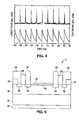
- FIG. 4 illustrates a verification of the working principle of the device demonstrated with a laser produced plasma.
- the upper curve shows the signal generated by a photodiode illuminated by the laser radiation, the lower signal was generated by the setup shown in FIG. 1 .
- the two signal lengths are different due to different rise times of the used photodiodes.
- the EUV source was a laser produced plasma.
- the two signals show the laser pulses detected by a photodiode (top signal) and the EUV signal detected with a device shown in FIG. 1 .
- Another advantageous feature of the proposed device is the use of a focussing multilayer mirror with a curved surface. This can increase the photon flux on the detector and the sensitivity of the monitor setup.
- a beam parameter monitoring unit for coupling with an EUV source that produces an output beam having a wavelength around 11-15 nm.
- the monitoring unit schematically illustrated at FIGS. 5-8 includes a beam splitter, a detector and a beam path enclosure.
- the beam splitter is disposed to separate the output beam into a first component and a second component, wherein the first component is used for processing a workpiece.
- the detector includes a platinum silicide window or it otherwise comprises a Si dead region diode, PtSi, and particularly PtSi-nSi, for measuring at least one optical parameter of the second component of the output beam after the beam splitter.
- the presence of the platinum silicide reduces EUV radiation exposure induced instability of the detector.
- the beam path enclosure contains the beam splitter and has an interior prepared such that an optical path of the second component of the output beam through the enclosure from the laser resonator to the detector via the beam splitter is substantially free of EUV photoabsorbing species so that the second component reaches the detector without substantial attenuation from the photoabsorbing species.
- FIG. 5 shows an embodiment of a detector 3 for use in a detector housing 2 coupled with a beam path enclosure 1 as described below with respect to FIGS. 6-8 .
- the particular detector 3 shown in FIG. 5 is manufactured by International Radiation Detectors, Inc. and further information may be found at www.ird-inc.com, which information contained at that web site is hereby incorporated by reference. It is recognized herein that the detector shown at FIG. 5 has been particularly configured for use with VUV exposure radiation and that the detector shown at FIG. 5 may be modified according to its use with EUV exposure wavelengths.
- the detector 3 shown includes a platinum silicide (PtSi) window 38 for reducing EUV radiation exposure induced instability of the detector 3 . More than one PtSi layer may be included in the detector design. The platinum silicide layer may be located in another location, such as beneath one or more other material layers of the device.
- the detector 3 also may include a defect free n-type region 40 beneath the PtSi window 38 and above an epitaxial p-type region which itself lies above a p+ substrate 44 over a chromium gold base layer 46 .
- the detector 3 shown also may have four aluminum contacts 48 and four insulating field oxide regions 50 . A pair of p+ regions and a pair of n+ regions are also shown implanted into the epitaxial layer 42 .
- the PtSi reduces EUV radiation exposure induced instability of the detector 3 .
- the PtSi may be used in combination with other materials to form a hybrid layer.
- the PtSi may have substitutional or inter-dispersed species doped therein, or PtSi itself may be doped into another material-type layer.
- Several PtSi layers may be included, wherein the PtSi layers may have other material layers therebetween.
- PtSi may be used in a detector that is protected within an enclosure for delivering EUV radiation, particularly around 11-15 nm, as is preferably emitted by an extreme ultraviolet radiation source, and that although an embodiment is shown at FIG. 5 as a detailed schematic of a detector 3 of FIGS. 6-8 , below, the detector 3 of FIGS. 6-8 preferably includes PtSi in any of a variety of forms and locations within the detector 3 as may be understood by those skilled in the art.
- the invention provides a detector for a monitoring an output beam parameter of an extreme ultraviolet radiation source emitting radiation around 11-15 nm.
- Preferred embodiments preferably exhibit little or no degradation of spectral sensitivity even after high exposure dosage.
- the preferred embodiments include EUV-photodetectors which are very stable under strong 11-15 nm exposure preferably under inert gas purged or evacuated illumination conditions.
- the preferred embodiments include an evacuatable or purgeable vacuum tight energy monitor housing which contains an advantageously stable EUV-photodiode detector. Radiation attenuators, apertures, EUV-light scattering plates, electrical pass through means, purge gas inlet and/or means of flowing purging gas through the exposed detector housing or for evacuating the housing may also be included.
- FIG. 6 schematically shows a beam splitting enclosure including an energy detector 3 within an energy detector housing 2 and beam splitting optics 4 a , 4 b within a beam path enclosure preferably connected through a vacuum seal to the detector enclosure 2 .
- FIG. 6 shows in detail a beam path enclosure 1 containing the beam splitting optics 4 a , 4 b .
- the enclosure 1 may have an interior prepared such that an optical path of a incoming beam 7 a and a split off beam portion 7 c of the beam 7 a through the enclosure 1 from an EUV source (not shown in FIG. 6 ) to a detector housing 2 containing the detector 3 is substantially free of EUV absorbing species so that the beam portion 7 c can reach the detector without substantial attenuation due to the presence of EUV absorbing species.
- the incoming beam 7 a is preferably coming from an EUV radiation source (not shown in FIG. 6 ).
- the enclosure 1 is either connected directly to the output of the EUV source, or at least a beam path from the output to a window 9 of the enclosure is substantially free of EUV absorbing species such as having a flow of inert gas or substantial vacuum continuously present in the path of the beam 7 a.
- the beam 7 b is shown passing through the beam splitter 4 a and exiting from the enclosure 1 .
- Another enclosure of a beam path that leads to an application process may be connected directly to the enclosure, or at least the beam path is free of EUV absorbing species, such as described above with respect to the incoming beam.
- the beam 7 a may alternatively be previously split off from a beam that is transmitted to an application process, or the beam that is used at the application process may be the output from the EUV source, or vice-versa with respect to these two beams.
- the beam 7 a is shown incident at a beam splitter 4 a .
- the beam splitter 4 a is preferably an uncoated EUV transmissive plate such as of a material known to those skilled in the art.
- the beam 7 c is then reflected from an EUV mirror 4 b through optics 5 and into the detector enclosure 2 and is incident on the detector 3 .
- the energy monitor unit includes a beam separation box containing beam splitting optics 4 a , 4 b and the EUV detector housing 2 which contains a preferred EUV-photodetector 3 , as described in more detail elsewhere herein.
- the EUV detector housing 2 is directly connected to the beam path enclosure 1 by a suitable vacuum fitting, preferably a DN40 flange (not shown in FIG. 6 , but see flange 16 at FIG. 7 ).
- Both housings 1 and 2 are preferably vacuum tight and are purged by suitable purge gases, or are evacuated, such as a noble gas such as Ar or another inert gas that does not significantly absorb EUV radiation, e.g., around 11-15 nm.
- This preferred arrangement advantageously prevents absorption of the EUV radiation which is emitted by the EUV source, and enters the beam enclosure 1 from the left in FIG. 6 via a purged or evacuated beam line directly connected to the output of the EUV source (not shown in FIG. 6 ), or otherwise as discussed herein.
- the beam separation box including the enclosure 1 contains suitable optics to split a certain beam portion 7 c (about 1% to 15%) of the main beam 7 a , and redirect the beam portion 7 c into the detector housing 2 , and those optics may be alternatively to those described above, such as are described at the '552 and/or '952 applications, mentioned above.
- Such means may include an aperture disposed at or near position 8 of FIG. 6 .
- the beam splitting optics 4 a , 4 b within the enclosure 1 of the beam separation box may include a blank uncoated beam splitter 4 a disposed in the path of the main beam line 7 a and a highly reflective (HR) mirror for EUV radiation 4 b as an additional beam steering mirror.
- HR highly reflective
- This configuration is advantageously inexpensive to manufacture and prevents problems associated with coating damage due to exposure to the high power main beam 7 a .
- the beam splitter 4 a may, however, include one or more coatings.
- a beam splitter is not used. Instead, a first beam is output from an EUV source and a second beam is output from the EUV source already separate from each other.
- the second beam may be output from another location of the EUV source, such that the first beam is output at one end of the EUV source chamber and the second beam is output at the other end of the EUV source chamber.
- the output location of the EUV source may be configured to separate the two beam components. Therefore, including a beam splitter 4 a , or other optic having a partially reflecting surface for separating a single output beam into two components such that one component is used to process a workpiece and the other incident at an EUV detector 3 is merely preferred and not necessary, as understood from the above.
- the component measured at the detector 3 has at least one parameter such as energy, wavelength, bandwidth, spatial or temporal beam profile, divergence, spatial or temporal coherence, etc. that it is desired to be measured that has a known relationship to the same parameter in the other component that is used for processing the workpiece.
- FIG. 7 shows a schematic view of the detector housing 2 of FIG. 6 in more detail.
- the detector housing 2 includes a gas purge inlet 12 , and a signal cable connector 14 which is preferably a BNC connector, as shown, and may be another signal cable connector as understood by those skilled in the art, for transmitting electrical signals between the detector 3 and monitoring equipment such as a processor or viewing scope (not shown).
- the signal cable connector 14 is preferably mounted to the housing 2 by a vacuum tight seal.
- the detector housing 2 preferably includes one or more apertures and slits for insertion of an EUV attenuator 18 , one or more scattering plates 20 and the EUV-detector itself 3 .
- the detector housing 2 also preferably has a flange 16 , such as preferably a DN40 flange, for vacuum tight coupling to the enclosure 1 of FIG. 6 . Additionally the detector housing 2 is preferably covered by an electrically conducting shield (not shown), which could be a fine wire mesh or other electrical or magnetic shielding as understood by those skilled in the art, to prevent EMV noise from penetrating into the detector housing 2 . Preferably, the detector housing 2 is vacuum tight at all connections and contains multiple purge gas slits including gas inlet 12 to ensure a substantially evacuated condition or an even and continuously flowing purge gas throughput into all areas of the detector housing 2 .
- the detector housing 2 may be advantageously quickly evacuated and backfilled or purged with an inert gas without accumulation of contaminants or EUV photoabsorptive species of gas which could otherwise produce errors in monitoring a beam parameter by detecting the small amount of EUV radiation 7 c which is received at the detector 3 (typically about 1% to 0.001% of the radiation density of the main part of the beam 7 a ).
- the detector 3 receives a beam portion 7 c which enters a front portion 21 of the detector housing 2 where the flange 16 connects sealably to the enclosure 1 of FIG. 7 .
- the beam traverses the attenuator 18 and scattering plates 20 and preferably one or more apertures (not shown) prior to impinging upon the detector 3 .
- the signal cable connector 14 is located in a back portion 22 a of the detector housing 2 .
- FIG. 8 schematically shows a detailed view of a modified embodiment of the back portion 22 b of a vacuum tight detector, which performs a same function as the detector housing 2 of FIG. 8 , and which shows the detector 3 disposed within the back portion 22 b .
- the beam 7 c is then incident at the detector 3 through an optical opening between the front portion 21 (not shown, but see FIG. 8 ) and the back portion 22 b .
- the signal cable connector plug 24 has two O-ring seals 26 , 28 between three housing sections 30 , 32 , 34 to the back portion of detector housing 22 b , making it vacuum tight.
- FIG. 9 schematically shows an EUV generating source in cross section in accord with an exemplary embodiment.
- the features described above and below with reference to FIGS. 1-8 and 10 - 13 may be implemented in any of a wide variety of EUV sources, and many of those alternative sources may be understood by reviewing the reference incorporated by reference into this application and also as may be understood by those skilled in the art.
- Many components of the exemplary EUV source shown in FIG. 9 may be understood from the description at U.S. Pat. No. 5,504,795 which is hereby incorporated by reference.
- the EUV source includes a pinch chamber 10 having a pinch region 12 defining a central axis 14 at the end of which is an EUV photon transmitting window 18 .
- a dielectric liner 24 surrounds preferably the pinch region 12 .
- a gas supply inlet 20 and an outlet 22 controllably supply active and diluent gases to the pinch region 12 .
- the outlet 22 is connected to a vacuum pump 23 .
- Other gas supply systems are possible such as may be borrowed and/or modified from excimer laser technology (see U.S. Pat. Nos. 4,977,573 and 6,212,214, and U.S. patent application Ser. Nos. 09/447,882 and 09/453,670, each of which is assigned to the same assignee as the present application, and U.S. Pat. Nos. 5,978,406 and 5,377,215, all of which are hereby incorporated by reference).
- the gas may be circulated and electrostatic and/or cryogenic purification filters may be inserted into the gas loop (see U.S. Pat. Nos. 4,534,034, 5,136,605 and 5,430,752, each of which is hereby incorporated by reference).
- a heat exchanger may also be provided in the gas loop (see the '670 application, mentioned above and U.S. Pat. No. 5,763,930, which is hereby incorporated by reference).
- the gas mixture includes an x-radiating gas such as xenon, krypton, argon, neon, oxygen or lithium.
- the gas mixture also preferably includes a low atomic number diluent gas such as helium, hydrogen, deuterium, and possibly nitrogen.
- xenon (11-15 nm), lithium (13.4 nm) and/or oxygen (13.0 nm), and preferably a buffer gas such as helium, are used.
- a preionization electrode 26 is connected to a preionization unit 27 for preionizing the gas in the pinch region 12 .
- preionization unit types are possible such as e-beam, conical pinch discharge and RF preionization (see the '795 patent, mentioned above, U.S. patent application Ser. No. 09/693,490, which is assigned to the same assignee as the present application, and C. Stallings, et al., Imploding Argon Plasma Experiments, Appl. Phys. Lett. 35 (7), Oct. 1, 1979, which are hereby incorporated by reference).
- Some known laser preionization systems may be modified to provide preionization for the EUV source, as well (see U.S. Pat. Nos.
- the preionization unit 27 and electrode 26 preionizes the pinch plasma in a symmetrical shell around the central axis 14 , as shown, prior to the application of the main pulse to the main electrodes 30 and 32 .
- the preferred main electrodes 30 , 32 are as shown in FIG. 9 .
- the anode 30 and the cathode 32 are shown located at opposite ends of the pinch region 12 .
- Many other anode-cathode configurations are possible (see U.S. Pat. Nos. 3,961,197, 5,763,930, 4,504,964 and 4,635,282, each of which is hereby incorporated by reference).
- a power supply circuit 36 including a voltage source 37 , a switch 38 and capacitor 39 connected to electrodes 30 , 32 generates electrical pulses that produce high electric fields in the pinch region which in turn create azimuthal magnetic fields causing the preionized plasma to rapidly collapse to the central axis 14 to produce an EUV beam output along the central axis 14 .
- Many power supply circuits are possible (see U.S. Pat. No. 5,142,166 which is hereby incorporated by reference).
- the anode 30 and cathode 32 are separated by an insulator 40 .
- a prepulse may be generated, as well.
- the prepulse occurs just prior to the main pulse and after the plasma is substantially preionized by the preionization unit 27 and electrode 26 .
- the prepulse is a relatively low energy discharge provided by the main electrodes 30 , 32 .
- the prepulse creates more homogeneous conditions in the already preionized plasma preventing electrode burnout at hotspots from arcing due to the high voltage, fast rise time of the main pulse.
- a prepulse circuit is described at Giordano et al., referred to and incorporated by reference, below, and may be modified to suit the EUV source of the preferred embodiment.
- a first is a clipping aperture 300 which is spaced a proximate distance from the pinch region 12 .
- the clipping aperture 300 may be formed as shown or may be offset at an angle such as is described at U.S. Pat. No. 5,161,238 which is assigned to the same assignee as the present application and is hereby incorporated by reference.
- the clipping aperture 300 comprises a material exhibiting a high thermal stability. That is, the clipping aperture preferably has a high thermal conductivity and a low coefficient of thermal expansion.
- the clipping aperture preferably comprises a ceramic material such as Al 2 O 3 , sapphire or alumina.
- the clipping aperture is positioned close to the pinch region, but not too close to the pinch region 12 that thermal effects degrade its performance.
- the clipping aperture 300 blocks acoustic waves and particulates travelling with the acoustic waves from following the beam on the remainder of its journey through the pinch chamber 10 .
- the aperture is further preferably configured to reflect and/or absorb the acoustic waves so that they do not reflect back into the pinch region 12 .
- the size of the clipping aperture 300 is selected to match the divergence of the beam.
- a set of baffles 400 is provided after the clipping aperture.
- the baffles 400 may be configured similar to those described at U.S. Pat. No. 5,027,366, which is hereby incorporated by reference.
- the baffles 400 serve to diffuse the effect of acoustic waves emanating from the pinch region such as the flow of gases and contaminant particulates travelling with the acoustic waves, as well as to prevent reflections back into the pinch region.
- the baffles 400 preferably absorb such disturbances.
- An ionizing unit 500 is shown located after the baffles 400 .
- the ionizing unit 500 may be located before the baffles 400 or between two sets of baffles 400 .
- the ionizing unit preferably emits UV radiation.
- the ionizing unit 500 is preferably corona type, such as corona wires or electrodes.
- the UV light from the ionizer unit 500 ionizes dust particles that tend to travel along with the beam.
- An electrostatic particle filter 600 a , 600 b is provided for collecting the charged dust particles resulting in a cleaner beam path. Fewer of these contaminants are deposited on the window 18 and elsewhere in the chamber 14 . Also, the ionizer/precipitator arrangement reduces reflections from the particulates by the EUV beam, as well as other disturbances to the beam.
- the clipping aperture and set of baffles reduce the influence of acoustic waves emanating from the pinch region 12 .
- the clipping aperture also matches the divergence of the beam.
- the prepulse generated prior to the main pulse serves to homogenize the plasma shell to reduce the probability that arcing will degrade the pinch symmetry and the resulting EUV beam and that hotspots due to the arcing will deteriorate the electrodes 30 , 32 .
- the ionizer 500 and precipitator 600 a , 600 b serve to remove particulates from the beam path preventing adverse effects on the beam and components such as the beam exit window 18 of the chamber 10 where the particulates may become otherwise deposited.
- FIGS. 10-13 schematically illustrate additional embodiments and/or alternative features that may be combined with the above-described preferred embodiments.
- the embodiments of FIGS. 10-13 relate generally to use of a multilayer mirror to increase the usable angle in gas discharge based photon Sources (e.g., Z-pinch (FIG. 10 ), HCT-pinch (FIG. 11 ), capillary discharge ( FIG. 12 ) and plasmafokus or plasma focus (FIG. 13 )).
- the mirror could be flat or may have a curved shape with imaging properties, preferably installed in a gas discharge EUV photon source.
- the output power of gas discharge based photon sources in the extreme ultraviolet and soft x-ray spectral range may be increased using a mirror according to these alternative embodiments. Another advantage is that this effect of increased power may be obtained while leaving other conditions unaltered.
- the usable angle of a gas discharge based photon source is often limited by the electrodes of the discharge system itself. Furthermore, it is often difficult to increase the aperture.
- the electrical input power may be increased. Under the same discharge conditions, this leads to higher power in the electrode system correlated with higher temperatures.
- the preferred embodiments which include the multilayer mirrors increases the output power of such a source leaving other parameters such as input power unaltered.
- Gas discharge based photon sources generate a hot dense plasma, which emits radiation into a solid angle of 4 ⁇ sr. Radiation emitted in an other direction than the open solid angle of the electrode system, which is defined by the aperture and its distance to the plasma, is absorbed within the source and cannot be used.
- the described mirror reflects parts of this radiation and guides it through the accessible aperture.
- the mirror is preferably a multilayer mirror, which is adapted to the wavelength of the radiation (preferably between 11 nm and 15 nm) and the angle of incidence. This angle can vary laterally on the surface of the mirror and gradient multilayers may be used.
- the generated plasma generally has the shape of a small column (e.g., less than 1 mm, such as around 0.53 mm).
- the optical thickness along the symmetry axis for the emitted radiation is typically high.
- the reflected radiation does not pass through the plasma itself due to the opaque nature of the plasma.
- the shape of the mirror is adapted to the emission characteristic of the source.
- the imaging properties of the mirror are such that a substantial amount or even most of the reflected radiation is guided apart from the plasma column to the open aperture of the electrode system.
- a flat mirror will improve the output power of the source, and may be useful with some configurations.
- an elliptical mirror with adapted focal length will focus the radiation in front of the output aperture, and a hyperbolic mirror will generate almost parallel radiation. This degree of freedom of changing the mirror shape to adapt the emission properties of the source to the optical system of the application may be advantageously used.
- the improvement of the output power of the sources, e.g., those illustrated at FIGS. 10-13 , by consideration of the geometry of the electrode systems is described in Table 1 below.
- the solid angle (in steradians or sr.) of the emitted radiation is understood from recent publications.
- 10 is the intensity emitted isotropically by the plasma into a solid angle of 4 ⁇ sr.
- the output is calculated out of these two values.
- the estimated mirror acceptance angle is the upper value, limited by the electrode systems.
- the reflectivity of the mirrors is set to 70% close to the best demonstrated values from literature for normal incidence radiation.
- the increase of output is calculated by multiplication of the solid angle of the mirror and its reflectivity.
- the “improvement” value in table 1 is the quotient of the increase of output and the initial output of each source.
- the highest increase of the output power is expected for the z-pinch and HCT-pinch geometries illustrated at FIGS. 10 and 11 , respectively.
- the usable angles of capillary discharges and plasmafocus devices, illustrated at FIGS. 12 and 13 , respectively, initially are very high such that the expected improvement according to these preferred embodiments is smaller in relation to the output power than for the z-pinch and HCT-pinch arrangements, as shown in Table 1.
- the mirrors may be formed from silicon/beryllium and/or molybdenum/silicon multilayers.
Abstract
Description
| TABLE 1 | ||||
| Source/ | Capillary | |||
| Parameter | z-pinch | HCT-pinch | discharge | Plasmafocus |
| solid angle | 0.3 | 1 | πsr | 2 πsr | |
| Output | 0.3/4 | 1/4 π IO | π/4 | 2 π/4 π IO | |
| IO | |||||
| Estimated | 1 | 1 sr | 0.3 | 1 sr | |
| mirror | |||||
| acceptance | |||||
| angle | |||||
| Multilayer | 70% | 70% | 70% | 70% | |
| reflectivity | |||||
| Increase of | 1/4 π × | 1/4 π × | 0.3/4 π × | 1/4 π × | |
| output by | .07 IO | .07 IO | .07 IO | .07 IO | |
| mirrow | |||||
| Increase output | 5.6% | 5.6% | 1.7% | 5.6% | |
| in % of IO | |||||
| Expected | 230% | 70% | 6.8% | 11.2% | |
| improvement | |||||
The preferred mirrors are treated by heat and/or ion bombardement from the plasma of the devices shown in
Claims (18)
Priority Applications (1)
| Application Number | Priority Date | Filing Date | Title |
|---|---|---|---|
| US10/218,690 US6998620B2 (en) | 2001-08-13 | 2002-08-12 | Stable energy detector for extreme ultraviolet radiation detection |
Applications Claiming Priority (2)
| Application Number | Priority Date | Filing Date | Title |
|---|---|---|---|
| US31227701P | 2001-08-13 | 2001-08-13 | |
| US10/218,690 US6998620B2 (en) | 2001-08-13 | 2002-08-12 | Stable energy detector for extreme ultraviolet radiation detection |
Publications (2)
| Publication Number | Publication Date |
|---|---|
| US20030058429A1 US20030058429A1 (en) | 2003-03-27 |
| US6998620B2 true US6998620B2 (en) | 2006-02-14 |
Family
ID=23210700
Family Applications (1)
| Application Number | Title | Priority Date | Filing Date |
|---|---|---|---|
| US10/218,690 Expired - Lifetime US6998620B2 (en) | 2001-08-13 | 2002-08-12 | Stable energy detector for extreme ultraviolet radiation detection |
Country Status (4)
| Country | Link |
|---|---|
| US (1) | US6998620B2 (en) |
| EP (1) | EP1417543A1 (en) |
| JP (1) | JP4445258B2 (en) |
| WO (1) | WO2003017005A1 (en) |
Cited By (7)
| Publication number | Priority date | Publication date | Assignee | Title |
|---|---|---|---|---|
| US20090046273A1 (en) * | 2007-08-16 | 2009-02-19 | Vivek Bakshi | Systems and Methods for Monitoring and Controlling the Operation of Extreme Ultraviolet (EUV) Light Sources Used in Semiconductor Fabrication |
| US20100258749A1 (en) * | 2009-04-09 | 2010-10-14 | Partlo William N | System, method and apparatus for laser produced plasma extreme ultraviolet chamber with hot walls and cold collector mirror |
| US20110192985A1 (en) * | 2007-12-20 | 2011-08-11 | Bowering Norbert R | Euv light source components and methods for producing, using and refurbishing same |
| CN102680120A (en) * | 2012-05-24 | 2012-09-19 | 哈尔滨工业大学 | Detection system for extreme ultraviolet lithography light source in Xe10+ ionic condition |
| US20130032700A1 (en) * | 2011-08-04 | 2013-02-07 | Lockheed Martin Corporation | Laser drawn electronics |
| US20140314210A1 (en) * | 2013-04-19 | 2014-10-23 | Raytheon Company | X-ray cells and other components having gas cells with thermally-induced density gradients |
| US10069273B1 (en) | 2017-03-02 | 2018-09-04 | Coherent Lasersystems Gmbh & Co. Kg | Lasing-gas mixture for excimer laser |
Families Citing this family (26)
| Publication number | Priority date | Publication date | Assignee | Title |
|---|---|---|---|---|
| TW380040B (en) * | 1995-06-07 | 2000-01-21 | Pillsbury Co | Leavened dough compositions and process of increasing specific volume in a baked product |
| KR20020030736A (en) * | 2000-01-25 | 2002-04-25 | 추후제출 | Energy monitor for molecular fluorine laser |
| US7230964B2 (en) * | 2001-04-09 | 2007-06-12 | Cymer, Inc. | Lithography laser with beam delivery and beam pointing control |
| US20050259709A1 (en) * | 2002-05-07 | 2005-11-24 | Cymer, Inc. | Systems and methods for implementing an interaction between a laser shaped as a line beam and a film deposited on a substrate |
| US6710351B2 (en) * | 2001-09-18 | 2004-03-23 | Euv, Llc | EUV mirror based absolute incident flux detector |
| DE10204994B4 (en) * | 2002-02-05 | 2006-11-09 | Xtreme Technologies Gmbh | Arrangement for monitoring the energy emission of an EUV radiation source |
| DE10219805B4 (en) * | 2002-04-30 | 2013-03-14 | Xtreme Technologies Gmbh | A method for stabilizing the radiant power of a pumped gas-generated plasma source |
| JP2006503419A (en) * | 2002-10-11 | 2006-01-26 | インフィネオン テクノロジーズ アクチエンゲゼルシャフト | Irradiation device for inspecting an object covered with a photosensitive resist |
| US6781135B2 (en) * | 2002-11-21 | 2004-08-24 | Euv, Llc | Universal EUV in-band intensity detector |
| JP2004303760A (en) * | 2003-03-28 | 2004-10-28 | Canon Inc | Device and method for measuring euv light intensity distribution |
| US7277188B2 (en) * | 2003-04-29 | 2007-10-02 | Cymer, Inc. | Systems and methods for implementing an interaction between a laser shaped as a line beam and a film deposited on a substrate |
| JP4262032B2 (en) * | 2003-08-25 | 2009-05-13 | キヤノン株式会社 | EUV light source spectrum measurement device |
| FR2861184B1 (en) * | 2003-10-17 | 2006-01-13 | Eppra | METHOD FOR GENERATING DESIRED WAVE LENGTH RADIATION, AND DEVICE THEREOF |
| US7196342B2 (en) * | 2004-03-10 | 2007-03-27 | Cymer, Inc. | Systems and methods for reducing the influence of plasma-generated debris on the internal components of an EUV light source |
| US7449703B2 (en) * | 2005-02-25 | 2008-11-11 | Cymer, Inc. | Method and apparatus for EUV plasma source target delivery target material handling |
| US7679029B2 (en) * | 2005-10-28 | 2010-03-16 | Cymer, Inc. | Systems and methods to shape laser light as a line beam for interaction with a substrate having surface variations |
| US7317179B2 (en) * | 2005-10-28 | 2008-01-08 | Cymer, Inc. | Systems and methods to shape laser light as a homogeneous line beam for interaction with a film deposited on a substrate |
| US7329876B2 (en) | 2006-01-26 | 2008-02-12 | Xtreme Technologies Gmbh | Narrow-band transmission filter for EUV radiation |
| US7760341B2 (en) * | 2007-09-04 | 2010-07-20 | Sematech, Inc. | Systems and methods for in-situ reflectivity degradation monitoring of optical collectors used in extreme ultraviolet (EUV) lithography processes |
| DE102008000957A1 (en) * | 2008-04-03 | 2009-10-08 | Carl Zeiss Smt Ag | Protection module and EUV lithography device with protection module |
| JP5534910B2 (en) * | 2009-04-23 | 2014-07-02 | ギガフォトン株式会社 | Extreme ultraviolet light source device |
| CN102494765A (en) * | 2011-11-21 | 2012-06-13 | 哈尔滨工业大学 | Extreme ultraviolet light detection system capable of real-timely acquiring extreme ultraviolet light radiation characteristic |
| CN104204951B (en) * | 2012-03-20 | 2017-03-01 | Asml荷兰有限公司 | Lithographic equipment, sensor and method |
| DE102014223411A1 (en) * | 2014-11-17 | 2016-05-19 | Carl Zeiss Smt Gmbh | Arrangement and method for measuring the intensity of electromagnetic radiation in an optical system |
| WO2017187571A1 (en) * | 2016-04-27 | 2017-11-02 | ギガフォトン株式会社 | Extreme ultraviolet light sensor unit and extreme ultraviolet light generation device |
| CN111189536A (en) * | 2019-12-30 | 2020-05-22 | 中国科学院长春光学精密机械与物理研究所 | Space extreme ultraviolet photometer |
Citations (119)
| Publication number | Priority date | Publication date | Assignee | Title |
|---|---|---|---|---|
| US4009933A (en) | 1975-05-07 | 1977-03-01 | Rca Corporation | Polarization-selective laser mirror |
| US4240044A (en) | 1979-07-16 | 1980-12-16 | Gte Products Corporation | Pulsed laser electrode assembly |
| US4380079A (en) | 1980-09-12 | 1983-04-12 | Northrop Corp. | Gas laser preionization device |
| US4393505A (en) | 1978-07-24 | 1983-07-12 | Gte Sylvania Incorporated | Gas discharge laser having a buffer gas of neon |
| US4399540A (en) | 1979-05-10 | 1983-08-16 | Lamba Physik Gesellschaft Zur Herstellung Von Lasern Mbh & Co. Kg | Tunable laser oscillator |
| US4611270A (en) | 1983-09-16 | 1986-09-09 | Questek Incorporated | Method and means of controlling the output of a pulsed laser |
| US4616908A (en) | 1984-07-19 | 1986-10-14 | Gca Corporation | Microlithographic system |
| US4674099A (en) | 1984-05-01 | 1987-06-16 | Turner Robert E | Recycling of gases for an excimer laser |
| US4686682A (en) | 1984-10-09 | 1987-08-11 | Mitsubishi Denki Kabushiki Kaisha | Discharge excitation type short pulse laser device |
| US4691322A (en) | 1985-01-22 | 1987-09-01 | Kabushiki Kaisha Komatsu Seisakusho | Gas laser device |
| US4719637A (en) | 1985-03-13 | 1988-01-12 | Enea-Comitato Nazionale Per La Ricerca E Lo Sviluppo Dell'energia Nucleare E Delle Energie Alternative | Laser doped with tripropylamine |
| US4829536A (en) | 1986-06-09 | 1989-05-09 | Kabushiki Kaisha Komatsu Seisakusho | Multi-mode narrow-band oscillation excimer laser |
| US4835580A (en) * | 1987-04-30 | 1989-05-30 | Texas Instruments Incorporated | Schottky barrier diode and method |
| US4856018A (en) | 1986-01-22 | 1989-08-08 | Kabushiki Kaisha Komatsu Seisakusho | Light source for reduced projection |
| US4860300A (en) | 1987-06-03 | 1989-08-22 | Lambda Physik Forschungs- Und Entwicklungsgesellschaft Mb | Electrode for pulsed gas lasers |
| US4891818A (en) | 1987-08-31 | 1990-01-02 | Acculase, Inc. | Rare gas-halogen excimer laser |
| US4905243A (en) | 1987-12-28 | 1990-02-27 | Lambda Physik Forschungs-Und Entwicklungs-Gmbh | Method and apparatus for stabilizing the frequency of a laser beam |
| US4926428A (en) | 1987-08-31 | 1990-05-15 | Kabushiki Kaisha Komatsu Seisakucho | Method and apparatus for sensing the wavelength of a laser beam |
| US4953174A (en) | 1989-10-23 | 1990-08-28 | Hughes Aircraft Company | Preionization electrode for pulsed gas laser |
| US4975919A (en) | 1987-03-19 | 1990-12-04 | Kabushiki Kaisha Komatsu Seisakusho | Laser wavelength control apparatus |
| US5001721A (en) | 1989-06-16 | 1991-03-19 | Lambda Physik Forschungs- Und Entwicklungsgesellschaft Mbh | Apparatus for purifying laser gas |
| US5005181A (en) | 1988-10-20 | 1991-04-02 | Mitsubishi Denki K.K. | Method for controlling gas in halogen gas laser and device therefor |
| US5025445A (en) | 1989-11-22 | 1991-06-18 | Cymer Laser Technologies | System for, and method of, regulating the wavelength of a light beam |
| US5051558A (en) | 1989-03-20 | 1991-09-24 | Sukhman Yefim P | Laser material processing apparatus and method therefore |
| US5081635A (en) | 1987-08-25 | 1992-01-14 | Kabushiki Kaisha Komatsu Seisakusho | Apparatus for controlling output from an excimer laser device |
| US5095492A (en) | 1990-07-17 | 1992-03-10 | Cymer Laser Technologies | Spectral narrowing technique |
| US5099491A (en) | 1990-11-26 | 1992-03-24 | American Laser Corporation | Laser gas replenishment system |
| US5111473A (en) | 1990-01-25 | 1992-05-05 | Lambda Physik Forschungs- Und Entwicklungsgesellschaft Mbh | Laser gas purifying apparatus |
| US5136605A (en) | 1990-03-27 | 1992-08-04 | Lambda Physik Gesellschaft Zur Herstellung Von Lasern Mbh | Apparatus for purifying laser gas |
| US5140600A (en) | 1990-11-28 | 1992-08-18 | Lambda Physik Gesellschaft Zur Herstellung Von Lasern Mbh | Method of controlling the total energy amount of a plurality of laser pulses |
| US5142543A (en) | 1988-01-27 | 1992-08-25 | Kabushiki Kaisha Komatsu Seisakusho | Method and system for controlling narrow-band oscillation excimer laser |
| US5150370A (en) | 1989-06-14 | 1992-09-22 | Matsushita Electric Industrial Co., Ltd. | Narrow-band laser apparatus |
| US5221823A (en) | 1991-07-03 | 1993-06-22 | Mitsubishi Denki K.K. | Laser machining apparatus for welding and cutting |
| US5226050A (en) | 1990-01-25 | 1993-07-06 | Lambda Physik Forschungs - Und Entwicklungsgesellschaft - Gmbh | Small line width tunable laser |
| US5243614A (en) | 1990-11-28 | 1993-09-07 | Mitsubishi Denki Kabushiki Kaisha | Wavelength stabilizer for narrow bandwidth laser |
| US5247535A (en) | 1991-03-15 | 1993-09-21 | Lambda Physik Forschungsgesellschaft Mbh | Apparatus for preionization of gas in a pulsed gas laser |
| US5247534A (en) | 1991-04-23 | 1993-09-21 | Lambda Physik Forschungsgesellschaft Mbh | Pulsed gas-discharge laser |
| US5247531A (en) | 1991-03-15 | 1993-09-21 | Lambda Physik Forschungsgesellschaft Mbh | Apparatus for preionizing apulsed gas laser |
| US5307364A (en) | 1993-05-24 | 1994-04-26 | Spectra Gases, Inc. | Addition of oxygen to a gas mix for use in an excimer laser |
| US5311565A (en) * | 1991-05-31 | 1994-05-10 | Olympus Optical Co., Ltd. | Soft X-ray microscope |
| US5331456A (en) * | 1991-12-09 | 1994-07-19 | Olympus Optical Co., Ltd. | Radiation microscope |
| US5337330A (en) | 1992-10-09 | 1994-08-09 | Cymer Laser Technologies | Pre-ionizer for a laser |
| US5396514A (en) | 1992-03-04 | 1995-03-07 | Lamba Physik Gesellschaft Zur Herstelling Von Lasern Mbh | Excimer laser comprising a gas reservoir and a collecting receptacle and a method of refilling the gas reservoir of the laser with halogen gas |
| US5404366A (en) | 1989-07-14 | 1995-04-04 | Kabushiki Kaisha Komatsu Seisakusho | Narrow band excimer laser and wavelength detecting apparatus |
| US5405207A (en) | 1993-07-23 | 1995-04-11 | Zubli; Leslie A. | Voice pen for generating audible messages |
| US5434901A (en) * | 1992-12-07 | 1995-07-18 | Olympus Optical Co., Ltd. | Soft X-ray microscope |
| US5440578A (en) | 1993-07-16 | 1995-08-08 | Cymer Laser Technologies | Gas replenishment method and apparatus for excimer lasers |
| US5450463A (en) * | 1992-12-25 | 1995-09-12 | Olympus Optical Co., Ltd. | X-ray microscope |
| US5463650A (en) | 1992-07-17 | 1995-10-31 | Kabushiki Kaisha Komatsu Seisakusho | Apparatus for controlling output of an excimer laser device |
| US5504795A (en) | 1995-02-06 | 1996-04-02 | Plex Corporation | Plasma X-ray source |
| US5533083A (en) * | 1992-09-10 | 1996-07-02 | Olympus Optical Co., Ltd. | Vacuum optical system |
| US5535233A (en) | 1992-08-28 | 1996-07-09 | Kabushiki Kaisha Komatsu Seisakusho | Laser device |
| US5534034A (en) | 1990-07-13 | 1996-07-09 | Caspers; Carl A. | Prosthetic polyurethane liner and sleeve for amputees |
| US5559584A (en) | 1993-03-08 | 1996-09-24 | Nikon Corporation | Exposure apparatus |
| US5559816A (en) | 1994-10-26 | 1996-09-24 | Lambda Physik Gesellschaft Zur Herstellung Von Lasern Mbh | Narrow-band laser apparatus |
| US5596596A (en) | 1989-05-18 | 1997-01-21 | Kabushiki Kaisha Komatsu Seisakusho | Narrow band excimer laser |
| US5598300A (en) | 1995-06-05 | 1997-01-28 | Board Of Regents, The University Of Texas System | Efficient bandpass reflection and transmission filters with low sidebands based on guided-mode resonance effects |
| US5606586A (en) * | 1992-09-14 | 1997-02-25 | Canon Kabushiki Kaisha | X-ray exposure method and apparatus and device manufacturing method |
| US5652681A (en) | 1992-12-18 | 1997-07-29 | Hughes Electronics | Grism (grating-prism combination) |
| US5659419A (en) | 1994-08-23 | 1997-08-19 | Lambda Physik Gesellschaft Zur Herstellung Von Lasern Mbh | Tunable narrowband optical parametrical oscillator |
| US5659531A (en) | 1993-02-16 | 1997-08-19 | Nec Corporation | Optical head device and birefringent diffraction grating polarizer and polarizing hologram element used therein |
| US5663973A (en) | 1996-05-14 | 1997-09-02 | Lambda Physik Gesellschaft Zur Herstellung Von Lasern Mbh | Tunable narrowband source of a coherent radiation |
| US5684822A (en) | 1994-11-17 | 1997-11-04 | Cymer, Inc. | Laser system with anamorphic confocal unstable resonator |
| US5710787A (en) | 1993-10-05 | 1998-01-20 | Kabushiki Kaisha Komatsu Seisakusho | Output controller for laser device |
| US5729565A (en) | 1993-10-14 | 1998-03-17 | Lambda Physik Gesellschaft Zur Herstellung Von Lasern Mbh | Discharge unit and electrode for a pulsed discharge laser |
| US5729562A (en) | 1995-02-17 | 1998-03-17 | Cymer, Inc. | Pulse power generating circuit with energy recovery |
| US5748346A (en) | 1994-03-25 | 1998-05-05 | Sextant Avionique | Device for stowing away a holographic mirror, notably for aircraft |
| US5761236A (en) | 1996-02-01 | 1998-06-02 | Lambda Physik Gesellschaft Zur Herstellung Von Lasern Mbh | Laser for generating narrow-band radiation |
| US5763855A (en) | 1994-06-06 | 1998-06-09 | Amada Company, Limited | Method and apparatus for supplying gaseous nitrogen to a laser beam machine |
| US5763930A (en) | 1997-05-12 | 1998-06-09 | Cymer, Inc. | Plasma focus high energy photon source |
| US5771258A (en) | 1997-02-11 | 1998-06-23 | Cymer, Inc. | Aerodynamic chamber design for high pulse repetition rate excimer lasers |
| US5802094A (en) | 1991-11-14 | 1998-09-01 | Kabushiki Kaisha Komatsu | Narrow band excimer laser |
| US5808312A (en) * | 1995-07-14 | 1998-09-15 | Canon Kabushiki Kaisha | System and process for inspecting and repairing an original |
| US5811753A (en) | 1995-06-19 | 1998-09-22 | Trumpf Gmbh & Co. | Laser machine tool with gas filled beam delivery conduit |
| US5818865A (en) | 1997-05-16 | 1998-10-06 | Cymer, Inc. | Compact excimer laser insulator with integral pre-ionizer |
| US5835520A (en) | 1997-04-23 | 1998-11-10 | Cymer, Inc. | Very narrow band KrF laser |
| US5835560A (en) * | 1994-05-24 | 1998-11-10 | Canon Kabushiki Kaisha | Exposure apparatus |
| US5848119A (en) * | 1995-07-04 | 1998-12-08 | Canon Kabushiki Kaisha | Illumination system and exposure apparatus having the same |
| US5852627A (en) | 1997-09-10 | 1998-12-22 | Cymer, Inc. | Laser with line narrowing output coupler |
| US5856991A (en) | 1997-06-04 | 1999-01-05 | Cymer, Inc. | Very narrow band laser |
| US5898725A (en) | 1997-01-21 | 1999-04-27 | Cymer, Inc. | Excimer laser with greater spectral bandwidth and beam stability |
| US5901163A (en) | 1997-06-04 | 1999-05-04 | Cymer, Inc. | Narrow band laser with etalon based output coupler |
| US5914974A (en) | 1997-02-21 | 1999-06-22 | Cymer, Inc. | Method and apparatus for eliminating reflected energy due to stage mismatch in nonlinear magnetic compression modules |
| US5917849A (en) | 1997-09-10 | 1999-06-29 | Cymer, Inc. | Line narrowing device with double duty grating |
| US5923693A (en) | 1996-03-07 | 1999-07-13 | Tadahiro Ohmi | Discharge electrode, shape-restoration thereof, excimer laser oscillator, and stepper |
| US5936988A (en) | 1997-12-15 | 1999-08-10 | Cymer, Inc. | High pulse rate pulse power system |
| US5940421A (en) | 1997-12-15 | 1999-08-17 | Cymer, Inc. | Current reversal prevention circuit for a pulsed gas discharge laser |
| US5946337A (en) | 1998-04-29 | 1999-08-31 | Lambda Physik Gmbh | Hybrid laser resonator with special line narrowing |
| US5949806A (en) | 1998-06-19 | 1999-09-07 | Cymer, Inc. | High voltage cable interlock circuit |
| US5963616A (en) | 1997-03-11 | 1999-10-05 | University Of Central Florida | Configurations, materials and wavelengths for EUV lithium plasma discharge lamps |
| US5978409A (en) | 1998-09-28 | 1999-11-02 | Cymer, Inc. | Line narrowing apparatus with high transparency prism beam expander |
| US5978394A (en) | 1998-03-11 | 1999-11-02 | Cymer, Inc. | Wavelength system for an excimer laser |
| US5978391A (en) | 1997-07-18 | 1999-11-02 | Cymer, Inc. | Wavelength reference for excimer laser |
| US5978405A (en) | 1998-03-06 | 1999-11-02 | Cymer, Inc. | Laser chamber with minimized acoustic and shock wave disturbances |
| US5982800A (en) | 1997-04-23 | 1999-11-09 | Cymer, Inc. | Narrow band excimer laser |
| US5982795A (en) | 1997-12-22 | 1999-11-09 | Cymer, Inc. | Excimer laser having power supply with fine digital regulation |
| US5999318A (en) | 1997-01-17 | 1999-12-07 | Cymer, Inc. | Reflective overcoat for replicated diffraction gratings |
| US6005880A (en) | 1997-02-14 | 1999-12-21 | Lambda Physik Gmbh | Precision variable delay using saturable inductors |
| US6020723A (en) | 1997-02-14 | 2000-02-01 | Lambada Physik Gmbh | Magnetic switch controlled power supply isolator and thyristor commutating circuit |
| US6028880A (en) | 1998-01-30 | 2000-02-22 | Cymer, Inc. | Automatic fluorine control system |
| US6028872A (en) | 1997-12-15 | 2000-02-22 | Cymer, Inc. | High pulse rate pulse power system with resonant power supply |
| US6031241A (en) | 1997-03-11 | 2000-02-29 | University Of Central Florida | Capillary discharge extreme ultraviolet lamp source for EUV microlithography and other related applications |
| US6061382A (en) | 1998-05-04 | 2000-05-09 | Lambda Physik Gmbh | Laser system and method for narrow spectral linewidth through wavefront curvature compensation |
| US6075838A (en) | 1998-03-18 | 2000-06-13 | Plex Llc | Z-pinch soft x-ray source using diluent gas |
| US6130431A (en) * | 1998-06-12 | 2000-10-10 | E.U.V., L.L.C. | Monolithic pattern-sensitive detector |
| US6142641A (en) * | 1998-06-18 | 2000-11-07 | Ultratech Stepper, Inc. | Four-mirror extreme ultraviolet (EUV) lithography projection system |
| US6256371B1 (en) * | 1997-12-10 | 2001-07-03 | Canon Kabushiki Kaisha | X-ray illumination device, x-ray illumination method, and an x-ray exposing device and device manufacturing method using the same |
| US6285743B1 (en) * | 1998-09-14 | 2001-09-04 | Nikon Corporation | Method and apparatus for soft X-ray generation |
| US6339634B1 (en) * | 1998-10-01 | 2002-01-15 | Nikon Corporation | Soft x-ray light source device |
| US6396900B1 (en) * | 2001-05-01 | 2002-05-28 | The Regents Of The University Of California | Multilayer films with sharp, stable interfaces for use in EUV and soft X-ray application |
| US6504903B1 (en) * | 1998-05-29 | 2003-01-07 | Nikon Corporation | Laser-excited plasma light source, exposure apparatus and its making method, and device manufacturing method |
| US6504900B2 (en) * | 2000-03-24 | 2003-01-07 | Nikon Corporation | Optical sample X-ray testing apparatus and method for testing optical sample with X-rays |
| US6522716B1 (en) * | 1999-10-08 | 2003-02-18 | Nikon Corporation | Multilayer-film reflective mirrors, extreme UV microlithography apparatus comprising same, and microelectronic-device manufacturing methods utilizing same |
| US6522717B1 (en) * | 1999-08-11 | 2003-02-18 | Nikon Corporation | Reflective-type soft x-ray microscope |
| US6526118B2 (en) * | 1998-09-08 | 2003-02-25 | Nikon Corporation | Projection exposure apparatus and method, and illumination optical system thereof |
| US6590959B2 (en) * | 2000-06-23 | 2003-07-08 | Nikon Corporation | High-intensity sources of short-wavelength electromagnetic radiation for microlithography and other uses |
| US6594334B1 (en) * | 1999-06-04 | 2003-07-15 | Nikon Corporation | Exposure method and exposure apparatus |
| US6690764B2 (en) * | 2000-03-24 | 2004-02-10 | Nikon Corporation | X-ray sources that maintain production of rotationally symmetrical x-ray flux during use |
| US6781135B2 (en) * | 2002-11-21 | 2004-08-24 | Euv, Llc | Universal EUV in-band intensity detector |
Family Cites Families (13)
| Publication number | Priority date | Publication date | Assignee | Title |
|---|---|---|---|---|
| JP3336361B2 (en) * | 1993-06-11 | 2002-10-21 | 株式会社ニコン | Inspection apparatus and inspection method for reflection type X-ray mask for reduction projection exposure |
| JP2724993B2 (en) * | 1995-08-31 | 1998-03-09 | 株式会社小松製作所 | Laser processing device and laser device |
| DE19734715A1 (en) * | 1997-08-11 | 1999-02-25 | Lambda Physik Gmbh | Device for rinsing pathway of ultraviolet laser beam |
| US6188710B1 (en) * | 1997-10-10 | 2001-02-13 | Cymer, Inc. | Narrow band gas discharge laser with gas additive |
| US6442182B1 (en) * | 1999-02-12 | 2002-08-27 | Lambda Physik Ag | Device for on-line control of output power of vacuum-UV laser |
| US6345065B1 (en) * | 1998-06-04 | 2002-02-05 | Lambda Physik Ag | F2-laser with line selection |
| US6081542A (en) * | 1998-06-12 | 2000-06-27 | Lambda Physik Gmbh | Optically pumped laser with multi-facet gain medium |
| JP2000100685A (en) * | 1998-09-17 | 2000-04-07 | Nikon Corp | Aligner and exposure method using the same |
| JP2000111699A (en) * | 1998-10-01 | 2000-04-21 | Nikon Corp | Soft x-ray light source device |
| JP2000114148A (en) * | 1998-10-06 | 2000-04-21 | Hitachi Ltd | Manufacture of semiconductor device |
| US6219368B1 (en) * | 1999-02-12 | 2001-04-17 | Lambda Physik Gmbh | Beam delivery system for molecular fluorine (F2) laser |
| US6529533B1 (en) * | 1999-11-22 | 2003-03-04 | Lambda Physik Ag | Beam parameter monitoring unit for a molecular fluorine (F2) laser |
| RU2206186C2 (en) * | 2000-07-04 | 2003-06-10 | Государственный научный центр Российской Федерации Троицкий институт инновационных и термоядерных исследований | Method and device for producing short-wave radiation from gas-discharge plasma |
-
2002
- 2002-08-12 US US10/218,690 patent/US6998620B2/en not_active Expired - Lifetime
- 2002-08-13 JP JP2003521450A patent/JP4445258B2/en not_active Expired - Lifetime
- 2002-08-13 WO PCT/EP2002/009073 patent/WO2003017005A1/en not_active Application Discontinuation
- 2002-08-13 EP EP02767377A patent/EP1417543A1/en not_active Withdrawn
Patent Citations (125)
| Publication number | Priority date | Publication date | Assignee | Title |
|---|---|---|---|---|
| US4009933A (en) | 1975-05-07 | 1977-03-01 | Rca Corporation | Polarization-selective laser mirror |
| US4393505A (en) | 1978-07-24 | 1983-07-12 | Gte Sylvania Incorporated | Gas discharge laser having a buffer gas of neon |
| US4399540A (en) | 1979-05-10 | 1983-08-16 | Lamba Physik Gesellschaft Zur Herstellung Von Lasern Mbh & Co. Kg | Tunable laser oscillator |
| US4240044A (en) | 1979-07-16 | 1980-12-16 | Gte Products Corporation | Pulsed laser electrode assembly |
| US4380079A (en) | 1980-09-12 | 1983-04-12 | Northrop Corp. | Gas laser preionization device |
| US4611270A (en) | 1983-09-16 | 1986-09-09 | Questek Incorporated | Method and means of controlling the output of a pulsed laser |
| US4674099A (en) | 1984-05-01 | 1987-06-16 | Turner Robert E | Recycling of gases for an excimer laser |
| US4616908A (en) | 1984-07-19 | 1986-10-14 | Gca Corporation | Microlithographic system |
| US4686682A (en) | 1984-10-09 | 1987-08-11 | Mitsubishi Denki Kabushiki Kaisha | Discharge excitation type short pulse laser device |
| US4691322A (en) | 1985-01-22 | 1987-09-01 | Kabushiki Kaisha Komatsu Seisakusho | Gas laser device |
| US4719637A (en) | 1985-03-13 | 1988-01-12 | Enea-Comitato Nazionale Per La Ricerca E Lo Sviluppo Dell'energia Nucleare E Delle Energie Alternative | Laser doped with tripropylamine |
| US4856018A (en) | 1986-01-22 | 1989-08-08 | Kabushiki Kaisha Komatsu Seisakusho | Light source for reduced projection |
| US4829536A (en) | 1986-06-09 | 1989-05-09 | Kabushiki Kaisha Komatsu Seisakusho | Multi-mode narrow-band oscillation excimer laser |
| US4975919A (en) | 1987-03-19 | 1990-12-04 | Kabushiki Kaisha Komatsu Seisakusho | Laser wavelength control apparatus |
| US4835580A (en) * | 1987-04-30 | 1989-05-30 | Texas Instruments Incorporated | Schottky barrier diode and method |
| US4860300A (en) | 1987-06-03 | 1989-08-22 | Lambda Physik Forschungs- Und Entwicklungsgesellschaft Mb | Electrode for pulsed gas lasers |
| US5081635A (en) | 1987-08-25 | 1992-01-14 | Kabushiki Kaisha Komatsu Seisakusho | Apparatus for controlling output from an excimer laser device |
| US4926428A (en) | 1987-08-31 | 1990-05-15 | Kabushiki Kaisha Komatsu Seisakucho | Method and apparatus for sensing the wavelength of a laser beam |
| US4891818A (en) | 1987-08-31 | 1990-01-02 | Acculase, Inc. | Rare gas-halogen excimer laser |
| US4905243A (en) | 1987-12-28 | 1990-02-27 | Lambda Physik Forschungs-Und Entwicklungs-Gmbh | Method and apparatus for stabilizing the frequency of a laser beam |
| US5142543A (en) | 1988-01-27 | 1992-08-25 | Kabushiki Kaisha Komatsu Seisakusho | Method and system for controlling narrow-band oscillation excimer laser |
| US5005181A (en) | 1988-10-20 | 1991-04-02 | Mitsubishi Denki K.K. | Method for controlling gas in halogen gas laser and device therefor |
| US5051558A (en) | 1989-03-20 | 1991-09-24 | Sukhman Yefim P | Laser material processing apparatus and method therefore |
| US5596596A (en) | 1989-05-18 | 1997-01-21 | Kabushiki Kaisha Komatsu Seisakusho | Narrow band excimer laser |
| US5150370A (en) | 1989-06-14 | 1992-09-22 | Matsushita Electric Industrial Co., Ltd. | Narrow-band laser apparatus |
| US5001721A (en) | 1989-06-16 | 1991-03-19 | Lambda Physik Forschungs- Und Entwicklungsgesellschaft Mbh | Apparatus for purifying laser gas |
| US5404366A (en) | 1989-07-14 | 1995-04-04 | Kabushiki Kaisha Komatsu Seisakusho | Narrow band excimer laser and wavelength detecting apparatus |
| US4953174A (en) | 1989-10-23 | 1990-08-28 | Hughes Aircraft Company | Preionization electrode for pulsed gas laser |
| US5025445A (en) | 1989-11-22 | 1991-06-18 | Cymer Laser Technologies | System for, and method of, regulating the wavelength of a light beam |
| US5226050A (en) | 1990-01-25 | 1993-07-06 | Lambda Physik Forschungs - Und Entwicklungsgesellschaft - Gmbh | Small line width tunable laser |
| US5111473A (en) | 1990-01-25 | 1992-05-05 | Lambda Physik Forschungs- Und Entwicklungsgesellschaft Mbh | Laser gas purifying apparatus |
| US5136605A (en) | 1990-03-27 | 1992-08-04 | Lambda Physik Gesellschaft Zur Herstellung Von Lasern Mbh | Apparatus for purifying laser gas |
| US5430752A (en) | 1990-03-27 | 1995-07-04 | Lambda Physik Gesellschaft Zur Herstellung Von Lasern Mbh | Apparatus for purifying laser gas |
| US5534034A (en) | 1990-07-13 | 1996-07-09 | Caspers; Carl A. | Prosthetic polyurethane liner and sleeve for amputees |
| US5095492A (en) | 1990-07-17 | 1992-03-10 | Cymer Laser Technologies | Spectral narrowing technique |
| US5099491A (en) | 1990-11-26 | 1992-03-24 | American Laser Corporation | Laser gas replenishment system |
| US5243614A (en) | 1990-11-28 | 1993-09-07 | Mitsubishi Denki Kabushiki Kaisha | Wavelength stabilizer for narrow bandwidth laser |
| US5140600A (en) | 1990-11-28 | 1992-08-18 | Lambda Physik Gesellschaft Zur Herstellung Von Lasern Mbh | Method of controlling the total energy amount of a plurality of laser pulses |
| US5247535A (en) | 1991-03-15 | 1993-09-21 | Lambda Physik Forschungsgesellschaft Mbh | Apparatus for preionization of gas in a pulsed gas laser |
| US5247531A (en) | 1991-03-15 | 1993-09-21 | Lambda Physik Forschungsgesellschaft Mbh | Apparatus for preionizing apulsed gas laser |
| US5247534A (en) | 1991-04-23 | 1993-09-21 | Lambda Physik Forschungsgesellschaft Mbh | Pulsed gas-discharge laser |
| US5311565A (en) * | 1991-05-31 | 1994-05-10 | Olympus Optical Co., Ltd. | Soft X-ray microscope |
| US5221823A (en) | 1991-07-03 | 1993-06-22 | Mitsubishi Denki K.K. | Laser machining apparatus for welding and cutting |
| US5802094A (en) | 1991-11-14 | 1998-09-01 | Kabushiki Kaisha Komatsu | Narrow band excimer laser |
| US5331456A (en) * | 1991-12-09 | 1994-07-19 | Olympus Optical Co., Ltd. | Radiation microscope |
| US5396514A (en) | 1992-03-04 | 1995-03-07 | Lamba Physik Gesellschaft Zur Herstelling Von Lasern Mbh | Excimer laser comprising a gas reservoir and a collecting receptacle and a method of refilling the gas reservoir of the laser with halogen gas |
| US5463650A (en) | 1992-07-17 | 1995-10-31 | Kabushiki Kaisha Komatsu Seisakusho | Apparatus for controlling output of an excimer laser device |
| US5557629A (en) | 1992-08-28 | 1996-09-17 | Kabushiki Kaisha Komatsu Seisakusho | Laser device having an electrode with auxiliary conductor members |
| US5535233A (en) | 1992-08-28 | 1996-07-09 | Kabushiki Kaisha Komatsu Seisakusho | Laser device |
| US5533083A (en) * | 1992-09-10 | 1996-07-02 | Olympus Optical Co., Ltd. | Vacuum optical system |
| US5606586A (en) * | 1992-09-14 | 1997-02-25 | Canon Kabushiki Kaisha | X-ray exposure method and apparatus and device manufacturing method |
| US5337330A (en) | 1992-10-09 | 1994-08-09 | Cymer Laser Technologies | Pre-ionizer for a laser |
| US5434901A (en) * | 1992-12-07 | 1995-07-18 | Olympus Optical Co., Ltd. | Soft X-ray microscope |
| US5652681A (en) | 1992-12-18 | 1997-07-29 | Hughes Electronics | Grism (grating-prism combination) |
| US5450463A (en) * | 1992-12-25 | 1995-09-12 | Olympus Optical Co., Ltd. | X-ray microscope |
| US5659531A (en) | 1993-02-16 | 1997-08-19 | Nec Corporation | Optical head device and birefringent diffraction grating polarizer and polarizing hologram element used therein |
| US5559584A (en) | 1993-03-08 | 1996-09-24 | Nikon Corporation | Exposure apparatus |
| US5307364A (en) | 1993-05-24 | 1994-04-26 | Spectra Gases, Inc. | Addition of oxygen to a gas mix for use in an excimer laser |
| US5440578B1 (en) | 1993-07-16 | 2000-10-24 | Cymer Inc | Gas replenishment method ad apparatus for excimer lasers |
| US5440578A (en) | 1993-07-16 | 1995-08-08 | Cymer Laser Technologies | Gas replenishment method and apparatus for excimer lasers |
| US5405207A (en) | 1993-07-23 | 1995-04-11 | Zubli; Leslie A. | Voice pen for generating audible messages |
| US5710787A (en) | 1993-10-05 | 1998-01-20 | Kabushiki Kaisha Komatsu Seisakusho | Output controller for laser device |
| US5729565A (en) | 1993-10-14 | 1998-03-17 | Lambda Physik Gesellschaft Zur Herstellung Von Lasern Mbh | Discharge unit and electrode for a pulsed discharge laser |
| US5748346A (en) | 1994-03-25 | 1998-05-05 | Sextant Avionique | Device for stowing away a holographic mirror, notably for aircraft |
| US5835560A (en) * | 1994-05-24 | 1998-11-10 | Canon Kabushiki Kaisha | Exposure apparatus |
| US5763855A (en) | 1994-06-06 | 1998-06-09 | Amada Company, Limited | Method and apparatus for supplying gaseous nitrogen to a laser beam machine |
| US5659419A (en) | 1994-08-23 | 1997-08-19 | Lambda Physik Gesellschaft Zur Herstellung Von Lasern Mbh | Tunable narrowband optical parametrical oscillator |
| US5559816A (en) | 1994-10-26 | 1996-09-24 | Lambda Physik Gesellschaft Zur Herstellung Von Lasern Mbh | Narrow-band laser apparatus |
| US5684822A (en) | 1994-11-17 | 1997-11-04 | Cymer, Inc. | Laser system with anamorphic confocal unstable resonator |
| US5504795A (en) | 1995-02-06 | 1996-04-02 | Plex Corporation | Plasma X-ray source |
| US5729562A (en) | 1995-02-17 | 1998-03-17 | Cymer, Inc. | Pulse power generating circuit with energy recovery |
| US5598300A (en) | 1995-06-05 | 1997-01-28 | Board Of Regents, The University Of Texas System | Efficient bandpass reflection and transmission filters with low sidebands based on guided-mode resonance effects |
| US5811753A (en) | 1995-06-19 | 1998-09-22 | Trumpf Gmbh & Co. | Laser machine tool with gas filled beam delivery conduit |
| US5848119A (en) * | 1995-07-04 | 1998-12-08 | Canon Kabushiki Kaisha | Illumination system and exposure apparatus having the same |
| US5808312A (en) * | 1995-07-14 | 1998-09-15 | Canon Kabushiki Kaisha | System and process for inspecting and repairing an original |
| US5761236A (en) | 1996-02-01 | 1998-06-02 | Lambda Physik Gesellschaft Zur Herstellung Von Lasern Mbh | Laser for generating narrow-band radiation |
| US5923693A (en) | 1996-03-07 | 1999-07-13 | Tadahiro Ohmi | Discharge electrode, shape-restoration thereof, excimer laser oscillator, and stepper |
| US5663973A (en) | 1996-05-14 | 1997-09-02 | Lambda Physik Gesellschaft Zur Herstellung Von Lasern Mbh | Tunable narrowband source of a coherent radiation |
| US5999318A (en) | 1997-01-17 | 1999-12-07 | Cymer, Inc. | Reflective overcoat for replicated diffraction gratings |
| US5898725A (en) | 1997-01-21 | 1999-04-27 | Cymer, Inc. | Excimer laser with greater spectral bandwidth and beam stability |
| US5771258A (en) | 1997-02-11 | 1998-06-23 | Cymer, Inc. | Aerodynamic chamber design for high pulse repetition rate excimer lasers |
| US6005880A (en) | 1997-02-14 | 1999-12-21 | Lambda Physik Gmbh | Precision variable delay using saturable inductors |
| US6020723A (en) | 1997-02-14 | 2000-02-01 | Lambada Physik Gmbh | Magnetic switch controlled power supply isolator and thyristor commutating circuit |
| US5914974A (en) | 1997-02-21 | 1999-06-22 | Cymer, Inc. | Method and apparatus for eliminating reflected energy due to stage mismatch in nonlinear magnetic compression modules |
| US6031241A (en) | 1997-03-11 | 2000-02-29 | University Of Central Florida | Capillary discharge extreme ultraviolet lamp source for EUV microlithography and other related applications |
| US5963616A (en) | 1997-03-11 | 1999-10-05 | University Of Central Florida | Configurations, materials and wavelengths for EUV lithium plasma discharge lamps |
| US5835520A (en) | 1997-04-23 | 1998-11-10 | Cymer, Inc. | Very narrow band KrF laser |
| US5982800A (en) | 1997-04-23 | 1999-11-09 | Cymer, Inc. | Narrow band excimer laser |
| US5763930A (en) | 1997-05-12 | 1998-06-09 | Cymer, Inc. | Plasma focus high energy photon source |
| US6051841A (en) | 1997-05-12 | 2000-04-18 | Cymer, Inc. | Plasma focus high energy photon source |
| US5818865A (en) | 1997-05-16 | 1998-10-06 | Cymer, Inc. | Compact excimer laser insulator with integral pre-ionizer |
| US5970082A (en) | 1997-06-04 | 1999-10-19 | Cymer, Inc. | Very narrow band laser |
| US5901163A (en) | 1997-06-04 | 1999-05-04 | Cymer, Inc. | Narrow band laser with etalon based output coupler |
| US5856991A (en) | 1997-06-04 | 1999-01-05 | Cymer, Inc. | Very narrow band laser |
| US5978391A (en) | 1997-07-18 | 1999-11-02 | Cymer, Inc. | Wavelength reference for excimer laser |
| US5917849A (en) | 1997-09-10 | 1999-06-29 | Cymer, Inc. | Line narrowing device with double duty grating |
| US5852627A (en) | 1997-09-10 | 1998-12-22 | Cymer, Inc. | Laser with line narrowing output coupler |
| US6256371B1 (en) * | 1997-12-10 | 2001-07-03 | Canon Kabushiki Kaisha | X-ray illumination device, x-ray illumination method, and an x-ray exposing device and device manufacturing method using the same |
| US5940421A (en) | 1997-12-15 | 1999-08-17 | Cymer, Inc. | Current reversal prevention circuit for a pulsed gas discharge laser |
| US5936988A (en) | 1997-12-15 | 1999-08-10 | Cymer, Inc. | High pulse rate pulse power system |
| US6028872A (en) | 1997-12-15 | 2000-02-22 | Cymer, Inc. | High pulse rate pulse power system with resonant power supply |
| US5982795A (en) | 1997-12-22 | 1999-11-09 | Cymer, Inc. | Excimer laser having power supply with fine digital regulation |
| US6028880A (en) | 1998-01-30 | 2000-02-22 | Cymer, Inc. | Automatic fluorine control system |
| US5978405A (en) | 1998-03-06 | 1999-11-02 | Cymer, Inc. | Laser chamber with minimized acoustic and shock wave disturbances |
| US5978394A (en) | 1998-03-11 | 1999-11-02 | Cymer, Inc. | Wavelength system for an excimer laser |
| US5991324A (en) | 1998-03-11 | 1999-11-23 | Cymer, Inc. | Reliable. modular, production quality narrow-band KRF excimer laser |
| US6075838A (en) | 1998-03-18 | 2000-06-13 | Plex Llc | Z-pinch soft x-ray source using diluent gas |
| US5946337A (en) | 1998-04-29 | 1999-08-31 | Lambda Physik Gmbh | Hybrid laser resonator with special line narrowing |
| US6061382A (en) | 1998-05-04 | 2000-05-09 | Lambda Physik Gmbh | Laser system and method for narrow spectral linewidth through wavefront curvature compensation |
| US6504903B1 (en) * | 1998-05-29 | 2003-01-07 | Nikon Corporation | Laser-excited plasma light source, exposure apparatus and its making method, and device manufacturing method |
| US6130431A (en) * | 1998-06-12 | 2000-10-10 | E.U.V., L.L.C. | Monolithic pattern-sensitive detector |
| US6142641A (en) * | 1998-06-18 | 2000-11-07 | Ultratech Stepper, Inc. | Four-mirror extreme ultraviolet (EUV) lithography projection system |
| US5949806A (en) | 1998-06-19 | 1999-09-07 | Cymer, Inc. | High voltage cable interlock circuit |
| US6526118B2 (en) * | 1998-09-08 | 2003-02-25 | Nikon Corporation | Projection exposure apparatus and method, and illumination optical system thereof |
| US6285743B1 (en) * | 1998-09-14 | 2001-09-04 | Nikon Corporation | Method and apparatus for soft X-ray generation |
| US5978409A (en) | 1998-09-28 | 1999-11-02 | Cymer, Inc. | Line narrowing apparatus with high transparency prism beam expander |
| US6339634B1 (en) * | 1998-10-01 | 2002-01-15 | Nikon Corporation | Soft x-ray light source device |
| US6594334B1 (en) * | 1999-06-04 | 2003-07-15 | Nikon Corporation | Exposure method and exposure apparatus |
| US6522717B1 (en) * | 1999-08-11 | 2003-02-18 | Nikon Corporation | Reflective-type soft x-ray microscope |
| US6522716B1 (en) * | 1999-10-08 | 2003-02-18 | Nikon Corporation | Multilayer-film reflective mirrors, extreme UV microlithography apparatus comprising same, and microelectronic-device manufacturing methods utilizing same |
| US6504900B2 (en) * | 2000-03-24 | 2003-01-07 | Nikon Corporation | Optical sample X-ray testing apparatus and method for testing optical sample with X-rays |
| US6690764B2 (en) * | 2000-03-24 | 2004-02-10 | Nikon Corporation | X-ray sources that maintain production of rotationally symmetrical x-ray flux during use |
| US6590959B2 (en) * | 2000-06-23 | 2003-07-08 | Nikon Corporation | High-intensity sources of short-wavelength electromagnetic radiation for microlithography and other uses |
| US6396900B1 (en) * | 2001-05-01 | 2002-05-28 | The Regents Of The University Of California | Multilayer films with sharp, stable interfaces for use in EUV and soft X-ray application |
| US6781135B2 (en) * | 2002-11-21 | 2004-08-24 | Euv, Llc | Universal EUV in-band intensity detector |
Non-Patent Citations (30)
| Title |
|---|
| "International Radiation Detectors Inc.," Internet printout of website: www.ird-inc.com on Dec. 26, 2001, 59 pages in length. |
| Borisov et al., "Effects limiting the average power of compact pulse-periodic KrF lasers," Quantum Electronics, 1995, vol. 25, No. 5, pp. 421-245. |
| Canfield et al., "Absolute silicon photodiodes for 160 nm to 254 nm photons," Metrologia, vol. 35, 1998, pp. 329-334. |
| Dirk Basting, Lambda Physik AG, Jan. 23, 1996, "Laserröhre für halogenhaltige Gasentladungslaser," 7 pages in length. |
| Dr. D. Basting, Industrial Excimer Lasers: Fundamentals, Technology and Maintenance, Lambda Physik AG, 1991, pp. 1-97. |
| E.A. Stappaerts, "A novel analytical design method for discharge laser electrode profiles," Applied Physics Letters, vol. 40, No. 12, Jun. 15, 1982, pp. 1018-1019. |
| Elliott et al., "Recent advances in an excimer laser source for microlithography," Nov./Dec. 1991, J. Vac. Sci. Technol B9(6), pp. 3122-3125. |
| Enami et al., "High spectral purity and high durability kHz KrF excimer laser with advanced RF pre-ionization discharge," SPIE, vol. 3334, 1998, pp. 1031-1040. |
| G.J. Ernst, "Compact Uniform Field Electrode Profiles," Optics Communications, vol. 47, No. 1, Aug. 1, 1983, pp. 47-51. |
| G.J. Ernst, "Uniform-Field Electrodes with Minimum Width," Optics Communications, vol. 49, No. 4, Mar. 15, 1984, pp. 275-277. |
| Golobic et al., "Clinical Experience with an Excimer Laser Angioplasty System," SPIE: Diagnostic and Therapeutic CardiovascularIinterventions, vol. 1425, Jan. 20-22, 1991, pp. 84-91. |
| In re PCT Patent Application No. PCT/EP02/09073, "Notification of Transmittal of the International Search Report or the Declaration," mailed Jan. 23, 2003, 7 pages in length. |
| Korde et al., "One Gigarad Passivating Nitrided Oxides for 100% Internal Quantum Efficiency Silicon Photodiodes," IEEE Transactions on Nuclear Science, vol. 40, No. 6, Dec. 1993, pp. 1655-1659. |
| Kuschnerus et al., "Characterization of photodiodes as transfer detector standards in the 120 nm to 600 nm spectral range," Metrologia, vol. 35, 1998, pp. 355-362. |
| L.R. Canfield et al., "Stability and quantum efficiency performance of silicon photodiode detectors in the far ultraviolet," Applied Optics, vol. 28, No. 18, Sep. 15, 1989, pp. 3940-3943. |
| M. Krumrey et al., "Self-calibration of the same silicon photodiode in the visible and soft x-ray ranges," Rev. Sci. Instrum., vol. 66, No. 9, Sep. 1995, pp. 4736-4737. |
| M.M. Blouke et al., "Large format, high resolution image sensors," Optical Engineering, vol. 26, No. 9, Sep. 1987, pp. 837-843. |
| Marchetti et al., "A new type of corona-discharge photoionization source for gas lasers," J. Appl. Phys., vol. 56, No. 11, Dec. 1, 1984, pp. 3163-3168. |
| Ogura et al., "Output Power Stabilization of a XeCI Excimer Laser by HCI Gas Injection," Proceedings of SPIE: Gas and Metal Vapor Lasers and Applications, Jan. 22-23, 1991, vol. 1412, pp. 123-128. |
| P-S. Shaw et al., "Ultraviolet radiometry with synchrotron radiation and cryogenic radiometry," Applied Optics, vol. 38, No. 1, Jan. 1, 1999, pp. 18-28. |
| R.S. Taylor, "Preionization and Discharge Stability Study of Long Optical Pulse Duration UV-Preionized XeCI Lasers," Appl. Phys., vol. B41, 1-24, No. 1, Sep. 1986, pp. 1-24. |
| Shaw et al., "New ultraviolet radiometry beamline at the Synchrotron Ultraviolet Radiation Facility at NIST," Metrologia, vol. 35, 1998, pp. 301-306. |
| Shaw et al., "Ultraviolet radiometry with synchrotron radiation and cryogenic radiometry," Applied Optics, vol. 38, No. 1, Jan. 1999, pp. 18-28. |
| Solt et al., "PtSi-eta-Si Schottky-barrier photodetectors with stable spectral responsivity in the 120-250 nm spectral range," Appl. Phys. Lett., Dec. 1996, vol. 69, No. 24, pp. 3662-3664. |
| T.Y. Chang, "Improved Uniform-Field Electrode Profiles for TEA Laser and High-Voltage Applications," The Review of Scientific Instruments, vol. 44, No. 4, Apr. 1973, pp. 405-407. |
| Taylor et al., "Pre-preioniation of a long optical pulse magnetic-spiker sustainer XeCl laser," Rev. Sci. Instrum., vol. 65, No. 12, Dec. 1994, pp. 3621-3627. |
| Taylor et al., "Transmission Properties of Spark Preionization Radiation in Rare-Gas Halide Laser Gas Mixes," IEEE Journal of Quantum Electronics, No. 12, Dec. 1995, pp. 2195-2207. |
| Turner et al. "Dependence of Excimer Laser Beam Properties on Laser Gas Composition," 1992, SPIE, vol. 1835, pp. 158-164. |
| Ujda et al., "Analysis of Possibility of Computer Control of the Parameters of an Excimer Laser," Journal of Technical Physics (J. Tech. Phys. 32, 3-4, 399-408): Results of computerization of the parameters of a XeCl laser, 1991, pp. 399-408. |
| Wakabayashi et al., "Billion level durable ArF excimer laser with highly stable energy," Laser Research Dept. Research Division, Japan, 11 pages in length. |
Cited By (16)
| Publication number | Priority date | Publication date | Assignee | Title |
|---|---|---|---|---|
| US7709816B2 (en) * | 2007-08-16 | 2010-05-04 | Sematech, Inc. | Systems and methods for monitoring and controlling the operation of extreme ultraviolet (EUV) light sources used in semiconductor fabrication |
| US20090046273A1 (en) * | 2007-08-16 | 2009-02-19 | Vivek Bakshi | Systems and Methods for Monitoring and Controlling the Operation of Extreme Ultraviolet (EUV) Light Sources Used in Semiconductor Fabrication |
| US20110192985A1 (en) * | 2007-12-20 | 2011-08-11 | Bowering Norbert R | Euv light source components and methods for producing, using and refurbishing same |
| US8314398B2 (en) * | 2007-12-20 | 2012-11-20 | Cymer, Inc. | EUV light source components and methods for producing, using and refurbishing same |
| US8575575B2 (en) | 2009-04-09 | 2013-11-05 | William N. Partlo | System, method and apparatus for laser produced plasma extreme ultraviolet chamber with hot walls and cold collector mirror |
| WO2010117859A1 (en) * | 2009-04-09 | 2010-10-14 | Cymer, Inc. | System, method and apparatus for laser produced plasma extreme ultraviolet chamber with hot walls and cold collector mirror |
| US20100258749A1 (en) * | 2009-04-09 | 2010-10-14 | Partlo William N | System, method and apparatus for laser produced plasma extreme ultraviolet chamber with hot walls and cold collector mirror |
| US8847183B2 (en) | 2009-04-09 | 2014-09-30 | Asml Netherlands B. V. | System, method and apparatus for laser produced plasma extreme ultraviolet chamber with hot walls and cold collector mirror |
| TWI469690B (en) * | 2009-04-09 | 2015-01-11 | Asml Netherlands Bv | System, method and apparatus for droplet catcher for prevention of backsplash in a euv generation chamber |
| US20130032700A1 (en) * | 2011-08-04 | 2013-02-07 | Lockheed Martin Corporation | Laser drawn electronics |
| US8748802B2 (en) * | 2011-08-04 | 2014-06-10 | Lockheed Martin Corporation | Laser drawn electronics |
| CN102680120A (en) * | 2012-05-24 | 2012-09-19 | 哈尔滨工业大学 | Detection system for extreme ultraviolet lithography light source in Xe10+ ionic condition |
| CN102680120B (en) * | 2012-05-24 | 2014-10-22 | 哈尔滨工业大学 | Detection system for extreme ultraviolet lithography light source in Xe10+ ionic condition |
| US20140314210A1 (en) * | 2013-04-19 | 2014-10-23 | Raytheon Company | X-ray cells and other components having gas cells with thermally-induced density gradients |
| US9609729B2 (en) * | 2013-04-19 | 2017-03-28 | Raytheon Company | X-ray cells and other components having gas cells with thermally-induced density gradients |
| US10069273B1 (en) | 2017-03-02 | 2018-09-04 | Coherent Lasersystems Gmbh & Co. Kg | Lasing-gas mixture for excimer laser |
Also Published As
| Publication number | Publication date |
|---|---|
| JP4445258B2 (en) | 2010-04-07 |
| US20030058429A1 (en) | 2003-03-27 |
| JP2005500679A (en) | 2005-01-06 |
| EP1417543A1 (en) | 2004-05-12 |
| WO2003017005A1 (en) | 2003-02-27 |
Similar Documents
| Publication | Publication Date | Title |
|---|---|---|
| US6998620B2 (en) | Stable energy detector for extreme ultraviolet radiation detection | |
| US6804327B2 (en) | Method and apparatus for generating high output power gas discharge based source of extreme ultraviolet radiation and/or soft x-rays | |
| JP4913808B2 (en) | System and method for EUV light source measurement | |
| US9331117B2 (en) | Sensor and lithographic apparatus | |
| JP3813959B2 (en) | Lithographic projection apparatus with multiple suppression meshes | |
| US6907058B2 (en) | Energy monitor for molecular fluorine laser | |
| Silfvast et al. | High-power plasma discharge source at 13.5 nm and 11.4 nm for EUV lithography | |
| Brandt et al. | LPP EUV source development for HVM | |
| Böwering et al. | Performance results of laser-produced plasma test and prototype light sources for EUV lithography | |
| Stuik et al. | Portable diagnostics for EUV light sources | |
| Borisov et al. | Development of high-power EUV sources for lithography | |
| US6819698B1 (en) | Energy monitor for F2 molecular fluorine laser and method of energy stabilization | |
| de Bruijn et al. | Characterization of a novel double-gas-jet laser plasma EUV source | |
| Fomenkov et al. | Laser-produced plasma source system development | |
| Pankert et al. | Physical properties of the HCT EUV source | |
| Fornaciari et al. | Power scale-up of the extreme-ultraviolet electric capillary discharge source | |
| Koay et al. | High-conversion-efficiency tin material laser-plasma source for EUVL | |
| US20040135103A1 (en) | Thermionic-cathode for pre-ionization of an extreme ultraviolet (EUV) source supply | |
| JP4385079B2 (en) | Array device for generating EUV radiation | |
| Teramoto et al. | Development of Xe-filled capillary discharge extreme-ultraviolet radiation source for semiconductor lithography | |
| Kim et al. | Soft X-ray spectroscopic study of a gas-puff Z-pinch argon plasma | |
| Robert et al. | CAPELLA: a kHz and low-debris capillary discharge EUV source | |
| Pikuz et al. | High-resolution x-ray spectromicroscopy of fs laser-produced plasma by tunable high-luminosity spherical crystal spectrometers with x-ray CCD or MCP | |
| Song et al. | Development of gas jet type Z-pinch extreme ultraviolet light source for next generation lithography | |
| Stamm | New Frontiers: Extreme-Ultraviolet (EUV) Technology at 13.5 nm |
Legal Events
| Date | Code | Title | Description |
|---|---|---|---|
| AS | Assignment |
Owner name: LAMBDA PHYSIK AG, GEORGIA Free format text: ASSIGNMENT OF ASSIGNORS INTEREST;ASSIGNOR:SCHRIEVER, GUIDO;REEL/FRAME:013531/0616 Effective date: 20020910 |
|
| STCF | Information on status: patent grant |
Free format text: PATENTED CASE |
|
| AS | Assignment |
Owner name: COHERENT LAMBDA PHYSIK GMBH, GERMANY Free format text: CHANGE OF NAME;ASSIGNOR:LAMBDA PHYSIK AG;REEL/FRAME:020951/0397 Effective date: 20000609 |
|
| AS | Assignment |
Owner name: COHERENT GMBH, GERMANY Free format text: CHANGE OF NAME;ASSIGNOR:COHERENT LAMBDA PHYSIK GMBH;REEL/FRAME:021029/0882 Effective date: 20060314 |
|
| AS | Assignment |
Owner name: XTREME TECHNOLOGIES GMBH, GERMANY Free format text: ASSIGNMENT OF ASSIGNORS INTEREST;ASSIGNOR:COHERENT GMBH;REEL/FRAME:021212/0500 Effective date: 20080625 |
|
| FEPP | Fee payment procedure |
Free format text: PAYOR NUMBER ASSIGNED (ORIGINAL EVENT CODE: ASPN); ENTITY STATUS OF PATENT OWNER: LARGE ENTITY Free format text: PAYER NUMBER DE-ASSIGNED (ORIGINAL EVENT CODE: RMPN); ENTITY STATUS OF PATENT OWNER: LARGE ENTITY |
|
| FPAY | Fee payment |
Year of fee payment: 4 |
|
| AS | Assignment |
Owner name: XTREME TECHNOLOGIES GMBH, GERMANY Free format text: CHANGE OF ASSIGNEE'S ADDRESS;ASSIGNOR:XTREME TECHNOLOGIES GMBH;REEL/FRAME:027114/0810 Effective date: 20101008 |
|
| FPAY | Fee payment |
Year of fee payment: 8 |
|
| AS | Assignment |
Owner name: USHIO DENKI KABUSHIKI KAISHA, JAPAN Free format text: ASSIGNMENT OF ASSIGNORS INTEREST;ASSIGNOR:XTREME TECHNOLOGIES GMBH;REEL/FRAME:032086/0615 Effective date: 20131210 |
|
| FPAY | Fee payment |
Year of fee payment: 12 |