US6999123B1 - Method and apparatus for driving solid state image sensor - Google Patents
Method and apparatus for driving solid state image sensor Download PDFInfo
- Publication number
- US6999123B1 US6999123B1 US09/426,991 US42699199A US6999123B1 US 6999123 B1 US6999123 B1 US 6999123B1 US 42699199 A US42699199 A US 42699199A US 6999123 B1 US6999123 B1 US 6999123B1
- Authority
- US
- United States
- Prior art keywords
- semiconductor substrate
- information charges
- image sensor
- substrate
- solid state
- Prior art date
- Legal status (The legal status is an assumption and is not a legal conclusion. Google has not performed a legal analysis and makes no representation as to the accuracy of the status listed.)
- Expired - Fee Related
Links
- 239000007787 solid Substances 0.000 title claims abstract description 41
- 238000000034 method Methods 0.000 title claims description 16
- 239000000758 substrate Substances 0.000 claims abstract description 69
- 239000004065 semiconductor Substances 0.000 claims abstract description 43
- 238000007599 discharging Methods 0.000 claims description 6
- 230000003213 activating effect Effects 0.000 claims description 2
- 230000009849 deactivation Effects 0.000 claims description 2
- 238000010586 diagram Methods 0.000 description 5
- 238000005036 potential barrier Methods 0.000 description 3
- 230000015572 biosynthetic process Effects 0.000 description 2
- 230000007423 decrease Effects 0.000 description 2
- 238000009792 diffusion process Methods 0.000 description 2
- 230000004044 response Effects 0.000 description 2
- 230000000630 rising effect Effects 0.000 description 2
- 238000009825 accumulation Methods 0.000 description 1
- 230000005540 biological transmission Effects 0.000 description 1
- 239000003990 capacitor Substances 0.000 description 1
- 238000006243 chemical reaction Methods 0.000 description 1
- 230000003111 delayed effect Effects 0.000 description 1
- 238000002955 isolation Methods 0.000 description 1
- 230000002045 lasting effect Effects 0.000 description 1
- 239000011159 matrix material Substances 0.000 description 1
- 230000007246 mechanism Effects 0.000 description 1
- 230000001360 synchronised effect Effects 0.000 description 1
Images


Classifications
-
- H—ELECTRICITY
- H01—ELECTRIC ELEMENTS
- H01L—SEMICONDUCTOR DEVICES NOT COVERED BY CLASS H10
- H01L27/00—Devices consisting of a plurality of semiconductor or other solid-state components formed in or on a common substrate
- H01L27/14—Devices consisting of a plurality of semiconductor or other solid-state components formed in or on a common substrate including semiconductor components sensitive to infrared radiation, light, electromagnetic radiation of shorter wavelength or corpuscular radiation and specially adapted either for the conversion of the energy of such radiation into electrical energy or for the control of electrical energy by such radiation
- H01L27/144—Devices controlled by radiation
- H01L27/146—Imager structures
- H01L27/148—Charge coupled imagers
- H01L27/14831—Area CCD imagers
- H01L27/1485—Frame transfer
-
- H—ELECTRICITY
- H04—ELECTRIC COMMUNICATION TECHNIQUE
- H04N—PICTORIAL COMMUNICATION, e.g. TELEVISION
- H04N25/00—Circuitry of solid-state image sensors [SSIS]; Control thereof
- H04N25/60—Noise processing, e.g. detecting, correcting, reducing or removing noise
- H04N25/62—Detection or reduction of noise due to excess charges produced by the exposure, e.g. smear, blooming, ghost image, crosstalk or leakage between pixels
- H04N25/626—Reduction of noise due to residual charges remaining after image readout, e.g. to remove ghost images or afterimages
Definitions
- the present invention relates to a method and apparatus for driving a solid state image sensor which operates an electronic shutter.
- An image sensing apparatus which has a solid state image sensor, like a CCD (Charge Coupled Device), controls the exposure of the solid state image sensor to achieve an optimal exposure state.
- This exposure control uses an iris mechanism which mechanically controls the amount of incident light to the solid state image sensor in accordance with the luminance of light reflected from a target object.
- the exposure control can use a so-called electronic shutter which controls the period the solid state image sensor accumlates a charge in accordance with the luminance of light reflected from the target object.
- the solid state image sensor has light-receiving pixels arranged in a matrix form, which stores (accumlates) information charges that are generated in accordance with the incident light.
- FIG. 1 is a block diagram showing the structure of a prior art solid state image sensor
- FIG. 2 is a timing chart showing the operation of the prior art solid state image sensor.
- a frame transferring type CCD solid state image sensor 1 includes a light-receiving section 1 i , a storing section 1 s , a horizontal transferring section 1 h , and an output section 1 d .
- the light receiving section 1 i has a plurality of parallel transfer registers arranged continuously in the vertical direction. A plurality of light-receiving pixels are formed by each bit of the transfer registers.
- each light-receiving pixel When the light from a target object irradiates the light-receiving pixels, each light-receiving pixel generates and stores a charge corresponding to the image of the target object.
- the storing section is has a plurality of transfer registers continuing from the transfer registers of the light-receiving section 1 i .
- the number of bits of each transfer register of the storing section is 1 s the same as that of each transfer register (shift register) of the light-receiving portion 1 i .
- the storing section is temporarily stores information charges corresponding to a single display image output by the light-receiving section 1 i .
- the horizontal transfer section 1 h has a single horizontal transfer register.
- the horizontal transfer section 1 h receives the stored information charges, which correspond to the display image, from the storing section is in units of single lines and sequentially transfers the single line units to the output section 1 d .
- the output section 1 d has an electrically independent capacitor and an amplifier, which eliminate potential changes at the output section 1 d .
- the output section 1 d receives the information charges serially from the horizontal transfer section 1 h in single line units and converts the information charges to a voltage value and then outputs an image signal Y(t).
- a clock generator 2 generates a multi-phase vertical transfer clock ⁇ v, a storage transfer clock ⁇ s, and a horizontal transfer clock ⁇ h in response to horizontal and vertical timing signals HT, VT.
- the vertical transfer clock ⁇ v is sent to the light-receiving section 1 i of the solid state image sensor 1
- the storage transfer clock ⁇ s is sent to the storage section 1 s
- the horizontal transfer clock ⁇ h is sent to the horizontal transfer section 1 h.
- the stored information charges in each light-receiving pixel of the light-receiving section 1 i are transferred to the storage section is. This is the vertical scanning return period.
- the storage section is receives the storage transfer clock ⁇ s
- the information charges transferred from the light-receiving section 1 i in accordance with the vertical transfer clock ⁇ v are acquired by the storage section 1 s .
- the acquired information charges are transferred to the horizontal transfer section 1 h one line at a time.
- the information charges transferred to the horizontal transfer section 1 h one line at a time in accordance with the storage transfer clock ⁇ s are further transferred to the output section 1 d , sequentially.
- the clock generator 2 also generates a substrate clock ⁇ b which rises for a predetermined time period in response to a discharge timing signal BT.
- the substrate clock ⁇ b is applied to the substrate side of the solid state image sensor 1 .
- the substrate clock ⁇ b is active, the information charges stored in the light-receiving pixels of the light-receiving section 1 i are discharged toward the substrate side. Since the vertical transfer clock ⁇ v falls synchronously with the rising of the substrate clock ⁇ b, the discharge of information charges toward the substrate is smooth.
- a timing controller 3 generates the vertical timing signal VT and the horizontal timing signal HT from a reference clock CK, which has a constant cycle, and sends the signals VT, HT to the clock generator 2 . If, for example, the NTSC standard is employed, the timing controller 3 causes the horizontal timing signal HT to rise each time 910 reference clocks CK, which frequency is 14.32 MHz, are counted. The timing controller 3 also causes the vertical timing signal VT to fall each time 525/2 horizontal timing signals HT are counted. The timing controller 3 also causes the discharge timing signal BT to rise during the vertical scanning period based on exposure data indicating the exposure level of the solid state image sensor 1 .
- the timing controller 3 determines whether or not the exposure data, which is obtained by integrating the image signal Y(t) for every single display image unit, is within an optimal range. If the exposure data exceeds the exposure range, the rising timing of the pulse signals is delayed to shorten the storage period L of the information charges. On the other hand, if the exposure data has not yet reached the optimal level, the timing controller 3 advances the rise timing of the pulse signals to prolong the storage period L of the information charges.
- the image sensor maintains the image signal Y(t) at an optimal level by changing the length of the period L, during which information charges are stored in the light-receiving section 1 i , in accordance with the level of the image signal Y(t).
- FIG. 3 is a cross-sectional view showing the light-receiving section 1 i of a CCD solid state image sensor which employs a vertical overflow drain structure to absorb excess information charges on the substrate side.
- a diffusion region (P-well region) 12 having a P type conductivity is formed on the surface region of a semiconductor substrate 11 which has an N type conductivity and where a drain region is to be formed.
- Formed on the surface of this P-well region 12 is a diffusion layer (buried layer) 13 which has an N type conductivity and where a channel region is to be formed.
- the buried layer 13 is formed so as to be defined by an isolation region (not shown) on the surface of the P-well region 12 and to extend in one direction.
- First gate electrodes 15 are arranged at given intervals on the buried layer 13 via an insulating layer 14 , and second gate electrodes 16 are arranged between the adjoining first gate electrodes 15 in such a way as to partially cover the first gate electrodes 15 .
- the first and second gate electrodes 15 , 16 are respectively supplied with four phase vertical clocks ⁇ v ( ⁇ v 1 – ⁇ v 4 ), each of which has a phase difference of 90 degrees from one to another and are synchronous with a vertical sync signal VD.
- the semiconductor substrate 11 is supplied with the substrate clock ⁇ b.
- a ground voltage is applied to the P-well region 12 .
- the peak values of the vertical clocks ⁇ v 1 – ⁇ v 4 and the substrate clock ⁇ b, or the potentials at the gate electrodes 15 , 16 and the semiconductor substrate 11 are set based on the P-Well region 12 .
- the substrate clock ⁇ b is kept low, and one to three of the vertical clocks ( ⁇ v 1 – ⁇ v 4 ) are kept high.
- This selectively activates the first and second gate electrodes 15 , 16 .
- a potential well is formed near the buried layer 13 . Accordingly, information charges are stored in the region from within the buried layer 13 to the surface of the P-well region 12 .
- a potential well is not formed in the buried layer 13 but a potential barrier for defining the light-receiving pixels is formed in the buried layer 13 .
- the output section 1 d and the light receiving section 1 i are formed on the same substrate.
- the substrate clock ⁇ b affects the output portion 1 d during the shutter operation.
- the rise timing of the substrate clock ⁇ b is set within the horizontal scanning return period in order to prevent noise from being mixed with the image signal Y(t) acquired from the output portion 1 d .
- the horizontal scanning return period is very short, lasting only a few microseconds.
- the present invention provides a method for driving a solid state image sensor that obtains image signals in display image units.
- the solid state image sensor includes a semiconductor substrate and a semiconductor layer formed on the semiconductor substrate.
- the semiconductor layer has an opposite conductivity to the semiconductor substrate.
- the semiconductor layer has a plurality of parallel channel regions arranged therein.
- a plurality of transfer electrodes are arranged on the semiconductor substrate. Each transfer electrode intersects the plurality of channel regions. Each of the channel regions generates and accumulates information charges.
- the driving method includes the steps of accumulating information charges in the channel region that correspond to a transfer electrode selected by selectively activating the plurality of transfer electrodes at a predetermined timing during a vertical scanning return period, transferring the accumulated information charges to a transfer register, discharging the information charges in the channel regions toward the semiconductor substrate by keeping the plurality of transfer electrodes deactivated and increasing the potential at the semiconductor substrate, and repetitively executing the accumulating, transferring, and discharging steps to continuously obtain the image signals in display image units.
- the present invention provides an apparatus for driving a solid state image sensor that obtains image signals in display image units.
- the solid state image sensor includes a semiconductor substrate and a semiconductor layer formed on the semiconductor substrate.
- the semiconductor layer has an opposite conductivity to the semiconductor substrate.
- the semiconductor layer has a plurality of parallel channel regions arranged therein.
- a plurality of transfer electrodes are arranged on the semiconductor substrate. Each transfer electrode intersects the plurality of channel regions. Each of the channel regions generates and accumulates information charges.
- the driving apparatus includes a timing controller for generating a predetermined timing signal based on a reference clock signal, and a clock generator for generating a vertical clock signal and a substrate clock signal based on the timing signal and applying the vertical clock signal and the substrate clock signal to the solid state image sensor.
- the clock generator activates the vertical clock signal so that the transfer electrodes are selectively activated and the information charges are accumulated in the channel regions corresponding to the activated transfer electrode, and deactivates the vertical clock signal so that the transfer electrodes are maintained in a deactivation state after transfering the stored information charges.
- the the clock generator further activates the substrate clock signal so that the potential of the semiconductor substrate is increased and the information charges in the channel region are discharged when the transfer electrode is deactivated.
- FIG. 1 is a block diagram showing an image apparatus employing a prior art solid state image sensor
- FIG. 2 is a timing chart illustrating the operation of the image apparatus of FIG. 1 ;
- FIG. 3 is a cross-sectional view showing a light-receiving section of a prior art solid state image sensor having a vertical overflow drain structure
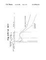
- FIG. 4 is a diagram showing potential changes in the solid state sensor of FIG. 3 in the vertical direction;
- FIG. 5 is a timing chart illustrating a method for driving a solid state image sensor according to the present invention
- FIG. 6 is a diagram showing potential changes when employing the solid state image sensor driving method according to the present invention.
- FIG. 7 is a flowchart illustrating the method for driving the solid state image sensor.
- FIG. 8 schematic block diagram of a timing control circuit according to the present invention.
- the timing controller 30 receives a reference clock signal CK and generates predetermined timing signals (horizontal timing signal HT, vertical timing signal VT and discharge timing signal BT) based on the reference clock signal CK.
- the clock generator 20 generates a vertical transfer clock ⁇ v, a storage transfer clock ⁇ s, and a horizontal transfer clock ⁇ h based on the timing signals HT, VT.
- the clock generator 20 sends the vertical transfer clock ⁇ v and the horizontal transfer clock ⁇ h to the solid state image sensor.
- the clock generator 20 also generates a substrate clock signal ⁇ b in responce to the discharge timing signal BT.
- the timing controller 30 also causes the discharge timing signal BT to rise during the vertical scanning period based on exposure data indicating the exposure level of the solid state image sensor.
- FIGS. 5 to 7 A method for driving a solid state image sensor according to the present invention will now be described with reference to FIGS. 5 to 7 .
- the structure of the solid state image sensor is essentially the same as that of the prior art image sensor shown in FIG. 1 , except that the control signals or clocks generated by the timing controller 3 and the clock generator 2 are activated as described below.
- the frame transfer type solid state image sensor first keeps the transfer electrodes, which form the light-receiving pixels, deactivated and discharges the residing charges.
- the electronic shutter operation then discharges substantially all of the residing information charges.
- the transfer electrodes are then activated to store new information charges.
- a potential well is formed in the channel region below the transfer electrodes so that the functions of the light-receiving pixels become effective.
- the light-receiving pixels function effectively only during the storage period L of the information charges.
- the transfer output of the information charges from the light-receiving section to the storage section, or the frame transfer is set during the blanking period of the vertical sync signal VD.
- the four phase vertical clocks ⁇ v 1 – ⁇ v 4 are fall, which deactivates all of the transfer electrodes.
- the substrate clock ⁇ b is fixed to the low level. This state is maintained until a shutter trigger ST rises.
- the timing of the shutter trigger ST is set based on the exposure level of the image sensor, or the exposure information indicating the average level of the image signal output by the image sensor, in the same manner as the prior art solid state image sensor shown in FIG. 4 .
- the substrate clock ⁇ b rises. This discharges the information charges residing in the channel region below the transfer electrodes toward the substrate.
- the substrate clock ⁇ b remains high over a predetermined period. Unnecessary residual information charges are discharged during this period.
- the first phase and second phase clocks ⁇ v 1 , ⁇ v 2 rise synchronously with the falling of the substrate clock ⁇ b. This forms the potential well below the transfer electrodes to which the vertical transfer clocks ⁇ v 1 , ⁇ v 2 are applied.
- the potential barrier is formed below the transfer electrodes to which the vertical transfer clocks ⁇ v 3 , ⁇ v 4 are applied.
- the rise and fall timing of each vertical transfer clock is set within the horizontal scanning return period to prevent noise from mixing with the image signal.
- the information charges generated by photoelectric conversion in the channel region are stored in the potential well.
- the accumulation of the information charges is maintained during the blanking period of the vertical sync signal VD until the frame transfer is commenced. Accordingly, the information charges generated in the channel regions are stored in the potential well during the period L from when the first and second phase clocks ⁇ v 1 , ⁇ v 2 rise to when the frame transfer is commenced.
- the preferred drive method substantially prevents the formation of the potential well in the channel region during the period from when the frame transfer is completed to when the storage of the information charges is commenced.
- the substrate clock ⁇ b rises to start the shutter operation.
- substantially all of the unnecessary information charges residing in the channel region are discharged even if the shutter operation is fast. This prevents unnecessary information charges from residing in the channel region.
- the amount of charges discharged during the shutter operation is small, the charges are discharged sufficiently even if the potential of the substrate clock ⁇ b is low.
- the discharge of unnecessary charges is completed within a short period of time and unnecessary charges are thus prevented from residing in the channel region when the shutter operation is performed. Furthermore, the small amount of charges that are discharged during the shutter operation allows the voltage required for the shutter operation to be set at a low value. This decreases power consumption.
- all of the transfer electrodes remain deactivated from when the frame transfer is completed to when the storage of the information charges is commenced in order to prevent the formation of the potential well in each channel region.
- the charges generated in the channel regions are discharged toward the substrate regardless of the intensity of the incident light at the channel regions. In other words, all of the charges in the channel regions are easily discharged toward the semiconductor substrate when the potential at the semiconductor substrate increases.
- the preferred embodiment employs four phase vertical transfer clocks. However, three phase or five phase transfer clocks may be employed.
Abstract
An image sensing device includes a solid state image sensor, such as a CCD. An electronic shutter controls the exposure of the sensor to light, and thus the period during which the sensor collects or accumulates an information charge with light receiving pixels. The image sensor includes a semiconductor substrate, a semiconductor layer having parallel channel regions formed on the substrate, and transfer electrodes which intersect the channel regions. The channel regions generate and store the information charges.
Description
The present invention relates to a method and apparatus for driving a solid state image sensor which operates an electronic shutter.
An image sensing apparatus which has a solid state image sensor, like a CCD (Charge Coupled Device), controls the exposure of the solid state image sensor to achieve an optimal exposure state. This exposure control uses an iris mechanism which mechanically controls the amount of incident light to the solid state image sensor in accordance with the luminance of light reflected from a target object. Alternatively, the exposure control can use a so-called electronic shutter which controls the period the solid state image sensor accumlates a charge in accordance with the luminance of light reflected from the target object. The solid state image sensor has light-receiving pixels arranged in a matrix form, which stores (accumlates) information charges that are generated in accordance with the incident light.
A clock generator 2 generates a multi-phase vertical transfer clock φv, a storage transfer clock φs, and a horizontal transfer clock φh in response to horizontal and vertical timing signals HT, VT. The vertical transfer clock φv is sent to the light-receiving section 1 i of the solid state image sensor 1, the storage transfer clock φs is sent to the storage section 1 s, and the horizontal transfer clock φh is sent to the horizontal transfer section 1 h.
When the light-receiving section 1 i receives the vertical transfer clock φv, the stored information charges in each light-receiving pixel of the light-receiving section 1 i are transferred to the storage section is. This is the vertical scanning return period. When the storage section is receives the storage transfer clock φs, the information charges transferred from the light-receiving section 1 i in accordance with the vertical transfer clock φv are acquired by the storage section 1 s. Additionally, the acquired information charges are transferred to the horizontal transfer section 1 h one line at a time. The information charges transferred to the horizontal transfer section 1 h one line at a time in accordance with the storage transfer clock φs are further transferred to the output section 1 d, sequentially. The clock generator 2 also generates a substrate clock φb which rises for a predetermined time period in response to a discharge timing signal BT. The substrate clock φb is applied to the substrate side of the solid state image sensor 1. When the substrate clock φb is active, the information charges stored in the light-receiving pixels of the light-receiving section 1 i are discharged toward the substrate side. Since the vertical transfer clock φv falls synchronously with the rising of the substrate clock φb, the discharge of information charges toward the substrate is smooth.
In this manner, information charges are stored in each light-receiving pixel of the light-receiving section 1 i during a period L, which starts from when the discharge of information charges in accordance with the substrate clock φb is completed to when transmission is commenced by the vertical transfer clock φv. The stored period of the information charges, or the shutter speed, is controlled by adjusting the timing of the substrate clock φb.
A timing controller 3 generates the vertical timing signal VT and the horizontal timing signal HT from a reference clock CK, which has a constant cycle, and sends the signals VT, HT to the clock generator 2. If, for example, the NTSC standard is employed, the timing controller 3 causes the horizontal timing signal HT to rise each time 910 reference clocks CK, which frequency is 14.32 MHz, are counted. The timing controller 3 also causes the vertical timing signal VT to fall each time 525/2 horizontal timing signals HT are counted. The timing controller 3 also causes the discharge timing signal BT to rise during the vertical scanning period based on exposure data indicating the exposure level of the solid state image sensor 1. The timing controller 3, for example, determines whether or not the exposure data, which is obtained by integrating the image signal Y(t) for every single display image unit, is within an optimal range. If the exposure data exceeds the exposure range, the rising timing of the pulse signals is delayed to shorten the storage period L of the information charges. On the other hand, if the exposure data has not yet reached the optimal level, the timing controller 3 advances the rise timing of the pulse signals to prolong the storage period L of the information charges.
The image sensor maintains the image signal Y(t) at an optimal level by changing the length of the period L, during which information charges are stored in the light-receiving section 1 i, in accordance with the level of the image signal Y(t).
In the vertical overflow drain structure, when the light-receiving section 1 i stores information charges, the substrate clock φb is kept low, and one to three of the vertical clocks (φv1–φv4) are kept high. This selectively activates the first and second gate electrodes 15, 16. In the part of the light-receiving section 1 i where the first and second gate electrodes 15, 16 are activated, as shown in FIG. 4 , a potential well (depletion layer) is formed near the buried layer 13. Accordingly, information charges are stored in the region from within the buried layer 13 to the surface of the P-well region 12. In the part of the light-receiving section 1 i where the first and second gate electrodes 15, 16 are deactivated, a potential well is not formed in the buried layer 13 but a potential barrier for defining the light-receiving pixels is formed in the buried layer 13.
During the shutter operation for discharging the information charges stored in each of the light-receiving pixels, all of the vertical clocks φv1–φv4 are kept low and the substrate clock φb rises. Consequently, the potential well in the buried layer 13 becomes shallower while the potential well in the semiconductor substrate 11 becomes deeper. As a result, the potential barrier in the P-well region 12 disappears as indicated by the broken line in FIG. 4 . In this manner, the information charges stored in the potential well in the buried layer 13 are moved to the semiconductor substrate 11 from the buried layer 13 along the potential profile and are discharged therefrom.
In the solid state image sensor 1 having the vertical overflow drain structure, the output section 1 d and the light receiving section 1 i are formed on the same substrate. Thus, the substrate clock φb affects the output portion 1 d during the shutter operation. Accordingly, the rise timing of the substrate clock φb is set within the horizontal scanning return period in order to prevent noise from being mixed with the image signal Y(t) acquired from the output portion 1 d. However, the horizontal scanning return period is very short, lasting only a few microseconds. Hence, if charges are stored in a large number of light-receiving pixels, all of the unnecessary charges in the light-receiving pixels may not be discharged and may thus remain in the light receiving pixels as residual charges. The residual charges may mix with the subsequently stored information charges and decrease the quality of the replayed display image.
Accordingly, it is an objective of the present invention to provide a method and apparatus for driving a solid state image sensor which completely discharges unnecessary charges during the shutter operation.
To achieve the above objective, the present invention provides a method for driving a solid state image sensor that obtains image signals in display image units. The solid state image sensor includes a semiconductor substrate and a semiconductor layer formed on the semiconductor substrate. The semiconductor layer has an opposite conductivity to the semiconductor substrate. The semiconductor layer has a plurality of parallel channel regions arranged therein. A plurality of transfer electrodes are arranged on the semiconductor substrate. Each transfer electrode intersects the plurality of channel regions. Each of the channel regions generates and accumulates information charges. The driving method includes the steps of accumulating information charges in the channel region that correspond to a transfer electrode selected by selectively activating the plurality of transfer electrodes at a predetermined timing during a vertical scanning return period, transferring the accumulated information charges to a transfer register, discharging the information charges in the channel regions toward the semiconductor substrate by keeping the plurality of transfer electrodes deactivated and increasing the potential at the semiconductor substrate, and repetitively executing the accumulating, transferring, and discharging steps to continuously obtain the image signals in display image units.
In a further aspect of the present invention, the present invention provides an apparatus for driving a solid state image sensor that obtains image signals in display image units. The solid state image sensor includes a semiconductor substrate and a semiconductor layer formed on the semiconductor substrate. The semiconductor layer has an opposite conductivity to the semiconductor substrate. The semiconductor layer has a plurality of parallel channel regions arranged therein. A plurality of transfer electrodes are arranged on the semiconductor substrate. Each transfer electrode intersects the plurality of channel regions. Each of the channel regions generates and accumulates information charges. The driving apparatus includes a timing controller for generating a predetermined timing signal based on a reference clock signal, and a clock generator for generating a vertical clock signal and a substrate clock signal based on the timing signal and applying the vertical clock signal and the substrate clock signal to the solid state image sensor. The clock generator activates the vertical clock signal so that the transfer electrodes are selectively activated and the information charges are accumulated in the channel regions corresponding to the activated transfer electrode, and deactivates the vertical clock signal so that the transfer electrodes are maintained in a deactivation state after transfering the stored information charges. The the clock generator further activates the substrate clock signal so that the potential of the semiconductor substrate is increased and the information charges in the channel region are discharged when the transfer electrode is deactivated.
Other aspects and advantages of the present invention will become apparent from the following description, taken in conjunction with the accompanying drawings, illustrating by way of example the principles of the invention.
The features of the present invention that are believed to be novel are set forth with particularity in the appended claims. The invention, together with objects and advantages thereof, may best be understood by reference to the following description of the presently preferred embodiments together with the accompanying drawings in which:
Reffering to FIG. 8 , a clock generator 20 and a timing controller 30 are shown. The timing controller 30 receives a reference clock signal CK and generates predetermined timing signals (horizontal timing signal HT, vertical timing signal VT and discharge timing signal BT) based on the reference clock signal CK. The clock generator 20 generates a vertical transfer clock φv, a storage transfer clock φs, and a horizontal transfer clock φh based on the timing signals HT, VT. The clock generator 20 sends the vertical transfer clock φv and the horizontal transfer clock φh to the solid state image sensor. The clock generator 20 also generates a substrate clock signal φb in responce to the discharge timing signal BT. The timing controller 30 also causes the discharge timing signal BT to rise during the vertical scanning period based on exposure data indicating the exposure level of the solid state image sensor.
A method for driving a solid state image sensor according to the present invention will now be described with reference to FIGS. 5 to 7 . The structure of the solid state image sensor is essentially the same as that of the prior art image sensor shown in FIG. 1 , except that the control signals or clocks generated by the timing controller 3 and the clock generator 2 are activated as described below.
In the driving method according to the present invention, the frame transfer type solid state image sensor first keeps the transfer electrodes, which form the light-receiving pixels, deactivated and discharges the residing charges. The electronic shutter operation then discharges substantially all of the residing information charges. The transfer electrodes are then activated to store new information charges. In other words, when the transfer electrodes are activated in the frame transfer type solid state image sensor, a potential well is formed in the channel region below the transfer electrodes so that the functions of the light-receiving pixels become effective. The light-receiving pixels function effectively only during the storage period L of the information charges.
The transfer output of the information charges from the light-receiving section to the storage section, or the frame transfer is set during the blanking period of the vertical sync signal VD. After the frame transfer is completed, the four phase vertical clocks φv1–φv4 are fall, which deactivates all of the transfer electrodes. In this state, the substrate clock φb is fixed to the low level. This state is maintained until a shutter trigger ST rises. The timing of the shutter trigger ST is set based on the exposure level of the image sensor, or the exposure information indicating the average level of the image signal output by the image sensor, in the same manner as the prior art solid state image sensor shown in FIG. 4 .
As shown in FIG. 5 , when the shutter trigger ST rises during the vertical scanning period, the substrate clock φb rises. This discharges the information charges residing in the channel region below the transfer electrodes toward the substrate. The substrate clock φb remains high over a predetermined period. Unnecessary residual information charges are discharged during this period. Among the four phase vertical transfer clocks φv1–φv4, for example, the first phase and second phase clocks φv1, φv2 rise synchronously with the falling of the substrate clock φb. This forms the potential well below the transfer electrodes to which the vertical transfer clocks φv1, φv2 are applied. The potential barrier is formed below the transfer electrodes to which the vertical transfer clocks φv3, φv4 are applied. The rise and fall timing of each vertical transfer clock is set within the horizontal scanning return period to prevent noise from mixing with the image signal.
The information charges generated by photoelectric conversion in the channel region are stored in the potential well. The accumulation of the information charges is maintained during the blanking period of the vertical sync signal VD until the frame transfer is commenced. Accordingly, the information charges generated in the channel regions are stored in the potential well during the period L from when the first and second phase clocks φv1, φv2 rise to when the frame transfer is commenced.
As shown in FIG. 6A , the preferred drive method substantially prevents the formation of the potential well in the channel region during the period from when the frame transfer is completed to when the storage of the information charges is commenced. Thus, even if incident light in the channel region generates information charges, most of those charges are discharged toward the substrate side. As a result, only the subtle amount of charges residing in the channel region need be discharged toward the substrate side when the substrate clock φb rises to start the shutter operation. Accordingly, substantially all of the unnecessary information charges residing in the channel region are discharged even if the shutter operation is fast. This prevents unnecessary information charges from residing in the channel region. Furthermore, since the amount of charges discharged during the shutter operation is small, the charges are discharged sufficiently even if the potential of the substrate clock φb is low.
In the vertical overflow drain structure solid state image sensor of the preferred embodiment, the discharge of unnecessary charges is completed within a short period of time and unnecessary charges are thus prevented from residing in the channel region when the shutter operation is performed. Furthermore, the small amount of charges that are discharged during the shutter operation allows the voltage required for the shutter operation to be set at a low value. This decreases power consumption.
In the preferred embodiment, all of the transfer electrodes remain deactivated from when the frame transfer is completed to when the storage of the information charges is commenced in order to prevent the formation of the potential well in each channel region. Thus, the charges generated in the channel regions are discharged toward the substrate regardless of the intensity of the incident light at the channel regions. In other words, all of the charges in the channel regions are easily discharged toward the semiconductor substrate when the potential at the semiconductor substrate increases.
The preferred embodiment employs four phase vertical transfer clocks. However, three phase or five phase transfer clocks may be employed.
It should be apparent to those skilled in the art that the present invention may be embodied in many other specific forms without departing from the spirit or scope of the invention. Therefore, the present examples and embodiments are to be considered as illustrative and not restrictive, and the invention is not to be limited to the details given herein, but may be modified within the scope and equivalence of the appended claims.
Claims (7)
1. A method for driving a solid state image sensor that provides image signals in display image units, wherein the solid state image sensor includes a semiconductor substrate, a semiconductor layer formed on the semiconductor substrate and having an opposite conductivity to the semiconductor substrate, the semiconductor layer having a plurality of parallel channel regions arranged therein, and a plurality of transfer electrodes arranged on the semiconductor substrate each intersecting the plurality of channel regions, wherein each of the channel regions generates and accumulates information charges, the driving method comprising the steps of:
storing information charges in the channel region that correspond to a transfer electrode selected by selectively activating the plurality of transfer electrodes at a predetermined timing during a vertical scanning period;
transferring the stored information charges to a transfer register;
deactivating the plurality of transfer electrodes;
discharging, after said deactivating operation, the information charges in the channel regions toward the semiconductor substrate by keeping the plurality of transfer electrodes deactivated and increasing the potential at the semiconductor substrate; and
repetitively executing the storing, transferring, deactivating, and discharging steps to continuously obtain the image signals in display image units.
2. The driving method according to claim 1 , wherein the potential at the semiconductor substrate is raised just before the next storing step.
3. The driving method according to claim 1 , wherein a potential well having a predetermined depth is formed in the selected channel region during the storing step to store the information charges.
4. The driving method according to claim 3 , wherein the potential well is prevented from being formed in the discharging step.
5. An apparatus for driving a solid state image sensor that provides image signals in display image units, wherein the solid state image sensor includes a semiconductor substrate, a semiconductor layer formed on the semiconductor substrate and having an opposite conductivity to the semiconductor substrate, the semiconductor layer having a plurality of parallel channel regions arranged therein, and a plurality of transfer electrodes arranged on the semiconductor substrate each intersecting the plurality of channel regions, wherein each of the channel regions generates and accumulates information charges, the driving apparatus comprising:
a timing controller for generating a predetermined timing signal based on a reference clock signal; and
a clock generator for generating a vertical clock signal and a substrate clock signal based on the timing signal and applying the vertical clock signal and the substrate clock signal to the solid state image sensor, wherein the clock generator activates the vertical clock signal so that the transfer electrodes are selectively activated and the information charges are accumulated in the channel regions corresponding to the activated transfer electrode, deactivates the vertical clock signal so that the transfer electrodes are maintained in a deactivation state after transferring the stored information charges, and then activates the substrate clock signal so that the potential of the semiconductor substrate is increased and the information charges in the channel region are discharged while keeping the plurality of transfer electrodes deactivated.
6. The driving apparatus according to claim 5 , wherein the clock generator activates the substrate clock signal to raise the potential at the semiconductor substrate except when the information charges are stored.
7. The driving apparatus according to claim 5 , wherein the clock generator keeps the substrate clock signal deactivated to keep the plurality of transfer electrodes deactivated except when the information charges are stored.
Applications Claiming Priority (1)
| Application Number | Priority Date | Filing Date | Title |
|---|---|---|---|
| JP10305820A JP2000134546A (en) | 1998-10-27 | 1998-10-27 | Driving method for solid-state image pickup device |
Publications (1)
| Publication Number | Publication Date |
|---|---|
| US6999123B1 true US6999123B1 (en) | 2006-02-14 |
Family
ID=17949773
Family Applications (1)
| Application Number | Title | Priority Date | Filing Date |
|---|---|---|---|
| US09/426,991 Expired - Fee Related US6999123B1 (en) | 1998-10-27 | 1999-10-26 | Method and apparatus for driving solid state image sensor |
Country Status (2)
| Country | Link |
|---|---|
| US (1) | US6999123B1 (en) |
| JP (1) | JP2000134546A (en) |
Cited By (5)
| Publication number | Priority date | Publication date | Assignee | Title |
|---|---|---|---|---|
| US20050206758A1 (en) * | 2004-03-16 | 2005-09-22 | Sanyo Electric Co., Ltd. | Image sensing device employing CCD pixel compression technique and method for driving the same |
| US20050212936A1 (en) * | 2004-03-25 | 2005-09-29 | Eastman Kodak Company | Extended dynamic range image sensor with fixed pattern noise reduction |
| US20070024732A1 (en) * | 2005-07-28 | 2007-02-01 | Akihiro Kuroda | Driving device and driving method for solid state imaging element |
| CN101547319A (en) * | 2008-03-28 | 2009-09-30 | 恩益禧电子股份有限公司 | Solid-state imaging device |
| US20130056618A1 (en) * | 2010-06-14 | 2013-03-07 | Panasonic Corporation | Driving device and spatial information detecting device using the same |
Citations (11)
| Publication number | Priority date | Publication date | Assignee | Title |
|---|---|---|---|---|
| US4281339A (en) * | 1978-06-05 | 1981-07-28 | Nippon Electric Co., Ltd. | Color solid state image pick-up apparatus |
| JPS6350059A (en) | 1986-08-18 | 1988-03-02 | フィリップス エレクトロニクス ネムローゼ フェンノートシャップ | Image pickup device |
| US5144445A (en) * | 1989-12-26 | 1992-09-01 | Sanyo Electric Co., Ltd. | Solid-state image pickup apparatus having a plurality of photoelectric transducers arranged in a matrix |
| US5625414A (en) * | 1995-01-30 | 1997-04-29 | Eastman Kodak Company | Imaging device using asymmetrical timing for pixel summing |
| JPH09168118A (en) * | 1995-12-15 | 1997-06-24 | Nec Corp | Solid state image pickup device |
| US5745808A (en) * | 1995-08-21 | 1998-04-28 | Eastman Kodak Company | Camera exposure control system using variable-length exposure tables |
| JPH10164439A (en) | 1996-11-27 | 1998-06-19 | Sanyo Electric Co Ltd | Image-pickup device |
| US5796432A (en) * | 1993-04-20 | 1998-08-18 | Sony Corporation | Method of and apparatus for solid state imaging device |
| US6229567B1 (en) * | 1996-12-16 | 2001-05-08 | Hyundai Electronics Industries Co., Ltd. | Charge coupled device to enable viewing of a normal or a reverse image |
| US6351284B1 (en) * | 1995-09-29 | 2002-02-26 | Sanyo Electric Co., Ltd. | Method and apparatus for driving solid state image sensor |
| US6545713B1 (en) * | 1997-01-31 | 2003-04-08 | Sanyo Electric Co., Ltd. | Solid-state image pickup apparatus |
-
1998
- 1998-10-27 JP JP10305820A patent/JP2000134546A/en active Pending
-
1999
- 1999-10-26 US US09/426,991 patent/US6999123B1/en not_active Expired - Fee Related
Patent Citations (13)
| Publication number | Priority date | Publication date | Assignee | Title |
|---|---|---|---|---|
| US4281339A (en) * | 1978-06-05 | 1981-07-28 | Nippon Electric Co., Ltd. | Color solid state image pick-up apparatus |
| JPS6350059A (en) | 1986-08-18 | 1988-03-02 | フィリップス エレクトロニクス ネムローゼ フェンノートシャップ | Image pickup device |
| US4769709A (en) | 1986-08-18 | 1988-09-06 | U.S. Philips Corporation | Picture pick-up device including a solid-state image sensor and an electronic shutter |
| US5144445A (en) * | 1989-12-26 | 1992-09-01 | Sanyo Electric Co., Ltd. | Solid-state image pickup apparatus having a plurality of photoelectric transducers arranged in a matrix |
| US5796432A (en) * | 1993-04-20 | 1998-08-18 | Sony Corporation | Method of and apparatus for solid state imaging device |
| US5625414A (en) * | 1995-01-30 | 1997-04-29 | Eastman Kodak Company | Imaging device using asymmetrical timing for pixel summing |
| US5745808A (en) * | 1995-08-21 | 1998-04-28 | Eastman Kodak Company | Camera exposure control system using variable-length exposure tables |
| US6351284B1 (en) * | 1995-09-29 | 2002-02-26 | Sanyo Electric Co., Ltd. | Method and apparatus for driving solid state image sensor |
| JPH09168118A (en) * | 1995-12-15 | 1997-06-24 | Nec Corp | Solid state image pickup device |
| JPH10164439A (en) | 1996-11-27 | 1998-06-19 | Sanyo Electric Co Ltd | Image-pickup device |
| US20030122947A1 (en) | 1996-11-27 | 2003-07-03 | Kazuo Ishimoto | Image pickup apparatus for controlling the discharge of information charges in the image pickup apparatus |
| US6229567B1 (en) * | 1996-12-16 | 2001-05-08 | Hyundai Electronics Industries Co., Ltd. | Charge coupled device to enable viewing of a normal or a reverse image |
| US6545713B1 (en) * | 1997-01-31 | 2003-04-08 | Sanyo Electric Co., Ltd. | Solid-state image pickup apparatus |
Cited By (8)
| Publication number | Priority date | Publication date | Assignee | Title |
|---|---|---|---|---|
| US20050206758A1 (en) * | 2004-03-16 | 2005-09-22 | Sanyo Electric Co., Ltd. | Image sensing device employing CCD pixel compression technique and method for driving the same |
| US20050212936A1 (en) * | 2004-03-25 | 2005-09-29 | Eastman Kodak Company | Extended dynamic range image sensor with fixed pattern noise reduction |
| US20070024732A1 (en) * | 2005-07-28 | 2007-02-01 | Akihiro Kuroda | Driving device and driving method for solid state imaging element |
| CN101547319A (en) * | 2008-03-28 | 2009-09-30 | 恩益禧电子股份有限公司 | Solid-state imaging device |
| US20090242737A1 (en) * | 2008-03-28 | 2009-10-01 | Nec Electronics Corporation | Solid-state imaging device |
| US7964836B2 (en) * | 2008-03-28 | 2011-06-21 | Renesas Electronics Corporation | Solid-state imaging device |
| US20130056618A1 (en) * | 2010-06-14 | 2013-03-07 | Panasonic Corporation | Driving device and spatial information detecting device using the same |
| US9131176B2 (en) * | 2010-06-14 | 2015-09-08 | Panasonic Intellectual Property Management Co., Ltd. | Driving device and spatial information detecting device using the same |
Also Published As
| Publication number | Publication date |
|---|---|
| JP2000134546A (en) | 2000-05-12 |
Similar Documents
| Publication | Publication Date | Title |
|---|---|---|
| US6040859A (en) | Image sensing apparatus and method for discharging dark current charge stored therein | |
| JP3915161B2 (en) | Method for expanding dynamic range of solid-state image sensor with blooming prevention structure and solid-state image sensor | |
| KR100361946B1 (en) | Solid-state imaging device | |
| KR100301886B1 (en) | Solid state imaging device and its driving method | |
| US5463421A (en) | Solid-state image apparatus which sweeps out independently ineffective electric charges so that the exposure period can be varied within a range from one field period to one frame period | |
| US6707499B1 (en) | Technique to increase dynamic range of a CCD image sensor | |
| US6982751B1 (en) | Solid-state imaging apparatus, its driving method, and camera system | |
| US20070146522A1 (en) | Driving method for solid-state image pickup device and image pickup apparatus | |
| EP0403939B1 (en) | Method of driving a solid state imaging device | |
| US4856033A (en) | Solid state imager device with exposure control with noise reduction | |
| US6999123B1 (en) | Method and apparatus for driving solid state image sensor | |
| US7755691B2 (en) | Driving method for solid-state image pickup device and image pickup apparatus | |
| US6351284B1 (en) | Method and apparatus for driving solid state image sensor | |
| KR20050053342A (en) | Solid-state image-taking apparatus, solid-state image-taking system, and apparatus and method for driving the solid-state image-taking apparatus | |
| US4985776A (en) | Method of driving solid-state imaging element | |
| US7379110B2 (en) | Solid-state image pickup device for producing thinned image | |
| US20070131771A1 (en) | Driving method for solid-state image pickup device and image pickup apparatus | |
| US4803555A (en) | Method of driving a solid state image pickup device | |
| US4837629A (en) | Image pickup method using a CCD-type solid state image pickup device with charge dissipation | |
| JP2002290836A (en) | Solid state image sensing device and its driving method | |
| JP3995983B2 (en) | Solid-state imaging device driving method, signal processing method, and substrate voltage adjustment method | |
| JP2771691B2 (en) | Driving method of solid-state imaging device | |
| JPH06178211A (en) | Solid-state image pickup device | |
| JPH07154700A (en) | Solid-state image pickup device | |
| JP2804578B2 (en) | Solid-state imaging device |
Legal Events
| Date | Code | Title | Description |
|---|---|---|---|
| AS | Assignment |
Owner name: SANYO ELECTRIC CO., LTD., JAPAN Free format text: ASSIGNMENT OF ASSIGNORS INTEREST;ASSIGNOR:TAKAHASHI, TATSUYA;REEL/FRAME:010345/0787 Effective date: 19991014 |
|
| REMI | Maintenance fee reminder mailed | ||
| FPAY | Fee payment |
Year of fee payment: 4 |
|
| SULP | Surcharge for late payment | ||
| REMI | Maintenance fee reminder mailed | ||
| LAPS | Lapse for failure to pay maintenance fees | ||
| STCH | Information on status: patent discontinuation |
Free format text: PATENT EXPIRED DUE TO NONPAYMENT OF MAINTENANCE FEES UNDER 37 CFR 1.362 |
|
| FP | Lapsed due to failure to pay maintenance fee |
Effective date: 20140214 |