US7005248B2 - Method of forming cavity between multilayered wirings - Google Patents
Method of forming cavity between multilayered wirings Download PDFInfo
- Publication number
- US7005248B2 US7005248B2 US10/693,972 US69397203A US7005248B2 US 7005248 B2 US7005248 B2 US 7005248B2 US 69397203 A US69397203 A US 69397203A US 7005248 B2 US7005248 B2 US 7005248B2
- Authority
- US
- United States
- Prior art keywords
- alicyclic
- general formula
- bis
- cavity
- polyamic acid
- Prior art date
- Legal status (The legal status is an assumption and is not a legal conclusion. Google has not performed a legal analysis and makes no representation as to the accuracy of the status listed.)
- Expired - Lifetime
Links
- 238000000034 method Methods 0.000 title claims abstract description 79
- 229920000642 polymer Polymers 0.000 claims abstract description 40
- 238000000576 coating method Methods 0.000 claims abstract description 27
- 229920005575 poly(amic acid) Polymers 0.000 claims abstract description 26
- 125000002723 alicyclic group Chemical group 0.000 claims abstract description 25
- 239000011248 coating agent Substances 0.000 claims abstract description 25
- -1 alicyclic diamine Chemical class 0.000 claims abstract description 24
- 239000004642 Polyimide Substances 0.000 claims abstract description 22
- 229920001721 polyimide Polymers 0.000 claims abstract description 22
- 239000004065 semiconductor Substances 0.000 claims abstract description 21
- GTDPSWPPOUPBNX-UHFFFAOYSA-N ac1mqpva Chemical compound CC12C(=O)OC(=O)C1(C)C1(C)C2(C)C(=O)OC1=O GTDPSWPPOUPBNX-UHFFFAOYSA-N 0.000 claims abstract description 19
- 150000000000 tetracarboxylic acids Chemical class 0.000 claims abstract description 19
- 238000010438 heat treatment Methods 0.000 claims abstract description 15
- 239000000758 substrate Substances 0.000 claims abstract description 4
- 238000000059 patterning Methods 0.000 claims abstract description 3
- SECXISVLQFMRJM-UHFFFAOYSA-N N-Methylpyrrolidone Chemical compound CN1CCCC1=O SECXISVLQFMRJM-UHFFFAOYSA-N 0.000 claims description 40
- WFDIJRYMOXRFFG-UHFFFAOYSA-N Acetic anhydride Chemical compound CC(=O)OC(C)=O WFDIJRYMOXRFFG-UHFFFAOYSA-N 0.000 claims description 27
- 239000000203 mixture Substances 0.000 claims description 25
- IMNFDUFMRHMDMM-UHFFFAOYSA-N N-Heptane Chemical compound CCCCCCC IMNFDUFMRHMDMM-UHFFFAOYSA-N 0.000 claims description 20
- JUJWROOIHBZHMG-UHFFFAOYSA-N Pyridine Chemical compound C1=CC=NC=C1 JUJWROOIHBZHMG-UHFFFAOYSA-N 0.000 claims description 18
- 230000004580 weight loss Effects 0.000 claims description 18
- 230000009477 glass transition Effects 0.000 claims description 15
- 239000012298 atmosphere Substances 0.000 claims description 14
- DIOQZVSQGTUSAI-UHFFFAOYSA-N decane Chemical compound CCCCCCCCCC DIOQZVSQGTUSAI-UHFFFAOYSA-N 0.000 claims description 12
- 239000011261 inert gas Substances 0.000 claims description 12
- ISWSIDIOOBJBQZ-UHFFFAOYSA-N Phenol Chemical compound OC1=CC=CC=C1 ISWSIDIOOBJBQZ-UHFFFAOYSA-N 0.000 claims description 11
- 125000004202 aminomethyl group Chemical group [H]N([H])C([H])([H])* 0.000 claims description 11
- QVEIRZNRYOJFCL-UHFFFAOYSA-N 6053-46-9 Chemical compound O=C1OC(=O)C2CC1C1C2CC(=O)OC1=O QVEIRZNRYOJFCL-UHFFFAOYSA-N 0.000 claims description 10
- 239000002184 metal Substances 0.000 claims description 9
- 229910052751 metal Inorganic materials 0.000 claims description 9
- UMJSCPRVCHMLSP-UHFFFAOYSA-N pyridine Natural products COC1=CC=CN=C1 UMJSCPRVCHMLSP-UHFFFAOYSA-N 0.000 claims description 9
- 239000002904 solvent Substances 0.000 claims description 9
- 239000002798 polar solvent Substances 0.000 claims description 8
- FXHOOIRPVKKKFG-UHFFFAOYSA-N N,N-Dimethylacetamide Chemical compound CN(C)C(C)=O FXHOOIRPVKKKFG-UHFFFAOYSA-N 0.000 claims description 7
- 239000003054 catalyst Substances 0.000 claims description 7
- 238000006358 imidation reaction Methods 0.000 claims description 7
- ZMXDDKWLCZADIW-UHFFFAOYSA-N N,N-Dimethylformamide Chemical compound CN(C)C=O ZMXDDKWLCZADIW-UHFFFAOYSA-N 0.000 claims description 6
- ZMANZCXQSJIPKH-UHFFFAOYSA-N Triethylamine Chemical compound CCN(CC)CC ZMANZCXQSJIPKH-UHFFFAOYSA-N 0.000 claims description 6
- 125000001931 aliphatic group Chemical group 0.000 claims description 6
- 125000004432 carbon atom Chemical group C* 0.000 claims description 6
- BSKHPKMHTQYZBB-UHFFFAOYSA-N 2-methylpyridine Chemical compound CC1=CC=CC=N1 BSKHPKMHTQYZBB-UHFFFAOYSA-N 0.000 claims description 4
- YEJRWHAVMIAJKC-UHFFFAOYSA-N 4-Butyrolactone Chemical compound O=C1CCCO1 YEJRWHAVMIAJKC-UHFFFAOYSA-N 0.000 claims description 4
- IAZDPXIOMUYVGZ-UHFFFAOYSA-N Dimethylsulphoxide Chemical compound CS(C)=O IAZDPXIOMUYVGZ-UHFFFAOYSA-N 0.000 claims description 4
- JLTDJTHDQAWBAV-UHFFFAOYSA-N N,N-dimethylaniline Chemical group CN(C)C1=CC=CC=C1 JLTDJTHDQAWBAV-UHFFFAOYSA-N 0.000 claims description 4
- SMWDFEZZVXVKRB-UHFFFAOYSA-N Quinoline Chemical compound N1=CC=CC2=CC=CC=C21 SMWDFEZZVXVKRB-UHFFFAOYSA-N 0.000 claims description 4
- GEQHKFFSPGPGLN-UHFFFAOYSA-N cyclohexane-1,3-diamine Chemical compound NC1CCCC(N)C1 GEQHKFFSPGPGLN-UHFFFAOYSA-N 0.000 claims description 4
- JHIVVAPYMSGYDF-UHFFFAOYSA-N cyclohexanone Chemical compound O=C1CCCCC1 JHIVVAPYMSGYDF-UHFFFAOYSA-N 0.000 claims description 4
- 239000012024 dehydrating agents Substances 0.000 claims description 4
- RLSSMJSEOOYNOY-UHFFFAOYSA-N m-cresol Chemical compound CC1=CC=CC(O)=C1 RLSSMJSEOOYNOY-UHFFFAOYSA-N 0.000 claims description 4
- QAEDZJGFFMLHHQ-UHFFFAOYSA-N trifluoroacetic anhydride Chemical compound FC(F)(F)C(=O)OC(=O)C(F)(F)F QAEDZJGFFMLHHQ-UHFFFAOYSA-N 0.000 claims description 4
- GETQZCLCWQTVFV-UHFFFAOYSA-N trimethylamine Chemical compound CN(C)C GETQZCLCWQTVFV-UHFFFAOYSA-N 0.000 claims description 4
- 239000004793 Polystyrene Substances 0.000 claims description 3
- QLBRROYTTDFLDX-UHFFFAOYSA-N [3-(aminomethyl)cyclohexyl]methanamine Chemical compound NCC1CCCC(CN)C1 QLBRROYTTDFLDX-UHFFFAOYSA-N 0.000 claims description 3
- FOLJMFFBEKONJP-UHFFFAOYSA-N adamantane-1,3-diamine Chemical compound C1C(C2)CC3CC1(N)CC2(N)C3 FOLJMFFBEKONJP-UHFFFAOYSA-N 0.000 claims description 3
- VKIRRGRTJUUZHS-UHFFFAOYSA-N cyclohexane-1,4-diamine Chemical compound NC1CCC(N)CC1 VKIRRGRTJUUZHS-UHFFFAOYSA-N 0.000 claims description 3
- 229920002223 polystyrene Polymers 0.000 claims description 3
- 239000007787 solid Substances 0.000 claims description 3
- AVQQQNCBBIEMEU-UHFFFAOYSA-N 1,1,3,3-tetramethylurea Chemical compound CN(C)C(=O)N(C)C AVQQQNCBBIEMEU-UHFFFAOYSA-N 0.000 claims description 2
- MCTWTZJPVLRJOU-UHFFFAOYSA-N 1-methyl-1H-imidazole Chemical compound CN1C=CN=C1 MCTWTZJPVLRJOU-UHFFFAOYSA-N 0.000 claims description 2
- RNLHGQLZWXBQNY-UHFFFAOYSA-N 3-(aminomethyl)-3,5,5-trimethylcyclohexan-1-amine Chemical compound CC1(C)CC(N)CC(C)(CN)C1 RNLHGQLZWXBQNY-UHFFFAOYSA-N 0.000 claims description 2
- ZZYZUFNSKAIYCJ-UHFFFAOYSA-N 3-[(3-aminocyclohexyl)methyl]cyclohexan-1-amine Chemical compound C1C(N)CCCC1CC1CC(N)CCC1 ZZYZUFNSKAIYCJ-UHFFFAOYSA-N 0.000 claims description 2
- DZIHTWJGPDVSGE-UHFFFAOYSA-N 4-[(4-aminocyclohexyl)methyl]cyclohexan-1-amine Chemical compound C1CC(N)CCC1CC1CCC(N)CC1 DZIHTWJGPDVSGE-UHFFFAOYSA-N 0.000 claims description 2
- BDYVWDMHYNGVGE-UHFFFAOYSA-N [2-(aminomethyl)cyclohexyl]methanamine Chemical compound NCC1CCCCC1CN BDYVWDMHYNGVGE-UHFFFAOYSA-N 0.000 claims description 2
- RXEAFMOPSFWZFL-UHFFFAOYSA-N [3-(aminomethyl)-1-adamantyl]methanamine Chemical compound C1C(C2)CC3CC1(CN)CC2(CN)C3 RXEAFMOPSFWZFL-UHFFFAOYSA-N 0.000 claims description 2
- OXIKYYJDTWKERT-UHFFFAOYSA-N [4-(aminomethyl)cyclohexyl]methanamine Chemical compound NCC1CCC(CN)CC1 OXIKYYJDTWKERT-UHFFFAOYSA-N 0.000 claims description 2
- 125000004018 acid anhydride group Chemical group 0.000 claims description 2
- 125000003277 amino group Chemical group 0.000 claims description 2
- 150000004292 cyclic ethers Chemical group 0.000 claims description 2
- 150000002989 phenols Chemical class 0.000 claims description 2
- WYVAMUWZEOHJOQ-UHFFFAOYSA-N propionic anhydride Chemical compound CCC(=O)OC(=O)CC WYVAMUWZEOHJOQ-UHFFFAOYSA-N 0.000 claims description 2
- 229940124530 sulfonamide Drugs 0.000 claims description 2
- 150000003456 sulfonamides Chemical class 0.000 claims description 2
- 150000003512 tertiary amines Chemical group 0.000 claims description 2
- IMFACGCPASFAPR-UHFFFAOYSA-N tributylamine Chemical compound CCCCN(CCCC)CCCC IMFACGCPASFAPR-UHFFFAOYSA-N 0.000 claims description 2
- YFTHZRPMJXBUME-UHFFFAOYSA-N tripropylamine Chemical compound CCCN(CCC)CCC YFTHZRPMJXBUME-UHFFFAOYSA-N 0.000 claims description 2
- 150000003739 xylenols Chemical class 0.000 claims description 2
- 229920006109 alicyclic polymer Polymers 0.000 description 27
- XUIMIQQOPSSXEZ-UHFFFAOYSA-N Silicon Chemical compound [Si] XUIMIQQOPSSXEZ-UHFFFAOYSA-N 0.000 description 20
- 229910052710 silicon Inorganic materials 0.000 description 20
- 239000010703 silicon Substances 0.000 description 20
- OKKJLVBELUTLKV-UHFFFAOYSA-N Methanol Chemical compound OC OKKJLVBELUTLKV-UHFFFAOYSA-N 0.000 description 18
- 238000005227 gel permeation chromatography Methods 0.000 description 11
- 238000005259 measurement Methods 0.000 description 11
- 239000012299 nitrogen atmosphere Substances 0.000 description 11
- 238000004528 spin coating Methods 0.000 description 11
- 238000003756 stirring Methods 0.000 description 10
- 238000006243 chemical reaction Methods 0.000 description 9
- 238000012545 processing Methods 0.000 description 8
- 230000015572 biosynthetic process Effects 0.000 description 7
- 230000000052 comparative effect Effects 0.000 description 7
- 239000007795 chemical reaction product Substances 0.000 description 6
- 238000000354 decomposition reaction Methods 0.000 description 6
- XKRFYHLGVUSROY-UHFFFAOYSA-N Argon Chemical compound [Ar] XKRFYHLGVUSROY-UHFFFAOYSA-N 0.000 description 4
- IJGRMHOSHXDMSA-UHFFFAOYSA-N Atomic nitrogen Chemical compound N#N IJGRMHOSHXDMSA-UHFFFAOYSA-N 0.000 description 4
- 239000003960 organic solvent Substances 0.000 description 4
- VYPSYNLAJGMNEJ-UHFFFAOYSA-N Silicium dioxide Chemical compound O=[Si]=O VYPSYNLAJGMNEJ-UHFFFAOYSA-N 0.000 description 3
- 238000005530 etching Methods 0.000 description 3
- GEWWCWZGHNIUBW-UHFFFAOYSA-N 1-(4-nitrophenyl)propan-2-one Chemical compound CC(=O)CC1=CC=C([N+]([O-])=O)C=C1 GEWWCWZGHNIUBW-UHFFFAOYSA-N 0.000 description 2
- RDTIGISLOACPEZ-UHFFFAOYSA-N 4,10-dioxatetracyclo[5.5.1.02,6.08,12]tridecane-3,5,9,11-tetrone Chemical compound O=C1OC(=O)C2C1C1C3C(=O)OC(=O)C3C2C1 RDTIGISLOACPEZ-UHFFFAOYSA-N 0.000 description 2
- QGZKDVFQNNGYKY-UHFFFAOYSA-N Ammonia Chemical compound N QGZKDVFQNNGYKY-UHFFFAOYSA-N 0.000 description 2
- 0 O=C1OC(=O)[1*]12C(=O)OC2=O Chemical compound O=C1OC(=O)[1*]12C(=O)OC2=O 0.000 description 2
- 230000003044 adaptive effect Effects 0.000 description 2
- 229910052786 argon Inorganic materials 0.000 description 2
- SWXVUIWOUIDPGS-UHFFFAOYSA-N diacetone alcohol Chemical compound CC(=O)CC(C)(C)O SWXVUIWOUIDPGS-UHFFFAOYSA-N 0.000 description 2
- 238000005516 engineering process Methods 0.000 description 2
- 239000011521 glass Substances 0.000 description 2
- 239000001307 helium Substances 0.000 description 2
- 229910052734 helium Inorganic materials 0.000 description 2
- SWQJXJOGLNCZEY-UHFFFAOYSA-N helium atom Chemical compound [He] SWQJXJOGLNCZEY-UHFFFAOYSA-N 0.000 description 2
- 229910052757 nitrogen Inorganic materials 0.000 description 2
- 230000003071 parasitic effect Effects 0.000 description 2
- 239000000377 silicon dioxide Substances 0.000 description 2
- 230000007704 transition Effects 0.000 description 2
- WZCQRUWWHSTZEM-UHFFFAOYSA-N 1,3-phenylenediamine Chemical compound NC1=CC=CC(N)=C1 WZCQRUWWHSTZEM-UHFFFAOYSA-N 0.000 description 1
- ADLORZDANFZVLO-UHFFFAOYSA-N CC12CC3CC(C1)CC(C)(C3)C2.CC12CC3CC(C1)CC(C14CC5CC(CC(C)(C5)C1)C4)(C3)C2.CC12CC3CC4C1CC1CC2C(C3)C4(C)C1.CCC12CC3CC(C1)CC(CC)(C3)C2.CCC1CC2C3CC(CC)C(C3)C2C1.CCC1CC2CC1C1C(CC)CCC21.CCC1CC2CC1C1CCC(CC)C21 Chemical compound CC12CC3CC(C1)CC(C)(C3)C2.CC12CC3CC(C1)CC(C14CC5CC(CC(C)(C5)C1)C4)(C3)C2.CC12CC3CC4C1CC1CC2C(C3)C4(C)C1.CCC12CC3CC(C1)CC(CC)(C3)C2.CCC1CC2C3CC(CC)C(C3)C2C1.CCC1CC2CC1C1C(CC)CCC21.CCC1CC2CC1C1CCC(CC)C21 ADLORZDANFZVLO-UHFFFAOYSA-N 0.000 description 1
- OBUDJQGMMWEKCD-UHFFFAOYSA-N CC1C(C)C(C)C1C.CC1CC(C)C(C)C1C.CC1CC(C)C(C)CC1C.CC1CC(C)C2C(C)CC(C)C12.CC1CC2C(C)CC(C)C2CC1C.CC1CCC(C)C(C)C1C.CCC1C(C)CC(C)C1C.CCC1CC(C)C(C)CC1C.CCC1CC2C(C)CC(C)C2CC1C Chemical compound CC1C(C)C(C)C1C.CC1CC(C)C(C)C1C.CC1CC(C)C(C)CC1C.CC1CC(C)C2C(C)CC(C)C12.CC1CC2C(C)CC(C)C2CC1C.CC1CCC(C)C(C)C1C.CCC1C(C)CC(C)C1C.CCC1CC(C)C(C)CC1C.CCC1CC2C(C)CC(C)C2CC1C OBUDJQGMMWEKCD-UHFFFAOYSA-N 0.000 description 1
- JDFHVAOHVBMYDK-UHFFFAOYSA-N CC1C(C)C2CC1C(C)C2C.CC1C(C)C2CC1C1C3CC(C(C)C3C)C21.CC1C(C)C2CC1C1CC3C4CC(C(C)C4C)C3C21.CC1CC(C)C2C3CC(C(C)C3C)C12.CC1CC2CC(C)C(C)CC2CC1C.CCC1C(C)C2CC1C(C)C2C.CCC1C(C)C2CC1C1C(C)CC(C)C21.CCC1CC2CC(C)C(C)CC2CC1C.CCC1CCC(C)C(C)C1C Chemical compound CC1C(C)C2CC1C(C)C2C.CC1C(C)C2CC1C1C3CC(C(C)C3C)C21.CC1C(C)C2CC1C1CC3C4CC(C(C)C4C)C3C21.CC1CC(C)C2C3CC(C(C)C3C)C12.CC1CC2CC(C)C(C)CC2CC1C.CCC1C(C)C2CC1C(C)C2C.CCC1C(C)C2CC1C1C(C)CC(C)C21.CCC1CC2CC(C)C(C)CC2CC1C.CCC1CCC(C)C(C)C1C JDFHVAOHVBMYDK-UHFFFAOYSA-N 0.000 description 1
- GYZVNKKRIKDPJN-UHFFFAOYSA-N CC1C(C)C2CC1C1C3CC(C21)C1C2CC(C(C)C2C)C31.CC1C(C)C2CCC1C(C)C2C.CC1C(C)C2OC1C1C(C)C(C)C21.CC1C(C)C2OC1C1C2C2C3OC(C(C)C3C)C12.CCC1(C)CC2CC1C(C)C2C.CCC1C(C)C2CC1C1C3CC(C(C)C3C)C21.CCC1C(C)C2CC1C1C3CC(C4C5CC(C(C)C5C)C34)C21 Chemical compound CC1C(C)C2CC1C1C3CC(C21)C1C2CC(C(C)C2C)C31.CC1C(C)C2CCC1C(C)C2C.CC1C(C)C2OC1C1C(C)C(C)C21.CC1C(C)C2OC1C1C2C2C3OC(C(C)C3C)C12.CCC1(C)CC2CC1C(C)C2C.CCC1C(C)C2CC1C1C3CC(C(C)C3C)C21.CCC1C(C)C2CC1C1C3CC(C4C5CC(C(C)C5C)C34)C21 GYZVNKKRIKDPJN-UHFFFAOYSA-N 0.000 description 1
- VYOBMWHGNWKKLF-UHFFFAOYSA-N CC1C2CCC(C2)C1C.CC1CC2CC(C)C1C2.CC1CC2CC1CC2C.CC1CCCC(CC2CCCC(C)C2)C1.CC1CCCC(CC2CCCCC2C)C1.CC1CCCCC1CC1CCCCC1C.CCC1C2CCC(C2)C1CC.CCC1CC2CC(CC)C1C2.CCC1CC2CC1CC2CC Chemical compound CC1C2CCC(C2)C1C.CC1CC2CC(C)C1C2.CC1CC2CC1CC2C.CC1CCCC(CC2CCCC(C)C2)C1.CC1CCCC(CC2CCCCC2C)C1.CC1CCCCC1CC1CCCCC1C.CCC1C2CCC(C2)C1CC.CCC1CC2CC(CC)C1C2.CCC1CC2CC1CC2CC VYOBMWHGNWKKLF-UHFFFAOYSA-N 0.000 description 1
- PQUBNHHRLGXBID-UHFFFAOYSA-N CC1CC(C)C1.CC1CCC(C)C1.CC1CCC(C)CC1.CC1CCC1C.CC1CCCC(C)C1.CC1CCCC1C.CC1CCCCC1C.CCC1CCC(CC)C1.CCC1CCCC1CC Chemical compound CC1CC(C)C1.CC1CCC(C)C1.CC1CCC(C)CC1.CC1CCC1C.CC1CCCC(C)C1.CC1CCCC1C.CC1CCCCC1C.CCC1CCC(CC)C1.CCC1CCCC1CC PQUBNHHRLGXBID-UHFFFAOYSA-N 0.000 description 1
- LTJDMZJEYRLRKJ-UHFFFAOYSA-N CC1CCC(C2CCC(C)CC2)CC1.CC1CCC(CC2CCC(C)CC2)CC1.CC1CCC(CC2CCCC(C)C2)CC1.CC1CCC(CC2CCCCC2C)CC1.CC1CCCC(C2CCCC(C)C2)C1.CCC1(C)CC(C)CC(C)(C)C1.CCC1CCC(CC)CC1.CCC1CCCC(CC)C1.CCC1CCCCC1CC Chemical compound CC1CCC(C2CCC(C)CC2)CC1.CC1CCC(CC2CCC(C)CC2)CC1.CC1CCC(CC2CCCC(C)C2)CC1.CC1CCC(CC2CCCCC2C)CC1.CC1CCCC(C2CCCC(C)C2)C1.CCC1(C)CC(C)CC(C)(C)C1.CCC1CCC(CC)CC1.CCC1CCCC(CC)C1.CCC1CCCCC1CC LTJDMZJEYRLRKJ-UHFFFAOYSA-N 0.000 description 1
- HZGHFDLUQUQNCC-UHFFFAOYSA-N O=C([N]1(C[IH]C(O2)=O)C2=O)OC1=O Chemical compound O=C([N]1(C[IH]C(O2)=O)C2=O)OC1=O HZGHFDLUQUQNCC-UHFFFAOYSA-N 0.000 description 1
- ATJFFYVFTNAWJD-UHFFFAOYSA-N Tin Chemical compound [Sn] ATJFFYVFTNAWJD-UHFFFAOYSA-N 0.000 description 1
- 239000005456 alcohol based solvent Substances 0.000 description 1
- 229910052782 aluminium Inorganic materials 0.000 description 1
- 229910021529 ammonia Inorganic materials 0.000 description 1
- 239000000010 aprotic solvent Substances 0.000 description 1
- QVGXLLKOCUKJST-UHFFFAOYSA-N atomic oxygen Chemical compound [O] QVGXLLKOCUKJST-UHFFFAOYSA-N 0.000 description 1
- 150000001732 carboxylic acid derivatives Chemical class 0.000 description 1
- 238000007796 conventional method Methods 0.000 description 1
- 229910052802 copper Inorganic materials 0.000 description 1
- 238000000113 differential scanning calorimetry Methods 0.000 description 1
- 238000009792 diffusion process Methods 0.000 description 1
- 238000007865 diluting Methods 0.000 description 1
- 238000003618 dip coating Methods 0.000 description 1
- 230000000694 effects Effects 0.000 description 1
- 238000011156 evaluation Methods 0.000 description 1
- 239000007789 gas Substances 0.000 description 1
- 150000002391 heterocyclic compounds Chemical class 0.000 description 1
- NAQMVNRVTILPCV-UHFFFAOYSA-N hexane-1,6-diamine Chemical compound NCCCCCCN NAQMVNRVTILPCV-UHFFFAOYSA-N 0.000 description 1
- 239000001257 hydrogen Substances 0.000 description 1
- 229910052739 hydrogen Inorganic materials 0.000 description 1
- 125000004435 hydrogen atom Chemical class [H]* 0.000 description 1
- 230000010354 integration Effects 0.000 description 1
- 229910052743 krypton Inorganic materials 0.000 description 1
- DNNSSWSSYDEUBZ-UHFFFAOYSA-N krypton atom Chemical compound [Kr] DNNSSWSSYDEUBZ-UHFFFAOYSA-N 0.000 description 1
- 238000001459 lithography Methods 0.000 description 1
- 239000000463 material Substances 0.000 description 1
- 229910052750 molybdenum Inorganic materials 0.000 description 1
- 229910052754 neon Inorganic materials 0.000 description 1
- GKAOGPIIYCISHV-UHFFFAOYSA-N neon atom Chemical compound [Ne] GKAOGPIIYCISHV-UHFFFAOYSA-N 0.000 description 1
- 239000001301 oxygen Substances 0.000 description 1
- 229910052760 oxygen Inorganic materials 0.000 description 1
- 238000007747 plating Methods 0.000 description 1
- 230000001737 promoting effect Effects 0.000 description 1
- 229910052704 radon Inorganic materials 0.000 description 1
- SYUHGPGVQRZVTB-UHFFFAOYSA-N radon atom Chemical compound [Rn] SYUHGPGVQRZVTB-UHFFFAOYSA-N 0.000 description 1
- 238000005507 spraying Methods 0.000 description 1
- 238000006467 substitution reaction Methods 0.000 description 1
- 229910052721 tungsten Inorganic materials 0.000 description 1
- XLYOFNOQVPJJNP-UHFFFAOYSA-N water Substances O XLYOFNOQVPJJNP-UHFFFAOYSA-N 0.000 description 1
- 229910001868 water Inorganic materials 0.000 description 1
- 229910052724 xenon Inorganic materials 0.000 description 1
- FHNFHKCVQCLJFQ-UHFFFAOYSA-N xenon atom Chemical compound [Xe] FHNFHKCVQCLJFQ-UHFFFAOYSA-N 0.000 description 1
Images

Classifications
-
- H—ELECTRICITY
- H01—ELECTRIC ELEMENTS
- H01L—SEMICONDUCTOR DEVICES NOT COVERED BY CLASS H10
- H01L21/00—Processes or apparatus adapted for the manufacture or treatment of semiconductor or solid state devices or of parts thereof
- H01L21/70—Manufacture or treatment of devices consisting of a plurality of solid state components formed in or on a common substrate or of parts thereof; Manufacture of integrated circuit devices or of parts thereof
- H01L21/71—Manufacture of specific parts of devices defined in group H01L21/70
- H01L21/768—Applying interconnections to be used for carrying current between separate components within a device comprising conductors and dielectrics
- H01L21/76801—Applying interconnections to be used for carrying current between separate components within a device comprising conductors and dielectrics characterised by the formation and the after-treatment of the dielectrics, e.g. smoothing
- H01L21/7682—Applying interconnections to be used for carrying current between separate components within a device comprising conductors and dielectrics characterised by the formation and the after-treatment of the dielectrics, e.g. smoothing the dielectric comprising air gaps
-
- H—ELECTRICITY
- H01—ELECTRIC ELEMENTS
- H01L—SEMICONDUCTOR DEVICES NOT COVERED BY CLASS H10
- H01L21/00—Processes or apparatus adapted for the manufacture or treatment of semiconductor or solid state devices or of parts thereof
- H01L21/70—Manufacture or treatment of devices consisting of a plurality of solid state components formed in or on a common substrate or of parts thereof; Manufacture of integrated circuit devices or of parts thereof
- H01L21/71—Manufacture of specific parts of devices defined in group H01L21/70
- H01L21/768—Applying interconnections to be used for carrying current between separate components within a device comprising conductors and dielectrics
-
- H—ELECTRICITY
- H01—ELECTRIC ELEMENTS
- H01L—SEMICONDUCTOR DEVICES NOT COVERED BY CLASS H10
- H01L21/00—Processes or apparatus adapted for the manufacture or treatment of semiconductor or solid state devices or of parts thereof
- H01L21/70—Manufacture or treatment of devices consisting of a plurality of solid state components formed in or on a common substrate or of parts thereof; Manufacture of integrated circuit devices or of parts thereof
- H01L21/71—Manufacture of specific parts of devices defined in group H01L21/70
- H01L21/76—Making of isolation regions between components
- H01L21/764—Air gaps
-
- H—ELECTRICITY
- H01—ELECTRIC ELEMENTS
- H01L—SEMICONDUCTOR DEVICES NOT COVERED BY CLASS H10
- H01L23/00—Details of semiconductor or other solid state devices
- H01L23/52—Arrangements for conducting electric current within the device in operation from one component to another, i.e. interconnections, e.g. wires, lead frames
- H01L23/522—Arrangements for conducting electric current within the device in operation from one component to another, i.e. interconnections, e.g. wires, lead frames including external interconnections consisting of a multilayer structure of conductive and insulating layers inseparably formed on the semiconductor body
- H01L23/5222—Capacitive arrangements or effects of, or between wiring layers
-
- H—ELECTRICITY
- H01—ELECTRIC ELEMENTS
- H01L—SEMICONDUCTOR DEVICES NOT COVERED BY CLASS H10
- H01L23/00—Details of semiconductor or other solid state devices
- H01L23/52—Arrangements for conducting electric current within the device in operation from one component to another, i.e. interconnections, e.g. wires, lead frames
- H01L23/522—Arrangements for conducting electric current within the device in operation from one component to another, i.e. interconnections, e.g. wires, lead frames including external interconnections consisting of a multilayer structure of conductive and insulating layers inseparably formed on the semiconductor body
- H01L23/532—Arrangements for conducting electric current within the device in operation from one component to another, i.e. interconnections, e.g. wires, lead frames including external interconnections consisting of a multilayer structure of conductive and insulating layers inseparably formed on the semiconductor body characterised by the materials
- H01L23/5329—Insulating materials
-
- H—ELECTRICITY
- H01—ELECTRIC ELEMENTS
- H01L—SEMICONDUCTOR DEVICES NOT COVERED BY CLASS H10
- H01L23/00—Details of semiconductor or other solid state devices
- H01L23/48—Arrangements for conducting electric current to or from the solid state body in operation, e.g. leads, terminal arrangements ; Selection of materials therefor
- H01L23/482—Arrangements for conducting electric current to or from the solid state body in operation, e.g. leads, terminal arrangements ; Selection of materials therefor consisting of lead-in layers inseparably applied to the semiconductor body
- H01L23/4821—Bridge structure with air gap
-
- H—ELECTRICITY
- H01—ELECTRIC ELEMENTS
- H01L—SEMICONDUCTOR DEVICES NOT COVERED BY CLASS H10
- H01L2924/00—Indexing scheme for arrangements or methods for connecting or disconnecting semiconductor or solid-state bodies as covered by H01L24/00
- H01L2924/0001—Technical content checked by a classifier
- H01L2924/0002—Not covered by any one of groups H01L24/00, H01L24/00 and H01L2224/00
-
- H—ELECTRICITY
- H01—ELECTRIC ELEMENTS
- H01L—SEMICONDUCTOR DEVICES NOT COVERED BY CLASS H10
- H01L2924/00—Indexing scheme for arrangements or methods for connecting or disconnecting semiconductor or solid-state bodies as covered by H01L24/00
- H01L2924/10—Details of semiconductor or other solid state devices to be connected
- H01L2924/11—Device type
- H01L2924/12—Passive devices, e.g. 2 terminal devices
- H01L2924/1204—Optical Diode
- H01L2924/12044—OLED
Definitions
- the present invention relates to a method of forming a cavity between wirings using a heat decomposable alicyclic polymer that is a polyamic acid and/or a polyimide obtained by reacting a specific alicyclic tetracarboxylic acid dianhydride and a specific alicyclic diamine, reveals a specific heat resistant temperature and a specific heat decomposition temperature, and can readily form a cavity structure between metallic wirings in, for example, semiconductors.
- a heat decomposable alicyclic polymer that is a polyamic acid and/or a polyimide obtained by reacting a specific alicyclic tetracarboxylic acid dianhydride and a specific alicyclic diamine, reveals a specific heat resistant temperature and a specific heat decomposition temperature, and can readily form a cavity structure between metallic wirings in, for example, semiconductors.
- silica (SiO 2 ) films formed by the vacuum process such as the CVD process have widely been employed as a dielectric film in semiconductors, etc.
- coating type dielectric films containing a tetraalkoxysilane hydrolyzate as the major component and called an SOG (Spin on Glass) film are employed mainly for the purpose of flattening.
- SOG Spin on Glass
- an object of the present invention is to provide a method that can readily form a cavity structure between metallic wirings in, for example, semiconductors using a polyamic acid and/or a polyimide obtained by reacting a specific alicyclic tetracarboxylic acid dianhydride and a specific alicyclic diamine.
- the method comprises:
- the FIGURE is a view showing a process of the formation method of a cavity between metallic wirings according to the present invention.
- a cavity-forming polymer between multilayered wirings used the present invention is a polyamic acid and/or a polyimide obtained from at least one alicyclic tetracarboxylic acid dianhydride represented by the following general formula (1) and at least one alicyclic diamine represented by the following general formula (2).
- General Formula (2) is a polyamic acid and/or a polyimide obtained from at least one alicyclic tetracarboxylic acid dianhydride represented by the following general formula (1) and at least one alicyclic diamine represented by the following general formula (2).
- R 1 represents a tetravalent alicyclic hydrocarbon group having 4–20 carbon atoms.
- the tetravalent alicyclic hydrocarbon group can contain a cyclic ether structure in the molecule.
- R 2 represents a divalent alicyclic hydrocarbon group having 4–20 carbon atoms.
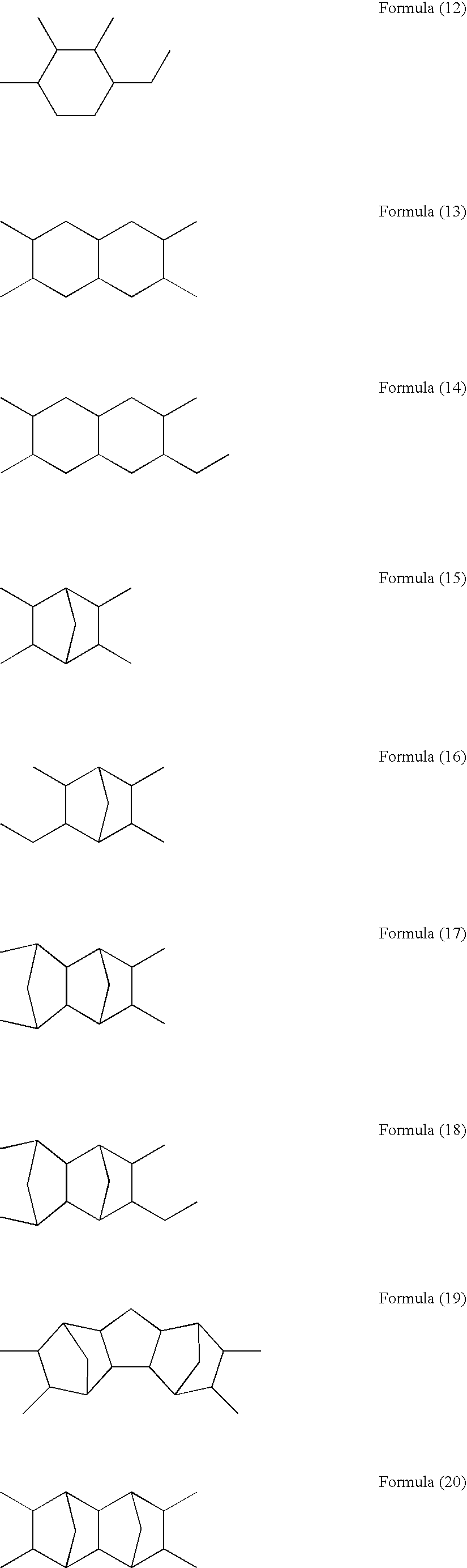
- Examples of the tetravalent alicyclic hydrocarbon group having 4–20 carbon atoms represented by R 1 in the general formula (1) include tetravalent alicyclic hydrocarbon groups represented by the following formulae (3) to (27).
- alicyclic tetracarboxylic acid dianhydride represented by the general formula (1) and containing one of the tetravalent alicyclic hydrocarbon groups represented by the formulae (3) to (27).
- the alicyclic tetracarboxylic acid dianhydride can be used alone or as mixtures of two or more thereof.
- Examples of the divalent alicyclic hydrocarbon group having 4–20 carbon atoms represented by R 2 in the general formula (2) include divalent alicyclic hydrocarbon groups represented by the following formulae (28) to (61).
- the polyamic acid and/or the polyimide that is the cavity-forming polymer between metallic wirings is prepared by the following method.
- At least one aliphatic tetracarboxylic acid dianhydride represented by the general formula (1) and at least one alicyclic diamine represented by the general formula (2) are reacted in an aprotic polar solvent and/or a phenol based solvent in a solids concentration of 1–30% by weight at a temperature in the range of 0–150° C. for 1–24 hours, to obtain a polyamic acid solution.
- a dehydrating agent in an amount of 1–20 moles per mole of the aliphatic tetracarboxylic acid dianhydride represented by the general formula (1) and an imidation catalyst in an amount of 0.5–30 moles per mole of the aliphatic tetracarboxylic acid dianhydride represented by the general formula (1) are added to react the resulting polyamic acid solution at a temperature in the range of 0–180° C. for 1–24 hours.
- a polyimide solution is obtained.
- the polyimide that can be used includes polyimides in which the polyamic acid is partially imidated.
- the polyamic acid solution and/or the polyimide solution used in the present invention can be substituted with other organic solvent by the conventional procedure, if desired.
- the aprotic polar solvent used in the present invention is not particularly limited so far as it can dissolve the polyamic acid formed by the reaction therein.
- Preferred examples of the aprotic polar solvent include ⁇ -butyrolactone, cyclohexanone, N-methyl-2- pyrrolidone, N,N-dimethylacetamide, N,N-dimethylformamide, dimethyl sulfoxide, tetramethylurea, and hexamethyl sulfonamide.
- the phenol based solvent used in the present invention is not particularly limited so far as it can dissolve the polyamic acid formed by the reaction therein.
- Preferred examples phenol based include m-cresol, xylenol, phenol, and halogenated phenols.
- the alicyclic tetracarboxylic acid dianhydride represented by the general formula (1) and the alicyclic diamine represented by the general formula (2) while adjusting the use proportion such that the amount of the acid anhydride group in the alicyclic tetracarboxylic acid anhydride is 0.2–2 equivalents, and preferably 0.7–1.3 equivalents, to one equivalent of the amino group in the alicyclic diamine compound.
- the dehydrating agent used in the present invention is not particularly limited so far as it can be dissolved or dispersed in the aprotic polar solvent and/or phenol based solvent.
- Preferred examples include acetic anhydride, propionic anhydride, and trifluoroacetic anhydride.
- the imidation catalyst used in the invention is not particularly limited so far as it is a tertiary amine that can be dissolved or dispersed in the aprotic polar solvent and/or phenol based solvent.
- Preferred examples include aliphatic tertiary amines such as trimethylamine, triethylamine, tripropylamine or tributylamine; aromatic tertiary amines such as N,N-dimethylaniline; and heterocyclic compounds such as pyridine, 2-methylpyridine, N-methylimidazole or quinoline.
- substitution solvent used in the present invention is not particularly limited so far as it is an organic solvent that can dissolve the polyamic acid and/or polyimide therein.
- Preferred examples include the above-described aprotic solvents, the above-described phenol based solvents, and alcohol based solvents such as diacetone alcohol.
- the polyamic acid and/or polyimide synthesized according to the above method preferably has a weight average molecular weight, as reduced into polystyrene measured by gel permeation chromatography, in the range of 1,000–500,000.
- a weight average molecular weight as reduced into polystyrene measured by gel permeation chromatography
- heat resistance of the resulting polymer may be insufficient, or the solution viscosity increases so that handling properties such as coating properties may be lowered, and hence, such is not preferable.
- the alicyclic polymer used in the present invention has a weight loss on heating at 350° C. for one hour in an inert gas atmosphere and/or a vacuum atmosphere of 5% by weight or less and a weight loss on heating at 500° C. for one hour in an inert gas atmosphere and/or a vacuum atmosphere of 80% by weight or more.
- the heat decomposable alicyclic polymer having a specific heat resistant temperature and a specific heat decomposition temperature can be removed only by simple heat treatment and has a mechanical strength that is sufficiently adaptive to the wiring processing process at temperatures of the heat resistant temperature or lower. Accordingly, it is possible to readily form a cavity structure between metallic wirings in semiconductors, etc., by using the alicyclic polymer of the present invention.
- the inert gas examples include rare gases such as helium, neon, argon, krypton, xenon or radon, and nitrogen.
- the inert gas generally used has a purity of 99.9% or more.
- the inert gas having a purity of 99.99% or more is preferably used, and the inert gas having a purity of 99.999% or more is particularly preferably used.
- Preferable examples of the inert gas used are nitrogen, argon, and helium.
- the vacuum atmosphere is usually 100 Torr or less, preferably 10 Torr or less, and more preferably 1 Torr or less.
- the alicyclic polymer used in the present invention usually has a weight loss on heating at 350° C. for one hour in an inert gas atmosphere and/or a vacuum atmosphere of 5% by weight or less, preferably 3% by weight or less, and more preferably 1% by weight or less.
- the alicyclic polymer is thermally stable at a temperature of 350° C. or lower at which processing of metallic wirings, etc., of semiconductor devices is usually carried out and therefore, is preferable as a material for formation processing of semiconductor devices.
- the alicyclic polymer usually has a weight loss on heating at 500° C. for one hour in an inert gas atmosphere and/or a vacuum atmosphere of 80% by weight or more, preferably 90% by weight or more, and more preferably 95% by weight or more.
- an inert gas atmosphere 80% by weight or more, preferably 90% by weight or more, and more preferably 95% by weight or more.
- the amount of the component incorporated is not particularly limited but is usually 50% by volume or less, and preferably 25% by volume or less.
- the alicyclic polymer has good heat decomposition properties at 500° C. or lower and can be removed only by a simple heat treatment without necessity of an operation, such as etching or icing, that is usually employed during the formation processing of semiconductor devices. This makes it possible to easily form a cavity structure between metallic wirings in semiconductor devices, etc.
- the alicyclic polymer usually has a glass transition temperature of 200° C. or higher, preferably 220° C. or higher, and more preferably 240° C. or higher. As described above, the alicyclic polymer has a high glass transition temperature, and hence, is preferable from the standpoints that even when exposed to high temperatures during the formation of metallic wirings in the semiconductor device, it does not exhibit a large change in volume following phase transition and keeps stability of the wiring shape.
- the alicyclic polymer has a mechanical strength sufficiently endurable to the formation processing of semiconductors. Specifically, since the alicyclic polymer usually has a hardness of 0.2 GPa or more, preferably 0.3 GPa or more, and more preferably 0.4 GPa or more, and usually has an elastic modulus of 5.0 GPa or more, preferably 6.0 GPa or more, and more preferably 7.0 GPa or more, it can be adapted to the formation processing of semiconductor devices such CMP.
- the alicyclic polymer can be processed into a film shape and provided for the use.
- the film of the alicyclic polymer can be obtained by diluting the polyamic acid and/or polyimide with an organic solvent, etc., forming the solution into a film shape by various processes such as a spin coating process, a dip coating process, a roll coating process, a flow coating process, a spray coating process or a hot press process, and optionally heating at a temperature of the heat decomposition temperature or lower of the alicyclic polymer to remove the unnecessary organic solvent.
- the alicyclic polymer makes it possible to easily form a cavity structure between metallic wirings in semiconductor devices, etc.
- the alicyclic polymer is applied to the surface of a prescribed first dielectric film of a semiconductor substrate (see FIG. 1A ).
- the alicyclic polymer is patterned in a space for forming a metallic wiring using the conventional lithography technology and etching technology (see FIG. 1B ).
- a metal such as Cu, Al, W or Mo is embedded in the pattern formed on the alicyclic polymer by the conventional method such as plating or CVD (see FIG. 1C ).
- a layer of TaN, TiN, etc. may be formed between the alicyclic polymer and the metal.
- the surface can be flattened by CMP.
- a second dielectric film is formed on the alicyclic polymer having the metal embedded therein by the conventional spin process, CVD process or the like (see FIG. 1D ).
- the alicyclic polymer is removed upon heating, whereby a cavity can be formed between the metallic wirings (see FIG. 1E ).
- the removal of the alicyclic polymer can be carried out every layer of the multilayered metallic wirings or by repeating the steps of FIG. 1A to FIG. 1D and then getting together some layers.
- a weight average molecular weight as reduced into polystyrene was measured by the GPC process.
- thermogravity (TG) process Upon heating in a nitrogen atmosphere at an arbitrary temperature for one hour, a change in weight was measured by the thermogravity (TG) process.
- a glass transition temperature was measured by the differential scanning calorimetry (DSC) process.
- the measurement was carried out by the nonaindentation process.
- Tthe reaction product was poured into a large amount of methanol to solidify a polymer, which was then recovered and dried at 80° C. overnight.
- the resulting polymer was found to have a weight average molecular weight of 23,000.
- the resulting polymer was dissolved in N,N-dimethylacetamide (DMAc), and the solution was applied to a silicon wafer by the spin coating process.
- the silicon wafer was heat treated at 350° C. for 30 minutes to obtain a transparent coating film having a film thickness of about 1 ⁇ m. This coating film was measured with respect to weight loss, glass transition temperature, elastic modulus and hardness according to the above-described methods. The results obtained are shown in the Table below.
- the reaction product was poured into a large amount of methanol to solidify a polymer, which was then recovered and dried at 80° C. overnight.
- the resulting polymer was found to have a weight average molecular weight of 21,000.
- the resulting polymer was dissolved in ⁇ -butyrolactone (GBL), and the solution was applied to a silicon wafer by the spin coating process.
- the silicon wafer was heat treated at 350° C. for 30 minutes to obtain a transparent coating film having a film thickness of about 1 ⁇ m. This coating film was measured with respect to weight loss, glass transition temperature, elastic modulus and hardness according to the above methods. The results obtained are shown in the Table below.
- the reaction product was poured into a large amount of methanol to solidify a polymer, which was then recovered and dried at 80° C. overnight.
- the resulting polymer was found to have a weight average molecular weight of 19,000.
- the resulting polymer was dissolved in DMAc, and the solution was applied to a silicon wafer by the spin coating process.
- the silicon wafer was heat treated at 350° C. for 30 minutes to obtain a transparent coating film having a film thickness of 1 ⁇ m. This coating film was measured with respect to weight loss, glass transition temperature, elastic modulus and hardness according to the above methods. The results obtained are shown in the Table below.
- the reaction product was poured into a large amount of methanol to solidify a polymer, which was then recovered and dried at 80° C. overnight.
- the resulting polymer was found to have a weight average molecular weight of 25,000.
- the resulting polymer was dissolved in DMAc, and the solution was applied to a silicon wafer by the spin coating process.
- the silicon wafer was heat treated at 350° C. for 30 minutes to obtain a transparent coating film having a film thickness of about 1 ⁇ m. This coating film was measured with respect to weight loss, glass transition temperature, elastic modulus and hardness according to the above methods. The results obtained are shown in the Table below.
- the resulting polymer was found to have a weight average molecular weight of 900.
- the resulting polymer solution was concentrated in vacuo so as to have a solids concentration of about 20% by weight and applied to a silicon wafer by the spin coating process.
- the silicon wafer was heat treated at 350° C. for 30 minutes to obtain a transparent coating film having a film thickness of about 1 ⁇ m.
- This coating film was measured with respect to weight loss, glass transition temperature, elastic modulus and hardness according to the above methods. The results obtained are shown in the Table below.
- the reaction product was poured into a large amount of methanol to solidify a polymer, which was then recovered and dried at 80° C. overnight.
- the resulting polymer was found to have a weight average molecular weight of 23,000.
- the resulting polymer was dissolved in ⁇ -butyrolactone (GBL), and the solution was applied to a silicon wafer by the spin coating process.
- the silicon wafer was heat treated at 350° C. for 30 minutes to obtain a transparent coating film having a film thickness of about 1 ⁇ m. This coating film was measured with respect to weight loss, glass transition temperature, elastic modulus and hardness according to the above methods. The results obtained are shown in the Table below.
- the reaction product was poured into a large amount of methanol to solidify a polymer, which was then recovered and dried at 80° C. overnight.
- the resulting polymer was found to have a weight average molecular weight of 18,000.
- the resulting polymer was dissolved in DMAc, and the solution was applied to a silicon wafer by the spin coating process.
- the silicon wafer was heat treated at 350° C. for 30 minutes to obtain a transparent coating film having a film thickness of 1 ⁇ m. This coating film was measured with respect to weight loss, glass transition temperature, elastic modulus and hardness according to the above methods. The results obtained are shown in the Table below.
- the present invention relates to an alicyclic polymer obtained by reacting a specific alicyclic tetracarboxylic acid dianhydride and a specific alicyclic diamine and to a process of producing the same. Since the alicyclic polymer has a specific heat resistant temperature and a specific heat decomposition temperature, it can be removed only by simple heat treatment and has a mechanical strength that is sufficiently adaptive to the wiring processing process at temperatures of the heat resistant temperature or lower. Accordingly, it is possible to readily form a cavity structure between metallic wirings in semiconductors, etc., by using the alicyclic polymer.
Abstract
A method that can readily form a cavity structure between metallic wirings in, for example, semiconductors using a polyamic acid and/or a polyimide obtained by reacting a specific alicyclic tetracarboxylic acid dianhydride and a specific alicyclic diamine. The method includes a step of coating the surface of a first dielectric film formed on a semiconductor substrate with a polyamic acid and/or a polyimide, a step of patterning a cavity-forming polymer between the multilayered wirings, a step of forming a second dielectric film on the cavity-forming polymer between the multilayered wirings containing a metallic wiring, and a step of removing the cavity-forming polymer between the multilayered wirings by heating to form a cavity between the metallic wirings.
Description
The present invention relates to a method of forming a cavity between wirings using a heat decomposable alicyclic polymer that is a polyamic acid and/or a polyimide obtained by reacting a specific alicyclic tetracarboxylic acid dianhydride and a specific alicyclic diamine, reveals a specific heat resistant temperature and a specific heat decomposition temperature, and can readily form a cavity structure between metallic wirings in, for example, semiconductors.
Hitherto, silica (SiO2) films formed by the vacuum process such as the CVD process have widely been employed as a dielectric film in semiconductors, etc. Further, coating type dielectric films containing a tetraalkoxysilane hydrolyzate as the major component and called an SOG (Spin on Glass) film are employed mainly for the purpose of flattening. In recent years, following large scale integration of semiconductor devices and the like, a demand for low dielectric constant dielectric films is increasing for the purpose of reducing a wiring parasitic capacitance to improve the wiring delay. However, since relatively minute films are obtained by the CVD process, it is difficult to obtain a low dielectric constant of 2.5 or less. According to realization of a high porosity of SOG, since the dielectric constant increases with an increase in hygroscopicity following the realization of a high porosity, the effect of realizing a low dielectric constant by a reduction of film density is cancelled so that it is difficult to obtain low-dielectric constant films. While dielectric films with a low dielectric constant containing a polyorganosiloxane as the major component and called organic SOG are developed, in the case where it is intended to obtain a low dielectric constant of 2.3 or less, there is a problem such that a film strength necessary for formation processing of semiconductor devices is not obtained.
As the method of reducing a wiring parasitic capacitance, there are proposed semiconductor devices having a cavity between wirings as described in, for example, JP-A-9-172068, JP-A-8-83839, and JP-A-2001-85519.
However, according to these prior art methods, after preparing a structure in which a space between metallic wirings is filled with an organic resist or a silica compound, the organic resist or the silica compound is removed by etching or icing to form a cavity between the metallic wirings, and hence, a problem involved that the operation is complicated.
Accordingly, an object of the present invention is to provide a method that can readily form a cavity structure between metallic wirings in, for example, semiconductors using a polyamic acid and/or a polyimide obtained by reacting a specific alicyclic tetracarboxylic acid dianhydride and a specific alicyclic diamine.
The method comprises:
a step of coating the surface of a first dielectric film formed on a semiconductor substrate with a polyamic acid and/or a polyimide obtained from at least one alicyclic tetracarboxylic acid dianhydride represented by the general formula (1) shown hereinafter and at least one alicyclic diamine represented by the general formula (2) shown hereinafter,
a step of patterning the polyamic acid and/or the polyimide as a cavity-forming polymer,
a step of forming a second dielectric film on the cavity-forming polymer containing a metallic wiring, and
a step of removing the cavity-forming polymer between the multilayered wirings by heating to form a cavity between the metallic wirings.
The FIGURE is a view showing a process of the formation method of a cavity between metallic wirings according to the present invention.
In the drawing:
1: Dielectric film 1
2: Polymer
3: Metal
4: Dielectric film 2
5: Cavity
The present invention will be described in detail below.
A cavity-forming polymer between multilayered wirings used the present invention is a polyamic acid and/or a polyimide obtained from at least one alicyclic tetracarboxylic acid dianhydride represented by the following general formula (1) and at least one alicyclic diamine represented by the following general formula (2). 
General Formula (2)
General Formula (2)
H2N—R2—NH2
In the formula (1), R1 represents a tetravalent alicyclic hydrocarbon group having 4–20 carbon atoms. The tetravalent alicyclic hydrocarbon group can contain a cyclic ether structure in the molecule. In the formula (2), R2 represents a divalent alicyclic hydrocarbon group having 4–20 carbon atoms.
Examples of the tetravalent alicyclic hydrocarbon group having 4–20 carbon atoms represented by R1 in the general formula (1) include tetravalent alicyclic hydrocarbon groups represented by the following formulae (3) to (27). 

It is particularly preferable to use 4,10-dioxatricyclo[6.3.1.02,7]-dodecane-3,5,9,11-tetraone as the alicyclic tetracarboxylic acid dianhydride represented by the general formula (1) and containing one of the tetravalent alicyclic hydrocarbon groups represented by the formulae (3) to (27). The alicyclic tetracarboxylic acid dianhydride can be used alone or as mixtures of two or more thereof.
Examples of the divalent alicyclic hydrocarbon group having 4–20 carbon atoms represented by R2 in the general formula (2) include divalent alicyclic hydrocarbon groups represented by the following formulae (28) to (61). 


It is preferable to use 1,3-diaminocyclohexane, 1,4-diaminocyclohexane, 1,2-bisaminomethylcyclohexane, 1,3-bisaminomethylcyclohexane, 1,4-bisaminomethylcyclohexane, isophoronediamine, 4,4′-diaminobiscyclohexyl, 3,3′-diaminobiscyclohexyl, bis(4-aminocyclohexyl)methane, bis(3-aminocyclohexyl)methane, 2,6-diamino-dicyclo[2.2.1]heptane, 2,5-diamino-dicyclo[2.2.1 ]heptane, 2,3-bis(aminomethyl)-dicyclo[2.2.1]heptane, 2,5-bis(aminomethyl)-dicyclo[2.2.1]heptane, 2,6-bis(aminomethyl)-dicyclo[2.2.1]-heptane, 3,9-bis(aminomethyl)-tricyclo[6.2.1.02,6]decane, 4,9-bis(aminomethyl)-tricyclo[6.2.1.02,6]decane, 5,9-bis(aminomethyl)-tricyclo [6.2.1.02,6]decane, 1,3-diaminoadamantane, or 1,3-bis(aminomethyl)adamantane as the alicyclic diamine represented by the general formula (2) and containing one of the divalent alicyclic hydrocarbon groups represented by the formulae (28) to (61). The alicyclic diamine can be used alone or as mixtures of two or more thereof.
The polyamic acid and/or the polyimide that is the cavity-forming polymer between metallic wirings is prepared by the following method.
First of all, at least one aliphatic tetracarboxylic acid dianhydride represented by the general formula (1) and at least one alicyclic diamine represented by the general formula (2) are reacted in an aprotic polar solvent and/or a phenol based solvent in a solids concentration of 1–30% by weight at a temperature in the range of 0–150° C. for 1–24 hours, to obtain a polyamic acid solution. If required and necessary, a dehydrating agent in an amount of 1–20 moles per mole of the aliphatic tetracarboxylic acid dianhydride represented by the general formula (1) and an imidation catalyst in an amount of 0.5–30 moles per mole of the aliphatic tetracarboxylic acid dianhydride represented by the general formula (1) are added to react the resulting polyamic acid solution at a temperature in the range of 0–180° C. for 1–24 hours. Thus, a polyimide solution is obtained. In the present invention, it is not always required for the polyamic acid used to be entirely imidated, but the polyimide that can be used includes polyimides in which the polyamic acid is partially imidated. The polyamic acid solution and/or the polyimide solution used in the present invention can be substituted with other organic solvent by the conventional procedure, if desired.
The aprotic polar solvent used in the present invention is not particularly limited so far as it can dissolve the polyamic acid formed by the reaction therein. Preferred examples of the aprotic polar solvent include γ-butyrolactone, cyclohexanone, N-methyl-2- pyrrolidone, N,N-dimethylacetamide, N,N-dimethylformamide, dimethyl sulfoxide, tetramethylurea, and hexamethyl sulfonamide.
The phenol based solvent used in the present invention is not particularly limited so far as it can dissolve the polyamic acid formed by the reaction therein. Preferred examples phenol based include m-cresol, xylenol, phenol, and halogenated phenols.
In the invention, it is preferable to use the alicyclic tetracarboxylic acid dianhydride represented by the general formula (1) and the alicyclic diamine represented by the general formula (2) while adjusting the use proportion such that the amount of the acid anhydride group in the alicyclic tetracarboxylic acid anhydride is 0.2–2 equivalents, and preferably 0.7–1.3 equivalents, to one equivalent of the amino group in the alicyclic diamine compound.
The dehydrating agent used in the present invention is not particularly limited so far as it can be dissolved or dispersed in the aprotic polar solvent and/or phenol based solvent. Preferred examples include acetic anhydride, propionic anhydride, and trifluoroacetic anhydride.
The imidation catalyst used in the invention is not particularly limited so far as it is a tertiary amine that can be dissolved or dispersed in the aprotic polar solvent and/or phenol based solvent. Preferred examples include aliphatic tertiary amines such as trimethylamine, triethylamine, tripropylamine or tributylamine; aromatic tertiary amines such as N,N-dimethylaniline; and heterocyclic compounds such as pyridine, 2-methylpyridine, N-methylimidazole or quinoline.
The substitution solvent used in the present invention is not particularly limited so far as it is an organic solvent that can dissolve the polyamic acid and/or polyimide therein. Preferred examples include the above-described aprotic solvents, the above-described phenol based solvents, and alcohol based solvents such as diacetone alcohol.
The polyamic acid and/or polyimide synthesized according to the above method preferably has a weight average molecular weight, as reduced into polystyrene measured by gel permeation chromatography, in the range of 1,000–500,000. When the molecular weight range falls outside the range, heat resistance of the resulting polymer may be insufficient, or the solution viscosity increases so that handling properties such as coating properties may be lowered, and hence, such is not preferable.
It is possible to adjust the molecular weight of the polyamic acid and/or polyimide by adjusting the amounts of the alicyclic tetracarboxylic acid dianhydride and the alicyclic diamine used and further by properly adding a carboxylic acid monoanhydride or a monoamine, if required and necessary.
The alicyclic polymer used in the present invention has a weight loss on heating at 350° C. for one hour in an inert gas atmosphere and/or a vacuum atmosphere of 5% by weight or less and a weight loss on heating at 500° C. for one hour in an inert gas atmosphere and/or a vacuum atmosphere of 80% by weight or more. The heat decomposable alicyclic polymer having a specific heat resistant temperature and a specific heat decomposition temperature can be removed only by simple heat treatment and has a mechanical strength that is sufficiently adaptive to the wiring processing process at temperatures of the heat resistant temperature or lower. Accordingly, it is possible to readily form a cavity structure between metallic wirings in semiconductors, etc., by using the alicyclic polymer of the present invention.
Examples of the inert gas include rare gases such as helium, neon, argon, krypton, xenon or radon, and nitrogen. The inert gas generally used has a purity of 99.9% or more. The inert gas having a purity of 99.99% or more is preferably used, and the inert gas having a purity of 99.999% or more is particularly preferably used. Preferable examples of the inert gas used are nitrogen, argon, and helium. The vacuum atmosphere is usually 100 Torr or less, preferably 10 Torr or less, and more preferably 1 Torr or less.
The alicyclic polymer used in the present invention usually has a weight loss on heating at 350° C. for one hour in an inert gas atmosphere and/or a vacuum atmosphere of 5% by weight or less, preferably 3% by weight or less, and more preferably 1% by weight or less. The alicyclic polymer is thermally stable at a temperature of 350° C. or lower at which processing of metallic wirings, etc., of semiconductor devices is usually carried out and therefore, is preferable as a material for formation processing of semiconductor devices.
The alicyclic polymer usually has a weight loss on heating at 500° C. for one hour in an inert gas atmosphere and/or a vacuum atmosphere of 80% by weight or more, preferably 90% by weight or more, and more preferably 95% by weight or more. For the sake of promoting the decomposition of the alicyclic polymer, it is possible to incorporate hydrogen, oxygen, ammonia, water, etc., in the inert gas atmosphere. The amount of the component incorporated is not particularly limited but is usually 50% by volume or less, and preferably 25% by volume or less. The alicyclic polymer has good heat decomposition properties at 500° C. or lower and can be removed only by a simple heat treatment without necessity of an operation, such as etching or icing, that is usually employed during the formation processing of semiconductor devices. This makes it possible to easily form a cavity structure between metallic wirings in semiconductor devices, etc.
The alicyclic polymer usually has a glass transition temperature of 200° C. or higher, preferably 220° C. or higher, and more preferably 240° C. or higher. As described above, the alicyclic polymer has a high glass transition temperature, and hence, is preferable from the standpoints that even when exposed to high temperatures during the formation of metallic wirings in the semiconductor device, it does not exhibit a large change in volume following phase transition and keeps stability of the wiring shape.
The alicyclic polymer has a mechanical strength sufficiently endurable to the formation processing of semiconductors. Specifically, since the alicyclic polymer usually has a hardness of 0.2 GPa or more, preferably 0.3 GPa or more, and more preferably 0.4 GPa or more, and usually has an elastic modulus of 5.0 GPa or more, preferably 6.0 GPa or more, and more preferably 7.0 GPa or more, it can be adapted to the formation processing of semiconductor devices such CMP.
If desired, the alicyclic polymer can be processed into a film shape and provided for the use. The film of the alicyclic polymer can be obtained by diluting the polyamic acid and/or polyimide with an organic solvent, etc., forming the solution into a film shape by various processes such as a spin coating process, a dip coating process, a roll coating process, a flow coating process, a spray coating process or a hot press process, and optionally heating at a temperature of the heat decomposition temperature or lower of the alicyclic polymer to remove the unnecessary organic solvent.
Using the alicyclic polymer makes it possible to easily form a cavity structure between metallic wirings in semiconductor devices, etc. Specifically, for example, the alicyclic polymer is applied to the surface of a prescribed first dielectric film of a semiconductor substrate (see FIG. 1A ). The alicyclic polymer is patterned in a space for forming a metallic wiring using the conventional lithography technology and etching technology (see FIG. 1B ). A metal such as Cu, Al, W or Mo is embedded in the pattern formed on the alicyclic polymer by the conventional method such as plating or CVD (see FIG. 1C ). For the purpose of preventing diffusion of the metal during embedding the metal, a layer of TaN, TiN, etc., may be formed between the alicyclic polymer and the metal. After embedding the metal, the surface can be flattened by CMP. A second dielectric film is formed on the alicyclic polymer having the metal embedded therein by the conventional spin process, CVD process or the like (see FIG. 1D ). Finally, the alicyclic polymer is removed upon heating, whereby a cavity can be formed between the metallic wirings (see FIG. 1E ). The removal of the alicyclic polymer can be carried out every layer of the multilayered metallic wirings or by repeating the steps of FIG. 1A to FIG. 1D and then getting together some layers.
The present invention is described in more detail by reference to the following Examples. However, the Examples merely describe a summary of the embodiments of the present invention, and it should not be construed that the invention is limited thereto without particular reasons.
All parts and percentages in the Examples and Comparative Example are parts by weight and % by weight, respectively, unless otherwise indicated.
Various evaluations were carried out in the following methods.
Weight Average Molecular Weight:
A weight average molecular weight as reduced into polystyrene was measured by the GPC process.
Weight Loss:
Upon heating in a nitrogen atmosphere at an arbitrary temperature for one hour, a change in weight was measured by the thermogravity (TG) process.
Glass Transition Temperature:
A glass transition temperature was measured by the differential scanning calorimetry (DSC) process.
Elastic Modulus and Hardness:
The measurement was carried out by the nonaindentation process.
In an N2 atmosphere, 13.47 g of 1,3-diaminocyclohexane was dissolved in 400 ml of N-methyl-2-pyrrolidone (NMP), and 26.90 g of 4,10-dioxatricyclo[6.3.1.02,7]-dodecane-3,5,9, 11-tetraone was added to and suspended in the solution at 25° C. with stirring. The temperature was raised to 50° C., and the mixture was reacted for 6 hours. 400 ml of NMP was added to the reaction solution, and 48.17 g of acetic anhydride and 37.97 g of pyridine were then added thereto. The resulting mixture was reacted at 135° C. for 2 hours. Tthe reaction product was poured into a large amount of methanol to solidify a polymer, which was then recovered and dried at 80° C. overnight. As a result of the measurement by the GPC process, the resulting polymer was found to have a weight average molecular weight of 23,000. The resulting polymer was dissolved in N,N-dimethylacetamide (DMAc), and the solution was applied to a silicon wafer by the spin coating process. The silicon wafer was heat treated at 350° C. for 30 minutes to obtain a transparent coating film having a film thickness of about 1 μm. This coating film was measured with respect to weight loss, glass transition temperature, elastic modulus and hardness according to the above-described methods. The results obtained are shown in the Table below.
In an N2 atmosphere, 13.47 g of 1,4-diaminocyclohexane was dissolved in 400 ml of NMP, and 26.90 g of 4,10-dioxatricyclo [6.3.1.02,7]dodecane-3,5,9,11-tetraone was added to and suspended in the solution at 25° C. with stirring. The temperature was raised to 50° C., and the mixture was reacted for 6 hours. As a result of the measurement by the GPC process, the resulting polymer was found to have a weight average molecular weight of 26,000. The resulting polymer solution was applied to a silicon wafer by the spin coating process. The silicon wafer was heat treated at 350° C. for 30 minutes to obtain a transparent coating film having a film thickness of about 1 μm. This coating film was measured with respect to weight loss, glass transition temperature, elastic modulus and hardness according to the above methods. The results obtained are shown in the Table below.
In an N2 atmosphere, 16.78 g of 1,3-bis(aminomethyl)cyclohexane was dissolved in 400 ml of NMP, and 26.90 g of 4,10-dioxatricyclo[6.3.1.02,7]dodecane-3,5,9,11-tetraone was a added to and suspended in the solution at 25° C. with stirring. The temperature was raised to 50° C., and the mixture was reacted for 6 hours. 400 ml of NMP was added to the reaction solution, and 48.17 g of acetic anhydride and 37.97 g of pyridine were then added thereto. The mixture was reacted at 135° C. for 4 hours. The reaction product was poured into a large amount of methanol to solidify a polymer, which was then recovered and dried at 80° C. overnight. As a result of the measurement by the GPC process, the resulting polymer was found to have a weight average molecular weight of 21,000. The resulting polymer was dissolved in γ-butyrolactone (GBL), and the solution was applied to a silicon wafer by the spin coating process. The silicon wafer was heat treated at 350° C. for 30 minutes to obtain a transparent coating film having a film thickness of about 1 μm. This coating film was measured with respect to weight loss, glass transition temperature, elastic modulus and hardness according to the above methods. The results obtained are shown in the Table below.
In an N2 atmosphere, 18.20 g of 2,6-bis(aminomethyl)dicyclo[2.2.1]heptane was dissolved in 400 ml of NMP, and 26.90 g of 4,10-dioxatricyclo[6.3.1.02,7]dodecane-3,5,9,11-tetraone was added to and suspended in the solution at 25° C. with stirring. The temperature was raised to 50° C., and the mixture was reacted for 6 hours. 400 ml of NMP was added to the reaction solution, and 48.17 g of acetic anhydride and 37.97 g of pyridine were then added thereto. The mixture was reacted at 135° C. for 4 hours. The reaction product was poured into a large amount of methanol to solidify a polymer, which was then recovered and dried at 80° C. overnight. As a result of the measurement by the GPC process, the resulting polymer was found to have a weight average molecular weight of 19,000. The resulting polymer was dissolved in DMAc, and the solution was applied to a silicon wafer by the spin coating process. The silicon wafer was heat treated at 350° C. for 30 minutes to obtain a transparent coating film having a film thickness of 1 μm. This coating film was measured with respect to weight loss, glass transition temperature, elastic modulus and hardness according to the above methods. The results obtained are shown in the Table below.
In an N2 atmosphere, 19.62 g of 1,3-diaminoadamantane was dissolved in 400 ml of NMP, and 26.90 g of 4,10-dioxatricyclo[6.3.1.02,7]dodecane-3,5,9,11-tetraone was added to and suspended in the solution at 25° C. with stirring. The temperature was raised to 50° C., and the mixture was reacted for 6 hours. 400 ml of NMP was added to the reaction solution, and 48.17 g of acetic anhydride and 37.97 g of pyridine were then added thereto. The mixture was reacted at 135° C. for 2 hours. The reaction product was poured into a large amount of methanol to solidify a polymer, which was then recovered and dried at 80° C. overnight. As a result of the measurement by the GPC process, the resulting polymer was found to have a weight average molecular weight of 25,000. The resulting polymer was dissolved in DMAc, and the solution was applied to a silicon wafer by the spin coating process. The silicon wafer was heat treated at 350° C. for 30 minutes to obtain a transparent coating film having a film thickness of about 1 μm. This coating film was measured with respect to weight loss, glass transition temperature, elastic modulus and hardness according to the above methods. The results obtained are shown in the Table below.
In an N2 atmosphere, 13.47 g of 1,3-diaminocyclohexane was dissolved in 200 ml of NMP, and 28.34 g of 4,10-dioxatetracyclo[5.5.1 .02,6.08,12]tridecane-3,5,9,11-tetraone was added to and suspended in the solution at 25° C. with stirring. The temperature was raised to 50° C., and the mixture was reacted for 6 hours. As a result of the measurement by the GPC process, the resulting polymer was found to have a weight average molecular weight of 28,000. The resulting polymer solution was applied to a silicon wafer by the spin coating process. The silicon wafer was heat treated at 350° C. for 30 minutes to obtain a transparent coating film having a film thickness of about 1 μm. This coating film was measured with respect to weight loss, glass transition temperature, elastic modulus and hardness according to the above methods. The results obtained are shown in the Table below.
In an N2 atmosphere, 18.20 g of 2,6-bis(aminomethyl)dicyclo[2.2.1]heptane was dissolved in 200 ml of NMP, and 28.34 g of 4,10-dioxatetracyclo[5.5.1.02,6.08,12]-tridecane-3,5,9, 11tetraone was added to and suspended in the solution at 25° C. with stirring. The temperature was raised to 50° C., and the mixture was reacted for 6 hours. As a result of the measurement by the GPC process, the resulting polymer was found to have a weight average molecular weight of 26,000. The resulting polymer solution was applied to a silicon wafer by the spin coating process. The silicon wafer was heat treated at 350° C. for 30 minutes to obtain a transparent coating film having a film thickness of about 1 μm. This coating film was measured with respect to weight loss, glass transition temperature, elastic modulus and hardness according to the above methods. The results obtained are shown in the Table below.
In an N2 atmosphere, 11.42 g of 1,3-diaminocycloxeane was dissolved in 400 ml of NMP, and 33.63 g of 4,10-dioxatricyclo[6.3.1.02,7]dodecane-3,5,9,11-tetraone was added to and suspended in the solution at 25° C. with stirring. The temperature was raised to 50° C., and the mixture was reacted for 6 hours. 400 ml of NMP was added to the reaction solution, and 61.26 g of acetic anhydride and 47.47 g of pyridine were then added thereto. The mixture was reacted at 135° C. for 2 hours. As a result of the measurement by the GPC process, the resulting polymer was found to have a weight average molecular weight of 900. The resulting polymer solution was concentrated in vacuo so as to have a solids concentration of about 20% by weight and applied to a silicon wafer by the spin coating process. The silicon wafer was heat treated at 350° C. for 30 minutes to obtain a transparent coating film having a film thickness of about 1 μm. This coating film was measured with respect to weight loss, glass transition temperature, elastic modulus and hardness according to the above methods. The results obtained are shown in the Table below.
In an N2 atmosphere, 13.71 g of 1,6-diaminohexane was dissolved in 400 ml of NMP, and 26.90 g of 4,10-dioxatricyclo[6.3.1.02,7]dodecane-3,5,9,11-tetraone was added to and suspended in the solution at 25° C. with stirring. The temperature was raised to 50° C., and the mixture was reacted for 6 hours. 400 ml of NMP was added to the reaction solution, and 48.17 g of acetic anhydride and 37.97 g of pyridine were then added thereto. The mixture was reacted at 135° C. for 4 hours. The reaction product was poured into a large amount of methanol to solidify a polymer, which was then recovered and dried at 80° C. overnight. As a result of the measurement by the GPC process, the resulting polymer was found to have a weight average molecular weight of 23,000. The resulting polymer was dissolved in γ-butyrolactone (GBL), and the solution was applied to a silicon wafer by the spin coating process. The silicon wafer was heat treated at 350° C. for 30 minutes to obtain a transparent coating film having a film thickness of about 1 μm. This coating film was measured with respect to weight loss, glass transition temperature, elastic modulus and hardness according to the above methods. The results obtained are shown in the Table below.
In an N2 atmosphere, 12.76 g of 1,3-diaminobenzene was dissolved in 400 ml of NMP, and 26.90 g of 4,10-dioxatricyclo[6.3.1.02,7]dodecane-3,5,9,11-tetraone was added to and suspended in the solution at 25° C. with stirring. The temperature was raised to 50° C., and the mixture was reacted for 6 hours. 400 ml of NMP was added to the reaction solution, and 48.17 g of acetic anhydride and 37.97 g of pyridine were then added thereto. The mixture was reacted at 135° C. for 4 hours. The reaction product was poured into a large amount of methanol to solidify a polymer, which was then recovered and dried at 80° C. overnight. As a result of the measurement by the C process, the resulting polymer was found to have a weight average molecular weight of 18,000. The resulting polymer was dissolved in DMAc, and the solution was applied to a silicon wafer by the spin coating process. The silicon wafer was heat treated at 350° C. for 30 minutes to obtain a transparent coating film having a film thickness of 1 μm. This coating film was measured with respect to weight loss, glass transition temperature, elastic modulus and hardness according to the above methods. The results obtained are shown in the Table below.
| TABLE | ||||||
| Weight average | Weight loss (%) | Glass | Elastic | |||
| molecular | At | At | transition | modulus | Hardness | ||
| weight | 350° C. | 500° C. | temperature (° C.) | (GPa) | (GPa) | ||
| Example 1 | 23000 | 0.5 | 95 | >250 | 8.0 | 0.4 |
| Example 2 | 26000 | 0.6 | 95 | >250 | 7.8 | 0.4 |
| Example 3 | 21000 | 0.9 | 97 | >250 | 7.6 | 0.4 |
| Example 4 | 19000 | 0.7 | 96 | >250 | 8.5 | 0.5 |
| Example 5 | 25000 | 0.9 | 96 | >250 | 8.1 | 0.4 |
| Example 6 | 28000 | 0.8 | 97 | >250 | 7.7 | 0.4 |
| Example 7 | 26000 | 0.6 | 96 | >250 | 7.5 | 0.4 |
| Comparative | 900 | 5.5 | 97 | >250 | 7.1 | 0.3 |
| Example 1 | ||||||
| Comparative | 23000 | 6.3 | 97 | 230 | 5.0 | 0.2 |
| Example 2 | ||||||
| Comparative | 18000 | 0.7 | 72 | >250 | 7.9 | 0.4 |
| Example 3 | ||||||
The present invention relates to an alicyclic polymer obtained by reacting a specific alicyclic tetracarboxylic acid dianhydride and a specific alicyclic diamine and to a process of producing the same. Since the alicyclic polymer has a specific heat resistant temperature and a specific heat decomposition temperature, it can be removed only by simple heat treatment and has a mechanical strength that is sufficiently adaptive to the wiring processing process at temperatures of the heat resistant temperature or lower. Accordingly, it is possible to readily form a cavity structure between metallic wirings in semiconductors, etc., by using the alicyclic polymer.
Claims (18)
1. A method of forming a cavity between multilayered wirings, comprising:
coating the surface of a first dielectric film formed on a semiconductor substrate with a polyamic acid and/or a polyimide obtained from at least one alicyclic tetracarboxylic acid dianhydride represented by the following general formula (1) and at least one alicyclic diamine represented by the following general formula (2): 
wherein R1 represents a tetravalent alicyclic hydrocarbon group having 4–20 carbon atoms, the tetravalent alicyclic hydrocarbon group being able to contain a cyclic ether structure in the molecule, and
H2N—R2—NH2 (2)
H2N—R2—NH2 (2)
wherein R2 represents a divalent alicyclic hydrocarbon group having 4–20 carbon atoms,
patterning the polyamic acid and/or the polyimide as a cavity-forming polymer,
embedding a metal in a pattern in the cavity-forming polymer to form a metallic wiring layer,
forming a second dielectric film on the cavity-forming polymer containing the embedded metal, and
removing the cavity-forming polymer present in the wiring layer by heating to form a cavity.
2. The method as claimed in claim 1 , wherein the polyamic acid and/or the polyimide has a weight average molecular weight, as reduced into polystyrene, in the range of 1,000–500,000.
3. The method as claimed in claim 1 , wherein the polyamic acid and/or the polyimide has a weight loss on heating at 350° C. for one hour in an inert gas atmosphere and/or a vacuum atmosphere of 5% by weight or less and a weight loss on heating at 500° C. for one hour in an inert gas atmosphere and/or a vacuum atmosphere of 80% by weight or more.
4. The method as claimed in claim 1 , wherein the polyamic acid and/or the polyimide has a glass transition temperature of 200° C. or higher.
5. The method as claimed in claim 1 , wherein the polyamic acid and/or the polyimide has an elastic modulus at 25° C. of 5 GPa or more.
6. The method as claimed in claim 1 , wherein said alicyclic tetracarboxylic acid dianhydride represented by the general formula (1) is 4,10-dioxatricyclo [6.3.1.02,7]-dodecane- 3,5,9,11 -tetraone.
7. The method as claimed in claim 1 , wherein said alicyclic diamine represented by the general formula (2) is a member selected from the group consisting of 1,3-diaminocyclohexane, 1,4-diaminocyclohexane, 1,2-bisaminomethylcyclohexane, 1,3-bisaminomethylcyclohexane, 1,4-bisaminomethylcyclo-hexane, isophoronediamine, 4,4′-diaminobiscyclohexyl, 3,3′-diaminobiscyclohexyl, bis(4-aminocyclohexyl) methane, bis(3-aminocyclohexyl)methane, 2,6-diamino-dicyclo[2.2.1]-heptane, 2,5-diamino-dicyclo[2.2.1]heptane, 2,3-bis(aminomethyl)-dicyclo[2.2.1]heptane, 2,5-bis(aminomethyl)-dicyclo[2.2.1]heptane, 2,6-bis(aminomethyl)-dicyclo[2.2.1]heptane, 3,9-bis(aminomethyl)-tricyclo[6.2.1.02,6]decane, 4,9-bis(aminomethyl)-tricyclo [6.2.1.02,6]decane, 5,9-bis(aminomethyl)- tricyclo[6.2.1.02,6]decane, 1,3-diamino-adamantane, or 1,3-bis(aminomethyl)adamantane and mixtures thereof.
8. The method as claimed in claim 1 , wherein said aliphatic tetracarboxylic acid dianhydride represented by the general formula (1) and said alicyclic diamine represented by the general formula (2) are reacted in an aprotic polar solvent and/or a phenol based solvent in a solids concentration of 1–30 % by weight at a temperature in the range of 0–150° C. for 1–24 hours, to obtain a polyamic acid solution.
9. The method as claimed in claim 8 , further comprising:
adding a dehydrating agent in an amount of 1–20 moles per mole of the aliphatic tetracarboxylic acid dianhydride represented by the general formula (1).
10. The method as claimed in claim 9 , wherein said dehydrating agent is selected from the group consisting of acetic anhydride, propionic anhydride, trifluoroacetic anhydride and mixtures thereof.
11. The method as claimed in claim 9 , wherein said imidation catalyst is a tertiary amine that can be dissolved or dispersed in the aprotic polar solvent and/or phenol based solvent.
12. The method as claimed in claim 9 , wherein said imidation catalyst is an aliphatic tertiary amine selected from the group consisting of trimethylamine, triethylamine, tripropylamine, tributylamine and mixtures thereof.
13. The method as claimed in claim 9 , wherein said imidation catalyst is N,N-dimethylaniline.
14. The method as claimed in claim 9 , wherein said imidation catalyst is selected from the group consisting of pyridine, 2-methylpyridine, N- methylimidazole, quinoline and mixtures thereof.
15. The method as claimed in claim 8 , further comprising:
adding an imidation catalyst in an amount of 0.5–30 moles per mole of the aliphatic tetracarboxylic acid dianhydride represented by the general formula (1).
16. The method as claimed in claim 8 , wherein said aprotic polar solvent is selected from the group consisting of γ-butyrolactone, cyclohexanone, N-methyl-2- pyrrolidone, N,N-dimethylacetamide, N,N-dimethylformamide, dimethyl sulfoxide, tetramethylurea, hexamethyl sulfonamide and mixtures thereof.
17. The method as claimed in claim 8 , wherein said phenol based solvent is selected from the group consisting of m-cresol, xylenol, phenol, halogenated phenols and mixtures thereof.
18. The method as claimed in claim 1 , wherein said alicyclic tetracarboxylic acid dianhydride represented by the general formula (1) and said alicyclic diamine represented by the general formula (2) are used in a proportion so that an amount of the acid anhydride group in the alicyclic tetracarboxylic acid anhydride is 0.2–2 equivalents to one equivalent of the amino group in the alicyclic diamine compound.
Applications Claiming Priority (2)
| Application Number | Priority Date | Filing Date | Title |
|---|---|---|---|
| JP2002-314248 | 2002-10-29 | ||
| JP2002314248A JP3775375B2 (en) | 2002-10-29 | 2002-10-29 | Cavity formation method between multilayer wiring |
Publications (2)
| Publication Number | Publication Date |
|---|---|
| US20040092127A1 US20040092127A1 (en) | 2004-05-13 |
| US7005248B2 true US7005248B2 (en) | 2006-02-28 |
Family
ID=32105369
Family Applications (1)
| Application Number | Title | Priority Date | Filing Date |
|---|---|---|---|
| US10/693,972 Expired - Lifetime US7005248B2 (en) | 2002-10-29 | 2003-10-28 | Method of forming cavity between multilayered wirings |
Country Status (6)
| Country | Link |
|---|---|
| US (1) | US7005248B2 (en) |
| EP (1) | EP1418618B1 (en) |
| JP (1) | JP3775375B2 (en) |
| KR (1) | KR101062556B1 (en) |
| DE (1) | DE60329741D1 (en) |
| TW (1) | TWI248450B (en) |
Cited By (1)
| Publication number | Priority date | Publication date | Assignee | Title |
|---|---|---|---|---|
| US20090272295A1 (en) * | 2005-09-28 | 2009-11-05 | Central Glass Company, Limited | Coating Materials Consisting of Low- or Medium-Molecular Organic Compounds |
Families Citing this family (12)
| Publication number | Priority date | Publication date | Assignee | Title |
|---|---|---|---|---|
| WO2008007629A1 (en) * | 2006-07-10 | 2008-01-17 | Nissan Chemical Industries, Ltd. | Polyamic acid and polyimide |
| JP5040254B2 (en) * | 2006-10-18 | 2012-10-03 | 東洋紡績株式会社 | Polyimide resin and flexible wiring board using the same |
| JP2008243907A (en) * | 2007-03-26 | 2008-10-09 | Jsr Corp | Composition for forming cavity between conductive layers, sacrifice film for forming cavity between conductive layers, and method of forming cavity between conductive layers |
| US8946048B2 (en) | 2010-06-19 | 2015-02-03 | Sandisk Technologies Inc. | Method of fabricating non-volatile memory with flat cell structures and air gap isolation |
| US8492224B2 (en) | 2010-06-20 | 2013-07-23 | Sandisk Technologies Inc. | Metal control gate structures and air gap isolation in non-volatile memory |
| US8778749B2 (en) * | 2011-01-12 | 2014-07-15 | Sandisk Technologies Inc. | Air isolation in high density non-volatile memory |
| US9123714B2 (en) | 2012-02-16 | 2015-09-01 | Sandisk Technologies Inc. | Metal layer air gap formation |
| KR20130111154A (en) * | 2012-03-30 | 2013-10-10 | 주식회사 엘지화학 | Substrate for organic electronic device |
| US9123577B2 (en) | 2012-12-12 | 2015-09-01 | Sandisk Technologies Inc. | Air gap isolation in non-volatile memory using sacrificial films |
| US9349740B2 (en) | 2014-01-24 | 2016-05-24 | Sandisk Technologies Inc. | Non-volatile storage element with suspended charge storage region |
| JP7390194B2 (en) | 2020-01-17 | 2023-12-01 | 東京エレクトロン株式会社 | Air gap formation method |
| CN112501593B (en) * | 2020-10-29 | 2022-09-30 | 长芯科技(上海)有限公司 | Manufacturing method of flow sensor chip |
Citations (3)
| Publication number | Priority date | Publication date | Assignee | Title |
|---|---|---|---|---|
| US6165890A (en) * | 1997-01-21 | 2000-12-26 | Georgia Tech Research Corporation | Fabrication of a semiconductor device with air gaps for ultra-low capacitance interconnections |
| US20040132243A1 (en) * | 2002-10-29 | 2004-07-08 | Jsr Corporation | Method of forming cavity between multilayered wirings |
| US6777159B1 (en) * | 1999-05-31 | 2004-08-17 | Pi R&D Co., Ltd. | Method for forming polyimide pattern using photosensitive polyimide and composition for use therein |
Family Cites Families (5)
| Publication number | Priority date | Publication date | Assignee | Title |
|---|---|---|---|---|
| US244580A (en) * | 1881-07-19 | Straw rope or band making machine | ||
| US244574A (en) * | 1881-07-19 | Device for postaae | ||
| US5210174A (en) * | 1989-11-22 | 1993-05-11 | Mitsui Toatsu Chemicals, Inc. | Preparation process of polyimide |
| US5461003A (en) * | 1994-05-27 | 1995-10-24 | Texas Instruments Incorporated | Multilevel interconnect structure with air gaps formed between metal leads |
| JP2002146021A (en) | 2000-11-10 | 2002-05-22 | Ube Ind Ltd | Soluble and transparent polyimide and method for producing the same |
-
2002
- 2002-10-29 JP JP2002314248A patent/JP3775375B2/en not_active Expired - Fee Related
-
2003
- 2003-10-28 EP EP03024703A patent/EP1418618B1/en not_active Expired - Fee Related
- 2003-10-28 US US10/693,972 patent/US7005248B2/en not_active Expired - Lifetime
- 2003-10-28 DE DE60329741T patent/DE60329741D1/en not_active Expired - Lifetime
- 2003-10-28 KR KR1020030075309A patent/KR101062556B1/en not_active IP Right Cessation
- 2003-10-29 TW TW092130024A patent/TWI248450B/en not_active IP Right Cessation
Patent Citations (3)
| Publication number | Priority date | Publication date | Assignee | Title |
|---|---|---|---|---|
| US6165890A (en) * | 1997-01-21 | 2000-12-26 | Georgia Tech Research Corporation | Fabrication of a semiconductor device with air gaps for ultra-low capacitance interconnections |
| US6777159B1 (en) * | 1999-05-31 | 2004-08-17 | Pi R&D Co., Ltd. | Method for forming polyimide pattern using photosensitive polyimide and composition for use therein |
| US20040132243A1 (en) * | 2002-10-29 | 2004-07-08 | Jsr Corporation | Method of forming cavity between multilayered wirings |
Cited By (2)
| Publication number | Priority date | Publication date | Assignee | Title |
|---|---|---|---|---|
| US20090272295A1 (en) * | 2005-09-28 | 2009-11-05 | Central Glass Company, Limited | Coating Materials Consisting of Low- or Medium-Molecular Organic Compounds |
| US7919224B2 (en) * | 2005-09-28 | 2011-04-05 | Central Glass Company, Limited | Coating materials consisting of low- or medium-molecular organic compounds |
Also Published As
| Publication number | Publication date |
|---|---|
| KR101062556B1 (en) | 2011-09-06 |
| JP3775375B2 (en) | 2006-05-17 |
| US20040092127A1 (en) | 2004-05-13 |
| KR20040038723A (en) | 2004-05-08 |
| EP1418618A2 (en) | 2004-05-12 |
| EP1418618A3 (en) | 2008-01-23 |
| DE60329741D1 (en) | 2009-12-03 |
| JP2004149609A (en) | 2004-05-27 |
| TWI248450B (en) | 2006-02-01 |
| EP1418618B1 (en) | 2009-10-21 |
| TW200424235A (en) | 2004-11-16 |
Similar Documents
| Publication | Publication Date | Title |
|---|---|---|
| US7005248B2 (en) | Method of forming cavity between multilayered wirings | |
| JP3773845B2 (en) | Positive photosensitive polyimide precursor and composition containing the same | |
| US8674046B2 (en) | Source material for preparing low dielectric constant material | |
| US20060122350A1 (en) | Convalently bonded polyhedral oligomeric silsesquioxane/polyimide nanocomposites and process for synthesizing the same | |
| US6265753B1 (en) | Interconnect dielectric compositions, preparation thereof, and integrated circuit devices fabricated therewith | |
| JPH0727966B2 (en) | Semiconductor device | |
| US6806344B2 (en) | Poly-o-hydroxamide, polybenzoxazole, and electronic component including a dielectric having a barrier effect against copper diffusion, and processes for preparing poly-o-hydroxyamides, polybenzoxazoles, and electronic components | |
| JPH06136120A (en) | Production of soluble polyimide | |
| JP3765289B2 (en) | Cavity formation method between multilayer wiring | |
| JP2000247933A (en) | Aromatic diamine compound and polyamic acid and polyimide using the same | |
| US7244803B2 (en) | Poly-o-hydroxyamide, polybenzoxazole from the poly-o-hydroxyamide, electronic component including a polybenzoxazole, and processes for producing the same | |
| JP4940499B2 (en) | Low dielectric constant polymer | |
| WO2013111241A1 (en) | Polyimide precursor and resin composition using same | |
| TW202206504A (en) | Polybenzoxazole, polyamide, polyamide solution, insulation for high-frequency electronic component, high-frequency electronic component, high-frequency equipment, insulation material for producing high-frequency electronic component, method for producing polyamide, method for producing polybenzoxazole, method for producing insulation for high-frequency electronic component, and diamine or salt thereof | |
| JPH069222B2 (en) | Manufacturing method of multilayer wiring structure | |
| US20210223699A1 (en) | Method of removing photoresist, laminate, method of forming metallic pattern, polyimide resin and stripper | |
| JP2006269833A (en) | Material for insulation film, coating varnish for insulating film and insulating film using them, and semiconductor device | |
| JPS62153313A (en) | Organic solvent-soluble polyimide and its production | |
| JPH10298285A (en) | Polyamic acid and polyimide | |
| KR100366260B1 (en) | Process for producing polyimide composition for insulation-protecting membrane | |
| US20060214139A1 (en) | Methods for producing a dielectric, dielectric having self-generating pores, monomer for porous dielectrics, process for preparing poly-o-hydroxyamides, process for preparing ploybenzoxazoles, and processes for producing an electronic component | |
| JP2664902B2 (en) | Method for manufacturing semiconductor device | |
| JP2001072769A (en) | Aromatic diamine compound, and polyamic acid and polyimide prepared by using same | |
| JPS6227432A (en) | Organic solvent-soluble poyimide | |
| JP3945220B2 (en) | Low dielectric constant polymer |
Legal Events
| Date | Code | Title | Description |
|---|---|---|---|
| AS | Assignment |
Owner name: JSR CORPORATION, JAPAN Free format text: ASSIGNMENT OF ASSIGNORS INTEREST;ASSIGNORS:KUROSAWA, TAKAHIKO;SHIRATO, KAORI;REEL/FRAME:015455/0920 Effective date: 20031021 |
|
| FEPP | Fee payment procedure |
Free format text: PAYOR NUMBER ASSIGNED (ORIGINAL EVENT CODE: ASPN); ENTITY STATUS OF PATENT OWNER: LARGE ENTITY |
|
| STCF | Information on status: patent grant |
Free format text: PATENTED CASE |
|
| FPAY | Fee payment |
Year of fee payment: 4 |
|
| FPAY | Fee payment |
Year of fee payment: 8 |
|
| FPAY | Fee payment |
Year of fee payment: 12 |