US7005365B2 - Structure and method to fabricate self-aligned transistors with dual work function metal gate electrodes - Google Patents
Structure and method to fabricate self-aligned transistors with dual work function metal gate electrodes Download PDFInfo
- Publication number
- US7005365B2 US7005365B2 US10/649,425 US64942503A US7005365B2 US 7005365 B2 US7005365 B2 US 7005365B2 US 64942503 A US64942503 A US 64942503A US 7005365 B2 US7005365 B2 US 7005365B2
- Authority
- US
- United States
- Prior art keywords
- metal
- gate
- work function
- mold layer
- opening
- Prior art date
- Legal status (The legal status is an assumption and is not a legal conclusion. Google has not performed a legal analysis and makes no representation as to the accuracy of the status listed.)
- Expired - Lifetime
Links
- 229910052751 metal Inorganic materials 0.000 title claims abstract description 100
- 239000002184 metal Substances 0.000 title claims abstract description 100
- 238000000034 method Methods 0.000 title claims abstract description 48
- 230000009977 dual effect Effects 0.000 title claims abstract description 15
- 238000000151 deposition Methods 0.000 claims abstract description 20
- 239000004065 semiconductor Substances 0.000 claims abstract description 19
- 239000000758 substrate Substances 0.000 claims abstract description 16
- 239000000463 material Substances 0.000 claims description 19
- 239000000203 mixture Substances 0.000 claims description 7
- 238000005530 etching Methods 0.000 claims description 5
- 239000000126 substance Substances 0.000 claims description 5
- PXHVJJICTQNCMI-UHFFFAOYSA-N Nickel Chemical compound [Ni] PXHVJJICTQNCMI-UHFFFAOYSA-N 0.000 claims description 4
- KDLHZDBZIXYQEI-UHFFFAOYSA-N Palladium Chemical compound [Pd] KDLHZDBZIXYQEI-UHFFFAOYSA-N 0.000 claims description 4
- ZOKXTWBITQBERF-UHFFFAOYSA-N Molybdenum Chemical compound [Mo] ZOKXTWBITQBERF-UHFFFAOYSA-N 0.000 claims description 3
- 229910052750 molybdenum Inorganic materials 0.000 claims description 3
- 239000011733 molybdenum Substances 0.000 claims description 3
- 229910052715 tantalum Inorganic materials 0.000 claims description 3
- GUVRBAGPIYLISA-UHFFFAOYSA-N tantalum atom Chemical compound [Ta] GUVRBAGPIYLISA-UHFFFAOYSA-N 0.000 claims description 3
- MZLGASXMSKOWSE-UHFFFAOYSA-N tantalum nitride Chemical compound [Ta]#N MZLGASXMSKOWSE-UHFFFAOYSA-N 0.000 claims description 3
- VYZAMTAEIAYCRO-UHFFFAOYSA-N Chromium Chemical compound [Cr] VYZAMTAEIAYCRO-UHFFFAOYSA-N 0.000 claims description 2
- KJTLSVCANCCWHF-UHFFFAOYSA-N Ruthenium Chemical compound [Ru] KJTLSVCANCCWHF-UHFFFAOYSA-N 0.000 claims description 2
- RTAQQCXQSZGOHL-UHFFFAOYSA-N Titanium Chemical compound [Ti] RTAQQCXQSZGOHL-UHFFFAOYSA-N 0.000 claims description 2
- QCWXUUIWCKQGHC-UHFFFAOYSA-N Zirconium Chemical compound [Zr] QCWXUUIWCKQGHC-UHFFFAOYSA-N 0.000 claims description 2
- 229910052804 chromium Inorganic materials 0.000 claims description 2
- 239000011651 chromium Substances 0.000 claims description 2
- 229910017052 cobalt Inorganic materials 0.000 claims description 2
- 239000010941 cobalt Substances 0.000 claims description 2
- GUTLYIVDDKVIGB-UHFFFAOYSA-N cobalt atom Chemical compound [Co] GUTLYIVDDKVIGB-UHFFFAOYSA-N 0.000 claims description 2
- PCHJSUWPFVWCPO-UHFFFAOYSA-N gold Chemical compound [Au] PCHJSUWPFVWCPO-UHFFFAOYSA-N 0.000 claims description 2
- 229910052737 gold Inorganic materials 0.000 claims description 2
- 239000010931 gold Substances 0.000 claims description 2
- 229910010272 inorganic material Inorganic materials 0.000 claims description 2
- 239000011147 inorganic material Substances 0.000 claims description 2
- 229910052759 nickel Inorganic materials 0.000 claims description 2
- 229920000620 organic polymer Polymers 0.000 claims description 2
- 229910052763 palladium Inorganic materials 0.000 claims description 2
- 229910052702 rhenium Inorganic materials 0.000 claims description 2
- WUAPFZMCVAUBPE-UHFFFAOYSA-N rhenium atom Chemical compound [Re] WUAPFZMCVAUBPE-UHFFFAOYSA-N 0.000 claims description 2
- 229910052703 rhodium Inorganic materials 0.000 claims description 2
- 239000010948 rhodium Substances 0.000 claims description 2
- MHOVAHRLVXNVSD-UHFFFAOYSA-N rhodium atom Chemical compound [Rh] MHOVAHRLVXNVSD-UHFFFAOYSA-N 0.000 claims description 2
- 229910052707 ruthenium Inorganic materials 0.000 claims description 2
- 229910052719 titanium Inorganic materials 0.000 claims description 2
- 239000010936 titanium Substances 0.000 claims description 2
- 229910052726 zirconium Inorganic materials 0.000 claims description 2
- PWHULOQIROXLJO-UHFFFAOYSA-N Manganese Chemical compound [Mn] PWHULOQIROXLJO-UHFFFAOYSA-N 0.000 claims 1
- 229910052748 manganese Inorganic materials 0.000 claims 1
- 239000011572 manganese Substances 0.000 claims 1
- HWLDNSXPUQTBOD-UHFFFAOYSA-N platinum-iridium alloy Chemical compound [Ir].[Pt] HWLDNSXPUQTBOD-UHFFFAOYSA-N 0.000 claims 1
- 238000004519 manufacturing process Methods 0.000 abstract description 29
- 229910021420 polycrystalline silicon Inorganic materials 0.000 description 15
- 229920005591 polysilicon Polymers 0.000 description 15
- 150000002739 metals Chemical class 0.000 description 11
- 230000008569 process Effects 0.000 description 10
- VYPSYNLAJGMNEJ-UHFFFAOYSA-N Silicium dioxide Chemical compound O=[Si]=O VYPSYNLAJGMNEJ-UHFFFAOYSA-N 0.000 description 9
- 239000002019 doping agent Substances 0.000 description 7
- XUIMIQQOPSSXEZ-UHFFFAOYSA-N Silicon Chemical compound [Si] XUIMIQQOPSSXEZ-UHFFFAOYSA-N 0.000 description 5
- 239000010703 silicon Substances 0.000 description 5
- 238000002955 isolation Methods 0.000 description 4
- BASFCYQUMIYNBI-UHFFFAOYSA-N platinum Chemical compound [Pt] BASFCYQUMIYNBI-UHFFFAOYSA-N 0.000 description 4
- 229910052710 silicon Inorganic materials 0.000 description 4
- 235000012239 silicon dioxide Nutrition 0.000 description 4
- 239000000377 silicon dioxide Substances 0.000 description 4
- 238000000231 atomic layer deposition Methods 0.000 description 3
- 230000004888 barrier function Effects 0.000 description 3
- 238000005229 chemical vapour deposition Methods 0.000 description 3
- 238000005240 physical vapour deposition Methods 0.000 description 3
- 229910045601 alloy Inorganic materials 0.000 description 2
- 239000000956 alloy Substances 0.000 description 2
- 239000002800 charge carrier Substances 0.000 description 2
- 150000001875 compounds Chemical class 0.000 description 2
- 238000007796 conventional method Methods 0.000 description 2
- 230000008021 deposition Effects 0.000 description 2
- 238000011049 filling Methods 0.000 description 2
- CJNBYAVZURUTKZ-UHFFFAOYSA-N hafnium(iv) oxide Chemical compound O=[Hf]=O CJNBYAVZURUTKZ-UHFFFAOYSA-N 0.000 description 2
- 239000011810 insulating material Substances 0.000 description 2
- 239000012212 insulator Substances 0.000 description 2
- 239000011159 matrix material Substances 0.000 description 2
- 150000004767 nitrides Chemical class 0.000 description 2
- 229920001568 phenolic resin Polymers 0.000 description 2
- 238000000623 plasma-assisted chemical vapour deposition Methods 0.000 description 2
- 229910052697 platinum Inorganic materials 0.000 description 2
- 238000005498 polishing Methods 0.000 description 2
- 230000005855 radiation Effects 0.000 description 2
- 239000003870 refractory metal Substances 0.000 description 2
- 238000005389 semiconductor device fabrication Methods 0.000 description 2
- 229910021332 silicide Inorganic materials 0.000 description 2
- 229910052814 silicon oxide Inorganic materials 0.000 description 2
- 238000004528 spin coating Methods 0.000 description 2
- KXGFMDJXCMQABM-UHFFFAOYSA-N 2-methoxy-6-methylphenol Chemical compound [CH]OC1=CC=CC([CH])=C1O KXGFMDJXCMQABM-UHFFFAOYSA-N 0.000 description 1
- ZAMOUSCENKQFHK-UHFFFAOYSA-N Chlorine atom Chemical compound [Cl] ZAMOUSCENKQFHK-UHFFFAOYSA-N 0.000 description 1
- JIGUQPWFLRLWPJ-UHFFFAOYSA-N Ethyl acrylate Chemical compound CCOC(=O)C=C JIGUQPWFLRLWPJ-UHFFFAOYSA-N 0.000 description 1
- 206010073306 Exposure to radiation Diseases 0.000 description 1
- PXGOKWXKJXAPGV-UHFFFAOYSA-N Fluorine Chemical compound FF PXGOKWXKJXAPGV-UHFFFAOYSA-N 0.000 description 1
- BPQQTUXANYXVAA-UHFFFAOYSA-N Orthosilicate Chemical compound [O-][Si]([O-])([O-])[O-] BPQQTUXANYXVAA-UHFFFAOYSA-N 0.000 description 1
- 229910052581 Si3N4 Inorganic materials 0.000 description 1
- CEPICIBPGDWCRU-UHFFFAOYSA-N [Si].[Hf] Chemical compound [Si].[Hf] CEPICIBPGDWCRU-UHFFFAOYSA-N 0.000 description 1
- 238000009825 accumulation Methods 0.000 description 1
- 239000004964 aerogel Substances 0.000 description 1
- 230000004075 alteration Effects 0.000 description 1
- 230000015572 biosynthetic process Effects 0.000 description 1
- 239000000969 carrier Substances 0.000 description 1
- 229910052801 chlorine Inorganic materials 0.000 description 1
- 239000000460 chlorine Substances 0.000 description 1
- 230000000295 complement effect Effects 0.000 description 1
- 238000010276 construction Methods 0.000 description 1
- 230000008878 coupling Effects 0.000 description 1
- 238000010168 coupling process Methods 0.000 description 1
- 238000005859 coupling reaction Methods 0.000 description 1
- 238000000354 decomposition reaction Methods 0.000 description 1
- 230000007812 deficiency Effects 0.000 description 1
- 230000002542 deteriorative effect Effects 0.000 description 1
- URQUNWYOBNUYJQ-UHFFFAOYSA-N diazonaphthoquinone Chemical compound C1=CC=C2C(=O)C(=[N]=[N])C=CC2=C1 URQUNWYOBNUYJQ-UHFFFAOYSA-N 0.000 description 1
- 239000003989 dielectric material Substances 0.000 description 1
- 238000009792 diffusion process Methods 0.000 description 1
- 238000001312 dry etching Methods 0.000 description 1
- 239000007772 electrode material Substances 0.000 description 1
- 238000004070 electrodeposition Methods 0.000 description 1
- 238000010894 electron beam technology Methods 0.000 description 1
- 239000011737 fluorine Substances 0.000 description 1
- 229910052731 fluorine Inorganic materials 0.000 description 1
- OJCDKHXKHLJDOT-UHFFFAOYSA-N fluoro hypofluorite;silicon Chemical compound [Si].FOF OJCDKHXKHLJDOT-UHFFFAOYSA-N 0.000 description 1
- SLGWESQGEUXWJQ-UHFFFAOYSA-N formaldehyde;phenol Chemical compound O=C.OC1=CC=CC=C1 SLGWESQGEUXWJQ-UHFFFAOYSA-N 0.000 description 1
- VOZRXNHHFUQHIL-UHFFFAOYSA-N glycidyl methacrylate Chemical compound CC(=C)C(=O)OCC1CO1 VOZRXNHHFUQHIL-UHFFFAOYSA-N 0.000 description 1
- 229910052735 hafnium Inorganic materials 0.000 description 1
- VBJZVLUMGGDVMO-UHFFFAOYSA-N hafnium atom Chemical compound [Hf] VBJZVLUMGGDVMO-UHFFFAOYSA-N 0.000 description 1
- 238000002513 implantation Methods 0.000 description 1
- 230000010354 integration Effects 0.000 description 1
- 238000010884 ion-beam technique Methods 0.000 description 1
- 229910052741 iridium Inorganic materials 0.000 description 1
- GKOZUEZYRPOHIO-UHFFFAOYSA-N iridium atom Chemical compound [Ir] GKOZUEZYRPOHIO-UHFFFAOYSA-N 0.000 description 1
- WPBNNNQJVZRUHP-UHFFFAOYSA-L manganese(2+);methyl n-[[2-(methoxycarbonylcarbamothioylamino)phenyl]carbamothioyl]carbamate;n-[2-(sulfidocarbothioylamino)ethyl]carbamodithioate Chemical compound [Mn+2].[S-]C(=S)NCCNC([S-])=S.COC(=O)NC(=S)NC1=CC=CC=C1NC(=S)NC(=O)OC WPBNNNQJVZRUHP-UHFFFAOYSA-L 0.000 description 1
- 230000008018 melting Effects 0.000 description 1
- 238000002844 melting Methods 0.000 description 1
- 229910044991 metal oxide Inorganic materials 0.000 description 1
- 150000004706 metal oxides Chemical class 0.000 description 1
- 125000002496 methyl group Chemical group [H]C([H])([H])* 0.000 description 1
- 230000003287 optical effect Effects 0.000 description 1
- PNJWIWWMYCMZRO-UHFFFAOYSA-N pent‐4‐en‐2‐one Natural products CC(=O)CC=C PNJWIWWMYCMZRO-UHFFFAOYSA-N 0.000 description 1
- 239000005011 phenolic resin Substances 0.000 description 1
- 229920003209 poly(hydridosilsesquioxane) Polymers 0.000 description 1
- 229920003229 poly(methyl methacrylate) Polymers 0.000 description 1
- 239000004926 polymethyl methacrylate Substances 0.000 description 1
- 229920005989 resin Polymers 0.000 description 1
- 239000011347 resin Substances 0.000 description 1
- 230000000717 retained effect Effects 0.000 description 1
- HQVNEWCFYHHQES-UHFFFAOYSA-N silicon nitride Chemical compound N12[Si]34N5[Si]62N3[Si]51N64 HQVNEWCFYHHQES-UHFFFAOYSA-N 0.000 description 1
- 238000006467 substitution reaction Methods 0.000 description 1
Images


Classifications
-
- H—ELECTRICITY
- H01—ELECTRIC ELEMENTS
- H01L—SEMICONDUCTOR DEVICES NOT COVERED BY CLASS H10
- H01L29/00—Semiconductor devices adapted for rectifying, amplifying, oscillating or switching, or capacitors or resistors with at least one potential-jump barrier or surface barrier, e.g. PN junction depletion layer or carrier concentration layer; Details of semiconductor bodies or of electrodes thereof ; Multistep manufacturing processes therefor
- H01L29/66—Types of semiconductor device ; Multistep manufacturing processes therefor
- H01L29/66007—Multistep manufacturing processes
- H01L29/66075—Multistep manufacturing processes of devices having semiconductor bodies comprising group 14 or group 13/15 materials
- H01L29/66227—Multistep manufacturing processes of devices having semiconductor bodies comprising group 14 or group 13/15 materials the devices being controllable only by the electric current supplied or the electric potential applied, to an electrode which does not carry the current to be rectified, amplified or switched, e.g. three-terminal devices
- H01L29/66409—Unipolar field-effect transistors
- H01L29/66477—Unipolar field-effect transistors with an insulated gate, i.e. MISFET
- H01L29/66568—Lateral single gate silicon transistors
- H01L29/66575—Lateral single gate silicon transistors where the source and drain or source and drain extensions are self-aligned to the sides of the gate
- H01L29/66583—Lateral single gate silicon transistors where the source and drain or source and drain extensions are self-aligned to the sides of the gate with initial gate mask or masking layer complementary to the prospective gate location, e.g. with dummy source and drain contacts
-
- H—ELECTRICITY
- H01—ELECTRIC ELEMENTS
- H01L—SEMICONDUCTOR DEVICES NOT COVERED BY CLASS H10
- H01L21/00—Processes or apparatus adapted for the manufacture or treatment of semiconductor or solid state devices or of parts thereof
- H01L21/02—Manufacture or treatment of semiconductor devices or of parts thereof
- H01L21/04—Manufacture or treatment of semiconductor devices or of parts thereof the devices having at least one potential-jump barrier or surface barrier, e.g. PN junction, depletion layer or carrier concentration layer
- H01L21/18—Manufacture or treatment of semiconductor devices or of parts thereof the devices having at least one potential-jump barrier or surface barrier, e.g. PN junction, depletion layer or carrier concentration layer the devices having semiconductor bodies comprising elements of Group IV of the Periodic System or AIIIBV compounds with or without impurities, e.g. doping materials
- H01L21/28—Manufacture of electrodes on semiconductor bodies using processes or apparatus not provided for in groups H01L21/20 - H01L21/268
- H01L21/28008—Making conductor-insulator-semiconductor electrodes
- H01L21/28017—Making conductor-insulator-semiconductor electrodes the insulator being formed after the semiconductor body, the semiconductor being silicon
- H01L21/28026—Making conductor-insulator-semiconductor electrodes the insulator being formed after the semiconductor body, the semiconductor being silicon characterised by the conductor
- H01L21/28079—Making conductor-insulator-semiconductor electrodes the insulator being formed after the semiconductor body, the semiconductor being silicon characterised by the conductor the final conductor layer next to the insulator being a single metal, e.g. Ta, W, Mo, Al
-
- H—ELECTRICITY
- H01—ELECTRIC ELEMENTS
- H01L—SEMICONDUCTOR DEVICES NOT COVERED BY CLASS H10
- H01L21/00—Processes or apparatus adapted for the manufacture or treatment of semiconductor or solid state devices or of parts thereof
- H01L21/70—Manufacture or treatment of devices consisting of a plurality of solid state components formed in or on a common substrate or of parts thereof; Manufacture of integrated circuit devices or of parts thereof
- H01L21/77—Manufacture or treatment of devices consisting of a plurality of solid state components or integrated circuits formed in, or on, a common substrate
- H01L21/78—Manufacture or treatment of devices consisting of a plurality of solid state components or integrated circuits formed in, or on, a common substrate with subsequent division of the substrate into plural individual devices
- H01L21/82—Manufacture or treatment of devices consisting of a plurality of solid state components or integrated circuits formed in, or on, a common substrate with subsequent division of the substrate into plural individual devices to produce devices, e.g. integrated circuits, each consisting of a plurality of components
- H01L21/822—Manufacture or treatment of devices consisting of a plurality of solid state components or integrated circuits formed in, or on, a common substrate with subsequent division of the substrate into plural individual devices to produce devices, e.g. integrated circuits, each consisting of a plurality of components the substrate being a semiconductor, using silicon technology
- H01L21/8232—Field-effect technology
- H01L21/8234—MIS technology, i.e. integration processes of field effect transistors of the conductor-insulator-semiconductor type
- H01L21/8238—Complementary field-effect transistors, e.g. CMOS
- H01L21/823828—Complementary field-effect transistors, e.g. CMOS with a particular manufacturing method of the gate conductors, e.g. particular materials, shapes
- H01L21/823842—Complementary field-effect transistors, e.g. CMOS with a particular manufacturing method of the gate conductors, e.g. particular materials, shapes gate conductors with different gate conductor materials or different gate conductor implants, e.g. dual gate structures
-
- H—ELECTRICITY
- H01—ELECTRIC ELEMENTS
- H01L—SEMICONDUCTOR DEVICES NOT COVERED BY CLASS H10
- H01L29/00—Semiconductor devices adapted for rectifying, amplifying, oscillating or switching, or capacitors or resistors with at least one potential-jump barrier or surface barrier, e.g. PN junction depletion layer or carrier concentration layer; Details of semiconductor bodies or of electrodes thereof ; Multistep manufacturing processes therefor
- H01L29/66—Types of semiconductor device ; Multistep manufacturing processes therefor
- H01L29/66007—Multistep manufacturing processes
- H01L29/66075—Multistep manufacturing processes of devices having semiconductor bodies comprising group 14 or group 13/15 materials
- H01L29/66227—Multistep manufacturing processes of devices having semiconductor bodies comprising group 14 or group 13/15 materials the devices being controllable only by the electric current supplied or the electric potential applied, to an electrode which does not carry the current to be rectified, amplified or switched, e.g. three-terminal devices
- H01L29/66409—Unipolar field-effect transistors
- H01L29/66477—Unipolar field-effect transistors with an insulated gate, i.e. MISFET
- H01L29/66568—Lateral single gate silicon transistors
- H01L29/66575—Lateral single gate silicon transistors where the source and drain or source and drain extensions are self-aligned to the sides of the gate
- H01L29/6659—Lateral single gate silicon transistors where the source and drain or source and drain extensions are self-aligned to the sides of the gate with both lightly doped source and drain extensions and source and drain self-aligned to the sides of the gate, e.g. lightly doped drain [LDD] MOSFET, double diffused drain [DDD] MOSFET
-
- H—ELECTRICITY
- H01—ELECTRIC ELEMENTS
- H01L—SEMICONDUCTOR DEVICES NOT COVERED BY CLASS H10
- H01L29/00—Semiconductor devices adapted for rectifying, amplifying, oscillating or switching, or capacitors or resistors with at least one potential-jump barrier or surface barrier, e.g. PN junction depletion layer or carrier concentration layer; Details of semiconductor bodies or of electrodes thereof ; Multistep manufacturing processes therefor
- H01L29/66—Types of semiconductor device ; Multistep manufacturing processes therefor
- H01L29/68—Types of semiconductor device ; Multistep manufacturing processes therefor controllable by only the electric current supplied, or only the electric potential applied, to an electrode which does not carry the current to be rectified, amplified or switched
- H01L29/76—Unipolar devices, e.g. field effect transistors
- H01L29/772—Field effect transistors
- H01L29/78—Field effect transistors with field effect produced by an insulated gate
- H01L29/7833—Field effect transistors with field effect produced by an insulated gate with lightly doped drain or source extension, e.g. LDD MOSFET's; DDD MOSFET's
Definitions
- the present invention is directed in general to semiconductor devices and the manufacture of semiconductor devices and, more specifically, to manufacturing dual work function metal gate structures for semiconductor devices.
- CMOS complementary metal oxide silicon
- dual work function gates are advantageously used in semiconductor devices having both PMOS and NMOS transistors.
- the use of doped polysilicon gates becomes problematic, however, as the dimensions of gates and gate insulators are reduced.
- Polysilicon gates can only accommodate a finite amount of dopant. This limitation can result in a depletion of gate charge carriers at the interface between the gate and gate dielectric, when the gate electrode of a device is biased to invert the channel. Consequently, the electrical thickness of the gate dielectric is substantially increased, thereby deteriorating the performance characteristics of the transistor, such as reducing the drive current and switching speed. For instance, the electrical thickness of a gate dielectric in some PMOS transistors can increase from about 1.0 nanometer during accumulation mode, to about 1.8 nanometer during inversion mode.
- Metal gates are an attractive alternative to polysilicon because they have a larger supply of charge carriers than doped polysilicon gates.
- metal gate When a metal gate is inverted, there is no substantial depletion of carriers at the interface between the metal gate and gate dielectric. Accordingly, the transistor's performance is not deteriorated because the electrical thickness of the gate stack is not increased.
- the integration of semiconductor transistors having dual work function metal gates has been troublesome, however.
- dual work function metal gates should be compatible with conventional gate dielectric materials and have suitably adjustable work functions.
- the fabrication of metal gates should be easily adaptable to conventional semiconductor device fabrication processes. It has proven challenging, however, to simply deposit and etch metals to form gate structures. For instance, it can be difficult to find etchants and etch conditions where gate metals can be etched with high selectively, that is, without damaging the underlying gate insulator and silicon substrate. Additionally, if two different metals are used to provide dual work function gates, a deposit-and-etch fabrication scheme entails the further complications of selectively etching one gate metal over another gate metal, or etching both metal gates simultaneously.
- a gate-last fabrication scheme First, a conventional transistor is fully manufactured, including the fabrication of a polysilicon gate and with underlying doped regions implanted. The polysilicon gate and underlying gate dielectric are then removed to provide a gate opening. A new gate dielectric is then conformally deposited on the sides and bottom of the gate opening, followed by filling the gate opening with a metal, to replace the polysilicon gate. In addition to having extra processing steps, such gate-last fabrication schemes have a number of limitations.
- gate-last fabrication schemes dopants are implanted into various components of the transistor, such as the source and drain, before the new gate dielectric and replacing metal gate is formed. It follows, therefore, that gate-last fabrication schemes require that all subsequent steps to depositing the gate metal and gate dielectric are done at low temperatures (e.g., below about 700° C.) to prevent the diffusion of dopants. Low temperature processing is undesirable because high temperature anneals are done to improve the quality of the gate dielectric.
- FIBL fringe-induced barrier lowering
- the metal gate does not have the same dimensions as the polysilicon gate because procedures to remove polysilicon can also remove portions of gate sidewall material.
- the presence of gate insulating material on the sides of the gate opening also contributes to the replacing metal gate having a different size than the polysilicon gate.
- one embodiment is directed to a method of forming dual work function metal gate electrodes in a semiconductor device.
- the method includes forming a gate dielectric over a substrate and depositing a mold layer having a first opening therein over the gate dielectric.
- the method further includes creating a first metal gate electrode by depositing a first metal in the first opening.
- Another embodiment provides a method of manufacturing an integrated circuit.
- the method comprises using the above-described method to form active devices having dual work function metal gate electrodes over or in a semiconductor substrate.
- the method further includes forming interconnect metal lines on one of more insulating layers located over the active devices.
- the method also includes connecting the interconnects with the active devices to form an operative integrated circuit.
- Yet another embodiment is an active device produced by the above-describe method of forming dual work function metal gate electrodes.
- FIGS. 1A to 1L illustrate sectional views of selected steps in a method of manufacturing a semiconductor device according to the principles of the present invention
- FIG. 2 illustrates a sectional view of an active device manufactured according to the principles of the present invention.
- FIGS. 3A to 3B presents sectional views of a method for manufacturing an integrated circuit according to the principles of the present invention.
- the present invention recognizes the advantageous use of a gate-first fabrication scheme for manufacturing dual work function metal gate electrodes in semiconducting devices.
- Forming the dual work function metal gate electrodes as an early step in device manufacturing provides several benefits.
- the underlying gate insulating layer can be subjected to high temperature anneals to improve its functional properties, before implanting dopants into various components of the device.
- the metal gate can be used as a mask so that dopants implanted to form source and drain structures are self-aligned with the gate.
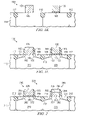
- FIGS. 1A to 1L illustrate sectional views of selected steps in a method of manufacturing a semiconductor device 100 , according to the principles of the present invention.
- the method includes forming a gate dielectric 105 over a substrate 110 .
- the method also includes depositing a mold layer 115 having a first opening 120 therein over the gate dielectric 105 .
- the method also includes creating a first metal gate electrode 125 , by depositing a first metal in the first opening 120 .
- creating a first metal gate electrode 125 further includes removing excess first metal 130 on the mold layer 115 and not in the first opening 120 , to yield the structure shown in FIG. 1D .
- FIGS. 1E to 1G illustrate one preferred embodiment of the method that further includes creating a second metal gate electrode 135 over the substrate 110 .
- a second opening 140 is formed in the mold layer 115 .
- the method continues, as shown in FIG. 1F , by depositing a second metal in the second opening 140 to form the second metal gate electrode 135 .
- creating a second metal gate further includes removing excess second metal 145 on the mold layer 115 , and not in the second opening 140 , to yield the structure shown in FIG. 1G .
- FIGS. 1H to 1J illustrate an alternative preferred embodiment of the method to create the second metal gate electrode 135 over the substrate 110 .
- the mold layer 115 illustrated in FIG. 1D is substantially removed and, as illustrated in FIG. 1H , a second mold layer 150 having the second opening 140 therein, is formed over the gate dielectric 105 .
- the second metal gate electrode 135 is created by depositing a second metal in the second opening 140 . Similar to that discussed above, in certain embodiments, excess second metal 145 on the second mold layer 150 and not in the second opening 140 is removed to yield the structure shown in FIG. 1J .
- FIGS. 1K to 1L The exemplary method continues as shown in FIGS. 1K to 1L , with the fabrication of other semiconductor device components.
- certain embodiments include removing portions of the first mold layer 115 ( FIG. 1G ) or second mold layer 150 ( FIG. 1J ), as well as portions of the gate dielectric layer 105 not under the first and second metal gate electrodes 125 , 135 .
- portions of the first or second mold layer 115 , 150 can be retained to serve as part of an interconnect structure.
- certain embodiments of the method further include implanting dopants, with the metal gate electrodes 125 , 135 , serving as masks to facilitate forming source and drain structures 155 , 160 , and lightly doped drain regions 162 , that are self-aligned with the first and second metal electrodes 125 , 135 .
- FIG. 1L also illustrates forming sidewalls 165 adjacent to the first and second metals electrodes 125 , 135 .
- Other embodiments of the method further include, as illustrated in FIG. 1L , the formation of NMOS and PMOS tubs, 170 , 175 .
- the substrate 110 and gate dielectric 105 can be any conventional materials suitable for use in semiconductor device manufacturing, such silicon and silicon dioxide or silicon oxynitride, respectively.
- the gate dielectric 105 is a high dielectric constant material (e.g., a material having a higher dielectric constant than silicon dioxide), such as hafnium dioxide, hafnium silicate, hafnium silicon oxynitride or similar materials well known to those skilled in the art.
- the materials serving as the mold layers 115 , 150 are selected based on one or more desirable characteristics.
- CMP chemical mechanical polishing
- the mold layers 115 , 150 are formed using conventional techniques, such as spin coating, to deposit a resist material over the substrate.
- the resist material may be any number of energy sensitive materials, well known to those skilled in the art, that can be patterned upon exposure to radiation, as further discussed below.
- suitable resist materials include polymethyl methacrylate, phenolic resin matrix and diazonaphthoquinone, poly cis-isoprene resin matrix and bisazide, phenol-formaldehyde copolymer and diazoquinone, polybutene-1-sulfone, glycidyl methacrylate and ethyl acrylate or similar compounds well known to those skilled in the art.
- the mold layers 115 , 150 are composed of materials that can be easily removed with high selectivity over the gate insulating layer or the deposited metal and generally has a low dielectric constant (e.g., a low-k material having a dielectric constant less than silicon dioxide).
- Suitable materials include organic polymers, such as hydrogen silsesquioxane or methyl silsesquioxane. Such compounds are also favored because they have acceptable mechanical stability.
- the mold layers 115 , 150 are composed of an inorganic material having high mechanical stability such as silicon dioxide, silicon oxide aerogel, silicon oxyfluoride or silicon nitride.
- the mold layer 115 and second mold layer 150 have different chemical compositions. In other preferred embodiments, however, the mold layer 115 and second mold layer 150 have substantially the same chemical composition.
- the mold layer 115 and second mold layer 150 can be formed over the substrate 110 using any number of conventional procedures, including chemical vapor deposition (CVD), physical vapor deposition (PVD), plasma enhanced CVD (PECVD), atomic layer deposition (ALD), spin coating, or other producers well known to those skilled in the art.
- CVD chemical vapor deposition
- PVD physical vapor deposition
- PECVD plasma enhanced CVD
- ALD atomic layer deposition
- spin coating or other producers well known to those skilled in the art.
- any number of conventional techniques can be used to pattern and etch the mold layers 115 , 150 to form openings 120 , 140 suitable for depositing the metals to thereby form metal gate electrodes 125 , 135 .
- Such techniques include lithographic processes commonly used to fabricate devices such as integrated circuit devices, optical devices, micro-electromechanical (MEMS) devices, etc . . . .
- MEMS micro-electromechanical
- a pattern is defined and developed in an energy sensitive material.
- the pattern is then used as an etch mask to transfer the pattern into a layer of material underlying the energy sensitive material serving as the mold layer 115 , 150 .
- the pattern is typically transferred into a mold layer 115 , 150 formed over the substrate.
- Any number of radiation sources including visible and ultraviolet light, x-rays, ion beam, or electron beam radiation, can be used in to facilitate pattern transfer.
- the first and second metal gate electrodes 125 , 135 are created, it is desirable to substantially remove the entire mold layer 115 , or in some embodiments, the second mold layer 150 , before forming other components of the semiconductor device 100 .
- any number of conventional damascene procedures may be used to deposit first or second metals in the openings 120 , 140 .
- the openings 120 , 140 may be filled, for example, via physical and chemical vapor deposition.
- atomic layer deposition and electrochemical deposition are preferred because these techniques provide more uniform filling of the openings 120 , 140 .
- the first and second metal gate electrodes 125 , 135 have different work functions, corresponding to the work functions used in conventional NMOS and PMOS devices, respectively.
- the first metal is an n + metal having a work function between about 4 and about 4.2 eV
- the second metal is a p + metal having a work function between about 5 and about 5.2 eV.
- first metals having a work function between about 4 and about 4.2 eV include titanium, chromium, manganese, zirconium, tantalum; tantalum nitride, and mixtures thereof including alloys, nitrides and silicides.
- the first metal is refractory metal, such as tantalum or tantalum nitride. Refractory metals are preferred because these metals remain chemically and structurally stable throughout subsequent transistor component fabrication steps, such as dopant implantation or thermal anneals.
- suitable second metals having a work function between about 5 and about 5.2 eV include cobalt, nickel, molybdenum, ruthenium, rhodium, palladium, rhenium, iridium, platinum, gold, and mixtures thereof including alloys, nitrides and silicides.
- the second metal is molybdenum or platinum, because these metals remain chemically and structurally stable throughout subsequent transistor component fabrication steps.
- the deposition of the first or second metal into the openings results in the deposition of excess metal 130 , 145 on remaining portions of the mold layers 115 or second mold layer 150 .
- the excess metal 130 , 145 is removed by chemical mechanical polishing (CMP).
- CMP chemical mechanical polishing
- the excess metal 130 , 145 is removed by dry etching in fluorine or chlorine based chemistries.
- FIG. 2 illustrates a sectional view of an embodiment of an active device 200 .
- the active device 200 shown in FIG. 2 is produced by a process that includes forming a gate dielectric 205 over a substrate 210 and depositing a mold layer 115 having a first opening 120 therein over the gate dielectric 205 . Also included in the process is the creation of a first metal gate electrode 225 by depositing a first metal in the first opening 120 .
- the active device 200 is produced by processes that further include creating a second metal gate electrode 235 over the substrate 210 by forming a second opening 140 in the mold layer 115 and depositing a second metal in the second opening 140 .
- the active device 200 is produced by processes that further includes creating a second metal gate electrode 245 over the substrate 210 by removing the mold layer 115 and forming second mold layer 150 having the second opening therein 140 and depositing the second metal in the second opening 140 .
- Certain preferred embodiments of the active device 200 further include source drain and lightly doped regions 255 , 260 , 262 , sidewalls 265 formed adjacent to the first and second metal gate electrodes 225 , 235 , as well as NMOS and PMOS tubs 270 , 275 and isolation structures 212 .
- a doped polysilicon layer 295 may be deposited on one or both of the first and second metal electrodes 225 , 235 to form a gate stack.
- the first metal gate electrode 225 has a work function between about 4.0 and about 4.2 eV and the second metal gate electrode 235 has a work function between about 5.0 and about 5.2 eV.
- the active device 200 is a CMOS device that including an NMOS transistor 285 having the first metal gate electrode 225 and a PMOS transistor 290 having the second metal gate electrode 235 .
- FIGS. 3A to 3B presents sectional views of a method for manufacturing an integrated circuit 300 according to the principles of the present invention.
- the method of manufacturing includes forming active devices 310 , 315 having dual work function metal gate electrodes 320 over or in a semiconductor substrate 330 . Any of the above-described processes can be used to form the active devices 310 , 315 .
- FIG. 3B shows forming interconnect metals lines 340 in or on one or more insulating layer 350 located over the active devices 310 , 315 .
- the method may further be extended to form any number of additional interconnects 340 and would also understand how to connect those interconnects 340 with the active devices 310 , 315 to form an operative integrated circuit 300 .
Abstract
The present invention provides, in one embodiment, a method (100) of forming dual work function metal gate electrodes in a semiconductor device. The method includes forming a gate dielectric (105) over a substrate (110) and depositing a mold layer (115) having a first opening (120) therein over the gate dielectric (105). The method further includes creating a first metal gate electrode (125) by depositing a first metal in the first opening (120). Other embodiments include an active device (200) produced by the above-described method and method of manufacturing an integrated circuit (300) using the above-described method.
Description
The present invention is directed in general to semiconductor devices and the manufacture of semiconductor devices and, more specifically, to manufacturing dual work function metal gate structures for semiconductor devices.
The ability to dope polysilicon gates to different degrees allows one to adjust the work function of gate electrode materials to particular types of complementary metal oxide silicon (CMOS) transistors. It is desirable to adjust the work function of a gate electrode to be close to either the conduction band or the valence band of silicon, because this reduces the threshold voltage of the transistor, thereby facilitating a high drive current. For instance, dual work function gates are advantageously used in semiconductor devices having both PMOS and NMOS transistors. The use of doped polysilicon gates becomes problematic, however, as the dimensions of gates and gate insulators are reduced.
Polysilicon gates can only accommodate a finite amount of dopant. This limitation can result in a depletion of gate charge carriers at the interface between the gate and gate dielectric, when the gate electrode of a device is biased to invert the channel. Consequently, the electrical thickness of the gate dielectric is substantially increased, thereby deteriorating the performance characteristics of the transistor, such as reducing the drive current and switching speed. For instance, the electrical thickness of a gate dielectric in some PMOS transistors can increase from about 1.0 nanometer during accumulation mode, to about 1.8 nanometer during inversion mode.
Metal gates are an attractive alternative to polysilicon because they have a larger supply of charge carriers than doped polysilicon gates. When a metal gate is inverted, there is no substantial depletion of carriers at the interface between the metal gate and gate dielectric. Accordingly, the transistor's performance is not deteriorated because the electrical thickness of the gate stack is not increased. The integration of semiconductor transistors having dual work function metal gates has been troublesome, however.
Ideally, dual work function metal gates should be compatible with conventional gate dielectric materials and have suitably adjustable work functions. Moreover, the fabrication of metal gates should be easily adaptable to conventional semiconductor device fabrication processes. It has proven challenging, however, to simply deposit and etch metals to form gate structures. For instance, it can be difficult to find etchants and etch conditions where gate metals can be etched with high selectively, that is, without damaging the underlying gate insulator and silicon substrate. Additionally, if two different metals are used to provide dual work function gates, a deposit-and-etch fabrication scheme entails the further complications of selectively etching one gate metal over another gate metal, or etching both metal gates simultaneously.
Previous attempts to reduce these difficulties have not been entirely successful. For instance, to protect the gate dielectric when the metal layer is patterned and etched, some manufacturers have proposed depositing an etch barrier layer between the gate dielectric and the metal layers. This process not only adds to the thickness to the gate dielectric, but also involves additional processing steps. To avoid the need to selectively etch one metal over another metal, some have proposed using a single metal, having midrange work function, as the gate material. Unfortunately, transistors having such single-metal gate electrodes have undesirably high threshold voltages.
Others have proposed a gate-last fabrication scheme. First, a conventional transistor is fully manufactured, including the fabrication of a polysilicon gate and with underlying doped regions implanted. The polysilicon gate and underlying gate dielectric are then removed to provide a gate opening. A new gate dielectric is then conformally deposited on the sides and bottom of the gate opening, followed by filling the gate opening with a metal, to replace the polysilicon gate. In addition to having extra processing steps, such gate-last fabrication schemes have a number of limitations.
In a gate-last fabrication schemes, dopants are implanted into various components of the transistor, such as the source and drain, before the new gate dielectric and replacing metal gate is formed. It follows, therefore, that gate-last fabrication schemes require that all subsequent steps to depositing the gate metal and gate dielectric are done at low temperatures (e.g., below about 700° C.) to prevent the diffusion of dopants. Low temperature processing is undesirable because high temperature anneals are done to improve the quality of the gate dielectric.
In addition, transistors manufactured using gate-last fabrication schemes are more prone to fringe-induced barrier lowering (FIBL). As well known by those skilled in the art, FIBL involves increased coupling between the source and the gate electrode due to the presence of insulating material with a high dielectric constant on the sides of the gate opening. This, in turn, can cause barrier lowering, resulting in transistors with undesirably high leakage current.
There is also a problem with the alignment of source and drain structures when using a gate-last fabrication scheme. When the conventional transistor is manufactured, the polysilicon gate is used as a mask to allow precise definition of the source/drain regions and alignment with the polysilicon gate. Such self-aligned structures minimize overlap between the gate and source and drain and thereby advantageously improve transistor performance reducing the capacitance between the gate and source drain structure.
Self-alignment is lost, however, when the polysilicon gate is replaced by the metal gate in a replacement gate flow. The metal gate does not have the same dimensions as the polysilicon gate because procedures to remove polysilicon can also remove portions of gate sidewall material. The presence of gate insulating material on the sides of the gate opening also contributes to the replacing metal gate having a different size than the polysilicon gate.
Accordingly, what is needed in the art is a method of manufacturing semiconductor devices having dual work function metal electrodes, while not introducing additional problems into semiconductor device manufacturing processes.
To address the above-discussed deficiencies of the prior art, one embodiment is directed to a method of forming dual work function metal gate electrodes in a semiconductor device. The method includes forming a gate dielectric over a substrate and depositing a mold layer having a first opening therein over the gate dielectric. The method further includes creating a first metal gate electrode by depositing a first metal in the first opening.
Another embodiment provides a method of manufacturing an integrated circuit. The method comprises using the above-described method to form active devices having dual work function metal gate electrodes over or in a semiconductor substrate. The method further includes forming interconnect metal lines on one of more insulating layers located over the active devices. The method also includes connecting the interconnects with the active devices to form an operative integrated circuit. Yet another embodiment is an active device produced by the above-describe method of forming dual work function metal gate electrodes.
The foregoing has outlined preferred and alternative features of the present invention so that those of ordinary skill in the art may better understand the detailed description of the invention that follows. Additional features of the invention described hereinafter can also form the subject of the claims of the invention. Those skilled in the art should appreciate that they can readily use the disclosed conception and specific embodiment as a basis for designing or modifying other structures for carrying out the same purposes of the present invention. Those skilled in the art should also realize that such equivalent constructions do not depart from the scope of the invention.
The invention is best understood from the following detailed description when read with the accompanying FIGUREs. It is emphasized that in accordance with the standard practice in the semiconductor industry, various features may not be drawn to scale. In fact, the dimensions of the various features may be arbitrarily increased or reduced for clarity of discussion. Reference is now made to the following descriptions taken in conjunction with the accompanying drawings, in which:
The present invention recognizes the advantageous use of a gate-first fabrication scheme for manufacturing dual work function metal gate electrodes in semiconducting devices. Forming the dual work function metal gate electrodes as an early step in device manufacturing provides several benefits. The underlying gate insulating layer can be subjected to high temperature anneals to improve its functional properties, before implanting dopants into various components of the device. Moreover, the metal gate can be used as a mask so that dopants implanted to form source and drain structures are self-aligned with the gate.
One embodiment of the present invention is a method of manufacturing a semiconductor device. FIGS. 1A to 1L illustrate sectional views of selected steps in a method of manufacturing a semiconductor device 100, according to the principles of the present invention. Turning to FIG. 1A , the method includes forming a gate dielectric 105 over a substrate 110. In some embodiments, it is advantageous to form isolation structures 112, via shallow trench isolation. As well understood by those skilled in the art, however, isolation structures 112 could be formed at any number of stages in the method.
As further illustrated in FIG. 1B , the method also includes depositing a mold layer 115 having a first opening 120 therein over the gate dielectric 105. As shown in FIG. 1C , the method also includes creating a first metal gate electrode 125, by depositing a first metal in the first opening 120. In some preferred embodiments, creating a first metal gate electrode 125 further includes removing excess first metal 130 on the mold layer 115 and not in the first opening 120, to yield the structure shown in FIG. 1D .
The exemplary method continues as shown in FIGS. 1K to 1L , with the fabrication of other semiconductor device components. As shown in FIG. 1K , certain embodiments include removing portions of the first mold layer 115 (FIG. 1G ) or second mold layer 150 (FIG. 1J ), as well as portions of the gate dielectric layer 105 not under the first and second metal gate electrodes 125, 135. As further discussed below, in other embodiments, however, portions of the first or second mold layer 115, 150 can be retained to serve as part of an interconnect structure.
As presented in FIG. 1L , certain embodiments of the method further include implanting dopants, with the metal gate electrodes 125, 135, serving as masks to facilitate forming source and drain structures 155, 160, and lightly doped drain regions 162, that are self-aligned with the first and second metal electrodes 125, 135. FIG. 1L also illustrates forming sidewalls 165 adjacent to the first and second metals electrodes 125, 135. Other embodiments of the method further include, as illustrated in FIG. 1L , the formation of NMOS and PMOS tubs, 170, 175.
With continuing reference to FIGS. 1A–1L , the substrate 110 and gate dielectric 105 can be any conventional materials suitable for use in semiconductor device manufacturing, such silicon and silicon dioxide or silicon oxynitride, respectively. In certain preferred embodiments, the gate dielectric 105 is a high dielectric constant material (e.g., a material having a higher dielectric constant than silicon dioxide), such as hafnium dioxide, hafnium silicate, hafnium silicon oxynitride or similar materials well known to those skilled in the art.
The materials serving as the mold layers 115, 150 are selected based on one or more desirable characteristics. In some embodiments, it is preferable for the mold layer material to be easily patterned, as further discussed below, and to have high temperature stability (e.g., melting or decomposition point above about 425° C.). In such embodiments, it is also desirable for the mold layers 115, 150 to have sufficient mechanical stability so as to remain intact when chemical mechanical polishing (CMP) or etching is performed to remove excess metal, 130, 145.
In certain embodiments, the mold layers 115, 150 are formed using conventional techniques, such as spin coating, to deposit a resist material over the substrate. The resist material may be any number of energy sensitive materials, well known to those skilled in the art, that can be patterned upon exposure to radiation, as further discussed below. Examples of suitable resist materials include polymethyl methacrylate, phenolic resin matrix and diazonaphthoquinone, poly cis-isoprene resin matrix and bisazide, phenol-formaldehyde copolymer and diazoquinone, polybutene-1-sulfone, glycidyl methacrylate and ethyl acrylate or similar compounds well known to those skilled in the art.
In other embodiments, the mold layers 115, 150 are composed of materials that can be easily removed with high selectivity over the gate insulating layer or the deposited metal and generally has a low dielectric constant (e.g., a low-k material having a dielectric constant less than silicon dioxide). Suitable materials include organic polymers, such as hydrogen silsesquioxane or methyl silsesquioxane. Such compounds are also favored because they have acceptable mechanical stability.
In still other embodiments, the mold layers 115, 150 are composed of an inorganic material having high mechanical stability such as silicon dioxide, silicon oxide aerogel, silicon oxyfluoride or silicon nitride. In some embodiments, the mold layer 115 and second mold layer 150 have different chemical compositions. In other preferred embodiments, however, the mold layer 115 and second mold layer 150 have substantially the same chemical composition. The mold layer 115 and second mold layer 150 can be formed over the substrate 110 using any number of conventional procedures, including chemical vapor deposition (CVD), physical vapor deposition (PVD), plasma enhanced CVD (PECVD), atomic layer deposition (ALD), spin coating, or other producers well known to those skilled in the art.
Any number of conventional techniques can be used to pattern and etch the mold layers 115, 150 to form openings 120, 140 suitable for depositing the metals to thereby form metal gate electrodes 125, 135. Such techniques include lithographic processes commonly used to fabricate devices such as integrated circuit devices, optical devices, micro-electromechanical (MEMS) devices, etc . . . . In a typical lithographic process, a pattern is defined and developed in an energy sensitive material. The pattern is then used as an etch mask to transfer the pattern into a layer of material underlying the energy sensitive material serving as the mold layer 115, 150. In semiconductor device fabrication, the pattern is typically transferred into a mold layer 115, 150 formed over the substrate. Any number of radiation sources, including visible and ultraviolet light, x-rays, ion beam, or electron beam radiation, can be used in to facilitate pattern transfer.
As noted above, in some embodiments, after the first and second metal gate electrodes 125, 135 are created, it is desirable to substantially remove the entire mold layer 115, or in some embodiments, the second mold layer 150, before forming other components of the semiconductor device 100.
Any number of conventional damascene procedures may be used to deposit first or second metals in the openings 120, 140. The openings 120, 140 may be filled, for example, via physical and chemical vapor deposition. In particular, atomic layer deposition and electrochemical deposition are preferred because these techniques provide more uniform filling of the openings 120, 140.
In certain preferred embodiments the first and second metal gate electrodes 125, 135 have different work functions, corresponding to the work functions used in conventional NMOS and PMOS devices, respectively. In some embodiments, for example, the first metal is an n+ metal having a work function between about 4 and about 4.2 eV, while the second metal is a p+ metal having a work function between about 5 and about 5.2 eV.
Examples of suitable first metals having a work function between about 4 and about 4.2 eV include titanium, chromium, manganese, zirconium, tantalum; tantalum nitride, and mixtures thereof including alloys, nitrides and silicides. In certain preferred embodiments, the first metal is refractory metal, such as tantalum or tantalum nitride. Refractory metals are preferred because these metals remain chemically and structurally stable throughout subsequent transistor component fabrication steps, such as dopant implantation or thermal anneals.
Examples of suitable second metals having a work function between about 5 and about 5.2 eV include cobalt, nickel, molybdenum, ruthenium, rhodium, palladium, rhenium, iridium, platinum, gold, and mixtures thereof including alloys, nitrides and silicides. In certain preferred embodiments, the second metal is molybdenum or platinum, because these metals remain chemically and structurally stable throughout subsequent transistor component fabrication steps.
As noted above, in certain embodiments, the deposition of the first or second metal into the openings results in the deposition of excess metal 130, 145 on remaining portions of the mold layers 115 or second mold layer 150. In such embodiments, it is desirable to selectively remove portions of the excess metal that are above the mold layers 115, 150 but not inside the opening 120, 140. In some embodiments, for example, the excess metal 130, 145 is removed by chemical mechanical polishing (CMP). In other embodiments, the excess metal 130, 145 is removed by dry etching in fluorine or chlorine based chemistries.
Yet another embodiment of the present invention, is an active device 200 produced by the processes described above and illustrated in FIGS. 1A to 1L . FIG. 2 illustrates a sectional view of an embodiment of an active device 200. Like reference numbers are used to depict structures analogous to that shown in FIGS. 1A to 1L . With continuing reference to FIGS. 1A to 1L , the active device 200 shown in FIG. 2 is produced by a process that includes forming a gate dielectric 205 over a substrate 210 and depositing a mold layer 115 having a first opening 120 therein over the gate dielectric 205. Also included in the process is the creation of a first metal gate electrode 225 by depositing a first metal in the first opening 120.
In some preferred embodiments the active device 200 is produced by processes that further include creating a second metal gate electrode 235 over the substrate 210 by forming a second opening 140 in the mold layer 115 and depositing a second metal in the second opening 140. In alternative embodiments, however, the active device 200 is produced by processes that further includes creating a second metal gate electrode 245 over the substrate 210 by removing the mold layer 115 and forming second mold layer 150 having the second opening therein 140 and depositing the second metal in the second opening 140.
Certain preferred embodiments of the active device 200 further include source drain and lightly doped regions 255, 260, 262, sidewalls 265 formed adjacent to the first and second metal gate electrodes 225, 235, as well as NMOS and PMOS tubs 270, 275 and isolation structures 212. In addition, as shown in FIG. 2 a doped polysilicon layer 295 may be deposited on one or both of the first and second metal electrodes 225, 235 to form a gate stack.
In some preferred embodiments of the active device 200, the first metal gate electrode 225 has a work function between about 4.0 and about 4.2 eV and the second metal gate electrode 235 has a work function between about 5.0 and about 5.2 eV. In yet other preferred embodiments, the active device 200 is a CMOS device that including an NMOS transistor 285 having the first metal gate electrode 225 and a PMOS transistor 290 having the second metal gate electrode 235.
Yet another embodiment of the present invention is a method of manufacturing an integrated circuit. FIGS. 3A to 3B presents sectional views of a method for manufacturing an integrated circuit 300 according to the principles of the present invention. Turning to FIG. 3A , the method of manufacturing includes forming active devices 310, 315 having dual work function metal gate electrodes 320 over or in a semiconductor substrate 330. Any of the above-described processes can be used to form the active devices 310, 315. FIG. 3B shows forming interconnect metals lines 340 in or on one or more insulating layer 350 located over the active devices 310, 315. One of ordinary skill would understand that the method may further be extended to form any number of additional interconnects 340 and would also understand how to connect those interconnects 340 with the active devices 310, 315 to form an operative integrated circuit 300.
Although the present invention has been described in detail, one of ordinary skill in the art should understand that they can make various changes, substitutions and alterations herein without departing from the scope of the invention.
Claims (6)
1. A method of forming dual work function metal gate electrodes in a semiconductor device, comprising:
forming a gate dielectric over a substrate;
depositing a first mold layer over said gate dielectric;
etching said first mold layer to create a first opening;
creating a first metal gate electrode by depositing a first metal in said first opening;
removing said first mold layer;
forming a second mold layer;
then, etching said second mold layer to create a second opening; and
depositing a second metal in said second opening.
2. The method as recited in claim 1 , wherein first and second mold layers have different chemical compositions.
3. The method as recited in claim 1 , wherein said mold layer is selected from the group consisting of
a resist material;
an organic polymer; and
an inorganic material.
4. The method as recited in claim 1 , wherein said first metal has a work function between about 4 and about 4.2 eV and said second metal has a work function between about 5 and about 5.2 eV.
5. The method as recited in claim 1 , wherein said first metal is selected from the group consisting of:
titanium;
chromium;
manganese;
zirconium;
tantalum;
tantalum nitride; and
mixtures thereof.
6. The method as recited in claim 1 , wherein said first metal is selected from the group consisting of:
cobalt;
nickel;
molybdenum;
ruthenium;
rhodium;
palladium;
rhenium;
iridium;
platinum;
gold; and
mixtures thereof.
Priority Applications (1)
| Application Number | Priority Date | Filing Date | Title |
|---|---|---|---|
| US10/649,425 US7005365B2 (en) | 2003-08-27 | 2003-08-27 | Structure and method to fabricate self-aligned transistors with dual work function metal gate electrodes |
Applications Claiming Priority (1)
| Application Number | Priority Date | Filing Date | Title |
|---|---|---|---|
| US10/649,425 US7005365B2 (en) | 2003-08-27 | 2003-08-27 | Structure and method to fabricate self-aligned transistors with dual work function metal gate electrodes |
Publications (2)
| Publication Number | Publication Date |
|---|---|
| US20050045923A1 US20050045923A1 (en) | 2005-03-03 |
| US7005365B2 true US7005365B2 (en) | 2006-02-28 |
Family
ID=34216942
Family Applications (1)
| Application Number | Title | Priority Date | Filing Date |
|---|---|---|---|
| US10/649,425 Expired - Lifetime US7005365B2 (en) | 2003-08-27 | 2003-08-27 | Structure and method to fabricate self-aligned transistors with dual work function metal gate electrodes |
Country Status (1)
| Country | Link |
|---|---|
| US (1) | US7005365B2 (en) |
Cited By (10)
| Publication number | Priority date | Publication date | Assignee | Title |
|---|---|---|---|---|
| US20050145893A1 (en) * | 2003-12-29 | 2005-07-07 | Doczy Mark L. | Methods for fabricating metal gate structures |
| US20050258468A1 (en) * | 2004-05-24 | 2005-11-24 | Texas Instruments, Incorporated | Dual work function metal gate integration in semiconductor devices |
| US20070108529A1 (en) * | 2005-11-14 | 2007-05-17 | Taiwan Semiconductor Manufacturing Company, Ltd. | Strained gate electrodes in semiconductor devices |
| US20080203485A1 (en) * | 2007-02-28 | 2008-08-28 | International Business Machines Corporation | Strained metal gate structure for cmos devices with improved channel mobility and methods of forming the same |
| US20090095991A1 (en) * | 2007-10-11 | 2009-04-16 | International Business Machines Corporation | Method of forming strained mosfet devices using phase transformable materials |
| US20100052067A1 (en) * | 2008-08-27 | 2010-03-04 | Taiwan Semiconductor Manufacturing Company, Ltd. | Method of fabricating dual high-k metal gates for mos devices |
| US20100081262A1 (en) * | 2008-09-26 | 2010-04-01 | Taiwan Semiconductor Manufacturing Company, Ltd. | Method for forming metal gates in a gate last process |
| US20100087055A1 (en) * | 2008-10-06 | 2010-04-08 | Taiwan Semiconductor Manufacturing Company, Ltd. | Method for gate height control in a gate last process |
| US8569135B2 (en) | 2011-07-20 | 2013-10-29 | International Business Machines Corporation | Replacement gate electrode with planar work function material layers |
| TWI419264B (en) * | 2008-11-14 | 2013-12-11 | Taiwan Semiconductor Mfg | Method for fabricating semiconductor device |
Families Citing this family (4)
| Publication number | Priority date | Publication date | Assignee | Title |
|---|---|---|---|---|
| US7030001B2 (en) * | 2004-04-19 | 2006-04-18 | Freescale Semiconductor, Inc. | Method for forming a gate electrode having a metal |
| US7799668B2 (en) * | 2005-08-17 | 2010-09-21 | Texas Instruments Incorporated | Formation of uniform silicate gate dielectrics |
| DE102008006961A1 (en) * | 2008-01-31 | 2009-08-27 | Advanced Micro Devices, Inc., Sunnyvale | A method of creating a deformed channel region in a transistor by deep implantation of a strain inducing species under the channel region |
| US10157990B2 (en) * | 2016-12-08 | 2018-12-18 | Taiwan Semiconductor Manufacturing Co., Ltd. | Semiconductor device with capping structure and method of forming the same |
Citations (6)
| Publication number | Priority date | Publication date | Assignee | Title |
|---|---|---|---|---|
| GB2347789A (en) | 1999-03-01 | 2000-09-13 | Nec Corp | Complementary integrated circuit |
| US6130123A (en) * | 1998-06-30 | 2000-10-10 | Intel Corporation | Method for making a complementary metal gate electrode technology |
| US6383879B1 (en) | 1999-12-03 | 2002-05-07 | Agere Systems Guardian Corp. | Semiconductor device having a metal gate with a work function compatible with a semiconductor device |
| US6397861B1 (en) | 1998-08-11 | 2002-06-04 | Novellus Systems, Inc. | Situ plasma clean gas injection |
| US6534423B1 (en) | 2000-12-27 | 2003-03-18 | Novellus Systems, Inc. | Use of inductively-coupled plasma in plasma-enhanced chemical vapor deposition reactor to improve film-to-wall adhesion following in-situ plasma clean |
| US6583012B1 (en) * | 2001-02-13 | 2003-06-24 | Advanced Micro Devices, Inc. | Semiconductor devices utilizing differently composed metal-based in-laid gate electrodes |
-
2003
- 2003-08-27 US US10/649,425 patent/US7005365B2/en not_active Expired - Lifetime
Patent Citations (7)
| Publication number | Priority date | Publication date | Assignee | Title |
|---|---|---|---|---|
| US6130123A (en) * | 1998-06-30 | 2000-10-10 | Intel Corporation | Method for making a complementary metal gate electrode technology |
| US6397861B1 (en) | 1998-08-11 | 2002-06-04 | Novellus Systems, Inc. | Situ plasma clean gas injection |
| GB2347789A (en) | 1999-03-01 | 2000-09-13 | Nec Corp | Complementary integrated circuit |
| US20040080001A1 (en) * | 1999-03-01 | 2004-04-29 | Kiyoshi Takeuchi | Complementary integrated circuit and method of manufacturing same |
| US6383879B1 (en) | 1999-12-03 | 2002-05-07 | Agere Systems Guardian Corp. | Semiconductor device having a metal gate with a work function compatible with a semiconductor device |
| US6534423B1 (en) | 2000-12-27 | 2003-03-18 | Novellus Systems, Inc. | Use of inductively-coupled plasma in plasma-enhanced chemical vapor deposition reactor to improve film-to-wall adhesion following in-situ plasma clean |
| US6583012B1 (en) * | 2001-02-13 | 2003-06-24 | Advanced Micro Devices, Inc. | Semiconductor devices utilizing differently composed metal-based in-laid gate electrodes |
Non-Patent Citations (2)
| Title |
|---|
| "Pursuing the Perfect Low-K Dielectric"; www.e-insite.net/semiconductor/index.asp?layout=articlePrint&article ID=CA164243. |
| B. Maiti and P.J. Tobin; "Metal Gates for Advanced CMOS Technology"; SPIE vol. 3881; Sep. 1999; pp. 46-57. |
Cited By (20)
| Publication number | Priority date | Publication date | Assignee | Title |
|---|---|---|---|---|
| US20050145893A1 (en) * | 2003-12-29 | 2005-07-07 | Doczy Mark L. | Methods for fabricating metal gate structures |
| US20050202644A1 (en) * | 2003-12-29 | 2005-09-15 | Doczy Mark L. | Method for fabricating metal gate structures |
| US7439571B2 (en) | 2003-12-29 | 2008-10-21 | Intel Corporation | Method for fabricating metal gate structures |
| US20050258468A1 (en) * | 2004-05-24 | 2005-11-24 | Texas Instruments, Incorporated | Dual work function metal gate integration in semiconductor devices |
| US7528024B2 (en) * | 2004-05-24 | 2009-05-05 | Texas Instruments Incorporated | Dual work function metal gate integration in semiconductor devices |
| US20070108529A1 (en) * | 2005-11-14 | 2007-05-17 | Taiwan Semiconductor Manufacturing Company, Ltd. | Strained gate electrodes in semiconductor devices |
| US8835291B2 (en) | 2005-11-14 | 2014-09-16 | Taiwan Semiconductor Manufacturing Company, Ltd. | Strained gate electrodes in semiconductor devices |
| US20080203485A1 (en) * | 2007-02-28 | 2008-08-28 | International Business Machines Corporation | Strained metal gate structure for cmos devices with improved channel mobility and methods of forming the same |
| US20090095991A1 (en) * | 2007-10-11 | 2009-04-16 | International Business Machines Corporation | Method of forming strained mosfet devices using phase transformable materials |
| US20100052067A1 (en) * | 2008-08-27 | 2010-03-04 | Taiwan Semiconductor Manufacturing Company, Ltd. | Method of fabricating dual high-k metal gates for mos devices |
| US9263445B2 (en) | 2008-08-27 | 2016-02-16 | Taiwan Semiconductor Manufacturing Company, Ltd. | Method of fabricating dual high-k metal gates for MOS devices |
| US8105931B2 (en) | 2008-08-27 | 2012-01-31 | Taiwan Semiconductor Manufacturing Company, Ltd. | Method of fabricating dual high-k metal gates for MOS devices |
| US8853068B2 (en) | 2008-08-27 | 2014-10-07 | Taiwan Semiconductor Manufacturing Company, Ltd. | Method of fabricating dual high-k metal gate for MOS devices |
| US20100081262A1 (en) * | 2008-09-26 | 2010-04-01 | Taiwan Semiconductor Manufacturing Company, Ltd. | Method for forming metal gates in a gate last process |
| US7871915B2 (en) | 2008-09-26 | 2011-01-18 | Taiwan Semiconductor Manufacturing Company, Ltd. | Method for forming metal gates in a gate last process |
| US20100087055A1 (en) * | 2008-10-06 | 2010-04-08 | Taiwan Semiconductor Manufacturing Company, Ltd. | Method for gate height control in a gate last process |
| US7977181B2 (en) | 2008-10-06 | 2011-07-12 | Taiwan Semiconductor Manufacturing Company, Ltd. | Method for gate height control in a gate last process |
| TWI419264B (en) * | 2008-11-14 | 2013-12-11 | Taiwan Semiconductor Mfg | Method for fabricating semiconductor device |
| US8853788B2 (en) | 2011-07-20 | 2014-10-07 | International Business Machines Corporation | Replacement gate electrode with planar work function material layers |
| US8569135B2 (en) | 2011-07-20 | 2013-10-29 | International Business Machines Corporation | Replacement gate electrode with planar work function material layers |
Also Published As
| Publication number | Publication date |
|---|---|
| US20050045923A1 (en) | 2005-03-03 |
Similar Documents
| Publication | Publication Date | Title |
|---|---|---|
| US8586404B2 (en) | Method for reducing contact resistance of CMOS image sensor | |
| US7410854B2 (en) | Method of making FUSI gate and resulting structure | |
| US7229873B2 (en) | Process for manufacturing dual work function metal gates in a microelectronics device | |
| TWI382498B (en) | Method for n/p patterning in a gate last process | |
| TWI393219B (en) | Method for gate height control in a gate last process | |
| US7528024B2 (en) | Dual work function metal gate integration in semiconductor devices | |
| CN101789397B (en) | A method of fabricating a semiconductor device | |
| US9437593B2 (en) | Silicided semiconductor structure and method of forming the same | |
| US6800530B2 (en) | Triple layer hard mask for gate patterning to fabricate scaled CMOS transistors | |
| US7005365B2 (en) | Structure and method to fabricate self-aligned transistors with dual work function metal gate electrodes | |
| KR100537580B1 (en) | Process for the fabrication of mosfet devices depletion, silicided source and drain junctions | |
| KR20030058943A (en) | Dual metal gate transistors for CMOS process | |
| JP2007535171A (en) | Dual metal CMOS transistor with adjustable gate electrode work function and fabrication method thereof | |
| KR20040077528A (en) | System and method for integrating multiple metal gates for cmos applications | |
| KR20020077160A (en) | Dual damascene copper gate and interconnet therefore | |
| US6177336B1 (en) | Method for fabricating a metal-oxide semiconductor device | |
| KR100588035B1 (en) | Method of enhanced oxidation of mos transistor gate corners | |
| US7745296B2 (en) | Raised source and drain process with disposable spacers | |
| US8759180B2 (en) | Methods for fabricating step gate electrode structures for field-effect transistors | |
| US9929250B1 (en) | Semiconductor device including optimized gate stack profile | |
| US6995452B2 (en) | MOSFET device with nanoscale channel and method of manufacturing the same | |
| KR20020037942A (en) | Method for manufacturing gate in semiconductor device | |
| KR100398035B1 (en) | Method of manufacturing a transistor in a semiconductor divice | |
| KR20060014001A (en) | Integrated circuit device having a dual-gate structure and method of fabricating the same | |
| KR100573270B1 (en) | Method for fabricating silicide of gate electrode |
Legal Events
| Date | Code | Title | Description |
|---|---|---|---|
| AS | Assignment |
Owner name: TEXAS INSTRUMENTS INCORPORATED, TEXAS Free format text: ASSIGNMENT OF ASSIGNORS INTEREST;ASSIGNOR:CHAMBERS, JAMES J.;REEL/FRAME:014440/0163 Effective date: 20030827 |
|
| STCF | Information on status: patent grant |
Free format text: PATENTED CASE |
|
| FPAY | Fee payment |
Year of fee payment: 4 |
|
| FPAY | Fee payment |
Year of fee payment: 8 |
|
| FPAY | Fee payment |
Year of fee payment: 12 |