US7006393B2 - Method and apparatus for semiconductor device repair with reduced number of programmable elements - Google Patents
Method and apparatus for semiconductor device repair with reduced number of programmable elements Download PDFInfo
- Publication number
- US7006393B2 US7006393B2 US10/862,284 US86228404A US7006393B2 US 7006393 B2 US7006393 B2 US 7006393B2 US 86228404 A US86228404 A US 86228404A US 7006393 B2 US7006393 B2 US 7006393B2
- Authority
- US
- United States
- Prior art keywords
- repair
- address
- group
- nonvolatile
- selection
- Prior art date
- Legal status (The legal status is an assumption and is not a legal conclusion. Google has not performed a legal analysis and makes no representation as to the accuracy of the status listed.)
- Expired - Fee Related
Links
Images


Classifications
-
- G—PHYSICS
- G11—INFORMATION STORAGE
- G11C—STATIC STORES
- G11C29/00—Checking stores for correct operation ; Subsequent repair; Testing stores during standby or offline operation
- G11C29/70—Masking faults in memories by using spares or by reconfiguring
- G11C29/78—Masking faults in memories by using spares or by reconfiguring using programmable devices
- G11C29/80—Masking faults in memories by using spares or by reconfiguring using programmable devices with improved layout
- G11C29/806—Masking faults in memories by using spares or by reconfiguring using programmable devices with improved layout by reducing size of decoders
-
- G—PHYSICS
- G11—INFORMATION STORAGE
- G11C—STATIC STORES
- G11C29/00—Checking stores for correct operation ; Subsequent repair; Testing stores during standby or offline operation
- G11C29/70—Masking faults in memories by using spares or by reconfiguring
- G11C29/78—Masking faults in memories by using spares or by reconfiguring using programmable devices
- G11C29/80—Masking faults in memories by using spares or by reconfiguring using programmable devices with improved layout
- G11C29/81—Masking faults in memories by using spares or by reconfiguring using programmable devices with improved layout using a hierarchical redundancy scheme
Definitions
- This invention relates generally to semiconductor memory circuits, and particularly to circuits and methods for repairing semiconductor memory circuits having redundant memory cells.
- Semiconductor memories generally include a multitude of memory cells arranged in rows and columns. Each memory cell is structured for storing digital information in the form of a “1” or a “0” bit. Many semiconductor memories include extra, i.e., redundant, memory cells that may be substituted for failing memory cells. Semiconductor memories are typically tested after they are fabricated to determine if they contain any failing memory cells (i.e., cells to which bits cannot be dependably written or from which bits cannot be dependably read). Generally, when a semiconductor memory is found to contain failing memory cells, an attempt is made to repair the memory by replacing the failing memory cells with redundant memory cells provided in redundant rows or redundant columns in the semiconductor memory array.
- the failing cell's column address is permanently stored (typically in pre-decoded form) on the chip by programming nonvolatile elements on the chip. Then, during normal operation of the semiconductor memory, if the memory's addressing circuitry receives a memory address, including a column address that corresponds to the column address stored on the chip, redundant circuitry in the memory causes a redundant memory cell in the redundant column to be accessed instead of the memory cell identified by the received memory address. Since every memory cell in the failing cell's column has the same column address, every cell in the failing cell's column, both operative and failing, is replaced by a redundant memory cell in the redundant column. This process for repairing a semiconductor memory using redundant rows and columns is well known in the art.
- a typical semiconductor memory may have many redundant rows and many redundant columns, each redundant block (whether for a row or column) including its own nonvolatile programming elements for enabling and programming the address to which it will respond.
- each redundant block (whether for a row or column) including its own nonvolatile programming elements for enabling and programming the address to which it will respond.
- the density of memory cells on a semiconductor die continues to increase, allowing more memory cells on a semiconductor die, which in turn require more redundant rows and columns to repair the increased number of memory cells.
- an increased number of nonvolatile elements are required to select each redundant row and each redundant column.
- sizes for nonvolatile programming elements have not reduced proportionately to size reduction for memory cells.
- the nonvolatile programming elements take up a larger portion of the available semiconductor die area. In some designs, the nonvolatile programming elements may take up as much as five to ten percent of the overall semiconductor die area.
- the nonvolatile selection element within each group selector may be programmed to generate a selection input signal when the shared address bit is asserted or left unprogrammed to generate a selection input signal when the shared address bit is de-asserted.
- the selection input signals generated by the plurality of group selectors connect to various repair modules such that a match output from a repair module may be generated to select a redundant memory block when the selection input to that repair module is asserted and an address input matches the selected address programmed in that repair module.
- Each repair module may also contain a nonvolatile enable element for enabling that repair module. Additionally, each repair module may also contain a nonvolatile disable element for overriding any programming of the nonvolatile address elements and nonvolatile enable element in that repair module.
- a 0 is used as the shared address bit.
- a group selector connected to eight (i.e., 2 3 ) repair modules may be programmed to generate a selection input when A 0 is de-asserted (i.e., an even address). These eight repair modules may be programmed to different selected addresses resulting in eight repair modules that respond to different even addresses.
- Another group selector connected to four (i.e., 2 2 ) repair modules may be programmed to generate a selection input when A 0 is asserted (i.e., an odd address). These four repair modules may be programmed to different selected addresses resulting in four repair modules that respond to different odd addresses.
- Another embodiment of the present invention includes a plurality of semiconductor memories incorporating the reduced fuse architecture described herein fabricated on a semiconductor wafer.
- FIG. 4 is a block diagram of another exemplary redundancy selection module using nonvolatile enable elements
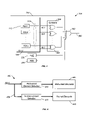
- FIG. 1 is a block diagram of an exemplary memory bank 110 in a semiconductor memory 100 (not shown) in accordance with an embodiment of the present invention.
- a row decode module 120 accepts address inputs 150 for decoding into select signals for each row within a normal memory cell array 140 .
- a column decode module 130 accepts an address input 150 for decoding into select signals for each column within the normal memory cell array 140 .
- At least one row redundancy selection module 200 accepts address inputs 150 for decoding and comparing to selected address 315 (shown in FIG. 4 ) values, such that select signals may be generated for each redundant row within the redundant memory cell array.
- At least one column redundancy selection module 200 accepts address inputs 150 for decoding and comparing to selected address 315 values such that select signals may be generated for each redundant column within the redundant memory cell array. Redundant rows and redundant columns are also referred to herein generically as redundant memory blocks 145 .
- the block diagram shown in FIG. 1 is illustrative of a single memory bank 110 .
- Many modem semiconductor memories are physically organized essentially as a plurality of memory banks 110 organized as a square or rectangle of memory bits such that multiple bits are addressed for each memory address comprised of a combined row and column address.
- the number of bits addressed with each memory address may vary, with exemplary amounts being 4, 8, and 16 bits per memory address.
- a 512 Mbit DRAM may be separated into four banks, each bank containing 128 Mbits.
- Each bank may typically be configured as 8K rows.
- Each bank may typically comprise 16K columns, which may be organized as 4K columns of four bits, 2K columns of eight bits, or 1K columns of 16 bits.
- Typical memory addressing is well known to those skilled in the art, therefore, it is not described in detail herein.
- the arrays of normal memory cells and redundant memory blocks 145 may be segmented into smaller portions to aid in address decoding.
- FIG. 2 is an exemplary embodiment of a redundancy selection module 200 used to select a set of redundant memory blocks 145 .
- Redundancy selection modules for rows and column are typically similar. Therefore, the description of redundancy selection modules 200 applies to both redundant rows and redundant columns unless specified differently herein.
- Each redundancy selection module 200 comprises a plurality of repair modules 300 and a plurality of group selectors 210 .
- An address input 150 bus connects to the repair modules 300 .
- the address input 150 bus may represent all or portions of a row address or a column address.
- At least one of the address bits is designated as a shared address bit 152 , which need not be connected to the repair modules 300 .
- the shared address bit 152 may instead connect to the group selectors 210 .
- FIG. 1 In the embodiment shown in FIG.
- the shared address bit 152 is defined as A 0 .
- any of the bits within the address bus may be used as the shared address bit 152 .
- By using different address bits for different redundant memory blocks 145 it may be possible to increase the overall speed of the entire address input 150 bus.
- Each repair module 300 includes a match output 360 , which may be used to select the redundant memory block 145 corresponding to that repair module 300 in place of the normal memory block containing the faulty memory cell. Additionally, each repair module 300 comprises a set of nonvolatile address elements 312 for programming a selected address 315 , an address comparator 320 , a selection input 310 , a combination element 350 , a nonvolatile enable element 332 , and an optional nonvolatile disable element 334 .
- the address comparator 320 uses individual address bit comparators 322 to compare the address input 150 bus to the selected address 315 programmed into the nonvolatile address elements 312 FZA 1 through FZAn. The bit widths of the address input 150 bus, the nonvolatile address elements 312 , and the address bit comparators 322 may vary with repair modules 300 in different memory architectures, repair modules 300 for redundant rows, and repair modules 300 for redundant columns.
- each repair module 300 may have a nonvolatile disable element 334 used to disable a redundant memory block 145 (not shown).
- the disable function may be needed in a case where a redundant memory block 145 contains a faulty memory bit and should therefore be disabled from use as a redundant memory block 145 .
- the disable function may be needed if a fault or error occurs in the attempt to program a repair module 300 .
- the disable function may override any other nonvolatile element programming within that repair module 300 .
- a nonvolatile enable element 332 within the repair module 300 may be used to control enabling of the repair module 300 if the redundant memory block 145 connected to the repair module 300 is needed. If the nonvolatile enable element 332 is left unprogrammed, the repair module 300 is disabled such that a match output 360 may not be asserted. If the nonvolatile enable element 332 is programmed, the combination element 350 may assert the match output 360 when combined with a matching result from the address comparator 320 and an asserted level on the select signal. When asserted, the match output 360 may select the redundant memory block 145 for operation. In some memory architectures, the match output 360 may be used to select the redundant memory block 145 and deselect the defective memory block.
- the defective memory block may be independently disabled.
- the combination element 350 is shown as a multi-input AND gate and the compare functions as EXCLUSIVE-OR gates to show logical function only, not physical implementation.
- the combination and compare functions may be implemented in many bit widths as well as physical configurations such as, for example, cascaded logic gates, pre-charge and evaluate type implementations, and pre-charge domino type implementations.
- group selectors 210 connect to the selection input 310 of the repair modules 300 .
- the nonvolatile selection elements 219 within the group selectors 210 may be programmed to assert the select signal when the shared address bit 152 is asserted by connecting to the EXCLUSIVE-NOR logic function within the group selector 210 .
- the nonvolatile selection elements 219 within the group selectors 210 may be programmed to assert the select signal when the shared address bit 152 is de-asserted by connecting to an EXCLUSIVE-OR logic function (not shown) rather than the EXCLUSIVE-NOR logic function.
- EXCLUSIVE-OR logic function not shown
- a first additional group selector 212 connects to a first additional repair module 300 ′, and a second additional group selector 214 connects to a second additional repair module 300 ′′. All other group selectors 210 connect to a pair of repair modules 300 .
- This pairing approach is where the savings in number of nonvolatile programming elements is achieved.
- each repair module 300 would contain a nonvolatile programming element for the shared address bit 152 .
- the nonvolatile selection element 219 for controlling the shared address bit 152 is shared between a pair of repair modules 300 . For the example shown in FIG.
- redundancy selection module 200 may also be referred to as a pairs redundancy selection module 200 .
- first additional group selector 212 may typically be used to maintain full reparability for any combination of possible addresses requiring repair.
- the two additional group selectors ( 212 and 214 ) connected to single repair modules ( 300 ′ and 300 ′′) may be eliminated in favor of a group selector 210 connected to a pair of repair modules 300 , saving an additional nonvolatile programming element. This loss of reparability is explained more fully below.
- FIG. 2 is an exemplary embodiment of a redundancy selection module 200 using eight repair modules 300 .
- other numbers are clearly within the scope of this invention, such as, for example only, 16 or 32 repair modules 300 per redundancy selection module 200 .
- the group selectors 210 connect to a varying number of repair modules 300 .
- the variation occurs as a binary sequence. In other words, if the group selectors 210 are considered numbered (with a number N) in a sequence from zero to a maximum number (M), each group selector 210 connects to 2 N repair modules 300 .
- This group selector 210 configuration allows for control of 2 M+ ⁇ 1 (i.e., 1, 3, 7, 15, 31, etc.) repair modules 300 .
- repair modules 300 may be placed in powers of two (i.e., 2, 4, 8, 16, 32, etc.). If needed, a first additional group selector 212 connecting to a single additional repair module 300 may be added to complete control of 2 M+1 repair modules 300 .
- the FIG. 3 embodiment shows four sequentially numbered group selectors 210 designated by numbering the nonvolatile selection elements 219 as FZ 0 through FZ 3 .
- An additional group selector 212 is added resulting in control of a total of 16 repair modules 300 .
- Group selector 0 connects to one (i.e., 2 0 ) repair module 300 .
- Group selector 1 connects to two (i.e., 2 1 ) repair modules 300 .
- Group selector 2 connects to four (i.e., 2 2 ) repair modules 300 .
- Group selector 3 connects to eight (i.e., 2 3 ) repair modules 300 .
- 16 repair modules 300 16 nonvolatile programming elements are saved, one in each repair module 300 , and five nonvolatile selection elements 219 are added in the group selectors 210 for the shared address bit 152 comparison, resulting in a net savings of 11 nonvolatile programming elements for each redundancy selection module 200 ′.
- This exemplary embodiment of a redundancy selection module 200 ′ shown in FIG. 3 may also be referred to as a binary power redundancy selection module 200 ′.
- FIG. 3 is an exemplary embodiment of a redundancy selection module 200 ′ using 16 repair modules 300 .
- Other numbers are clearly within the scope of this invention, such as, for example, 8 or 32 repair modules 300 per redundancy selection module 200 ′.
- each redundancy selection module ( 200 or 200 ) may be configured to configure each redundancy selection module ( 200 or 200 ) for operation.
- the nonvolatile address elements 312 (shown in FIG. 4 ) (FZA 1 –FZAN) in each repair module 300 may be programmed to a unique selected address 315 representing the address of a defective normal memory block.
- the nonvolatile enable element 332 for that repair module 300 may also be programmed.
- the nonvolatile selection elements 219 within the group selectors 210 may be programmed.
- the nonvolatile selection elements 219 define which repair modules 300 respond to an asserted shared address bit 152 and which repair modules 300 respond to a de-asserted shared address bit 152 .
- FIGS. 2 and 3 show A 0 as the shared address bit 152 .
- the group selectors 210 may be thought of as defining which repair modules 300 may be selected to respond to an even address (i.e., A 0 is de-asserted) and which repair modules 300 may be selected to respond to an odd address (i.e., A 0 is asserted).
- a different address bit may be selected as the shared address bit 152 in practicing the present invention. For example, if the most significant address bit is selected, the group selectors 210 may define which repair modules 300 may respond to an address in the lower half of a memory block and which repair modules 300 may respond to an address in the upper half of a memory block.
- the six defective columns may be replaced by six redundant columns.
- Each of the six defective columns has a unique address comprised of nine bits (i.e., A 0 –A 8 ). Nine bits are used as an example, other numbers of address bits are possible and within the scope of the present invention.
- the nonvolatile selection elements 219 in the group selection modules may be programmed such that the repair modules 300 connected to the group selector 210 respond to an even or odd address.
- one group module connected to a pair of repair modules 300 is programmed and one group module connected to a single repair module 300 is programmed.
- nonvolatile selection elements 219 FZSa and FZPa may be programmed to assert the corresponding selection inputs 310 to repair modules 300 zero, two and three for all even addresses.
- each of the nonvolatile enable elements 332 within those repair modules 300 may be programmed. All group selection modules, wherein the nonvolatile selection element 219 is not programmed, will generate an asserted selection input 310 for odd addresses. However, only three odd addresses are required.
- the nonvolatile enable elements 332 may be programmed for two of the repair modules 300 connected to one of the remaining group modules controlling a pair of repair modules 300 and one of the repair modules 300 connected to a group module controlling only that single repair module 300 .
- nonvolatile enable elements 332 in repair modules 300 one, four, and five may be programmed.
- repair modules 300 six and seven are disabled from generating a match output 360 because their nonvolatile enable elements 332 are not programmed.
- Repair modules zero, two, and three are enabled and may generate a match output 360 for any even address.
- repair modules 300 one, four, and five are enabled and may generate a match output 360 for any odd address.
- each enabled repair module 300 may be programmed to respond to a selected address 315 for that repair module 300 .
- repair modules 300 zero through five may be programmed.
- Each enabled repair module 300 may generate a match output 360 only for its unique nine-bit selected address 315 .
- repair module 300 two is programmed to respond to an address input 150 of 32 decimal (0 0001 0000 binary).
- the address comparison on A 1 –A 8 may generate a match for address inputs 150 values of 32 and 33 since the only difference between 32 and 33 is bit A 0 .
- an address input 150 of 32 may generate a match output 360 while an address input 150 of 33 may not generate a match output 360 .
- the selection input 310 for repair module 300 three is the same as that for repair module 300 two. However, repair module 300 three would be programmed to a different selected address 315 , and, as a result, even though the selection input 310 to repair module 300 three may be asserted, the match output 360 would not be asserted.
- any combination of even and odd address inputs 150 to the repair modules 300 may be supported with the embodiment shown in FIG. 2 .
- Support of full reparability relative to the prior art is the reason that the two group selectors 210 connected to a single repair module 300 are provided. These two group selectors 210 allow for an odd number of even addresses and an odd number of odd addresses (e.g., three even addresses and five odd addresses). However, if some reparability may be sacrificed the two group selectors 210 connected to a single repair module 300 may be replaced by a group selector 210 connected to a pair of repair modules 300 .
- the combination of an even number of even addresses and an even number of odd addresses (e.g., two even addresses and six odd addresses) using all repair modules 300 may still be supported, as well as any combination not using all repair modules 300 in a redundancy selection module 200 .
- the 13 defective columns may be replaced by 13 redundant columns.
- Each of the 13 defective columns has a unique address comprised of eight bits (i.e., A 0 –A 7 ). Once again, eight bits are used as an example, other numbers of address bits are possible and within the scope of the present invention.
- the nonvolatile selection elements 219 in the group selection modules may be programmed such that the repair modules 300 connected to the group selector 210 respond to an even or odd address.
- nonvolatile selection element 219 FZ 3 in the group module connected to eight repair modules 300 is programmed and nonvolatile selection element 219 FZ 1 in the group module connected to two repair modules 300 is programmed.
- each of the nonvolatile enable elements 332 within enable of repair modules 300 two, three, and eight through fifteen, are programmed. All group selection modules, wherein the nonvolatile selection element 219 is not programmed, will generate an asserted selection input 310 for odd addresses. However, only three odd addresses are required.
- the nonvolatile enable elements 332 may be programmed for repair modules 300 four, five, and six connected to the group selector 210 containing the un-programmed nonvolatile selection element 219 FZ 2 . After this programming, repair modules 300 zero, one, and seven are disabled from generating a match output 360 because their nonvolatile enable elements 332 are not programmed. Repair modules two, three, and eight through fifteen are enabled and may generate a match output 360 for any even address. Finally, repair modules 300 four, five, and six are enabled and may generate a match output 360 for any odd address.
- each enabled repair module 300 may be programmed to respond to a selected address 315 for that repair module 300 .
- repair modules 300 two through six and eight through fifteen may be programmed.
- Each enabled repair module 300 may generate a match output 360 only for its unique eight-bit selected address 315 .
- repair module 300 six is programmed to respond to an address input 150 of 33 decimal (0001 0001 binary).
- the address comparison on A 1 –A 7 may generate a match for address input 150 values of 32 and 33 since the only difference between 32 and 33 is bit A 0 .
- the selection input 310 may only be asserted for an odd address (i.e.
- an address input 150 of 33 may generate a match output 360 while an address input 150 of 32 may not generate a match output 360 .
- the selection input 310 for repair module 300 six is the same as that for repair modules 300 four, five and seven. However, selection modules four and five would be programmed to a different selected address 315 , and, as a result, even though the selection input 310 to repair module 300 four and five may be asserted, the match output 360 would not be asserted. Additionally, repair module 300 seven has not been enabled so it will not generate a match output 360 . It will be obvious to a person skilled in the art that any combination of even and odd address inputs 150 to the repair modules 300 may be supported with the embodiment shown in FIG. 3 .
- the shared address bit 152 is defined as A 0 .
- any of the bits within the address input 150 bus may be used as the shared address bit 152 .
- By using different address bits for different redundancy selection modules 200 it may be possible to increase the speed of the overall address input 150 bus.
- FIG. 5 illustrates a repair apparatus 400 according to another exemplary embodiment of the invention.
- the repair apparatus 400 includes normal elements 440 , redundant elements 445 a normal selection module 420 , a redundant selection module 200 , and an address input bus 450 .
- redundant elements may include memory rows, memory columns, memory arrays, register files, execution units, and processors.
- the present invention may be used to disable certain processors from operation or participation in a voting process.
- the present invention may be used to select redundant processors in place of normal processors.
- processors may contain normal execution units and redundant execution units, such as arithmetic logic units and the like.
- the present invention may select redundant execution units to replace faulty execution units.
- a processor may contain redundant register files to replace faulty register files.
- the term faulty may be defined as producing a desired result too slowly, rather than incorrectly.
- a semiconductor wafer 490 includes a plurality of semiconductor memories 100 incorporating the reduced fuse architecture described herein.
- the semiconductor memories 100 may be fabricated on substrates other than a silicon wafer, such as, for example, a Silicon On Insulator (SOI) substrate, a Silicon On Glass (SOG) substrate, and a Silicon On Sapphire (SOS) substrate.
- SOI Silicon On Insulator
- SOG Silicon On Glass
- SOS Silicon On Sapphire
- an electronic system 500 comprises an input device 510 , an output device 520 , a processor 530 , and a memory device 540 .
- the memory device 540 comprises at least one semiconductor memory 100 incorporating the reduced fuse architecture described herein in a DRAM device. It should be understood that the semiconductor memory 100 might comprise a wide variety of devices other than a DRAM, including, for example, Static RAM (SRAM) devices, and Flash memory devices 540 .
- SRAM Static RAM
- Flash memory devices 540 Flash memory devices
Abstract
Description
Claims (31)
Priority Applications (2)
| Application Number | Priority Date | Filing Date | Title |
|---|---|---|---|
| US10/862,284 US7006393B2 (en) | 2004-06-07 | 2004-06-07 | Method and apparatus for semiconductor device repair with reduced number of programmable elements |
| US11/340,886 US7376025B2 (en) | 2004-06-07 | 2006-01-27 | Method and apparatus for semiconductor device repair with reduced number of programmable elements |
Applications Claiming Priority (1)
| Application Number | Priority Date | Filing Date | Title |
|---|---|---|---|
| US10/862,284 US7006393B2 (en) | 2004-06-07 | 2004-06-07 | Method and apparatus for semiconductor device repair with reduced number of programmable elements |
Related Child Applications (1)
| Application Number | Title | Priority Date | Filing Date |
|---|---|---|---|
| US11/340,886 Continuation US7376025B2 (en) | 2004-06-07 | 2006-01-27 | Method and apparatus for semiconductor device repair with reduced number of programmable elements |
Publications (2)
| Publication Number | Publication Date |
|---|---|
| US20050270841A1 US20050270841A1 (en) | 2005-12-08 |
| US7006393B2 true US7006393B2 (en) | 2006-02-28 |
Family
ID=35448718
Family Applications (2)
| Application Number | Title | Priority Date | Filing Date |
|---|---|---|---|
| US10/862,284 Expired - Fee Related US7006393B2 (en) | 2004-06-07 | 2004-06-07 | Method and apparatus for semiconductor device repair with reduced number of programmable elements |
| US11/340,886 Expired - Fee Related US7376025B2 (en) | 2004-06-07 | 2006-01-27 | Method and apparatus for semiconductor device repair with reduced number of programmable elements |
Family Applications After (1)
| Application Number | Title | Priority Date | Filing Date |
|---|---|---|---|
| US11/340,886 Expired - Fee Related US7376025B2 (en) | 2004-06-07 | 2006-01-27 | Method and apparatus for semiconductor device repair with reduced number of programmable elements |
Country Status (1)
| Country | Link |
|---|---|
| US (2) | US7006393B2 (en) |
Cited By (6)
| Publication number | Priority date | Publication date | Assignee | Title |
|---|---|---|---|---|
| US20060083087A1 (en) * | 2004-06-07 | 2006-04-20 | Cowles Timothy B | Apparatus and method for semiconductor device repair with reduced number of programmable elements |
| US20060120187A1 (en) * | 2004-06-07 | 2006-06-08 | Merritt Todd A | Method and apparatus for semiconductor device repair with reduced number of programmable elements |
| US20060129701A1 (en) * | 2004-12-15 | 2006-06-15 | Shekoufeh Qawami | Communicating an address to a memory device |
| US20070058462A1 (en) * | 2004-08-23 | 2007-03-15 | Greg Blodgett | Memory address repair without enable fuses |
| US7952952B1 (en) | 2004-09-02 | 2011-05-31 | Micron Technology, Inc. | Reduction of fusible links and associated circuitry on memory dies |
| US10692582B2 (en) | 2017-11-24 | 2020-06-23 | Samsung Electronics Co., Ltd. | Semiconductor memory device and method of operating the same |
Families Citing this family (8)
| Publication number | Priority date | Publication date | Assignee | Title |
|---|---|---|---|---|
| US8381075B2 (en) * | 2010-03-18 | 2013-02-19 | Texas Instruments Incorporated | Low-power redundancy for non-volatile memory |
| KR101212748B1 (en) | 2010-10-29 | 2012-12-14 | 에스케이하이닉스 주식회사 | Semiconductor memory, memory system and programming method of the same |
| US9087611B2 (en) | 2013-03-14 | 2015-07-21 | Avago Technologies General Ip (Singapore) Pte. Ltd. | System and method for integrated circuit memory repair with binary-encoded repair control word |
| KR20160043711A (en) * | 2014-10-14 | 2016-04-22 | 에스케이하이닉스 주식회사 | Repair circuit and semiconductor memory device including the same |
| KR102336458B1 (en) * | 2015-07-30 | 2021-12-08 | 삼성전자주식회사 | Non-volatile memory device and test system therof |
| KR20210050213A (en) | 2019-10-28 | 2021-05-07 | 삼성전자주식회사 | Memory device varying repair unit and repair method thereof |
| US11107549B2 (en) | 2019-12-16 | 2021-08-31 | Microsoft Technology Licensing, Llc | At-risk memory location identification and management |
| US20230197149A1 (en) * | 2021-12-16 | 2023-06-22 | Bae Systems Information And Electronic Systems Integration Inc. | Radiation hardened e-fuse macro |
Citations (12)
| Publication number | Priority date | Publication date | Assignee | Title |
|---|---|---|---|---|
| US5387823A (en) | 1992-10-08 | 1995-02-07 | Oki Electric Industry Co., Ltd. | Fuse-programmable redundancy control circuit |
| US5572470A (en) | 1995-05-10 | 1996-11-05 | Sgs-Thomson Microelectronics, Inc. | Apparatus and method for mapping a redundant memory column to a defective memory column |
| US5691945A (en) * | 1995-05-31 | 1997-11-25 | Macronix International Co., Ltd. | Technique for reconfiguring a high density memory |
| US5708619A (en) | 1992-07-14 | 1998-01-13 | Mosaid Technologies Incorporated | Column redundancy scheme for DRAM using normal and redundant column decoders programmed with defective array address and defective column address |
| US5841712A (en) | 1996-09-30 | 1998-11-24 | Advanced Micro Devices, Inc. | Dual comparator circuit and method for selecting between normal and redundant decode logic in a semiconductor memory device |
| US5883842A (en) * | 1996-04-11 | 1999-03-16 | Mitsubishi Denki Kabushiki Kaisha | Memory card having block erasure type memory units which are used even when partially defective |
| US5920516A (en) | 1995-12-22 | 1999-07-06 | Micron Technology, Inc. | Circuit and method for enabling a function in a multiple memory device module |
| US6240033B1 (en) | 1999-01-11 | 2001-05-29 | Hyundai Electronics Industries Co., Ltd. | Antifuse circuitry for post-package DRAM repair |
| US6285603B1 (en) | 1998-12-30 | 2001-09-04 | Hyundai Electronics Industriesco., Ltd. | Repair circuit of semiconductor memory device |
| US6480429B2 (en) * | 2001-02-12 | 2002-11-12 | Micron Technology, Inc. | Shared redundancy for memory having column addressing |
| US6538934B2 (en) * | 2000-05-26 | 2003-03-25 | Hitachi, Ltd. | Semiconductor device |
| US6574156B2 (en) | 1997-11-12 | 2003-06-03 | Micron Technology, Inc. | Device and method for repairing a semiconductor memory |
Family Cites Families (6)
| Publication number | Priority date | Publication date | Assignee | Title |
|---|---|---|---|---|
| US5553427A (en) * | 1995-03-01 | 1996-09-10 | Thermal Industries, Inc. | Plastic extrusions for use in floor assemblies |
| US6112479A (en) * | 1998-06-01 | 2000-09-05 | Thermal Industries, Inc. | Floor assembly having an extrusion and snap connector |
| US6199177B1 (en) * | 1998-08-28 | 2001-03-06 | Micron Technology, Inc. | Device and method for repairing a semiconductor memory |
| US6233886B1 (en) * | 1999-03-23 | 2001-05-22 | Thermal Industries, Inc. | Floor assembly and associated method of making a floor assembly |
| US7006393B2 (en) * | 2004-06-07 | 2006-02-28 | Micron Technology, Inc. | Method and apparatus for semiconductor device repair with reduced number of programmable elements |
| US7116590B2 (en) * | 2004-08-23 | 2006-10-03 | Micron Technology, Inc. | Memory address repair without enable fuses |
-
2004
- 2004-06-07 US US10/862,284 patent/US7006393B2/en not_active Expired - Fee Related
-
2006
- 2006-01-27 US US11/340,886 patent/US7376025B2/en not_active Expired - Fee Related
Patent Citations (12)
| Publication number | Priority date | Publication date | Assignee | Title |
|---|---|---|---|---|
| US5708619A (en) | 1992-07-14 | 1998-01-13 | Mosaid Technologies Incorporated | Column redundancy scheme for DRAM using normal and redundant column decoders programmed with defective array address and defective column address |
| US5387823A (en) | 1992-10-08 | 1995-02-07 | Oki Electric Industry Co., Ltd. | Fuse-programmable redundancy control circuit |
| US5572470A (en) | 1995-05-10 | 1996-11-05 | Sgs-Thomson Microelectronics, Inc. | Apparatus and method for mapping a redundant memory column to a defective memory column |
| US5691945A (en) * | 1995-05-31 | 1997-11-25 | Macronix International Co., Ltd. | Technique for reconfiguring a high density memory |
| US5920516A (en) | 1995-12-22 | 1999-07-06 | Micron Technology, Inc. | Circuit and method for enabling a function in a multiple memory device module |
| US5883842A (en) * | 1996-04-11 | 1999-03-16 | Mitsubishi Denki Kabushiki Kaisha | Memory card having block erasure type memory units which are used even when partially defective |
| US5841712A (en) | 1996-09-30 | 1998-11-24 | Advanced Micro Devices, Inc. | Dual comparator circuit and method for selecting between normal and redundant decode logic in a semiconductor memory device |
| US6574156B2 (en) | 1997-11-12 | 2003-06-03 | Micron Technology, Inc. | Device and method for repairing a semiconductor memory |
| US6285603B1 (en) | 1998-12-30 | 2001-09-04 | Hyundai Electronics Industriesco., Ltd. | Repair circuit of semiconductor memory device |
| US6240033B1 (en) | 1999-01-11 | 2001-05-29 | Hyundai Electronics Industries Co., Ltd. | Antifuse circuitry for post-package DRAM repair |
| US6538934B2 (en) * | 2000-05-26 | 2003-03-25 | Hitachi, Ltd. | Semiconductor device |
| US6480429B2 (en) * | 2001-02-12 | 2002-11-12 | Micron Technology, Inc. | Shared redundancy for memory having column addressing |
Cited By (13)
| Publication number | Priority date | Publication date | Assignee | Title |
|---|---|---|---|---|
| US7218561B2 (en) * | 2004-06-07 | 2007-05-15 | Micron Technology, Inc. | Apparatus and method for semiconductor device repair with reduced number of programmable elements |
| US20060120187A1 (en) * | 2004-06-07 | 2006-06-08 | Merritt Todd A | Method and apparatus for semiconductor device repair with reduced number of programmable elements |
| US20060083087A1 (en) * | 2004-06-07 | 2006-04-20 | Cowles Timothy B | Apparatus and method for semiconductor device repair with reduced number of programmable elements |
| US7376025B2 (en) | 2004-06-07 | 2008-05-20 | Micron Technology, Inc. | Method and apparatus for semiconductor device repair with reduced number of programmable elements |
| US7606102B2 (en) | 2004-08-23 | 2009-10-20 | Micron Technology, Inc. | Memory address repair without enable fuses |
| US20070058462A1 (en) * | 2004-08-23 | 2007-03-15 | Greg Blodgett | Memory address repair without enable fuses |
| US20100002530A1 (en) * | 2004-08-23 | 2010-01-07 | Micron Technology, Inc, | Memory Address Repair Without Enable Fuses |
| US8462570B2 (en) | 2004-08-23 | 2013-06-11 | Micron Technology, Inc. | Memory address repair without enable fuses |
| US9064587B2 (en) | 2004-08-23 | 2015-06-23 | Micron Technology, Inc. | Memory address repair without enable fuses |
| US7952952B1 (en) | 2004-09-02 | 2011-05-31 | Micron Technology, Inc. | Reduction of fusible links and associated circuitry on memory dies |
| US8243544B2 (en) | 2004-09-02 | 2012-08-14 | Micron Technology, Inc. | Reduction of fusible links and associated circuitry on memory dies |
| US20060129701A1 (en) * | 2004-12-15 | 2006-06-15 | Shekoufeh Qawami | Communicating an address to a memory device |
| US10692582B2 (en) | 2017-11-24 | 2020-06-23 | Samsung Electronics Co., Ltd. | Semiconductor memory device and method of operating the same |
Also Published As
| Publication number | Publication date |
|---|---|
| US20060120187A1 (en) | 2006-06-08 |
| US7376025B2 (en) | 2008-05-20 |
| US20050270841A1 (en) | 2005-12-08 |
Similar Documents
| Publication | Publication Date | Title |
|---|---|---|
| US7376025B2 (en) | Method and apparatus for semiconductor device repair with reduced number of programmable elements | |
| US7505357B2 (en) | Column/row redundancy architecture using latches programmed from a look up table | |
| KR100390735B1 (en) | Semiconductor memory device | |
| JP4062247B2 (en) | Semiconductor memory device | |
| US7159141B2 (en) | Repairable block redundancy scheme | |
| US6163489A (en) | Semiconductor memory having multiple redundant columns with offset segmentation boundaries | |
| KR100278086B1 (en) | Memory device with fewer fuses | |
| US7218561B2 (en) | Apparatus and method for semiconductor device repair with reduced number of programmable elements | |
| JP2010027192A (en) | Memory repair circuit and pseudo-dual port sram using the same | |
| US5970000A (en) | Repairable semiconductor integrated circuit memory by selective assignment of groups of redundancy elements to domains | |
| US7218558B2 (en) | Semiconductor memory devices having column redundancy circuits therein that support multiple memory blocks | |
| US6788597B2 (en) | Memory device having programmable column segmentation to increase flexibility in bit repair | |
| US6038179A (en) | Multiple repair size redundancy | |
| US7117428B2 (en) | Redundancy register architecture for soft-error tolerance and methods of making the same | |
| KR20050101877A (en) | Semiconductor memory device and method of driving the same | |
| US7006394B2 (en) | Apparatus and method for semiconductor device repair with reduced number of programmable elements | |
| US6535436B2 (en) | Redundant circuit and method for replacing defective memory cells in a memory device | |
| JPH04222998A (en) | Semiconductor memory device | |
| KR20080006113A (en) | Reparir device and method capable of repairing fail cell by the unit section word line) | |
| JPH06203594A (en) | Semiconductor memory | |
| KR20080063874A (en) | Semiconductor memory device | |
| JP2001093293A (en) | Semiconductor memory | |
| JPH09106697A (en) | Semiconductor memory device |
Legal Events
| Date | Code | Title | Description |
|---|---|---|---|
| AS | Assignment |
Owner name: MICRON TECHNOLOGY, INC., IDAHO Free format text: ASSIGNMENT OF ASSIGNORS INTEREST;ASSIGNORS:MERRITT, TODD A.;COWLES, TIMOTHY B.;BOLLU, VIKRAM K.;REEL/FRAME:015454/0631 Effective date: 20040518 |
|
| FEPP | Fee payment procedure |
Free format text: PAYOR NUMBER ASSIGNED (ORIGINAL EVENT CODE: ASPN); ENTITY STATUS OF PATENT OWNER: LARGE ENTITY |
|
| CC | Certificate of correction | ||
| FPAY | Fee payment |
Year of fee payment: 4 |
|
| FPAY | Fee payment |
Year of fee payment: 8 |
|
| AS | Assignment |
Owner name: U.S. BANK NATIONAL ASSOCIATION, AS COLLATERAL AGENT, CALIFORNIA Free format text: SECURITY INTEREST;ASSIGNOR:MICRON TECHNOLOGY, INC.;REEL/FRAME:038669/0001 Effective date: 20160426 Owner name: U.S. BANK NATIONAL ASSOCIATION, AS COLLATERAL AGEN Free format text: SECURITY INTEREST;ASSIGNOR:MICRON TECHNOLOGY, INC.;REEL/FRAME:038669/0001 Effective date: 20160426 |
|
| AS | Assignment |
Owner name: MORGAN STANLEY SENIOR FUNDING, INC., AS COLLATERAL AGENT, MARYLAND Free format text: PATENT SECURITY AGREEMENT;ASSIGNOR:MICRON TECHNOLOGY, INC.;REEL/FRAME:038954/0001 Effective date: 20160426 Owner name: MORGAN STANLEY SENIOR FUNDING, INC., AS COLLATERAL Free format text: PATENT SECURITY AGREEMENT;ASSIGNOR:MICRON TECHNOLOGY, INC.;REEL/FRAME:038954/0001 Effective date: 20160426 |
|
| AS | Assignment |
Owner name: U.S. BANK NATIONAL ASSOCIATION, AS COLLATERAL AGENT, CALIFORNIA Free format text: CORRECTIVE ASSIGNMENT TO CORRECT THE REPLACE ERRONEOUSLY FILED PATENT #7358718 WITH THE CORRECT PATENT #7358178 PREVIOUSLY RECORDED ON REEL 038669 FRAME 0001. ASSIGNOR(S) HEREBY CONFIRMS THE SECURITY INTEREST;ASSIGNOR:MICRON TECHNOLOGY, INC.;REEL/FRAME:043079/0001 Effective date: 20160426 Owner name: U.S. BANK NATIONAL ASSOCIATION, AS COLLATERAL AGEN Free format text: CORRECTIVE ASSIGNMENT TO CORRECT THE REPLACE ERRONEOUSLY FILED PATENT #7358718 WITH THE CORRECT PATENT #7358178 PREVIOUSLY RECORDED ON REEL 038669 FRAME 0001. ASSIGNOR(S) HEREBY CONFIRMS THE SECURITY INTEREST;ASSIGNOR:MICRON TECHNOLOGY, INC.;REEL/FRAME:043079/0001 Effective date: 20160426 |
|
| FEPP | Fee payment procedure |
Free format text: MAINTENANCE FEE REMINDER MAILED (ORIGINAL EVENT CODE: REM.) |
|
| LAPS | Lapse for failure to pay maintenance fees |
Free format text: PATENT EXPIRED FOR FAILURE TO PAY MAINTENANCE FEES (ORIGINAL EVENT CODE: EXP.) |
|
| STCH | Information on status: patent discontinuation |
Free format text: PATENT EXPIRED DUE TO NONPAYMENT OF MAINTENANCE FEES UNDER 37 CFR 1.362 |
|
| FP | Lapsed due to failure to pay maintenance fee |
Effective date: 20180228 |
|
| AS | Assignment |
Owner name: MICRON TECHNOLOGY, INC., IDAHO Free format text: RELEASE BY SECURED PARTY;ASSIGNOR:U.S. BANK NATIONAL ASSOCIATION, AS COLLATERAL AGENT;REEL/FRAME:047243/0001 Effective date: 20180629 |
|
| AS | Assignment |
Owner name: MICRON TECHNOLOGY, INC., IDAHO Free format text: RELEASE BY SECURED PARTY;ASSIGNOR:MORGAN STANLEY SENIOR FUNDING, INC., AS COLLATERAL AGENT;REEL/FRAME:050937/0001 Effective date: 20190731 |