US7009888B2 - Low voltage, island-layer-based nonvolatile semiconductor storage device with floating biased memory cell channel - Google Patents
Low voltage, island-layer-based nonvolatile semiconductor storage device with floating biased memory cell channel Download PDFInfo
- Publication number
- US7009888B2 US7009888B2 US10/888,693 US88869304A US7009888B2 US 7009888 B2 US7009888 B2 US 7009888B2 US 88869304 A US88869304 A US 88869304A US 7009888 B2 US7009888 B2 US 7009888B2
- Authority
- US
- United States
- Prior art keywords
- voltage
- positive
- memory cell
- applying
- drain
- Prior art date
- Legal status (The legal status is an assumption and is not a legal conclusion. Google has not performed a legal analysis and makes no representation as to the accuracy of the status listed.)
- Active
Links
- 239000004065 semiconductor Substances 0.000 title claims abstract description 176
- 238000003860 storage Methods 0.000 title claims abstract description 126
- 238000007667 floating Methods 0.000 title description 56
- 238000000034 method Methods 0.000 claims abstract description 78
- 239000000758 substrate Substances 0.000 claims abstract description 67
- 238000009792 diffusion process Methods 0.000 claims abstract description 62
- 230000002093 peripheral effect Effects 0.000 claims abstract description 33
- 238000009413 insulation Methods 0.000 claims description 75
- 239000004973 liquid crystal related substance Substances 0.000 claims description 17
- 239000010410 layer Substances 0.000 description 217
- 230000008569 process Effects 0.000 description 46
- 229910021420 polycrystalline silicon Inorganic materials 0.000 description 40
- VYPSYNLAJGMNEJ-UHFFFAOYSA-N Silicium dioxide Chemical compound O=[Si]=O VYPSYNLAJGMNEJ-UHFFFAOYSA-N 0.000 description 25
- 229910052814 silicon oxide Inorganic materials 0.000 description 25
- 229910052581 Si3N4 Inorganic materials 0.000 description 22
- HQVNEWCFYHHQES-UHFFFAOYSA-N silicon nitride Chemical compound N12[Si]34N5[Si]62N3[Si]51N64 HQVNEWCFYHHQES-UHFFFAOYSA-N 0.000 description 22
- 238000002347 injection Methods 0.000 description 16
- 239000007924 injection Substances 0.000 description 16
- 238000005530 etching Methods 0.000 description 13
- 239000012535 impurity Substances 0.000 description 13
- 238000003491 array Methods 0.000 description 12
- 238000004519 manufacturing process Methods 0.000 description 11
- 238000010586 diagram Methods 0.000 description 10
- 230000000694 effects Effects 0.000 description 8
- 125000006850 spacer group Chemical group 0.000 description 8
- 230000015572 biosynthetic process Effects 0.000 description 7
- 230000002265 prevention Effects 0.000 description 6
- XUIMIQQOPSSXEZ-UHFFFAOYSA-N Silicon Chemical compound [Si] XUIMIQQOPSSXEZ-UHFFFAOYSA-N 0.000 description 5
- 230000008878 coupling Effects 0.000 description 5
- 238000010168 coupling process Methods 0.000 description 5
- 238000005859 coupling reaction Methods 0.000 description 5
- 229910052710 silicon Inorganic materials 0.000 description 5
- 239000010703 silicon Substances 0.000 description 5
- 239000011229 interlayer Substances 0.000 description 4
- 238000005468 ion implantation Methods 0.000 description 4
- 238000007254 oxidation reaction Methods 0.000 description 4
- 238000001020 plasma etching Methods 0.000 description 4
- MWUXSHHQAYIFBG-UHFFFAOYSA-N Nitric oxide Chemical compound O=[N] MWUXSHHQAYIFBG-UHFFFAOYSA-N 0.000 description 3
- 150000002500 ions Chemical class 0.000 description 3
- 230000003647 oxidation Effects 0.000 description 3
- 230000009467 reduction Effects 0.000 description 3
- 238000005549 size reduction Methods 0.000 description 3
- ZOXJGFHDIHLPTG-UHFFFAOYSA-N Boron Chemical compound [B] ZOXJGFHDIHLPTG-UHFFFAOYSA-N 0.000 description 2
- 229910052796 boron Inorganic materials 0.000 description 2
- 238000005516 engineering process Methods 0.000 description 2
- 238000002955 isolation Methods 0.000 description 2
- 230000000873 masking effect Effects 0.000 description 2
- 230000002411 adverse Effects 0.000 description 1
- 230000015556 catabolic process Effects 0.000 description 1
- 230000008859 change Effects 0.000 description 1
- 230000008094 contradictory effect Effects 0.000 description 1
- 230000010354 integration Effects 0.000 description 1
- 239000011159 matrix material Substances 0.000 description 1
- 230000006386 memory function Effects 0.000 description 1
- 239000002184 metal Substances 0.000 description 1
- 238000000206 photolithography Methods 0.000 description 1
- 238000007669 thermal treatment Methods 0.000 description 1
Images


Classifications
-
- H—ELECTRICITY
- H10—SEMICONDUCTOR DEVICES; ELECTRIC SOLID-STATE DEVICES NOT OTHERWISE PROVIDED FOR
- H10B—ELECTRONIC MEMORY DEVICES
- H10B41/00—Electrically erasable-and-programmable ROM [EEPROM] devices comprising floating gates
- H10B41/20—Electrically erasable-and-programmable ROM [EEPROM] devices comprising floating gates characterised by three-dimensional arrangements, e.g. with cells on different height levels
- H10B41/23—Electrically erasable-and-programmable ROM [EEPROM] devices comprising floating gates characterised by three-dimensional arrangements, e.g. with cells on different height levels with source and drain on different levels, e.g. with sloping channels
- H10B41/27—Electrically erasable-and-programmable ROM [EEPROM] devices comprising floating gates characterised by three-dimensional arrangements, e.g. with cells on different height levels with source and drain on different levels, e.g. with sloping channels the channels comprising vertical portions, e.g. U-shaped channels
-
- G—PHYSICS
- G11—INFORMATION STORAGE
- G11C—STATIC STORES
- G11C16/00—Erasable programmable read-only memories
- G11C16/02—Erasable programmable read-only memories electrically programmable
- G11C16/06—Auxiliary circuits, e.g. for writing into memory
- G11C16/10—Programming or data input circuits
- G11C16/12—Programming voltage switching circuits
-
- G—PHYSICS
- G09—EDUCATION; CRYPTOGRAPHY; DISPLAY; ADVERTISING; SEALS
- G09G—ARRANGEMENTS OR CIRCUITS FOR CONTROL OF INDICATING DEVICES USING STATIC MEANS TO PRESENT VARIABLE INFORMATION
- G09G3/00—Control arrangements or circuits, of interest only in connection with visual indicators other than cathode-ray tubes
- G09G3/20—Control arrangements or circuits, of interest only in connection with visual indicators other than cathode-ray tubes for presentation of an assembly of a number of characters, e.g. a page, by composing the assembly by combination of individual elements arranged in a matrix no fixed position being assigned to or needed to be assigned to the individual characters or partial characters
- G09G3/34—Control arrangements or circuits, of interest only in connection with visual indicators other than cathode-ray tubes for presentation of an assembly of a number of characters, e.g. a page, by composing the assembly by combination of individual elements arranged in a matrix no fixed position being assigned to or needed to be assigned to the individual characters or partial characters by control of light from an independent source
- G09G3/36—Control arrangements or circuits, of interest only in connection with visual indicators other than cathode-ray tubes for presentation of an assembly of a number of characters, e.g. a page, by composing the assembly by combination of individual elements arranged in a matrix no fixed position being assigned to or needed to be assigned to the individual characters or partial characters by control of light from an independent source using liquid crystals
- G09G3/3611—Control of matrices with row and column drivers
-
- G—PHYSICS
- G11—INFORMATION STORAGE
- G11C—STATIC STORES
- G11C16/00—Erasable programmable read-only memories
- G11C16/02—Erasable programmable read-only memories electrically programmable
- G11C16/04—Erasable programmable read-only memories electrically programmable using variable threshold transistors, e.g. FAMOS
- G11C16/0408—Erasable programmable read-only memories electrically programmable using variable threshold transistors, e.g. FAMOS comprising cells containing floating gate transistors
- G11C16/0433—Erasable programmable read-only memories electrically programmable using variable threshold transistors, e.g. FAMOS comprising cells containing floating gate transistors comprising cells containing a single floating gate transistor and one or more separate select transistors
-
- G—PHYSICS
- G11—INFORMATION STORAGE
- G11C—STATIC STORES
- G11C16/00—Erasable programmable read-only memories
- G11C16/02—Erasable programmable read-only memories electrically programmable
- G11C16/06—Auxiliary circuits, e.g. for writing into memory
- G11C16/10—Programming or data input circuits
- G11C16/14—Circuits for erasing electrically, e.g. erase voltage switching circuits
-
- G—PHYSICS
- G11—INFORMATION STORAGE
- G11C—STATIC STORES
- G11C16/00—Erasable programmable read-only memories
- G11C16/02—Erasable programmable read-only memories electrically programmable
- G11C16/06—Auxiliary circuits, e.g. for writing into memory
- G11C16/30—Power supply circuits
-
- H—ELECTRICITY
- H01—ELECTRIC ELEMENTS
- H01L—SEMICONDUCTOR DEVICES NOT COVERED BY CLASS H10
- H01L29/00—Semiconductor devices adapted for rectifying, amplifying, oscillating or switching, or capacitors or resistors with at least one potential-jump barrier or surface barrier, e.g. PN junction depletion layer or carrier concentration layer; Details of semiconductor bodies or of electrodes thereof ; Multistep manufacturing processes therefor
- H01L29/66—Types of semiconductor device ; Multistep manufacturing processes therefor
- H01L29/68—Types of semiconductor device ; Multistep manufacturing processes therefor controllable by only the electric current supplied, or only the electric potential applied, to an electrode which does not carry the current to be rectified, amplified or switched
- H01L29/76—Unipolar devices, e.g. field effect transistors
- H01L29/772—Field effect transistors
- H01L29/78—Field effect transistors with field effect produced by an insulated gate
- H01L29/788—Field effect transistors with field effect produced by an insulated gate with floating gate
- H01L29/7881—Programmable transistors with only two possible levels of programmation
-
- H—ELECTRICITY
- H01—ELECTRIC ELEMENTS
- H01L—SEMICONDUCTOR DEVICES NOT COVERED BY CLASS H10
- H01L29/00—Semiconductor devices adapted for rectifying, amplifying, oscillating or switching, or capacitors or resistors with at least one potential-jump barrier or surface barrier, e.g. PN junction depletion layer or carrier concentration layer; Details of semiconductor bodies or of electrodes thereof ; Multistep manufacturing processes therefor
- H01L29/66—Types of semiconductor device ; Multistep manufacturing processes therefor
- H01L29/68—Types of semiconductor device ; Multistep manufacturing processes therefor controllable by only the electric current supplied, or only the electric potential applied, to an electrode which does not carry the current to be rectified, amplified or switched
- H01L29/76—Unipolar devices, e.g. field effect transistors
- H01L29/772—Field effect transistors
- H01L29/78—Field effect transistors with field effect produced by an insulated gate
- H01L29/788—Field effect transistors with field effect produced by an insulated gate with floating gate
- H01L29/7887—Programmable transistors with more than two possible different levels of programmation
-
- H—ELECTRICITY
- H10—SEMICONDUCTOR DEVICES; ELECTRIC SOLID-STATE DEVICES NOT OTHERWISE PROVIDED FOR
- H10B—ELECTRONIC MEMORY DEVICES
- H10B41/00—Electrically erasable-and-programmable ROM [EEPROM] devices comprising floating gates
-
- H—ELECTRICITY
- H10—SEMICONDUCTOR DEVICES; ELECTRIC SOLID-STATE DEVICES NOT OTHERWISE PROVIDED FOR
- H10B—ELECTRONIC MEMORY DEVICES
- H10B69/00—Erasable-and-programmable ROM [EPROM] devices not provided for in groups H10B41/00 - H10B63/00, e.g. ultraviolet erasable-and-programmable ROM [UVEPROM] devices
-
- G—PHYSICS
- G09—EDUCATION; CRYPTOGRAPHY; DISPLAY; ADVERTISING; SEALS
- G09G—ARRANGEMENTS OR CIRCUITS FOR CONTROL OF INDICATING DEVICES USING STATIC MEANS TO PRESENT VARIABLE INFORMATION
- G09G2320/00—Control of display operating conditions
- G09G2320/02—Improving the quality of display appearance
- G09G2320/0285—Improving the quality of display appearance using tables for spatial correction of display data
Definitions
- the present invention relates to a nonvolatile memory device driving method, a semiconductor storage device, and a liquid crystal display device including the semiconductor storage device.
- a flash memory whose memory cells each include a control gate and a charge storage layer and have a MOS transistor structure in which electric charges are injected into and released from the charge storage layer by utilizing an FN tunnel current.
- Data “0” and “1” are stored according to a difference in threshold voltage attributable to a difference in the charge storage state of the charge storage layer.
- a high voltage is applied to the control gate, and a drain diffusion layer, a source diffusion layer and a semiconductor substrate are grounded for the injection of electric charges into the floating gate. At this time, the electric charges are injected into the floating gate from the substrate by the FN tunnel current.
- the threshold voltage of the memory cell is positively shifted by the injection of the electric charges.
- a negative voltage is applied to the control gate, and the drain diffusion layer, the source diffusion layer and the substrate are grounded. At this time, the electric charges are released from the floating gate to the substrate by the FN tunnel current.
- the threshold voltage of the memory cell is negatively shifted by the release of the electric charges.
- the ratio (coupling ratio) between a floating gate/control gate coupling capacitance and a floating gate/substrate coupling capacitance is important for efficiently achieving the charge injection and the charge release, i.e., for the writing and the erasing.
- the capacitance between the floating gate and the control gate is increased, the potential of the control gate can more effectively be transferred to the floating gate, thereby facilitating the writing and the erasing.
- the size reduction and capacity increase of memory cells of nonvolatile memory devices are rapidly promoted. Therefore, how to reduce the area of the memory cells and how to increase the capacitance between the floating gate and the control gate are critical issues.
- the thickness reduction of the gate insulation film has limitation in consideration of the reliability.
- a conceivable approach to the increase of the dielectric constant of the gate insulation film is to employ a silicon nitride film or the like instead of a silicon oxide film.
- this approach poses a problem associated with the reliability and, hence, is not practical. Therefore, it is necessary to increase an overlap between the floating gate and the control gate to not smaller than a predetermined area in order to provide a sufficient capacitance.
- this is contradictory to the reduction of the area of the memory cells for the increase of the storage capacity of the nonvolatile memory device.
- a nonvolatile memory device as shown in FIG. 7 is known (see, for example, Japanese Unexamined Patent Publication No. Hei 4-79369 (1992)).
- memory cells are constructed by utilizing peripheral walls of a plurality of island semiconductor layers 12 arranged in a sea-island configuration or a plurality of island semiconductor layers 12 arranged in a matrix configuration and isolated from each other by a lattice trench formed in a semiconductor substrate 13 .
- the island semiconductor layers 12 are each formed with two memory cells, and selection transistors are provided above and below the memory cells.
- the memory cells are constituted by a drain diffusion layer 7 provided as a drain in an upper surface of the island semiconductor layer, a common source diffusion layer 11 provided as a source in a bottom of the trench, and charge storage layers 1 , 3 and control gates 2 , 4 entirely surrounding the peripheral surface of the island semiconductor layer 12 .
- a control gate line is provided along each row of island semiconductor layers 12 serially arranged and connected to the control gates 2 , 4 .
- a bit line is provided as intersecting the control gate line and connected to the drain diffusion layers 7 of a plurality of such nonvolatile memory devices.
- the selection transistors each include a selection gate electrode 5 , 6 which at least partly surrounds the peripheral surface of the island semiconductor layer 12 and is connected in series to the memory cells so as to prevent an electric current from flowing into unselected cells even if the memory cells are over-erased (with a read voltage of 0V and a negative threshold).
- a selection gate electrode 5 , 6 which at least partly surrounds the peripheral surface of the island semiconductor layer 12 and is connected in series to the memory cells so as to prevent an electric current from flowing into unselected cells even if the memory cells are over-erased (with a read voltage of 0V and a negative threshold).
- a reading operation is performed by applying a read potential sequentially to control gate lines (CG) of the memory cells for determination of “0” or “1” depending on the presence or absence of the electric current. If the electric current flowing through the semiconductor layer causes a potential difference between the memory cells connected in series on the single island semiconductor layer due to a resistant component of the semiconductor layer at this time, the potential difference makes the threshold voltages of the respective memory cells non-uniform (back bias effect).
- the back bias effect limits the number of memory cells to be connected in series, thereby hampering the attempt at the increase of the capacitance.
- the back bias effect may occur not only where a plurality of devices are connected in series on the single island semiconductor layer, but also where a single memory cell is provided in the single island semiconductor layer. That is, where the back bias effect varies depending on the position on the semiconductor substrate, the threshold voltages of the respective memory cells are liable to be non-uniform. If the threshold voltages are non-uniform depending on the positions of the memory cells, the write/erase/read voltages for the writing, erasing and reading operations with respect to the memory cells are liable to be non-uniform, resulting in adverse effects such as variations in the characteristics of the memory devices.
- an improved arrangement is proposed in which island semiconductor layers are electrically isolated from a semiconductor substrate (see, for example, Japanese Unexamined Patent Publication No. 2002-57231).
- the back bias effect can be suppressed.
- a nonvolatile memory device having an improved integration density is provided, in which the coupling ratio of the floating gate/control gate coupling capacitance is further increased without increasing the area of the memory cells, and the variations in cell characteristics attributable to the production process are suppressed.
- One exemplary method for reducing the gate width and length of the decoder transistor is to reduce the magnitude of the voltage to be applied to the control gate while ensuring a proper potential difference between the control gate and the channel by applying a negative voltage to the drain.
- the application of the negative voltage to the drain forwardly biases a junction of the P-type semiconductor substrate (ground), resulting in an overcurrent. Therefore, the simple application of the negative voltage is impractical.
- a known approach to this is to provide the memory cell in a triple well structure, i.e., to form an N-well layer in the P-type semiconductor substrate and provide the memory cell in the N-well layer, for electrical isolation from the semiconductor substrate.
- this approach is disadvantageous in that the production process is complicated.
- the voltages to be applied to the drain diffusion layer, the source diffusion layer and the control gates of the memory cells are reduced as much as possible in the nonvolatile memory device provided in association with the island semiconductor layer for the size reduction and the capacitance increase of the memory cells. Therefore, it is preferred to reduce the magnitude of the voltage to be applied to the control gates while ensuring a proper potential difference between the control gates and the channels by applying a negative voltage to the drain diffusion layer.
- the application of the negative voltage to the drain diffusion layer 7 forwardly biases a junction of the P-type semiconductor layer 12 (ground). Therefore, the simple application of the negative voltage is impractical.
- the provision of the triple well structure for the memory cells is a conceivable approach. In practice, however, the provision of the triple well structure in a lower portion of the P-type semiconductor layer 12 requires a more complicated production process than the prior art flash memory.
- the present invention is directed to a method for driving a nonvolatile memory device provided in association with an island semiconductor layer and less susceptible to the back bias effect. More specifically, the invention is directed to a nonvolatile memory device driving method in which the magnitude of a write voltage is reduced by controlling a selection transistor of the memory device without complicating the structure of the nonvolatile memory device.
- a method for driving a nonvolatile memory device which comprises a semiconductor substrate, at least one island semiconductor layer provided on the semiconductor substrate, at least one memory cell having a control gate and a charge storage layer partly or entirely surrounding a peripheral surface of the island semiconductor layer, a first selection transistor provided between the memory cell and the semiconductor substrate and having a first insulation layer and a first selection gate, a source diffusion layer provided as a source between the semiconductor substrate and the island semiconductor layer provided with the memory cell and the first selection transistor for electrically isolating the island semiconductor layer from the semiconductor substrate, a drain diffusion layer provided as a drain in an end surface of the island semiconductor layer opposite from the source diffusion layer with respect to the memory cell, and a second selection transistor provided between the memory cell and the drain diffusion layer and having a second insulation layer and a second selection gate, the method comprising the steps of: applying a negative first voltage to the drain and the first selection gate, applying a positive second voltage to the second selection gate, and applying 0V or a positive third voltage to the source
- the electric charges are injected into the charge storage layer of the nonvolatile memory device for a writing operation by applying the negative first voltage to the drain while applying 0V or the positive third voltage to the source and applying the negative first voltage to the first selection gate.
- the electric charges can be injected into the charge storage layer without applying a higher voltage to the control gate. Therefore, the gate width and length of the transistor in the decoder or the booster circuit in the chip can be reduced, thereby reducing the area of the chip.
- FIG. 1 is a timing chart for the application of the voltages to the respective terminals of a nonvolatile memory device according to the present invention
- FIG. 2 is a flow chart for the process of the writing operation for a nonvolatile memory device according to the present invention
- FIG. 3 is a sectional view of one embodiment of a nonvolatile memory device according to the present invention.
- FIG. 4 is an equivalent circuit diagram of the nonvolatile memory device shown in FIG. 3 ;
- FIG. 5 is a sectional view of another embodiment of the nonvolatile memory device according to the present invention.
- FIG. 6 is an equivalent circuit diagram of the nonvolatile memory device shown in FIG. 5 ;
- FIG. 7 is a sectional view of a nonvolatile memory device of the prior art.
- FIG. 8 is a plan view of memory cell arrays each including a plurality of such nonvolatile memory devices according to the present invention.
- FIGS. 9 to 28 are sectional views taken along a line A–A′ in FIG. 8 for explaining the production process for the memory cell arrays shown in FIG. 8 ;
- FIG. 29 is a block diagram of the semiconductor storage device according to the present invention.
- FIG. 30 is a block diagram of the memory cell array each of which is indicated as block B 0 to Bn in FIG. 29 ;
- FIG. 31 is a timing chart for the application of the respective voltages in the first exemplary process of the erasing operation according to the present invention.
- FIG. 32 is a flow chart for the first exemplary process of the erasing operation shown in FIG. 31 ;
- FIG. 33 is a timing chart for the application of the respective voltages in the second exemplary process of the erasing operation according to the present invention.
- FIG. 34 is a flow chart for the second exemplary process of the erasing operation shown in FIG. 33 ;
- FIG. 35 is a timing chart for the application of the respective voltages in the third exemplary process of the erasing operation according to the present invention.
- FIG. 36 is a flow chart for the third exemplary process of the erasing operation shown in FIG. 35 ;
- FIG. 37 is a diagram illustrating a memory cell array including a plurality of nonvolatile memory devices according to the present invention.
- FIG. 38 is a timing chart for the application of the respective voltages in the exemplary process of the writing operation according to the present invention.
- FIG. 39 is a flow chart for the exemplary process of the writing operation shown in FIG. 38 ;
- FIG. 40 is a timing chart for the application of the respective voltages in the fourth exemplary process of the erasing operation according to the present invention.
- FIG. 41 is a flow chart for the fourth exemplary process of the erasing operation shown in FIG. 40 ;
- FIG. 42 is a timing chart for the application of the respective voltages in the fifth exemplary process of the erasing operation according to the present invention.
- FIG. 43 is a flow chart for the fifth exemplary process of the erasing operation shown in FIG. 42 ;
- FIG. 44 is a schematic configuration diagram showing a liquid crystal display device (seventh embodiment) incorporating therein the semiconductor memory device according to the present invention.
- a nonvolatile memory device principally comprises: a semiconductor substrate; at least one island semiconductor layer provided on the semiconductor substrate; at least one memory cell having a control gate and a charge storage layer partly or entirely surrounding a peripheral surface of the island semiconductor layer; a first selection transistor provided between the memory cell and the semiconductor substrate and having a first insulation layer and a first selection gate; a source diffusion layer provided as a source between the semiconductor substrate and the island semiconductor layer provided with the memory cell and the first selection transistor for electrically isolating the island semiconductor layer from the semiconductor substrate; a drain diffusion layer provided as a drain in an end surface of the island semiconductor layer opposite from the source diffusion layer with respect to the memory cell; and a second selection transistor provided between the memory cell and the drain diffusion layer and having a second insulation layer and a second selection gate.
- a method for driving the nonvolatile memory device which comprises the steps of: applying a negative first voltage to the drain and the first selection gate, applying a positive second voltage to the second selection gate, and applying 0V or a positive third voltage to the source; and applying a positive fourth voltage higher than the second voltage to the control gate of the memory cell for injecting electric charges into the charge storage layer.
- the nonvolatile memory device driving method may further comprise the steps of: applying a positive fifth voltage to the drain, applying a positive sixth voltage higher than the fifth voltage to the second selection gate and the control gate of the memory cell, and applying 0V or a positive seventh voltage to the source and the first selection gate for precharging; and applying a negative eighth voltage to the control gate for releasing the electric charges from the charge storage layer after the prechargeing step.
- the release of the electric charges from the charge storage layer can be achieved without applying a higher voltage to the control gate.
- the nonvolatile memory device driving method may further comprise the steps of: applying a positive fifth voltage to the source, applying a positive sixth voltage higher than the fifth voltage to the first selection gate and the control gate of the memory cell, and applying 0V or a positive seventh voltage to the drain and the second selection gate for precharging; and applying a negative eighth voltage to the control gate for releasing the electric charges from the charge storage layer after the precharging step.
- the release of the electric charges from the charge storage layer can be achieved without applying a higher voltage to the control gate.
- the nonvolatile memory device driving method may further comprise the steps of: applying a positive fifth voltage to the drain and the source, and applying a positive sixth voltage higher than the fifth voltage to the first selection gate, the second selection gate and the control gate of the memory cell for precharging; and applying a negative seventh voltage to the control gate for releasing the electric charges from the charge storage layer after the precharging step.
- the release of the electric charges from the charge storage layer can be achieved in a shorter period of time without applying a higher voltage to the control gate.
- a method for driving a nonvolatile memory device which comprises a semiconductor substrate, at least one island semiconductor layer provided on the semiconductor substrate, at least one memory cell having a control gate and a charge storage layer partly or entirely surrounding a peripheral surface of the island semiconductor layer, a selection transistor provided between the memory cell and the semiconductor substrate and having an insulation layer and a selection gate, a source diffusion layer provided as a source between the semiconductor substrate and the island semiconductor layer provided with the memory cell and the selection transistor for electrically isolating the island semiconductor layer from the semiconductor substrate, and a drain diffusion layer provided as a drain in an end surface of the island semiconductor layer opposite from the source diffusion layer with respect to the memory cell, the method comprising the steps of: applying a negative first voltage to the drain and the selection gate, and applying 0V or a positive second voltage to the source; and applying a positive third voltage to the control gate of the memory cell for injecting electric charges into the charge storage layer.
- the electric charges are injected into the charge storage layer of the nonvolatile memory device for a writing operation by applying the negative first voltage to the drain while applying 0V or the positive second voltage to the source and applying the negative first voltage to the selection gate.
- the flow of an excessive electric current into the drain can be prevented without the need for the provision of the triple well structure which requires a complicated production process.
- the injection of the electric charges into the charge storage layer can be achieved without applying a higher voltage to the control gate. Therefore, the size of the decoder transistor and the booster circuit in the chip can be reduced, thereby reducing the area of the chip.
- the nonvolatile memory device driving method may further comprise the steps of: applying a positive fourth voltage to the drain, applying a positive fifth voltage higher than the fourth voltage to the control gate of the memory cell, and applying 0V or a positive sixth voltage to the source and the selection gate for precharging; and applying a negative seventh voltage to the control gate for releasing the electric charges from the charge storage layer after the prechargeing step.
- the release of the electric charges from the charge storage layer can be achieved without applying a higher voltage to the control gate.
- the nonvolatile memory device driving method may further comprise the steps of: applying a positive fourth voltage to the drain and the source, and applying a positive fifth voltage higher than the fourth voltage to the selection gate and the control gate of the memory cell for precharging; and applying a negative sixth voltage to the control gate for releasing the electric charges from the charge storage layer after the precharging step.
- the release of the electric charges from the charge storage layer can be achieved in a shorter period of time without applying a higher voltage to the control gate.
- a semiconductor storage device which comprises: a nonvolatile memory device comprising a semiconductor substrate, at least one island semiconductor layer provided on the semiconductor substrate, at least one memory cell having a control gate and a charge storage layer partly or entirely surrounding a peripheral surface of the island semiconductor layer, a first selection transistor provided between the memory cell and the semiconductor substrate and having a first insulation layer and a first selection gate, a source diffusion layer provided as a source between the semiconductor substrate and the island semiconductor layer provided with the memory cell and the first selection transistor for electrically isolating the island semiconductor layer from the semiconductor substrate, a drain diffusion layer provided as a drain in an end surface of the island semiconductor layer opposite from the source diffusion layer with respect to the memory cell, and a second selection transistor provided between the memory cell and the drain diffusion layer and having a second insulation layer and a second selection gate; a first voltage generating section which generates a voltage to be applied to the control gate; a second voltage generating section which generates a voltage to be applied to the first selection gate;
- the negative first voltage is applied to the drain, while 0V or the positive third voltage is applied to the source and the negative first voltage is applied to the first selection gate. Therefore, the flow of an excessive electric current into the drain can be prevented without the need for the provision of the triple well structure which requires a complicated production process.
- the injection of the electric charges into the charge storage layer can be achieved without applying a higher voltage to the control gate. Therefore, the gate width and length of the transistor in the decoder or the booster circuit in the chip can be reduced, thereby reducing the area of the chip.
- the respective voltage generating sections generate the positive or negative voltages from a power supply voltage applied to the semiconductor storage device by means of a known charge pump circuit.
- the semiconductor storage device further comprises switching means which applies the generated voltages to the respective terminals at required time points.
- the state controlling section controls signals to be generated within the semiconductor storage device, the respective voltages, and the timing for the application of the voltages according to control information applied from the outside of the semiconductor storage device.
- the state controlling section may comprise a microcontroller having a predetermined program, or may comprise a logic circuit.
- the state controlling section also controls the charge pump circuit and the switching means to apply the voltages at the predetermined time points.
- the state controlling section controls the first to fifth voltage generating sections to cause the third voltage generating section to generate a positive fifth voltage to apply the fifth voltage to the drain, to cause the fifth voltage generating section and the first voltage generating section to generate a positive sixth voltage higher than the fifth voltage to apply the sixth voltage to the second selection gate and the control gate of the memory cell, to cause the fourth voltage generating section and the second voltage generating section to generate 0V or a positive seventh voltage to apply 0V or the seventh voltage to the source and the first selection gate, and then to cause the first voltage generating section to generate a negative eighth voltage to apply the eighth voltage to the control gate for releasing the electric charges from the charge storage layer.
- the release of the electric charges from the charge storage layer can be achieved without applying a higher voltage to the control gate.
- the state controlling section may control the first to fifth voltage generating sections to cause the fourth voltage generating section to generate a positive fifth voltage to apply the fifth voltage to the source, to cause the second voltage generating section and the first voltage generating section to generate a positive sixth voltage higher than the fifth voltage to apply the sixth voltage to the first selection gate and the control gate of the memory cell, to cause the third voltage generating section and the fifth voltage generating section to generate 0V or a positive seventh voltage to apply 0V or the seventh voltage to the drain and the second selection gate, and then to cause the first voltage generating section to generate a negative eighth voltage to apply the eighth voltage to the control gate for releasing the electric charges from the charge storage layer.
- the release of the electric charges from the charge storage layer can be achieved without applying a higher voltage to the control gate.
- the state controlling section may control the first to fifth voltage generating sections to cause the third voltage generating section and the fourth voltage generating section to generate a positive fifth voltage to apply the fifth voltage to the drain and the source, to cause the second voltage generating section, the fifth voltage generating section and the first voltage generating section to generate a positive sixth voltage higher than the fifth voltage to apply the sixth voltage to the first selection gate, the second selection gate and the control gate of the memory cell, and then to cause the first voltage generating section to generate a negative seventh voltage to apply the seventh voltage to the control gate for releasing the electric charges from the charge storage layer.
- the release of the electric charges from the charge storage layer can be achieved in a shorter period of time without applying a higher voltage to the control gate.
- liquid crystal display device which comprises the semiconductor storage device described above.
- the nonvolatile memory device to be produced in this embodiment includes an island semiconductor layer formed, for example, by processing a semiconductor substrate into a sea-island configuration and having a peripheral surface serving as an active region, selection transistors provided in association with upper and lower portions of the island semiconductor layer, and a plurality of memory cells (e.g., two memory cells) each including a floating gate including a tunnel oxide film and a charge storage layer provided on the active region of the island semiconductor layer and arranged in series along the island semiconductor layer between the selection transistors.
- an island semiconductor layer formed, for example, by processing a semiconductor substrate into a sea-island configuration and having a peripheral surface serving as an active region, selection transistors provided in association with upper and lower portions of the island semiconductor layer, and a plurality of memory cells (e.g., two memory cells) each including a floating gate including a tunnel oxide film and a charge storage layer provided on the active region of the island semiconductor layer and arranged in series along the island semiconductor layer between the selection transistors.
- FIG. 8 is a plan view of memory cell arrays each including a plurality of such nonvolatile memory devices according to the present invention.
- FIGS. 9 to 28 are sectional views taken along a line A–A′ in FIG. 8 for explaining the production process for the memory cell arrays shown in FIG. 8 .
- a silicon nitride film (first insulation film) 310 having a thickness of 200 to 2,000 nm is first formed on a surface of a p-type silicon substrate (semiconductor substrate) 100 . Then, a resist film is formed on the silicon nitride film 310 and patterned by a known photolithography technique for formation of a resist mask R 1 ( FIG. 9 ).
- the silicon nitride film (first insulation film) 310 is etched by reactive ion etching. Then, the p-type silicon substrate (semiconductor substrate) 100 is etched to a depth of 2,000 to 20,000 nm by reactive ion etching by employing the resulting silicon nitride films (first insulation films) 310 as a mask, whereby a first lattice trench 210 is formed.
- a portion of the p-type silicon substrate 100 is divided into a plurality of island semiconductor layers 110 arranged in a sea-island configuration. Thereafter, an upper surface of the p-type silicon substrate 100 and peripheral surfaces of the respective island semiconductor layers 110 are thermally oxidized, whereby a thermal oxide film (second insulation film) 410 is formed ( FIG. 10 ).
- thermal oxide film (second insulation film) 410 present in the peripheral surfaces of the island semiconductor layers 110 are selectively etched away, for example, by isotropic etching, channel ions are introduced into the peripheral surfaces of the respective island semiconductor layers 110 as required by oblique ion implantation.
- the introduction of the channel ions may be achieved by forming a boron-containing oxide film on the peripheral surfaces of the island semiconductor layers by CVD and diffusing boron into the peripheral surfaces from the oxide film rather than by the channel ion implantation.
- silicon oxide films (third insulation films) 420 each having a thickness of about 10 m are formed as tunnel oxide films in the peripheral surfaces of the respective island semiconductor layers 110 , for example, by thermal oxidization ( FIG. 11 ).
- the tunnel oxide films are not limited to the thermal oxide films, but may be CVD oxide films or nitrogen oxide films. It is merely necessary to form the third insulation films at least on the active regions of the island semiconductor layers 110 , but the third insulation films may be formed as entirely covering the peripheral surfaces and upper surfaces of the island semiconductor layers 110 and the surface of the semiconductor substrate 100 .
- a polycrystalline silicon film (first electrically conductive film) 510 is formed as entirely covering the peripheral surfaces and upper surfaces of the island semiconductor layers 110 and the surface of the semiconductor substrate 100 ( FIG. 12 ). However, it is merely necessary to form the first electrically conductive film at least on the peripheral surfaces of the island semiconductor layers 110 .
- a silicon nitride film (fourth insulation film) 321 is formed by CVD, and then selectively etched away, for example, by reactive ion etching, so that portions of the silicon nitride film (fourth insulation film) 321 are left as side wall spacers on the peripheral surface portions of the polycrystalline silicon film (first electrically conductive film) 510 ( FIG. 13 ).
- a silicon oxide film (fifth insulation film) 431 is formed in the first lattice trench 210 by CVD ( FIG. 14 ).
- the silicon oxide film (fifth insulation film) 431 is partly removed so as to fill the first lattice trench 210 to a desired depth ( FIG. 15 ).
- the silicon nitride films (fourth insulation films) 321 are partly etched away by isotropic etching by employing the silicon oxide film (fifth insulation film) 431 as a mask, so that portions of the silicon nitride films (fourth insulation films) 321 present between the silicon oxide film (fifth insulation film) 431 and the polycrystalline silicon film (first electrically conductive film) 510 are left ( FIG. 16 ).
- the silicon nitride films (fourth insulation films) 321 are recessed from an upper surface of the silicon oxide film (fifth insulation film) 431 .
- silicon oxide films (sixth insulation films) 441 are formed in the recesses.
- the silicon oxide films (sixth insulation films) 441 each have a thickness not smaller than about one half the thickness of the silicon nitride films (fourth insulation films) 321 to fill the recesses.
- portions of the oxide films 441 present on the polycrystalline silicon films (first electrically conductive films) 510 outside the recesses are removed, for example, by isotropic etching.
- the silicon oxide films (sixth insulation films) 441 are present in the recesses, so that the silicon nitride films (fourth insulation films) 321 are confined by the silicon oxide films (fifth insulation films) 431 and the silicon oxide films (sixth insulation films) 441 .
- a silicon nitride film (fourth insulation film) 322 is formed in the same manner as described above by CVD, and selectively etched away by reactive ion etching, so that portions of the silicon nitride film (fourth insulation film) 322 are left as side wall spacers on the peripheral surface portions of the polycrystalline silicon film (first electrically conductive film) 510 ( FIG. 17 ).
- silicon oxide films (sixth insulation films) 442 are formed in recesses on the silicon nitride films (fourth insulation films) 322 provided as the side wall spacers in the same manner as described above.
- silicon nitride films (fourth insulation films) 323 are formed as side wall spacers on the peripheral surface portions of the polycrystalline silicon film (first electrically conductive film) 510 in the same manner as described above ( FIG. 18 ).
- the plural silicon nitride films (fourth insulation films) 321 to 324 are formed as the side wall spacers on each of the peripheral surface portions of the polycrystalline silicon film (first electrically conductive film) 510 ( FIG. 19 ). Then, the peripheral surface portions of the polycrystalline silicon film (first electrically conductive film) 510 are each divided into a plurality of polycrystalline silicon films (first electrically conductive films) 511 to 514 by isotropic etching ( FIG. 20 ). Alternatively, the division of the polycrystalline silicon film (first electrically conductive film) 510 may be achieved by thermal oxidation by employing the silicon nitride films (fourth insulation films) 321 to 324 as a mask.
- the etching and the thermal oxidation may be employed in combination for the division of the polycrystalline silicon film 510 .
- An impurity is introduced into portions of the island semiconductor layers 110 and portions of the semiconductor substrate 100 in self-alignment with the polycrystalline silicon films (first electrically conductive films) 511 to 514 and the silicon nitride films (first insulation films) 310 for formation of N-type semiconductor layers 721 to 724 and impurity diffusion layers 710 .
- the impurity concentration of the impurity diffusion layers 710 which thereafter serve as a first interconnection layer (source) may be adjusted by an ion implantation method ( FIG. 20 ).
- the formation of the impurity diffusion layers 710 for the first interconnection layer is not necessarily required to be carried out simultaneously with the formation of the N-type semiconductor layers 721 to 724 .
- the formation of the impurity diffusion layers 710 for the first interconnection layer may be achieved by ion implantation after the formation of the thermal oxide layer (second insulation film) 410 or after the formation of the silicon oxide films (third insulation films) 420 . Further, the ion introduction may be repeated a plurality of times at the aforesaid time points. Thereafter, silicon oxide films (seventh insulation films) 450 are formed in exposed surfaces of the polycrystalline silicon films (first electrically conductive films) 511 to 514 , for example, by thermal oxidation.
- the thermal treatment diffuses the impurity diffusion layers 710 and 721 to 724 into the island semiconductor layers 110 , whereby the resulting p-type regions in the island semiconductor layers 110 are electrically floated ( FIG. 21 ).
- the introduction of the impurity in the polycrystalline silicon films (first electrically conductive layers) 511 to 514 may be carried out when the polycrystalline silicon film (first electrically conductive layer) 510 is formed, or when the impurity is introduced into the island semiconductor layers 110 .
- the timing of the impurity introduction is not particularly limited, as long as it is possible to impart the polycrystalline silicon films 511 to 514 with electrical conductivity.
- a silicon oxide film (eighth insulation film) 461 is formed by CVD and partly etched by anisotropic etching and isotropic etching, whereby the peripheral surfaces of the polycrystalline silicon films (first electrically conductive films) 511 are covered with the resulting silicon oxide film (eighth insulation film) 461 .
- silicon nitride films (ninth insulation films) 331 are formed as side wall spacers on the polycrystalline silicon films (first electrically conductive films) 512 to 514 and the silicon oxide films (seventh insulation films) 450 ( FIG. 22 ).
- the silicon oxide film (eighth insulation film) 461 is etched back so as to expose the peripheral surfaces of the polycrystalline silicon films (first electrically conductive films) 511 , and then polycrystalline silicon films (second electrically conductive films) 521 are formed on the peripheral surfaces of the polycrystalline silicon films (first electrically conductive films) 511 ( FIG. 23 ).
- second trenches 220 are formed in the p-type silicon substrate (semiconductor substrate) 100 in self-alignment with the polycrystalline silicon films (second electrically conductive films) 521 . That is, isolation portions for the first interconnection layer are formed in self-alignment with separated portions of the second electrically conductive films.
- the polycrystalline silicon films (second electrically conductive films) 521 are etched back to such an extent as to respectively contact the polycrystalline silicon films (first electrically conductive films) 511 .
- the resulting polycrystalline silicon films (second electrically conductive films) 521 each serve as a selection gate.
- a selection gate line (second interconnection layer) is formed as continuously extending along the line A–A′ in FIG. 8 without the need for a masking step, where a distance between the island semiconductor layers 110 as measured along the line A–A′ is set at not greater than a predetermined distance.
- a silicon oxide film (eighth insulation film) 462 is formed and partly etched by anisotropic etching and isotropic etching, whereby side surfaces and upper surfaces of the polycrystalline silicon films (second electrically conductive films) 521 are covered with the resulting silicon oxide films (eighth insulation films) 462 .
- the silicon nitride side wall spacers (ninth insulation films) 331 are removed by isotropic etching, and inter-layer insulation films 612 are formed on exposed peripheral surfaces of the polycrystalline silicon films (first electrically conductive films) 512 to 514 ( FIG. 24 ).
- the inter-layer insulation films 612 may be, for example, ONO films.
- a polycrystalline silicon film (second electrically conductive film) 522 is formed and etched back in the same manner as described above, whereby the peripheral surfaces of the polycrystalline silicon films (first electrically conductive films) 512 are covered with the resulting polycrystalline silicon films (second electrically conductive films) 522 with the intervention of the inter-layer insulation films 612 ( FIG. 25 ).
- a control gate line (third interconnection layer) is formed as continuously extending along the line A–A′ in FIG. 8 without the need for a masking step, where the distance between the island semiconductor layers 110 as measured along the line A–A′ is set at not greater than the predetermined distance.
- a silicon oxide film (eighth insulation film) 463 is formed and partly etched by anisotropic etching and isotropic etching, whereby side surfaces and upper surfaces of the polycrystalline silicon films (second electrically conductive films) 522 are covered with the resulting silicon oxide films (eighth insulation films) 463 .
- polycrystalline silicon films (second electrically conductive films) 523 are formed on the peripheral surfaces of the polycrystalline silicon films (first electrically conductive films) 513 with the intervention of inter-layer insulation films 613 ( FIG. 26 ).
- oxide films (eighth insulation films) 464 are formed as covering side surfaces and upper surfaces of the polycrystalline silicon films (second electrically conductive films) 523 .
- Polycrystalline silicon films (second electrically conductive films) 524 are formed on the peripheral surfaces of the uppermost polycrystalline silicon films (first electrically conductive films) 514 , and etched back to such an extent as to respectively contact the uppermost polycrystalline silicon films (first electrically conductive films) 514 like the lowermost polycrystalline silicon films (first electrically conductive films) 511 .
- a silicon oxide film (tenth insulation film) 465 is formed on the upper surfaces of the polycrystalline silicon films (second electrically conductive films) 524 , and etched back or partly polished away by CMP, whereby the upper surfaces of the respective island semiconductor layers 110 respectively formed with the impurity diffusion layers 724 are exposed.
- bit lines (fourth interconnection layers) 840 are formed as intersecting the second and third interconnection layers and connected to the upper portions of the island semiconductor layers 110 ( FIG. 27 ).
- the fourth interconnection lines 840 are illustrated as disposed on the impurity diffusion layers 724 without misalignment. Even if the misalignment occurs, the fourth interconnection layers 840 can assuredly be connected to the impurity diffusion layers 724 as shown in FIG. 28 .
- nonvolatile memory devices which each include charge storage layers each including a floating gate constituted by the first electrically conductive film (polycrystalline silicon film) and have a memory function based on the charge injection state of the charge storage layers.
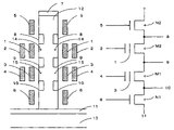
- FIG. 29 is a block diagram of the semiconductor storage device 30 according to the invention.
- the semiconductor storage device 30 includes a plurality of memory cell arrays 31 which each include a plurality of nonvolatile memory devices each including a plurality of memory cells for storing data.
- the memory cell arrays 31 are respectively disposed in blocks B 0 to Bn.
- the blocks B 0 to Bn respectively include local row decoders 32 B 0 to 32 Bn.
- the block B 0 includes the local row decoder 32 B 0 .
- the blocks B 0 to Bn each include a plurality of bit lines 51 S 0 to 51 S 0 i , 51 S 1 to 51 S 1 i , . . . , 51 Sn to 51 Sni extending therein, and a plurality of local word lines (not shown) extending therein.
- the memory cells are respectively disposed at intersections of the local word lines and the bit lines.
- the bit lines for the respective memory cell arrays 31 are connected to a column decoder 36 via a column gate circuit 37 .
- the local word lines of each of the blocks B 0 to Bn are connected to the corresponding local row decoder 32 B 0 to 32 Bn associated with the block B 0 to Bn.
- the memory cell arrays 31 include global word lines 39 S 0 to 39 Sn connected to a global row decoder 35 .
- the global word lines 39 S 0 to 39 Sn are connected to each of the local row decoders 32 B 0 to 32 Bn and extend through the respective blocks B 0 to Bn.
- the global word lines 39 S 0 to 39 Sn are not physically connected to the local word lines of the respective blocks B 0 to Bn, but are adapted to be electrically connected to the local word lines of the respective blocks B 0 to Bn via the local row decoders 32 B 0 to 32 Bn associated with the blocks B 0 to Bn.
- FIG. 30 illustrates each of the memory cell arrays in the blocks B 0 to Bn to be described later.
- the global row decoder 35 is a row decoder for the memory cell arrays 31 , and is adapted to select one of the global word lines 39 S 0 to 39 Sn on the basis of a row address applied through an address bus 49 .
- the local row decoders 32 B 0 to 32 Bn each include a plurality of switching transistors (not shown) which respectively connect the local word lines to the corresponding global word lines 39 S 0 to 39 Sn.
- the local row decoders 32 B 0 to 32 Bn are each adapted to receive a block selection signal from a block decoder 34 . For example, the local row decoder 32 B 0 receives a block selection signal S 0 .
- the switching transistors (not shown) of the respective local row decoders 32 B 0 to 32 Bn are all turned on.
- the switching transistors of the respective local row decoders 32 B 0 to 32 Bn are all in an off state.
- the local word lines of each of the blocks B 0 to Bn are isolated from the global word lines 39 S 0 to 39 Sn, and isolated from the local word lines of the other blocks.
- the local row decoders 32 B 0 to 32 Bn are each adapted to receive an erase control signal, i.e., an erase signal.
- the block decoder 34 is adapted to output one of the block selection signals S 0 to Sn to select the corresponding block. Further, the block decoder 34 is connected to the bus 49 for receiving a block address.
- the blocks B 0 to Bn each include first and second local selection lines (not shown) extending therein.
- the first and second local selection lines of the respective blocks B 0 to Bn are connected to the corresponding local row decoders 32 B 0 to 32 Bn.
- the memory cell arrays 31 further include a plurality of first global selection lines 41 S 0 to 41 Sn and a plurality of second global selection lines 42 S 0 to 42 Sn connected to the global row decoder 35 .
- the first global selection lines 41 S 0 to 41 Sn and the second global selection lines 42 S 0 to 42 Sn are connected to each of the local row decoders 32 B 0 to 32 Bn and extend through the respective blocks B 0 to Bn.
- the first global selection lines 41 S 0 to 41 Sn and the second global selection lines 42 S 0 to 42 Sn are not physically connected to the first and second selection lines of the respective blocks B 0 to Bn of the memory cell arrays 31 , but are adapted to be electrically connected to the first and second local selection lines of the respective blocks B 0 to Bn via the local row decoders 32 B 0 to 32 Bn associated with the blocks B 0 to Bn.
- An erase switch 33 includes a plurality of switches (not shown in FIG. 29 ), which are respectively connected to common source lines 38 S 0 to 38 Sn of the blocks B 0 to Bn.
- the switches of the erase switch 33 connect a voltage (ground voltage) Vg or an erase voltage selectively to the corresponding one of the common source lines 38 S 0 to 38 Sn in the blocks B 0 to Bn in the memory processing operations (i.e., reading, writing and erasing operations).
- the switches of the erase switch 33 apply the voltage Vg to all the common source lines 38 S 0 to 38 Sn irrespective of the block selection signals S 0 to Sn.
- the block decoder 34 outputs a block selection signal indicative of a selected block and applies the erase voltage to the selected block through the corresponding one of the switches of the erase switch 33 .
- the other switches of the erase switch apply the voltage Vg to the other blocks.
- FIG. 30 illustrates a block 60 and a local row decoder 61 associated with the block 60 .
- the block 60 is one of the blocks B 0 to Bn in FIG. 29 .
- the local row decoder 61 is one of the local row decoders 32 B 0 to 32 Bn associated with the block 60 .
- FIG. 30 only global word lines 62 and 63 are shown which extend through the block 60 .
- the global word lines 62 , 63 are two of the global word lines 39 S 0 to 39 Sn in FIG. 29 .
- the block 60 includes bit lines 66 to 66 i .
- the block 60 further includes a first local word line 68 associated with the global word line 63 and a second local word line 67 associated with the global word line 62 .
- the first local word line 68 is connected to the first global word line 63 via a switching transistor 75 of the local row decoder 61
- the second local word line 67 is connected to the second global word line 62 via a switching transistor 74 of the local row decoder 61 .
- the block 60 further includes a first local selection line 72 connected to first selection gates 81 to 81 i of first selection transistors 83 to 83 i of the respective nonvolatile memory devices, and a second local selection line 71 connected to second selection gates 80 to 80 i of second selection transistors 82 to 82 i of the respective nonvolatile memory devices.
- the first local selection line 72 is connected to a first global selection line 70 via a switching transistor 77 of the local row decoder 61
- the second local section line 71 is connected to a second global selection line 69 via a switching transistor 76 of the local row decoder 61 .
- the block 60 has a common source line 73 , which is connected one of the switches of the erase switch 33 ( FIG. 29 ).
- the block 60 further includes memory cells 64 to 64 i and 65 to 65 i .
- the memory cells 65 to 65 i respectively have first control gates 79 to 79 i
- the memory cells 64 to 64 i respectively have second control gates 78 to 78 i .
- the nonvolatile memory devices each have a drain connected to the bit line 66 to 66 i , and a source connected to the common source line 73 .
- the column decoder 36 shown in FIG. 29 includes a drain voltage generating section 43 which generates voltages to be applied to the drains of the nonvolatile memory devices, and is adapted to drive the bit lines 51 S 0 to 51 S 0 i , 51 S 1 to 51 S 1 i , . . . , 51 Sn to 51 Sni ( 66 to 66 i in FIG. 30 ) connected to the drains of the nonvolatile memory devices via the column gate circuit 37 .
- the global row decoder 35 includes a first control gate voltage generating section 44 which generates voltages to be applied to the first control gates ( 79 to 79 i in FIG.
- the global row decoder 35 further includes a first selection gate voltage generating section 46 which generates voltages to be applied to the first selection gates ( 81 to 81 i in FIG.
- the erase switch 33 includes a source voltage generating section 48 which generates voltages to be applied to the sources of the memory devices, and is adapted to drive the common source line 73 connected to the sources of the memory devices.
- the semiconductor storage device 30 further includes a state controlling section 50 which controls signals and voltages to be generated in the semiconductor storage device 30 and the timing for application of the signals and the voltages according to control information applied from the outside of the semiconductor storage device 30 .
- FIG. 3 is a sectional view of a nonvolatile memory device provided in association with a single island semiconductor layer.
- FIG. 4 is an equivalent circuit diagram of the nonvolatile memory device, which is equivalent to each of the nonvolatile memory devices constituting the memory cell array shown in FIG. 30 .
- the nonvolatile memory device of FIG. 3 includes two memory cells M 1 , M 2 each having a charge storage layer 1 , 3 and a control gate 2 , 4 provided around the P-type island semiconductor layer 12 electrically isolated from the P-type semiconductor substrate 13 , and two selection transistors N 1 , N 2 .
- An explanation will be given to voltages to be applied to the respective terminals when the electric charges are injected into either of the charge storage layers 1 , 3 of the memory cells M 1 , M 2 in the nonvolatile memory device in the memory cell array for the writing operation.
- first and second local selection lines 72 , 71 , the first and second local word lines 68 , 67 and the bit line 66 i are selected in the memory cell array shown in FIG. 30 . That is, the first and second local selection lines 72 , 71 , the first and second local word lines 68 , 67 and the bit line 66 i are respectively connected to the first and second selection gate voltage generating sections 46 , 47 , the first and second control gate voltage generating sections 44 , 45 and the drain voltage generating section 43 . Thus, a voltage generated by the first control gate voltage generating section 44 is applied to the first control gate 4 of the nonvolatile memory device via the first local word line 68 .
- a voltage generated by the second control gate voltage generating section 45 is applied to the second control gate 2 of the nonvolatile memory device via the second local word line 67 .
- voltages generated by the first and second selection gate voltage generating sections 46 , 47 and the drain voltage generating section 43 are respectively applied to the first and second selection gates 6 , 5 and the drain 7 via the first and second local selection lines 72 , 71 and the bit line 66 i .
- a voltage generated by the source voltage generating section 48 is applied to the source 11 via the common source line 73 .
- Electric charges are injected into the charge storage layer 3 of the memory cell M 1 the nonvolatile memory device shown in FIG. 4 by an FN tunnel current in the following manner for the writing operation.
- a high voltage VH 1 is applied to the first control gate 4
- a voltage VH 2 (VH 1 >VH 2 ) such as to prevent the writing is applied to the second control gate 2 .
- a positive voltage VH 3 is applied to the second selection gate 5
- a negative voltage VN 1 such as to prevent electrical connection to the source 11 is applied to the first selection gate 6 .
- the source 11 is grounded, and a negative voltage VN 1 is applied to the drain 7 .
- a positive voltage is applied to the drain 7 (bit line) of each of the memory devices, or the drain 7 is grounded for prevention of the writing.
- the negative voltage VN 1 is applied to the drain 7 .
- the N-type diffusion layers 8 , 9 , 10 are kept at the negative voltage VN 1 .
- a first floating channel 15 ( FIG. 3 ) formed in a region of the island semiconductor layer 12 opposed to the charge storage layer 3 with the intervention of an insulation film is charged at the negative voltage VN 1 , whereby a potential difference of VH 1 ⁇ VN 1 occurs between the first control gate 4 and the first floating channel 15 .
- a high voltage VH 1 is applied to the second control gate 2 , and a voltage VH 2 (VH 1 >VH 2 ) such as to prevent the writing is applied to the first control gate 4 .
- a positive voltage VH 3 is applied to the second selection gate 5 , and a negative voltage VN 1 such as to prevent electrical connection to the source 11 is applied to the first selection gate 6 .
- the source 11 is grounded, and a negative voltage VN 1 is applied to the drain 7 into which electric charges are injected.
- a positive voltage is applied to the drain 7 (bit line) of each of the memory devices, or the drain 7 is grounded for prevention of the writing.
- the negative voltage VN 1 is applied to the drain 7 .
- the N-type diffusion layers 8 , 9 , 10 are kept at the negative voltage VN 1 .
- a second floating channel 14 ( FIG. 3 ) formed in a region of the island semiconductor layer 12 opposed to the charge storage layer 1 with the intervention of an insulation film is charged at the negative voltage VN 1 , whereby a potential difference of VH 1 ⁇ VN 1 occurs between the second control gate 2 and the second floating channel 14 .
- the threshold voltage of the memory cell M 2 is positively shifted by the injection of the electric charges.
- the application of the negative voltage VN 1 to the first selection gate 6 prevents the electrical connection between the N-type diffusion layer 10 and the source 11 , thereby preventing the flow of an excessive electric current from the source 11 to the drain 7 to which the negative voltage is applied. Since the electric charges are not injected into the charge storage layer 3 of the memory cell M 1 , the threshold voltage of the memory cell M 1 is not changed. In this manner, the voltages are applied to the respective terminals in the writing operation.
- FIG. 1 is a timing chart for the application of the voltages to the respective terminals according to this embodiment.
- FIG. 2 is a flow chart for the process for the writing operation according to this embodiment. With reference to the flow chart of FIG. 2 , an explanation will be given to the process for the writing operation.
- 0V is applied to the first and second control gates 4 , 2 , the first and second selection gates 6 , 5 , the source 11 and the drain 7 (Step S 01 ). Then, ⁇ 10V, 3V and ⁇ 10V are applied to the drain 7 , the second selection gate 5 and the first selection gate 6 , respectively, with the second control gate 2 being kept at 0V (Step S 02 ). Thereafter, 10V is applied to the first control gate 4 (Step S 03 ). At this time, electric charges are injected into the charge storage layer 3 from the first floating channel 15 by the FN tunnel current. For the other memory devices not subjected to the writing operation in the selected block, 0V is applied to the drain 7 (bit line) of each of the memory devices for prevention of the writing.
- Step S 04 After the completion of the writing, 0V is applied to the first control gate 4 (Step S 04 ). Then, 0V is applied to the first and second selection gates 6 , 5 and the drain 7 (Step SO 5 ).
- the voltages applied to the first and second selection gates 6 , 5 and the drain 7 are simultaneously changed. However, these voltages are not necessarily required to be simultaneously changed, but may be changed in a time-staggered manner.
- a preparatory operation is performed by applying a positive voltage VH 5 to the drain 7 , applying a positive voltage VH 4 (VH 4 >VH 5 ) such as to permit passage of the positive voltage VH 5 to the second selection gate 5 , applying a positive voltage VH 4 to the first control gate 4 and the second control gate 2 , and grounding the first selection gate 6 and the source 11 .
- VH 4 positive voltage
- the second selection gate 5 , the first control gate 4 and the second control gate 2 are turned on and the N-type diffusion layers 8 , 9 , 10 are kept at VH 5 , whereby the first and second floating channels 15 , 14 are charged at VH 5 .
- the voltages applied to the first and second control gates 4 , 2 are changed from the positive voltage VH 4 to a negative voltage VN 1 for the release of the electric charges, whereby a potential difference of VN 1 ⁇ VH 5 occurs between the first control gate 4 and the first floating channel 15 and between the second control gate 2 and the second floating channel 14 .
- the electric charges are released from the charge storage layers 3 , 1 to the first and second floating channels 15 , 14 by an FN tunnel current.
- the threshold voltages of the memory cells M 1 , M 2 are negatively shifted by the release of the electric charges. In this manner, a first exemplary process for the erasing operation is performed.
- the first exemplary process for the erasing operation will be described more specifically with reference to a flow chart shown in FIG. 32 .
- the timing chart for the application of the respective voltages is shown in FIG. 31 .
- 0V is first applied to the first and second control gates 4 , 2 , the first and second selection gates 6 , 5 , the source 11 and the drain 7 (Step S 11 ).
- 10V is applied to the drain 7
- 12V is applied to the second selection gate 5 and the first and second control gates 4 , 2 , whereby the first and second floating channels 15 , 14 are charged (Step S 12 ).
- Step S 13 After the completion of the charging, ⁇ 10V is applied to the first and second control gates 4 , 2 (Step S 13 ). After the completion of the erasing, 0V is applied to the first and second control gates 4 , 2 (Step S 14 ). Thereafter, 0V is applied to the second selection gate 5 and the drain 7 (Step S 15 ).
- 0V is applied to the drain 7 or to the first and second control gates 4 , 2 of each of the memory devices not subjected to the erasing operation for prevention of the erasing.
- 0V is applied to the first and second control gates 4 , 2 and then to the second selection gate 5 and the drain 7 .
- the voltages applied to the second selection gate 5 and the drain 7 are simultaneously changed in FIG. 31 . However, these voltages are not necessarily required to be simultaneously changed, but may be changed in a time-staggered manner. Further, the source 11 and the first selection gate 6 are not necessarily required to be grounded, but a positive voltage may be applied thereto.
- a preparatory operation for the release of the electric charges is performed by applying a positive voltage VH 5 to the source 11 , applying a positive voltage VH 4 (VH 4 >VH 5 ) such as to permit passage of the positive voltage VH 5 to the first selection gate 6 , applying a positive voltage VH 4 to the first control gate 4 and the second control gate 2 , and grounding the second selection gate 5 and the drain 7 .
- the second selection gate 5 , the first control gate 4 and the second control gate 2 are turned on and the N-type diffusion layers 8 , 9 , 10 are kept at VH 5 , whereby the first and second floating channels 15 , 14 are charged at VH 5 .
- the voltages applied to the first and second control gates 4 , 2 are changed from the positive voltage VH 4 to a negative voltage VN 1 for the release of the electric charges, whereby a potential difference of VN 1 ⁇ VH 5 occurs between the first control gate 4 and the first floating channel 15 and between the second control gate 2 and the second floating channel 14 .
- the electric charges are released from the charge storage layers 1 , 3 to the first and second floating channels 15 , 14 by the FN tunnel current.
- the threshold voltages of the memory cells M 1 , M 2 are negatively shifted by the release of the electric charges. In this manner, the second exemplary process for the erasing operation is performed.
- the second exemplary process for the erasing operation will be described more specifically with reference to a flow chart shown in FIG. 34 .
- a timing chart for the application of the respective driving voltages is shown in FIG. 33 .
- 0V is first applied to the first and second control gates 4 , 2 , the first and second selection gates 6 , 5 , the source 11 and the drain 7 (Step S 21 ).
- 10V is applied to the source 11
- 12V is applied to the first selection gate 6 and the first and second control gates 4 , 2 , whereby the first and second floating channels 15 , 14 are charged (Step S 22 ).
- Step S 23 After the completion of the charging, ⁇ 10V is applied to the first and second control gates 4 , 2 (Step S 23 ). After the completion of the erasing, 0V is applied to the first and second control gates 4 , 2 (Step S 24 ). Thereafter, 0V is applied to the second selection gate 5 and the drain 7 (Step S 25 ). In this manner, the memory cells M 1 , M 2 are subjected to the erasing operation. In this process, the voltages applied to the first selection gate 6 and the source 11 are simultaneously changed. However, these voltages are not necessarily required to be simultaneously changed, but may be changed in a time-staggered manner. Further, the drain 7 and the second selection gate 5 are not necessarily required to be grounded, but a positive voltage may be applied thereto.
- a voltage is applied from the drain 7 and the common source 11 .
- a preparatory operation for the release of the electric charges is performed by applying a positive voltage VH 5 to the drain 7 and the source 11 , applying a positive voltage VH 4 (VH 4 >VH 5 ) such as to permit passage of the positive voltage VH 5 to the first and second selection gates 6 , 5 , and applying a positive voltage VH 4 to the first control gate 4 and the second control gate 2 .
- the first and second selection gates 6 , 5 , the first control gate 4 and the second control gate 2 are turned on and the N-type diffusion layers 8 , 9 , 10 are kept at VH 5 , whereby the first and second floating channels 15 , 14 are charged at VH 5 .
- the voltages applied to the first and second control gates 4 , 2 are changed from the positive voltage VH 4 to a negative voltage VN 1 for the release of the electric charges, whereby a potential difference of VN 1 ⁇ VH 5 occurs between the first control gate 4 and the first floating channel 15 and between the second control gate 2 and the second floating channel 14 .
- the electric charges are released from the charge storage layers 3 , 1 to the first and second floating channels 15 , 14 by a tunnel current.
- the threshold voltages of the memory cells M 1 , M 2 are negatively shifted by the release of the electric charges. In this manner, the third exemplary process for the erasing operation is performed.
- the third process for the erasing operation will be described more specifically with reference to a flow chart shown in FIG. 36 .
- a timing chart for the application of the respective voltages is shown in FIG. 35 .
- Step S 31 0V is first applied to the first and second control gates 4 , 2 , the first and second selection gates 6 , 5 , the source 11 and the drain 7 .
- 10V is applied to the drain 7 and the source 11
- 12V is applied to the first and second selection gates 6 , 5 and the first and second control gates 4 , 2 , whereby the first and second floating channels 15 , 14 are charged (Step S 32 ).
- ⁇ 10V is applied to the first and second control gates 4 , 2 (Step S 33 ).
- 0V is applied to the first and second control gates 4 , 2 (Step S 34 ). Thereafter, 0V is applied to the first and second selection gates 6 , 5 , the source 11 and the drain 7 (Step S 35 ). In this manner, the memory cells M 1 , M 2 are subjected to the erasing operation. In this process, the voltages applied to the first and second selection gates 6 , 5 , the drain 7 and the source 11 are simultaneously changed. However, these voltages are not necessarily required to be simultaneously changed, but may be changed in a time-staggered manner.
- the third process for the erasing operation provides a higher channel charging capability to permit higher speed erasing than the first and second processes.
- FIG. 5 is a sectional view of the nonvolatile memory device according to this embodiment.
- FIG. 6 is an equivalent circuit diagram of the nonvolatile memory device.
- FIG. 37 is a diagram illustrating a memory cell array including a plurality of such nonvolatile memory devices.
- the nonvolatile memory device includes one or more memory cells (two memory cells M 3 , M 4 in this embodiment) and a single selection transistor N 3 (hereinafter referred to as “first selection transistor” for easy understanding of the correspondence with the first selection transistor provided in the memory device shown in FIG. 3 ) which are provided in association with a P-type column semiconductor layer 12 electrically isolated from a P-type semiconductor substrate 13 .
- the memory cell array shown in FIG. 37 has substantially the same configuration as the memory cell array ( FIG. 30 ) constituted by the nonvolatile memory devices shown in FIG. 4 , except that the second global selection line 69 and the second local selection line 71 are not provided.
- the first local selection line 72 , the first and second local word lines 68 , 67 and the bit line 66 i are selected. That is, the first local selection line 72 , the first and second local word lines 68 , 67 and the bit line 66 i are respectively connected to the first selection gate voltage generating section 46 , the first and second control gate voltage generating sections 44 , 45 and the drain voltage generating section 43 . Thus, a voltage generated by the first control gate voltage generating section 44 is applied to the first control gate 4 of the nonvolatile memory device via the firs local word line 68 .
- a voltage generated by the second control gate voltage generating section 45 is applied to the second control gate 2 of the nonvolatile memory device via the second local word line 67 .
- voltages generated by the first selection gate voltage generating section 46 and the drain voltage generating section 43 are respectively applied to the first selection gate 6 and the drain 7 via the first local selection line 72 and the bit line 66 i .
- a voltage generated by the source voltage generating section 48 is applied to the source 11 via the common source line 73 .
- Electric charges are injected into the charge storage layer 3 of the memory cell M 3 of the nonvolatile memory device shown in FIG. 6 by an FN tunnel current in the following manner for the writing operation.
- a high voltage VH 1 is applied to the first control gate 4
- a voltage VH 2 (VH 1 >VH 2 ) such as to prevent the writing is applied to the second control gate 2 .
- a negative voltage VN 1 such as to prevent electrical connection to the source 11 is applied to the first selection gate 6 of the first selection transistor N 3 .
- the source 11 is grounded, and a negative voltage VN 1 is applied to the drain 7 .
- a positive voltage is applied to the drain 7 (bit line) of each of the memory devices, or the drain 7 is grounded for prevention of the writing.
- the N-type diffusion layers 8 , 9 , 10 are kept at the negative voltage VN 1 .
- the first floating channel 15 ( FIG. 5 ) formed in a region of the island semiconductor layer 12 opposed to the charge storage layer 3 with the intervention of the insulation film is charged at the negative voltage VN 1 , whereby a potential difference of VH 1 ⁇ VN 1 occurs between the first control gate 4 and the first floating channel 15 ( FIG. 5 ).
- electric charges are injected into the charge storage layer 3 from the first floating channel 15 by the FN tunnel current.
- the threshold voltage of the memory cell M 3 is positively shifted by the injection of the charges.
- the application of the negative voltage VN 1 to the first selection gate 6 prevents electrical connection between the N-type diffusion layer 10 and the source 11 , thereby preventing the flow of an excessive electric current from the source 11 to the drain 7 to which the negative voltage is applied. Since the electric charges are not injected into the charge storage layer 1 of the memory cell M 4 , the threshold voltage of the memory cell M 4 is not changed. In this manner, the electric charges are injected into the charge storage layer 3 of each of the lower memory cells M 3 in the selected block by the FN tunnel current for the writing operation.
- a high voltage VH 1 is applied to the second control gate 2 , and a voltage VH 2 (VH 1 >VH 2 ) such as to prevent the writing is applied to the first control gate 4 .
- a negative voltage VN 1 such as to prevent electrical connection to the source 11 is applied to the first selection gate 6 .
- the source 11 is grounded, and a negative voltage VN 1 is applied to the drain 7 .
- the N-type diffusion layers 9 , 10 are kept at the negative voltage VN 1 .
- the second floating channel 14 formed in a region of the island semiconductor layer 12 opposed to the charge storage layer 1 with the intervention of the insulation film is charged at the negative voltage VN 1 , whereby a potential difference of VH 1 ⁇ VN 1 occurs between the second control gate 2 and the second floating channel 14 .
- the electric charges are injected into the charge storage layer 1 from the second floating channel 14 by the tunnel current.
- the threshold voltage of the memory cell M 4 is positively shifted by the injection of the charges.
- the application of the negative voltage VN 1 to the first selection gate 6 prevents the electrical connection between the N-type diffusion layer 10 and the source 11 , thereby preventing the flow of an excessive electric current from the source 11 to the drain 7 to which the negative voltage is applied. Since the electric charges are not injected into the charge storage layer 3 of the memory cell M 3 , the threshold voltage of the memory cell M 3 is not changed. In this manner, the voltages are applied to the respective terminals for the writing operation.
- FIG. 38 is a timing chart for the application of the voltages to the respective terminals according to this embodiment.
- FIG. 39 is a flow chart for the process for the writing operation according to this embodiment. With reference to the flow chart of FIG. 39 , an explanation will be given to the process for the writing operation on the memory cell.
- 0V is applied to the first and second control gates 4 , 2 , the first selection gate 6 , the source 11 and the drain 7 (Step S 41 ). Then, ⁇ 10V is applied to the drain 7 and the first selection gate 6 with the second control gate 2 being kept at 0V (Step S 42 ). Thereafter, 10V is applied to the first control gate 4 (Step S 43 ). For the other memory devices not subjected to the writing operation in the selected block, 0V is applied to the drain 7 (bit line) of each of the memory devices for prevention of the writing.
- Step S 44 After the completion of the writing, 0V is applied to the first control gate 4 (Step S 44 ). Then, 0V is applied to the first selection gate 6 and the drain 7 (Step S 45 ).
- the voltages applied to the first selection gate 6 and the drain 7 are simultaneously changed. However, these voltages are not necessarily required to be simultaneously changed, but may be changed in a time-staggered manner.
- a preparatory operation is performed by applying a positive voltage VH 5 to the drain 7 , applying a positive voltage VH 4 to the first control gate 4 and the second control gate 2 , and grounding the source 11 and the first selection gate 6 .
- the first control gate 4 and the second control gate 2 are turned on and the N-type diffusion layers 9 , 10 are kept at VH 5 , whereby the first and second floating channels 15 , 14 are charged at VH 5 .
- the voltages applied to the first and second control gates 4 , 2 are changed from the positive voltage VH 4 to a negative voltage VN 1 for the release of the electric charges, whereby a potential difference of VN 1 ⁇ VH 5 occurs between the first control gate 4 and the first floating channel 15 and between the second control gate 2 and the second floating channel 14 .
- the electric charges are released from the charge storage layers 3 , 1 to the first and second floating channels 15 , 14 by an FN tunnel current.
- the threshold voltages of the memory cells M 3 , M 4 are negatively shifted by the release of the electric charges. In this manner, the fourth process for the erasing operation is performed.
- FIG. 40 is a timing chart for the application of the voltages to the respective terminals according to this embodiment.
- FIG. 41 is a flow chart for the fourth process.
- 0V is first applied to the first and second control gates 4 , 2 , the first selection gate 6 , the source 11 and the drain 7 (Step S 51 ).
- 10V is applied to the drain 7
- 12V is applied to the first and second control gates 4 , 2 , whereby the first and second floating channels 15 , 14 are charged (Step S 52 ).
- Step S 53 After the completion of the charging, ⁇ 10V is applied to the first and second control gates 4 , 2 (Step S 53 ). After the completion of the erasing, 0V is applied to the first and second control gates 4 , 2 (Step S 54 ). Thereafter, 0V is applied to the drain 7 (Step S 55 ).
- a preparatory operation is performed by applying a positive voltage VH 5 to the drain 7 and the source 11 , applying a positive voltage VH 4 (VH 4 >VH 5 ) such as to permit passage of the positive voltage VH 5 to the first selection gate 6 , and applying a positive voltage VH 4 to the first control gate 4 and the second control gate 2 .
- the first selection gate 6 , the first control gate 4 and the second control gate 2 are turned on and the N-type diffusion layers 9 , 10 are kept at VH 5 , whereby the first and second floating channels 15 , 14 are charged at VH 5 .
- the voltages applied to the first and second control gates 4 , 2 are changed from the positive voltage VH 4 to a negative voltage VN 1 for the release of the electric charges, whereby a potential difference of VN 1 ⁇ VH 5 occurs between the first control gate 4 and the first floating channel 15 and between the second control gate 2 and the second floating channel 14 .
- the electric charges are released from the charge storage layers 3 , 1 to the first and second floating channels 15 , 14 by a tunnel current.
- the threshold voltages of the memory cells M 3 , M 4 are negatively shifted by the release of the electric charges.
- FIG. 42 is a timing chart for the application of the voltages to the respective terminals in the fifth process.
- FIG. 43 is a flow chart for the fifth process.
- 0V is first applied to the first and second control gates 4 , 2 , the first selection gate 6 , the source 11 and the drain 7 (Step S 61 ).
- 10V is applied to the drain 7 and the source 11
- 12V is applied to the first selection gate 6 and the first and second control gates 4 , 2 , whereby the first and second floating channels 15 , 14 are charged (Step S 62 ).
- Step S 63 After the completion of the charging, ⁇ 10V is applied to the first and second control gates 4 , 2 (Step S 63 ). After the completion of the erasing, 0V is applied to the first and second control gates 4 , 2 (Step S 64 ). Thereafter, 0V is applied to the first selection gate 6 , the source 11 and the drain 7 (Step S 65 ). In this manner, the erasing operation is performed on the memory cells M 3 , M 4 . In this process, the voltages applied to the first selection gate 6 , the drain 7 and the source 11 are simultaneously changed. However, these voltages are not necessarily required to be simultaneously changed, but may be changed in a time-staggered manner.
- the semiconductor storage devices described above are applicable to a rewritable nonvolatile memory for image adjustment in a liquid crystal panel of a liquid crystal display device as shown in FIG. 44 .
- the liquid crystal panel 1001 is driven by a liquid crystal driver 1002 .
- the liquid crystal driver 1002 includes a nonvolatile memory section 1003 , an SRAM section 1004 and a liquid crystal driver circuit 1005 provided therein.
- the nonvolatile memory section 1003 comprises any of the inventive nonvolatile memory devices, preferably the semiconductor storage device according to the second embodiment.
- the nonvolatile memory section 1003 is configured so as to be rewritable from the outside.
- the liquid crystal driver circuit 1005 is capable of reading the information out of the SRAM section 1004 as required.
- the provision of the SRAM section 1004 makes it possible to read out the information at a very high speed.
- the liquid crystal driver 1002 is provided outside the liquid crystal panel 1001 as shown in FIG. 44 , but may be provided on the liquid crystal panel 1001 .
- the liquid crystal panel 1001 is adapted to change the tones of pixels thereof by applying a multi-level voltage to each of the pixels.
- a relationship between the applied voltage and the tone varies from panel to panel. Therefore, information for compensation for the panel-to-panel variation is stored after the production of the liquid crystal panel, and a panel-to-panel variation in image quality is eliminated by the compensation based on the information. Therefore, it is preferred to incorporate the rewritable nonvolatile memory for storing the information for the compensation. Further, it is preferred to employ the inventive memory device, particularly the semiconductor storage device according to the second embodiment, as the nonvolatile memory.
- the negative first voltage is applied to the drain for injecting electric charges to the charge storage layer of the nonvolatile memory device, while 0V or the positive third voltage is applied to the source and the negative first voltage is applied to the first selection gate. Therefore, the flow of the excessive electric current to the drain can be prevented without the need for the provision of the triple well structure which requires a complicated production process.
- the injection of the electric charges into the charge storage layer can be achieved without application of a higher voltage to the control gate. Therefore, the gate width and length of the transistor in the decoder or the booster circuit in the chip can be reduced, so that the area of the chip can be reduced.
- nonvolatile memory device driving method further comprises the steps of: applying the positive fifth voltage to the drain, applying the positive sixth voltage higher than the fifth voltage to the second selection gate and the control gate of the memory cell from which the electric charges are to be released, and applying 0V or the positive seventh voltage to the source and the first selection gate for precharging; and applying the negative eighth voltage to the control gate for releasing the electric charges after the prechargeing step, the release of the electric charges from the charge storage layer of the nonvolatile memory device for the erasing operation can be achieved by applying the negative eighth voltage to the control gate and applying the positive fifth voltage to the drain without applying a higher voltage to the control gate.
- the nonvolatile memory device driving method further comprises the steps of: applying the positive fifth voltage to the source, applying the positive sixth voltage higher than the fifth voltage to the first selection gate and the control gate of the memory cell from which the electric charges are to be released, and applying 0V or the positive seventh voltage to the drain and the second selection gate for precharging; and applying the negative eighth voltage to the control gate for releasing the electric charges after the precharging step, the release of the electric charges from the charge storage layer of the nonvolatile memory device for the erasing operation can be achieved by applying the negative eighth voltage to the control gate and applying the positive fifth voltage to the source without applying a higher voltage to the control gate.
- nonvolatile memory device driving method further comprises the steps of: applying the positive fifth voltage to the drain and the source, and applying the positive sixth voltage higher than the positive fifth voltage to the first selection gate, the second selection gate and the control gate of the memory cell from which the electric charges are to be released for precharging; and applying the negative seventh voltage to the control gate for releasing the electric charges after the precharging step, the release of the electric charges from the charge storage layer can be achieved in a shorter period of time by applying the negative eighth voltage to the control gate and applying the positive fifth voltage to the drain and the source without applying a higher voltage to the control gate.
Abstract
Description
Claims (12)
Applications Claiming Priority (2)
| Application Number | Priority Date | Filing Date | Title |
|---|---|---|---|
| JP2003-197409 | 2003-07-15 | ||
| JP2003197409A JP2005038909A (en) | 2003-07-15 | 2003-07-15 | Drive method of nonvolatile memory element, semiconductor storage device, and liquid crystal display unit provided with it |
Publications (2)
| Publication Number | Publication Date |
|---|---|
| US20050012134A1 US20050012134A1 (en) | 2005-01-20 |
| US7009888B2 true US7009888B2 (en) | 2006-03-07 |
Family
ID=34055864
Family Applications (1)
| Application Number | Title | Priority Date | Filing Date |
|---|---|---|---|
| US10/888,693 Active US7009888B2 (en) | 2003-07-15 | 2004-07-08 | Low voltage, island-layer-based nonvolatile semiconductor storage device with floating biased memory cell channel |
Country Status (4)
| Country | Link |
|---|---|
| US (1) | US7009888B2 (en) |
| JP (1) | JP2005038909A (en) |
| KR (1) | KR100554300B1 (en) |
| TW (1) | TWI246110B (en) |
Cited By (18)
| Publication number | Priority date | Publication date | Assignee | Title |
|---|---|---|---|---|
| US20060181926A1 (en) * | 2005-02-15 | 2006-08-17 | Fujitsu Limited | Semiconductor memory device and method for writing to semiconductor memory device |
| US20070252175A1 (en) * | 2006-03-29 | 2007-11-01 | Micron Technology, Inc. | Floating body transistor constructions, semiconductor constructions, and methods of forming semiconductor constructions |
| US20080237602A1 (en) * | 2007-03-27 | 2008-10-02 | Sandisk 3D Llc | Three dimensional nand memory |
| US20080242008A1 (en) * | 2007-03-27 | 2008-10-02 | Sandisk 3D Llc | Method of making three dimensional nand memory |
| US20080242034A1 (en) * | 2007-03-27 | 2008-10-02 | Sandisk 3D Llc | Method of making three dimensional nand memory |
| US20080237698A1 (en) * | 2007-03-27 | 2008-10-02 | Sandisk 3D Llc | Method of making three dimensional nand memory |
| US20080242028A1 (en) * | 2007-03-27 | 2008-10-02 | Sandisk 3D Llc | Method of making three dimensional nand memory |
| US20080277738A1 (en) * | 2007-05-08 | 2008-11-13 | Venkat Ananthan | Memory cells, memory banks, memory arrays, and electronic systems |
| US20100261324A1 (en) * | 2006-11-01 | 2010-10-14 | Gumbo Logic, Inc. | Trap-charge non-volatile switch connector for programmable logic |
| US7848145B2 (en) | 2007-03-27 | 2010-12-07 | Sandisk 3D Llc | Three dimensional NAND memory |
| US20120025292A1 (en) * | 2010-07-29 | 2012-02-02 | Fujio Masuoka | Nonvolatile semiconductor memory transistor and method for manufacturing nonvolatile semiconductor memory |
| US8320191B2 (en) | 2007-08-30 | 2012-11-27 | Infineon Technologies Ag | Memory cell arrangement, method for controlling a memory cell, memory array and electronic device |
| TWI424536B (en) * | 2007-03-27 | 2014-01-21 | Sandisk 3D Llc | Three dimensional nand memory and method of making thereof |
| US20150243668A1 (en) * | 2012-10-19 | 2015-08-27 | Sharp Kabushiki Kaisha | Non-volatile memory device |
| US9508441B1 (en) | 2015-07-07 | 2016-11-29 | Samsung Electronics Co., Ltd. | Memory device and memory system |
| US11251189B2 (en) | 2009-02-09 | 2022-02-15 | Longitude Flash Memory Solutions Ltd. | Gate fringing effect based channel formation for semiconductor device |
| US11581324B2 (en) * | 2011-02-25 | 2023-02-14 | Micron Technology, Inc. | Charge storage apparatus and methods |
| US11700730B2 (en) | 2010-06-28 | 2023-07-11 | Micron Technology, Inc. | Three dimensional memory and methods of forming the same |
Families Citing this family (2)
| Publication number | Priority date | Publication date | Assignee | Title |
|---|---|---|---|---|
| JP5051342B2 (en) * | 2006-07-12 | 2012-10-17 | ユニサンティス エレクトロニクス シンガポール プライベート リミテッド | Nonvolatile semiconductor memory and driving method thereof |
| EP2302635B1 (en) * | 2009-09-18 | 2016-01-13 | STMicroelectronics Srl | Method for biasing an EEPROM non-volatile memory array and corresponding EEPROM non-volatile memory device |
Citations (7)
| Publication number | Priority date | Publication date | Assignee | Title |
|---|---|---|---|---|
| US4451905A (en) * | 1981-12-28 | 1984-05-29 | Hughes Aircraft Company | Electrically erasable programmable read-only memory cell having a single transistor |
| JPH0479369A (en) | 1990-07-23 | 1992-03-12 | Toshiba Corp | Nonvolatile semiconductor memory |
| US5117392A (en) * | 1989-11-02 | 1992-05-26 | Oki Electric Industry Co., Ltd. | Non-volatile semiconductor memory device |
| US5436552A (en) * | 1992-09-22 | 1995-07-25 | Mitsubishi Denki Kabushiki Kaisha | Clamping circuit for clamping a reference voltage at a predetermined level |
| USRE37311E1 (en) * | 1995-04-06 | 2001-08-07 | Hitachi, Ltd. | Parallel type nonvolatile semiconductor memory device and method of using the same |
| JP2002057231A (en) | 2000-08-11 | 2002-02-22 | Fujio Masuoka | Semiconductor memory device and its manufacturing method |
| US6643210B2 (en) * | 2001-02-16 | 2003-11-04 | Sharp Kabushiki Kaisha | Semiconductor integrated circuit device and method of controlling the same |
-
2003
- 2003-07-15 JP JP2003197409A patent/JP2005038909A/en active Pending
-
2004
- 2004-06-18 TW TW093117585A patent/TWI246110B/en not_active IP Right Cessation
- 2004-07-08 US US10/888,693 patent/US7009888B2/en active Active
- 2004-07-15 KR KR1020040055166A patent/KR100554300B1/en active IP Right Grant
Patent Citations (7)
| Publication number | Priority date | Publication date | Assignee | Title |
|---|---|---|---|---|
| US4451905A (en) * | 1981-12-28 | 1984-05-29 | Hughes Aircraft Company | Electrically erasable programmable read-only memory cell having a single transistor |
| US5117392A (en) * | 1989-11-02 | 1992-05-26 | Oki Electric Industry Co., Ltd. | Non-volatile semiconductor memory device |
| JPH0479369A (en) | 1990-07-23 | 1992-03-12 | Toshiba Corp | Nonvolatile semiconductor memory |
| US5436552A (en) * | 1992-09-22 | 1995-07-25 | Mitsubishi Denki Kabushiki Kaisha | Clamping circuit for clamping a reference voltage at a predetermined level |
| USRE37311E1 (en) * | 1995-04-06 | 2001-08-07 | Hitachi, Ltd. | Parallel type nonvolatile semiconductor memory device and method of using the same |
| JP2002057231A (en) | 2000-08-11 | 2002-02-22 | Fujio Masuoka | Semiconductor memory device and its manufacturing method |
| US6643210B2 (en) * | 2001-02-16 | 2003-11-04 | Sharp Kabushiki Kaisha | Semiconductor integrated circuit device and method of controlling the same |
Cited By (38)
| Publication number | Priority date | Publication date | Assignee | Title |
|---|---|---|---|---|
| US7355893B2 (en) * | 2005-02-15 | 2008-04-08 | Fujitsu Limited | Semiconductor memory device and method for writing to semiconductor memory device |
| US20060181926A1 (en) * | 2005-02-15 | 2006-08-17 | Fujitsu Limited | Semiconductor memory device and method for writing to semiconductor memory device |
| US8946815B2 (en) | 2006-03-29 | 2015-02-03 | Micron Technology, Inc. | Floating body transistor constructions, semiconductor constructions, and methods of forming semiconductor constructions |
| US8501581B2 (en) | 2006-03-29 | 2013-08-06 | Micron Technology, Inc. | Methods of forming semiconductor constructions |
| US20070252175A1 (en) * | 2006-03-29 | 2007-11-01 | Micron Technology, Inc. | Floating body transistor constructions, semiconductor constructions, and methods of forming semiconductor constructions |
| US20100261324A1 (en) * | 2006-11-01 | 2010-10-14 | Gumbo Logic, Inc. | Trap-charge non-volatile switch connector for programmable logic |
| US8139410B2 (en) | 2006-11-01 | 2012-03-20 | Halo Lsi, Inc. | Trap-charge non-volatile switch connector for programmable logic |
| US8089809B2 (en) | 2006-11-01 | 2012-01-03 | Halo Lsi, Inc. | Trap-charge non-volatile switch connector for programmable logic |
| US8027198B2 (en) | 2006-11-01 | 2011-09-27 | Halo Lsi, Inc. | Trap-charge non-volatile switch connector for programmable logic |
| US8023326B2 (en) | 2006-11-01 | 2011-09-20 | Halo Lsi, Inc. | Trap-charge non-volatile switch connector for programmable logic |
| US20100259986A1 (en) * | 2006-11-01 | 2010-10-14 | Gumbo Logic, Inc. | Trap-charge non-volatile switch connector for programmable logic |
| US20100259981A1 (en) * | 2006-11-01 | 2010-10-14 | Gumbo Logic, Inc. | Trap-charge non-volatile switch connector for programmable logic |
| US20100259985A1 (en) * | 2006-11-01 | 2010-10-14 | Gumbo Logic, Inc. | Trap-charge non-volatile switch connector for programmable logic |
| US7851851B2 (en) * | 2007-03-27 | 2010-12-14 | Sandisk 3D Llc | Three dimensional NAND memory |
| US20080242008A1 (en) * | 2007-03-27 | 2008-10-02 | Sandisk 3D Llc | Method of making three dimensional nand memory |
| US7745265B2 (en) | 2007-03-27 | 2010-06-29 | Sandisk 3D, Llc | Method of making three dimensional NAND memory |
| US7575973B2 (en) | 2007-03-27 | 2009-08-18 | Sandisk 3D Llc | Method of making three dimensional NAND memory |
| US7848145B2 (en) | 2007-03-27 | 2010-12-07 | Sandisk 3D Llc | Three dimensional NAND memory |
| US7514321B2 (en) | 2007-03-27 | 2009-04-07 | Sandisk 3D Llc | Method of making three dimensional NAND memory |
| US20080237602A1 (en) * | 2007-03-27 | 2008-10-02 | Sandisk 3D Llc | Three dimensional nand memory |
| US20080242028A1 (en) * | 2007-03-27 | 2008-10-02 | Sandisk 3D Llc | Method of making three dimensional nand memory |
| US20080237698A1 (en) * | 2007-03-27 | 2008-10-02 | Sandisk 3D Llc | Method of making three dimensional nand memory |
| TWI424536B (en) * | 2007-03-27 | 2014-01-21 | Sandisk 3D Llc | Three dimensional nand memory and method of making thereof |
| US20080242034A1 (en) * | 2007-03-27 | 2008-10-02 | Sandisk 3D Llc | Method of making three dimensional nand memory |
| US7808038B2 (en) | 2007-03-27 | 2010-10-05 | Sandisk 3D Llc | Method of making three dimensional NAND memory |
| US20080277738A1 (en) * | 2007-05-08 | 2008-11-13 | Venkat Ananthan | Memory cells, memory banks, memory arrays, and electronic systems |
| US8320191B2 (en) | 2007-08-30 | 2012-11-27 | Infineon Technologies Ag | Memory cell arrangement, method for controlling a memory cell, memory array and electronic device |
| US9030877B2 (en) | 2007-08-30 | 2015-05-12 | Infineon Technologies Ag | Memory cell arrangement, method for controlling a memory cell, memory array and electronic device |
| US11251189B2 (en) | 2009-02-09 | 2022-02-15 | Longitude Flash Memory Solutions Ltd. | Gate fringing effect based channel formation for semiconductor device |
| US11950412B2 (en) | 2009-02-09 | 2024-04-02 | Longitude Flash Memory Solutions Ltd. | Gate fringing effect based channel formation for semiconductor device |
| US11700730B2 (en) | 2010-06-28 | 2023-07-11 | Micron Technology, Inc. | Three dimensional memory and methods of forming the same |
| US20120025292A1 (en) * | 2010-07-29 | 2012-02-02 | Fujio Masuoka | Nonvolatile semiconductor memory transistor and method for manufacturing nonvolatile semiconductor memory |
| US8349688B2 (en) * | 2010-07-29 | 2013-01-08 | Unisantis Electronics Singapore Pte Ltd. | Nonvolatile semiconductor memory transistor and method for manufacturing nonvolatile semiconductor memory |
| US11581324B2 (en) * | 2011-02-25 | 2023-02-14 | Micron Technology, Inc. | Charge storage apparatus and methods |
| US20150243668A1 (en) * | 2012-10-19 | 2015-08-27 | Sharp Kabushiki Kaisha | Non-volatile memory device |
| US9312264B2 (en) * | 2012-10-19 | 2016-04-12 | Sharp Kabushiki Kaisha | Non-volatile memory device |
| TWI567747B (en) * | 2012-10-19 | 2017-01-21 | Sharp Kk | Nonvolatile memory device |
| US9508441B1 (en) | 2015-07-07 | 2016-11-29 | Samsung Electronics Co., Ltd. | Memory device and memory system |
Also Published As
| Publication number | Publication date |
|---|---|
| TWI246110B (en) | 2005-12-21 |
| TW200503059A (en) | 2005-01-16 |
| KR100554300B1 (en) | 2006-02-24 |
| KR20050008538A (en) | 2005-01-21 |
| JP2005038909A (en) | 2005-02-10 |
| US20050012134A1 (en) | 2005-01-20 |
Similar Documents
| Publication | Publication Date | Title |
|---|---|---|
| US7009888B2 (en) | Low voltage, island-layer-based nonvolatile semiconductor storage device with floating biased memory cell channel | |
| KR101056797B1 (en) | Nonvolatile Semiconductor Memory | |
| US6657893B2 (en) | Nonvolatile semiconductor memory device and method for driving the same | |
| US6295227B1 (en) | Non-volatile semiconductor memory device | |
| US6002152A (en) | EEPROM with split gate source side injection with sidewall spacers | |
| JP4114607B2 (en) | Nonvolatile semiconductor memory device and operation method thereof | |
| US6058044A (en) | Shielded bit line sensing scheme for nonvolatile semiconductor memory | |
| US7057230B2 (en) | Nonvolatile semiconductor memory device employing transistors having different gate withstand voltages for enhanced reading speed | |
| US5745417A (en) | Electrically programmable and erasable nonvolatile semiconductor memory device and operating method therefor | |
| EP0678921B1 (en) | Non-volatile semiconductor memory having programming region for injecting and ejecting carrier into and from floating gate | |
| EP2040292B1 (en) | Nonvolatile semiconductor memory and its drive method | |
| US5535158A (en) | Non-volatile semiconductor memory device and method for erasure and production thereof | |
| US5793678A (en) | Parellel type nonvolatile semiconductor memory device method of using the same | |
| US8284616B2 (en) | Trench memory structure operation | |
| US6570788B1 (en) | Semiconductor device and method of driving and method of producing the same | |
| US20100283099A1 (en) | Non-Volatile Semiconductor Memory Device and Manufacturing Method Thereof | |
| KR100364040B1 (en) | A semiconductor memory device and a method of making thereof | |
| US20050051806A1 (en) | Memory cell unit, nonvolatile semiconductor device, and liquid crystal display device including the nonvolatile semiconductor device | |
| JP2006128707A (en) | Flash eeprom memory | |
| US5398202A (en) | Reprogrammable nonvolatile semiconductor memory formed of MOS transistors and reprogramming method thereof | |
| JP2006013336A (en) | Semiconductor storage device and manufacturing method thereof | |
| JPH065873A (en) | Nonvolatile semiconductor memory | |
| KR20100013936A (en) | Flash memory device, operating method and manufacturing method thereof | |
| JPH05114739A (en) | Semiconductor storage device and manufacture thereof | |
| JPH0770233B2 (en) | Writing and erasing method of nonvolatile semiconductor memory device |
Legal Events
| Date | Code | Title | Description |
|---|---|---|---|
| AS | Assignment |
Owner name: MASUOKA, FUJIO, JAPAN Free format text: ASSIGNMENT OF ASSIGNORS INTEREST;ASSIGNORS:MASUOKA, FUJIO;SAKURABA, HIROSHI;MATSUOKA, FUMIYOSHI;AND OTHERS;REEL/FRAME:015567/0964 Effective date: 20040601 Owner name: SHARP KABUSHIKI KAISHA, JAPAN Free format text: ASSIGNMENT OF ASSIGNORS INTEREST;ASSIGNORS:MASUOKA, FUJIO;SAKURABA, HIROSHI;MATSUOKA, FUMIYOSHI;AND OTHERS;REEL/FRAME:015567/0964 Effective date: 20040601 |
|
| STCF | Information on status: patent grant |
Free format text: PATENTED CASE |
|
| CC | Certificate of correction | ||
| FPAY | Fee payment |
Year of fee payment: 4 |
|
| FPAY | Fee payment |
Year of fee payment: 8 |
|
| FEPP | Fee payment procedure |
Free format text: PAYOR NUMBER ASSIGNED (ORIGINAL EVENT CODE: ASPN); ENTITY STATUS OF PATENT OWNER: LARGE ENTITY |
|
| FEPP | Fee payment procedure |
Free format text: PAYER NUMBER DE-ASSIGNED (ORIGINAL EVENT CODE: RMPN); ENTITY STATUS OF PATENT OWNER: LARGE ENTITY Free format text: PAYOR NUMBER ASSIGNED (ORIGINAL EVENT CODE: ASPN); ENTITY STATUS OF PATENT OWNER: LARGE ENTITY |
|
| FPAY | Fee payment |
Year of fee payment: 12 |