US7012863B2 - Rotation control circuit, semiconductor integrated circuit, optical disk drive and method for controlling the same - Google Patents
Rotation control circuit, semiconductor integrated circuit, optical disk drive and method for controlling the same Download PDFInfo
- Publication number
- US7012863B2 US7012863B2 US10/383,061 US38306103A US7012863B2 US 7012863 B2 US7012863 B2 US 7012863B2 US 38306103 A US38306103 A US 38306103A US 7012863 B2 US7012863 B2 US 7012863B2
- Authority
- US
- United States
- Prior art keywords
- pickup
- signal
- controller
- low
- memory
- Prior art date
- Legal status (The legal status is an assumption and is not a legal conclusion. Google has not performed a legal analysis and makes no representation as to the accuracy of the status listed.)
- Expired - Lifetime, expires
Links
- 230000003287 optical effect Effects 0.000 title claims abstract description 117
- 239000004065 semiconductor Substances 0.000 title claims description 50
- 238000000034 method Methods 0.000 title description 18
- 230000015654 memory Effects 0.000 claims abstract description 154
- 230000003321 amplification Effects 0.000 claims description 10
- 238000003199 nucleic acid amplification method Methods 0.000 claims description 10
- 238000010586 diagram Methods 0.000 description 18
- 230000008569 process Effects 0.000 description 11
- 238000006073 displacement reaction Methods 0.000 description 9
- 230000007423 decrease Effects 0.000 description 7
- 230000004048 modification Effects 0.000 description 7
- 238000012986 modification Methods 0.000 description 7
- VYPSYNLAJGMNEJ-UHFFFAOYSA-N Silicium dioxide Chemical compound O=[Si]=O VYPSYNLAJGMNEJ-UHFFFAOYSA-N 0.000 description 5
- 239000000872 buffer Substances 0.000 description 5
- 238000012937 correction Methods 0.000 description 5
- 239000000203 mixture Substances 0.000 description 5
- 239000003990 capacitor Substances 0.000 description 4
- 229910052681 coesite Inorganic materials 0.000 description 4
- 229910052906 cristobalite Inorganic materials 0.000 description 4
- 230000003247 decreasing effect Effects 0.000 description 4
- 230000000694 effects Effects 0.000 description 4
- 229910052751 metal Inorganic materials 0.000 description 4
- 239000002184 metal Substances 0.000 description 4
- 238000012545 processing Methods 0.000 description 4
- 230000005236 sound signal Effects 0.000 description 4
- 229910052682 stishovite Inorganic materials 0.000 description 4
- 229910052905 tridymite Inorganic materials 0.000 description 4
- 229910021420 polycrystalline silicon Inorganic materials 0.000 description 3
- 229920005591 polysilicon Polymers 0.000 description 3
- 239000011347 resin Substances 0.000 description 3
- 229920005989 resin Polymers 0.000 description 3
- 230000001360 synchronised effect Effects 0.000 description 3
- 229910000838 Al alloy Inorganic materials 0.000 description 2
- 229910018125 Al-Si Inorganic materials 0.000 description 2
- 229910018520 Al—Si Inorganic materials 0.000 description 2
- 229910017758 Cu-Si Inorganic materials 0.000 description 2
- 229910017931 Cu—Si Inorganic materials 0.000 description 2
- 229910052782 aluminium Inorganic materials 0.000 description 2
- XAGFODPZIPBFFR-UHFFFAOYSA-N aluminium Chemical compound [Al] XAGFODPZIPBFFR-UHFFFAOYSA-N 0.000 description 2
- 239000005380 borophosphosilicate glass Substances 0.000 description 2
- 230000006870 function Effects 0.000 description 2
- 239000012535 impurity Substances 0.000 description 2
- 230000007246 mechanism Effects 0.000 description 2
- 238000002161 passivation Methods 0.000 description 2
- 239000005360 phosphosilicate glass Substances 0.000 description 2
- 229910021332 silicide Inorganic materials 0.000 description 2
- 239000010936 titanium Substances 0.000 description 2
- 229910020968 MoSi2 Inorganic materials 0.000 description 1
- ZOKXTWBITQBERF-UHFFFAOYSA-N Molybdenum Chemical compound [Mo] ZOKXTWBITQBERF-UHFFFAOYSA-N 0.000 description 1
- 229910052581 Si3N4 Inorganic materials 0.000 description 1
- 229910008479 TiSi2 Inorganic materials 0.000 description 1
- RTAQQCXQSZGOHL-UHFFFAOYSA-N Titanium Chemical compound [Ti] RTAQQCXQSZGOHL-UHFFFAOYSA-N 0.000 description 1
- -1 WSi2 Chemical compound 0.000 description 1
- 229910008814 WSi2 Inorganic materials 0.000 description 1
- 230000001133 acceleration Effects 0.000 description 1
- 230000008901 benefit Effects 0.000 description 1
- DFJQEGUNXWZVAH-UHFFFAOYSA-N bis($l^{2}-silanylidene)titanium Chemical compound [Si]=[Ti]=[Si] DFJQEGUNXWZVAH-UHFFFAOYSA-N 0.000 description 1
- 230000008859 change Effects 0.000 description 1
- 238000013461 design Methods 0.000 description 1
- 239000000428 dust Substances 0.000 description 1
- 238000005516 engineering process Methods 0.000 description 1
- 230000005669 field effect Effects 0.000 description 1
- 230000005484 gravity Effects 0.000 description 1
- 229910052750 molybdenum Inorganic materials 0.000 description 1
- 239000011733 molybdenum Substances 0.000 description 1
- 150000004767 nitrides Chemical class 0.000 description 1
- 229920001721 polyimide Polymers 0.000 description 1
- 239000003870 refractory metal Substances 0.000 description 1
- 230000008929 regeneration Effects 0.000 description 1
- 238000011069 regeneration method Methods 0.000 description 1
- 230000004044 response Effects 0.000 description 1
- FVBUAEGBCNSCDD-UHFFFAOYSA-N silicide(4-) Chemical compound [Si-4] FVBUAEGBCNSCDD-UHFFFAOYSA-N 0.000 description 1
- 239000000377 silicon dioxide Substances 0.000 description 1
- 238000009987 spinning Methods 0.000 description 1
- 230000003068 static effect Effects 0.000 description 1
- 229910052719 titanium Inorganic materials 0.000 description 1
- 238000012546 transfer Methods 0.000 description 1
- WFKWXMTUELFFGS-UHFFFAOYSA-N tungsten Chemical compound [W] WFKWXMTUELFFGS-UHFFFAOYSA-N 0.000 description 1
- 229910052721 tungsten Inorganic materials 0.000 description 1
- 239000010937 tungsten Substances 0.000 description 1
Images


Classifications
-
- G—PHYSICS
- G11—INFORMATION STORAGE
- G11B—INFORMATION STORAGE BASED ON RELATIVE MOVEMENT BETWEEN RECORD CARRIER AND TRANSDUCER
- G11B19/00—Driving, starting, stopping record carriers not specifically of filamentary or web form, or of supports therefor; Control thereof; Control of operating function ; Driving both disc and head
- G11B19/20—Driving; Starting; Stopping; Control thereof
- G11B19/28—Speed controlling, regulating, or indicating
-
- G—PHYSICS
- G11—INFORMATION STORAGE
- G11B—INFORMATION STORAGE BASED ON RELATIVE MOVEMENT BETWEEN RECORD CARRIER AND TRANSDUCER
- G11B7/00—Recording or reproducing by optical means, e.g. recording using a thermal beam of optical radiation by modifying optical properties or the physical structure, reproducing using an optical beam at lower power by sensing optical properties; Record carriers therefor
- G11B2007/0003—Recording, reproducing or erasing systems characterised by the structure or type of the carrier
- G11B2007/0009—Recording, reproducing or erasing systems characterised by the structure or type of the carrier for carriers having data stored in three dimensions, e.g. volume storage
- G11B2007/0013—Recording, reproducing or erasing systems characterised by the structure or type of the carrier for carriers having data stored in three dimensions, e.g. volume storage for carriers having multiple discrete layers
-
- G—PHYSICS
- G11—INFORMATION STORAGE
- G11B—INFORMATION STORAGE BASED ON RELATIVE MOVEMENT BETWEEN RECORD CARRIER AND TRANSDUCER
- G11B7/00—Recording or reproducing by optical means, e.g. recording using a thermal beam of optical radiation by modifying optical properties or the physical structure, reproducing using an optical beam at lower power by sensing optical properties; Record carriers therefor
- G11B7/08—Disposition or mounting of heads or light sources relatively to record carriers
- G11B7/085—Disposition or mounting of heads or light sources relatively to record carriers with provision for moving the light beam into, or out of, its operative position or across tracks, otherwise than during the transducing operation, e.g. for adjustment or preliminary positioning or track change or selection
- G11B7/08505—Methods for track change, selection or preliminary positioning by moving the head
- G11B7/08511—Methods for track change, selection or preliminary positioning by moving the head with focus pull-in only
-
- G—PHYSICS
- G11—INFORMATION STORAGE
- G11B—INFORMATION STORAGE BASED ON RELATIVE MOVEMENT BETWEEN RECORD CARRIER AND TRANSDUCER
- G11B7/00—Recording or reproducing by optical means, e.g. recording using a thermal beam of optical radiation by modifying optical properties or the physical structure, reproducing using an optical beam at lower power by sensing optical properties; Record carriers therefor
- G11B7/08—Disposition or mounting of heads or light sources relatively to record carriers
- G11B7/085—Disposition or mounting of heads or light sources relatively to record carriers with provision for moving the light beam into, or out of, its operative position or across tracks, otherwise than during the transducing operation, e.g. for adjustment or preliminary positioning or track change or selection
- G11B7/08505—Methods for track change, selection or preliminary positioning by moving the head
- G11B7/08517—Methods for track change, selection or preliminary positioning by moving the head with tracking pull-in only
-
- G—PHYSICS
- G11—INFORMATION STORAGE
- G11B—INFORMATION STORAGE BASED ON RELATIVE MOVEMENT BETWEEN RECORD CARRIER AND TRANSDUCER
- G11B7/00—Recording or reproducing by optical means, e.g. recording using a thermal beam of optical radiation by modifying optical properties or the physical structure, reproducing using an optical beam at lower power by sensing optical properties; Record carriers therefor
- G11B7/08—Disposition or mounting of heads or light sources relatively to record carriers
- G11B7/09—Disposition or mounting of heads or light sources relatively to record carriers with provision for moving the light beam or focus plane for the purpose of maintaining alignment of the light beam relative to the record carrier during transducing operation, e.g. to compensate for surface irregularities of the latter or for track following
- G11B7/095—Disposition or mounting of heads or light sources relatively to record carriers with provision for moving the light beam or focus plane for the purpose of maintaining alignment of the light beam relative to the record carrier during transducing operation, e.g. to compensate for surface irregularities of the latter or for track following specially adapted for discs, e.g. for compensation of eccentricity or wobble
- G11B7/0953—Disposition or mounting of heads or light sources relatively to record carriers with provision for moving the light beam or focus plane for the purpose of maintaining alignment of the light beam relative to the record carrier during transducing operation, e.g. to compensate for surface irregularities of the latter or for track following specially adapted for discs, e.g. for compensation of eccentricity or wobble to compensate for eccentricity of the disc or disc tracks
-
- G—PHYSICS
- G11—INFORMATION STORAGE
- G11B—INFORMATION STORAGE BASED ON RELATIVE MOVEMENT BETWEEN RECORD CARRIER AND TRANSDUCER
- G11B7/00—Recording or reproducing by optical means, e.g. recording using a thermal beam of optical radiation by modifying optical properties or the physical structure, reproducing using an optical beam at lower power by sensing optical properties; Record carriers therefor
- G11B7/08—Disposition or mounting of heads or light sources relatively to record carriers
- G11B7/09—Disposition or mounting of heads or light sources relatively to record carriers with provision for moving the light beam or focus plane for the purpose of maintaining alignment of the light beam relative to the record carrier during transducing operation, e.g. to compensate for surface irregularities of the latter or for track following
- G11B7/095—Disposition or mounting of heads or light sources relatively to record carriers with provision for moving the light beam or focus plane for the purpose of maintaining alignment of the light beam relative to the record carrier during transducing operation, e.g. to compensate for surface irregularities of the latter or for track following specially adapted for discs, e.g. for compensation of eccentricity or wobble
- G11B7/0956—Disposition or mounting of heads or light sources relatively to record carriers with provision for moving the light beam or focus plane for the purpose of maintaining alignment of the light beam relative to the record carrier during transducing operation, e.g. to compensate for surface irregularities of the latter or for track following specially adapted for discs, e.g. for compensation of eccentricity or wobble to compensate for tilt, skew, warp or inclination of the disc, i.e. maintain the optical axis at right angles to the disc
Definitions
- the present invention relates to an optical disk drive, and more particularly, relates to a rotation control circuit, a semiconductor integrated circuit, and a method for controlling the same.
- An optical disk drive for a disk such as digital versatile disk (DVD) having two layers requires a number of precise high-speed servo controls of the optical disk such as a focus servo and a tracking servo, in addition to controlling the rotation.
- a focus servo moves the lens in a pickup in the focus direction (direction of optical axis of the lens) based on a focus error signal.
- the tracking servo control track-jump from one particular track to other tracks can be achieved.
- focus servo control focus-jump from one layer to another layer can be achieved.
- An optical disk is fixed to a disk motor by equipment called a clamper.
- the damper cannot fix the optical disk in an ideal condition, because the optical disk has physical dimensional errors. Therefore, an eccentricity may result that means a horizontal shift occurs when the optical disk rotates, and a disk deflection may result that means related error in a shift from perpendicular plane of rotating shaft occurs. That is to say, a relative speed condition between the pickup and the optical disk changes.
- Constant linear velocity (CLV) and constant angular velocity (CAV) control are known as main rotational speed control systems.
- speed of a beam spot on the optical disk also becomes very high.
- the beam spot shifts over the 68 tracks, when the DVD rotates at 16 ⁇ speed with a track pitch is 0.74 ⁇ m and eccentricity quantity of 50 ⁇ m. Therefore, maximum relative speed between the lens and the track reaches 40 KHz, converted into a tracking error signal frequency.
- the control frequency band of a tracking servo generally reaches 5–7 KHz. Therefore, it is not possible to return to a normal operation when the tracking servo deviates at the maximum speed. A vibration of a pickup mechanism created by the eccentricity of the optical disk also considerably increases.
- the relative speed between the optical disk and the pickup lens becomes high when rotational speed of the optical disk becomes very high.
- the servo system loses the controllable frequency band when seek speed between the optical disk and the pickup lens becomes high.
- an open loop gain of the servo system decreases in proportion to an increase in the rotational frequency of the optical disk.
- residual error showing the servo performance increases.
- RF radio frequency
- Seek performance of the optical disk drive also remarkably decreases, when the success probability of the track jump and the layer jump decreases.
- the seek performance decides the performance for reading the data from the optical disk.
- jump failure during high-speed rotation of the disk causes a time loss. Since DVD has only two layers, when the pickup fails to layer jump in one layer of the DVD, the pickup cannot settle in another layer.
- the control must be designed so that the success probability of track jump and layer jump may be improved by the tracking servo and focus servo, since the servo gain can not be sufficiently ensured and such design is very difficult.
- a first aspect of the present invention inheres in a rotation control circuit encompassing, a pickup controller configured to amplify an error signal detected by a pickup from an optical disk, and to generate both a low-frequency component in the error signal and a pickup control signal so as to control the pickup, a memory controller configured to generate a memory address control signal in synchronization with a frequency generator signal provided by a disk motor, a memory circuit configured to store the low-frequency component by using the memory address control signal at a specified timing, a compensation signal adder configured to add the low-frequency component to the pickup control signal at another specified timing, and a system controller configured to control operational timing of the memory controller and the compensation signal adder.
- a second aspect of the present invention inheres in an optical disk drive encompassing, an optical disk, a disk motor configured to drive the optical disk, a pickup configured to emit a light to the optical disk, and to read a reflected light from the optical disk, a rotation control circuit configured to generate both a low-frequency component in an error signal detected by the pickup and a pickup control signal for control of the pickup, and to store the low-frequency component in synchronization with a rotation of the optical disk, and to add the low-frequency component to the pickup control signal, a signal processor configured to provide a reproducing signal and a recording signal to the pickup, a record controller configured to record the recording signal in the optical disk, and a disk motor controller configured to control the rotation of the disk motor.
- a third aspect of the present invention inheres in a semiconductor integrated circuit encompassing, a semiconductor chip, a tracking servo controller integrated on the semiconductor chip and configured to receive a tracking error signal, a focus servo controller integrated on the semiconductor chip and configured to receive a focus error signal, a memory controller integrated on the semiconductor chip and configured to generate a memory address control signal in synchronization with a frequency generator signal provided by a disk motor, a memory circuit integrated on the semiconductor chip and configured to store a low-frequency component in the tracking error signal and the focus error signal by using the memory address control signal at a specified timing, and a compensation signal adder integrated on the semiconductor chip and configured to add the low-frequency component to output signals of the tracking servo controller and the focus servo controller at another specified timing.
- a fourth aspect of the present invention inheres in a method for controlling rotation encompassing, amplifying an error signal detected by a pickup from an optical disk, and generating both a low-frequency component in the error signal and a pickup control signal so as to control the pickup, judging whether a rotational frequency of a disk motor is steady state, storing the low-frequency component in synchronization with a frequency generator signal generated by the disk motor, judging whether the storing is ended, and adding the low-frequency component to the pickup control signal.
- FIG. 1 is a block diagram of an optical disk drive according to a first embodiment of the present invention
- FIG. 2 is a circuit diagram of a tracking servo controller according to the first embodiment of the present invention
- FIG. 3 shows a frequency characteristic of a tracking servo controller according to the first embodiment of the present invention
- FIG. 4 is a functional block diagram of a system controller according to the first embodiment of the present invention.
- FIG. 5 is a block diagram of composition which integrated a part of the optical disk drive according to the first embodiment of the present invention monolithically on the same semiconductor chip;
- FIG. 6 is a mounting example of the semiconductor integrated circuit according to the first embodiment of the present invention.
- FIG. 7A is a schematic diagram of the pickup body
- FIG. 7B is a time chart showing the tracking operation
- FIG. 8 is a flowchart showing a method for controlling the rotation according to the first embodiment of the present invention.
- FIGS. 9A–9E are time charts showing the operation of the rotation control circuit according to the first embodiment of the present invention.
- FIG. 10 is a block diagram of a rotation control circuit according to the modification of a first embodiment of the present invention.
- FIGS. 11A–11C are time charts showing the operation of a rotation control circuit according to a modification of the first embodiment of the present invention.
- FIG. 12 is a block diagram of an optical disk drive according to a second embodiment of the present invention.
- FIG. 13A shows a frequency characteristic of a tracking servo controller according to the second embodiment of the present invention
- FIG. 13B shows a frequency characteristic of a focus servo controller according to the second embodiment of the present invention
- FIG. 14 is a block diagram of composition which integrated a part of the optical disk drive according to the second embodiment of the present invention monolithically on the same semiconductor chip;
- FIG. 15 is a mounting example of the semiconductor integrated circuit according to the second embodiment of the present invention.
- FIG. 16A is a schematic diagram of a focus lens
- FIG. 16B is a time chart showing the focus operation
- FIG. 17 is a flowchart showing a method for controlling the rotation according to the first embodiment of the present invention.
- FIGS. 18A–18E are time charts showing the operation of the rotation control circuit according to the second embodiment of the present invention.
- FIG. 19 is a block diagram of an optical disk drive according to a third embodiment of the present invention.
- FIG. 20 is a schematic diagram showing a condition of a optical disk having large disk deflection
- FIG. 21 is a functional block diagram of a system controller according to the third embodiment of the present invention.
- FIG. 22 is a mounting example of the semiconductor integrated circuit according to the third embodiment of the present invention.
- FIG. 23 is a flowchart showing a method for controlling the rotation according to the third embodiment of the present invention.
- FIGS. 24A–24E are time charts showing the operation of the rotation control circuit according to the third embodiment of the present invention.
- FIG. 25 is a block diagram of an optical disk drive according to a fourth embodiment of the present invention.
- FIG. 26 is a concrete configuration example of a tracking servo controller according to the fourth embodiment of the present invention.
- FIG. 27 is a block diagram of composition which integrated a part of the optical disk drive according to the third embodiment of the present invention monolithically on the same semiconductor chip;
- FIG. 28 is a mounting example of the semiconductor integrated circuit according to the fourth embodiment of the present invention.
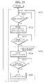
- FIG. 29 is a flowchart showing a method for controlling the rotation according to the fourth embodiment of the present invention.
- FIGS. 30A–30D are time charts showing the operation of the rotation control circuit according to the fourth embodiment of the present invention.
- FIG. 31 is a block diagram of a rotation control circuit according to the modification of the fourth embodiment of the present invention.
- FIG. 32 is a block diagram of a part of a rotation control circuit according to the other embodiment of the present invention.
- FIG. 33 is a block diagram of a part of a rotation control circuit according to the other embodiment of the present invention.
- a compact disk-recordable/rewritable (CD-R/RW) drive is explained as an optical disk drive.
- the data recorded in the optical disk are digital data signals of a video, except for audio signals. It is possible to also realize the DVD drive in the similar configuration.
- a DVD player/recorder is explained as an optical disk drive.
- the data recorded in the optical disk are video, audio signal encoded based on the moving picture experts group 2 (MPEG2) standard.
- MPEG2 moving picture experts group 2
- a optical disk drive includes an optical disk 11 , a pickup 12 , a rotation control circuit 51 a connected to the pickup 12 , a signal processor 77 connected to the rotation control circuit 51 a, a record controller 29 connected to the signal processor 77 , a disk motor controller 23 connected to the rotation control circuit 51 a, a disk motor 13 connected to the disk motor controller 23 .
- the disk motor 13 drives the optical disk 11 .
- the pickup 12 emits a light to optical disk 11
- the pickup 12 reads the reflected light from the optical disk 11 .
- the signal processor 77 processes the signal necessary for reproducing and recording to the pickup 12 .
- the record controller 29 controls the recording based on a record signal generated by signal processor 77 in the optical disk 11 .
- the disk motor controller 23 controls the rotation of the disk motor 13 .
- Rotation control circuit 51 a is connected to an actuator controller 17 , an adder 63 , and an adder 64 .
- the adder 63 and the adder 64 are connected to the lens drive signal generator 22 .
- the rotation control circuit 51 a includes a pickup controller 79 a connected to the pickup 12 , a memory controller 43 connected to the disk motor 13 , a memory circuit 42 connected to the pickup controller 79 a and the memory circuit 42 , a compensation signal adder 41 a connected to the memory circuit 42 and the pickup controller 79 a, and a system controller 25 f connected to the memory controller 43 and the compensation signal adder 41 a.
- the pickup controller 79 a generates both a low-frequency component in the error signal and a pickup control signal necessary for the control of the pickup 12 .
- the memory controller 43 generates a memory address control signal in synchronization with a frequency generator (FG) signal provided by the disk motor 13 .
- FG frequency generator
- the FG signal is angular velocity information provided by the disk motor 13 .
- the memory circuit 42 Using the memory address control signal, the memory circuit 42 , in specific timing, stores the low-frequency component in the error signal.
- the compensation signal adder 41 a in another timing, adds the low-frequency component in the error signal stored in the memory circuit 42 to the pickup control signal.
- a system controller 25 f controls operational timing of memory controller 43 and the compensation signal adder 41 a.
- the pickup controller 79 a includes a radio frequency (RF) amplifier 15 connected to the pickup 12 , a tracking servo controller 16 and a focus servo controller 19 connected to the amplifier 15 .
- the RF amplifier 15 amplifies a tracking error signal TE provided by the pickup 12 .
- the RF amplifier 15 generates a focus error signal FE and a RF signal that is informational signal.
- the memory controller 43 includes a clock generator 30 connected to the disk motor 13 , and a memory address controller 31 having the input side connected to the clock generator 31 and output side connected to the RAM 33 .
- the clock generator 31 multiplies the FG signal provided by the disk motor 13 , and generates a clock of frequency higher than the FG signal.
- Memory address controller 31 is synchronized with the clock and the memory address controller 31 controls the writing and readout address of RAM 33 .
- the clock generator 30 includes a phase comparator connected to the disk motor 13 , a low-pass filter connected to the phase comparator, and a voltage controlled oscillator having an input side connected to the low-pass filter and an output side connected to the phase comparator.
- An output side of the first adder 61 a shown in FIG. 1 is connected to the actuator controller 17 .
- the actuator controller 17 drives an actuator 14 through a motor driver 18 .
- the actuator 14 and motor driver 18 constitute a pickup drive mechanism.
- An output side of the focus servo controller 19 is connected to the adder 64 .
- the adder 64 the output signal of the lens drive signal generator 22 driving the lens in the focus search is added.
- the adder 64 drives the focus actuator in the pickup 12 through actuator driver 21 .
- the RF signal generated by the RF amplifier 15 is transmitted to the signal processor 77 . In reading out, the RF signal is first transmitted to the CD data signal processor 26 a.
- the FG signal from disk motor 13 is transmitted to the disk motor controller 23 .
- the disk motor driver 24 rotational speed of the disk motor 13 is controlled to have a constant angular velocity rotational speed, namely, to control the rotational speed of optical disk 11 .
- a synchronizing signal extracted by the CD data signal processor 26 is transmitted to the disk motor controller 23 .
- rotational speed of the disk motor 13 is controlled to have a constant linear velocity (relative speed between the optical disk 11 and the laser beam) so as to control the rotational speed of optical disk 11 .
- the memory address controller 51 a and the memory circuit 42 in the rotation control circuit 51 a can be monolithically integrated so as to form the semiconductor integrated circuit 95 on the same semiconductor chip 83 a. Furthermore, the signal processor 77 , the lens drive signal generator 22 , record controller 29 , and the disk motor controller 23 are merged in the semiconductor chip 83 a.
- the semiconductor chip 83 a has a bonding pad 91 a configured to supply a signal from the CD data signal processor 26 a.
- the semiconductor chip 83 a also has a bonding pad 91 c configured to supply a signal from the AD converter.
- a bonding pad 91 e is electrically connected to the DA converter 34 .
- a bonding pad 91 f is electrically connected to a bonding pad 91 i.
- a bonding pad 91 g and a bonding pad 91 h are electrically connected to the lens drive signal generator 22 .
- the bonding pad 91 i is electrically connected to the signal processor 77 , to the disk motor controller 23 , to the memory address controller 31 , and to the lens drive signal generator 22 .
- a bonding pad 91 j is electrically connected to the buffer 28 a.
- a bonding pad 91 k is electrically connected to the disk motor controller 23 .
- a bonding pad 91 l is electrically connected to record controller 29 .
- a bonding pad 91 m is electrically connected to the clock generator 30 and the disk motor controller 23 .
- the bonding pads 91 a, 91 c, 91 e – 90 m are connected to, for example, a plurality of high impurity concentration regions (source region/drain region) formed in and at the surfaces of active area assigned at the surface of the semiconductor chip 83 a, where a donor or an acceptor is doped with a concentration of approximately 1 ⁇ 10 18 to 1 ⁇ 10 21 cm ⁇ 3 .
- a plurality of electrode layers made from a metal such as aluminum (Al) or an aluminum alloy (Al—Si, Al—Cu—Si) are formed so as to implement ohmic contacts with this plurality of high impurity concentration regions.
- a passivation film such as an oxide film (SiO 2 ), a phosphosilicate glass (PSG) film, a boro-phosphosilicate glass (BPSG) film, a nitride film (Si 3 N 4 ), or a polyimide film, is deposited.
- a plurality of other bonding pads may be connected, via a plurality of signal lines such as gate wirings, to the polysilicon gate electrodes.
- gate electrodes made of a refractory metal such as tungsten (W), titanium (Ti), or molybdenum (Mo), a silicide (i.e. WSi 2 , TiSi 2 , MoSi 2 ), or a polycide containing any of these silicides can be used.
- the semiconductor integrated circuit 95 shown in FIG. 5 is covered by a mold resin, and a packaged semiconductor integrated circuit 84 a is formed.
- a disk motor terminal 81 k is connected to the bonding pad 91 k.
- a pickup terminal 81 l is connected to the bonding pad 91 l.
- a FG terminal 81 m is connected to the bonding pad 91 m.
- a RF terminal 81 a is connected to the bonding pad 91 a.
- a low-pass filter terminal 81 c is connected to the bonding pad 91 c.
- a memory output terminal 81 e is connected to the bonding pad 91 e.
- An actuator terminal 81 f is connected to the bonding pad 91 f.
- a tracking terminal 81 g is connected to the bonding pad 91 g.
- a focus terminal 81 h is connected to the bonding pad 91 h.
- a system controller terminal 81 i is connected to the bonding pad 91 i.
- a data output terminal 81 j is connected to the bonding pad 91 j.
- the RF terminal 81 a is connected to the RF amplifier 15 .
- the FG terminal 81 m is connected to the disk motor 13 .
- the low-pass filter terminal 81 c is connected to the tracking servo controller 16 .
- the memory output terminal 81 e is connected to the compensation signal adder 41 a.
- the actuator terminal 81 f is connected to the actuator controller 17 .
- the tracking terminal 81 g is connected to the adder 63 .
- the focus terminal 81 h is connected to the adder 64 .
- the system controller terminal 81 i is connected to the system controller 25 f.
- the data output terminal 81 j
- FIGS. 1–4 , FIG. 8 , and FIGS. 9A–9E the operation of the rotation control circuit 51 a according to the first embodiment of the present invention is explained using FIGS. 1–4 , FIG. 8 , and FIGS. 9A–9E .
- the disk motor 13 drives the optical disk 11 .
- the pickup 12 detects the sinusoidal displacement for the effect of the eccentricity of the optical disk 11 in the tracking direction (horizontal direction of the optical disk 11 ). That is to say, the pickup lens repeats the transfer along the outer or inner circumference direction of the optical disk 11 from the mechanical center.
- the RF amplifier 15 amplifies the displacement information, and generates a tracking error signal TE.
- the tracking error signal TE is transmitted to the first high-pass filter 16 a and the first low-pass filter 16 b.
- the first low-pass filter 16 b remove the noise of the tracking error signal TE.
- the first low-pass filter generates the displacement of optical disk 11 tracking direction, namely, “eccentricity data”.
- the clock generator 30 improves the resolution of the FG signal supplied from the disk motor 13 .
- the motor used in the optical disk 11 is mainly a hall motor.
- the hall motor generates the FG signal by hall sensors in the hall motor. Therefore, the pole numbers per one revolution are 6–18 poles, and the resolution of the FG signal is low.
- the clock generator 30 synchronizing with the FG signal provided by the disk motor 13 , generates a high frequency multiplied clock.
- the control of the disk motor is by CAV
- clock generator 30 is designed so that a clock signal is generated for every one clock by rotating 1°.
- FIG. 9D shows the output signal of the RAM 33 in an analog signal by DA converter 34 .
- FIG. 9D shows the output signal of the DA converter 34 in a rotation compensation step, however the DA converter actually generates a continuous signal.
- step S 104 using the eccentricity data of the one revolution minute of the optical disk 11 stored in the RAM 33 starts the rotation compensation.
- the timing controller 24 a in the system controller 25 f turns on the first switching circuit 61 a, and the rotation compensation starts. By turning on the first switching circuit 61 a, the output signal of the DA converter 34 is added to the pickup control signal provided by the tracking servo controller 16 at the first adder 62 a.
- step S 105 the process advances to step S 106 when the stable state judgment portion 25 b shown in FIG. 4 detected the generation of an extraordinary condition or the stop command detector 25 c detected a stop command of the rotation compensation.
- step S 106 the first switching circuit 61 a is turned off, and the rotation compensation ends.
- “extraordinary condition” means the condition that the damper (not illustrated) fixing the optical disk 11 slips or the conditions that dust etc. are adhered to the surface of the optical disk 11 .
- the processing returns to step S 101 , after the rotation compensation completes at step S 106 .
- the rotation control circuit 51 a With the rotation control circuit 51 a according to the first embodiment, an optical disk having a large eccentricity can be reproduced. Moreover, it is possible to sufficiently obtain the gain of the tracking servo controller 16 . Therefore, good tracking servo characteristics of the pickup 12 is obtained, even if the rotational frequency of the optical disk 11 increases. In addition, the pickup 12 can stably carry out track jump.
- the rotational speed of optical disk 11 may change during the steps of storing/reading, since the memory circuit 42 carries out the storing/reading in synchronization with the FG signal generated by disk motor 13 .
- the semiconductor integrated circuit 84 a By merging a part of the optical disk drive according to the first embodiment of the present invention on a semiconductor integrated circuit 84 a, miniaturization and decreased weight of the entire optical disk drive can be achieved. Therefore, the semiconductor integrated circuit 84 a is effective in an optical disk drive such as a portable DVD player.
- a rotation control circuit 51 b has a first compensation signal adder which includes a first adder 62 a connected to the tracking servo controller 16 , and a first amplifier 65 a connected to the first adder 61 a.
- the output side of memory circuit 42 is connected to the input side of the first amplifier 65 a.
- the first switch circuit 41 a shown in FIG. 1 was explained such that the first switch circuit 41 a can only choose ON and OFF in adding the compensation signal (eccentricity data) to the pickup control signal.
- the compensation signal creates a disturbance when the compensation signal read out from memory circuit 42 is suddenly added to the pickup control signal, and then servo deviation, etc. may be caused.
- a rotation control circuit 51 c includes a pickup control circuit 79 b having the RF amplifier 15 connected to the pickup 12 , the tracking servo controller 16 , and a focus servo controller 190 having an input side connected to the RF amplifier 15 and an output side connected to the memory circuit 42 .
- the focus servo controller 120 shown in FIG. 12 includes a second low-pass filter 190 b connected to the RF amplifier 15 , a second high-pass filter 190 a connected to the RF amplifier 15 , and an adder 190 c having one terminal connected to the second low-pass filter 190 b, another terminal connected to the second high-pass filter 190 a.
- the second compensation signal adder 41 b includes a second adder 62 b connected to the focus servo controller 190 , a second switch circuit 61 b connected between the second adder 62 b and the memory circuit 42 .
- a signal processor 78 can reproduce and record the DVD.
- the configuration of the focus servo controller 190 is similar to the configuration of the tracking servo controller 16 shown in FIG. 2 . However, frequency characteristics are different between the focus servo controller 190 and the tracking servo controller 16 , as shown in FIG. 13A and FIG. 13B . The difference originates from characteristics of pickup 12 . Concretely, compared with the first low-pass filter 16 b, as shown in FIG. 13A and FIG. 13B , the second low-pass filter 190 b sets the cut-off frequency low, and sets the gain high. In addition, compared with the first high-pass filter 16 a, the second high-pass filter 190 a sets the cut-off frequency low.
- the RAM 33 of memory circuit 42 stores both the output signal of the first low-pass filter 16 b and the output signal of the second low-pass filter 190 b.
- signal processor 78 of a semiconductor integrated circuit 96 which is merged in a single chip—according to the second embodiment of the present invention has a configuration reproducing and recording a DVD, as shown in FIG. 14 .
- a bonding pad 92 b and a bonding pad 92 c are connected with the AD converter 32 of the memory circuit 42 .
- a bonding pad 92 d and a bonding pad 92 e are connected with the DA converter 34 of the memory circuit 42 .
- a bonding pad 92 j is connected with the MPEG encoder/decoder 28 b of the signal processor 78 .
- a focus low-pass filter terminal is connected with the bonding pad 92 b.
- a second memory output terminal is connected with the bonding pad 92 d.
- a video output terminal is connected with the bonding pad 92 j.
- the semiconductor integrated circuit 96 of the chip shown in FIG. 14 is covered by a mold resin 82 b, as shown in FIG. 15 , and becomes a packaged semiconductor integrated circuit 84 b.
- the focus low-pass filter terminal 85 b is connected to an output side of the second low-pass filter 190 b.
- the second memory output terminal 85 d is connected to the second compensation signal adder 41 b.
- the other elements are similar to the semiconductor integrated circuit 84 a shown in FIG. 6 .
- FIG. 16A and FIG. 16B show the states of layer jumps at (A), (B), (C), and (D) points of a DVD having two layers.
- the lens traces the track, vibrating sinusoidally along the upper and lower directions.
- the lens shifts considerably from the middle position to the upper position, and speed of the lens is sufficiently slow.
- the lens shifts to the lower position, and speed of the lens is very high.
- the lens is the lower position, and speed of the lens is slow.
- the lens shifts to the upper position, and lens is in the middle position.
- the effect of the gravity affects against the layer jump in the horizontal optical disk drive configuration.
- FIG. 4 the operation of the rotation control circuit 51 c according to the second embodiment of the present invention is explained using FIG. 4 , FIGS. 9A–9E , FIG. 17 , and FIGS. 18A–18E .
- description of the operation which is similar to the first embodiment of the present invention is omitted.
- the first low-pass filter 16 b remove the noise of the tracking error signal TE.
- the first low-pass filter 16 b generates the eccentricity data.
- the second low-pass filter 190 b generates the displacement of optical disk 11 focus direction, namely, “disk deflection data”.
- An output signal of the first low-pass filter 16 b and an output signal of the second low-pass filter 190 b are fed into AD converter 32 .
- the AD converter converts the output signal of the first low-pass filter 16 b and the output signal of the second low-pass filter 190 b into analog signal.
- the clock generator 30 generates high frequency clock for improving the resolution of the FG signal supplied from the disk motor 13 .
- the RAM 33 stores the eccentricity data and the disk deflection data of one revolution of optical disk 11 .
- the timing of the storing of eccentricity data and disk deflection data to RAM 33 are mutually independent. Or, the timing of the storing of the eccentricity data and the disk deflection data to RAM 33 are at the same time for the simplification of the processing of the system controller 25 f.
- step S 123 it is judged whether the eccentricity data and the disk deflection data for the one revolution of optical disk 11 is stored in the RAM 33 or not.
- step S 124 it is judged whether the eccentricity data and the disk deflection data for the one revolution of optical disk 11 is stored in the RAM 33 or not.
- step S 104 using the eccentricity data and the disk deflection data for the one revolution of the optical disk 11 stored in RAM 33 , the rotation compensation starts.
- the timing controller 24 a in system controller 25 f turns on the first switching circuit 61 a and the second switching circuit 61 b, the rotation compensation starts.
- the timings of the turning on the first switching circuit 61 a and the second switching circuit 61 b are the same time.
- step S 125 the process advances to step S 126 when the stable state judgment portion 25 b shown in FIG. 4 detected the generation of the extraordinary condition or the stop command detector 25 c detected the stop command of the rotation compensation.
- step S 126 the first switching circuit 61 a and the second switching circuit 61 b are turned off, and the rotation compensation completes.
- the rotation control circuit 51 c according to the second embodiment can reduce residual error of not only tracking servo controller 16 but also focus servo controller 190 , as mentioned above. In addition, it is possible to obtain sufficient the gain of the focus servo controller 190 . Therefore, a good focus servo characteristic of the pickup 12 is obtained, even if the rotational frequency of the optical disk 11 having the disk deflection increases. Therefore, the pickup 12 can stably carry out both track jump and layer jump.
- a compensation signal adder 411 includes a first compensation signal adder 410 a, and a second compensation signal adder 410 b.
- the first compensation signal adder 410 a includes a first adder 62 a connected to an output side of the tracking servo controller 16 , and a first amplifier 65 a connected to the first adder 62 a.
- An input side of the first amplifier 65 a is connected to an output side of the memory circuit 42 .
- the second compensation signal adder 410 b includes a second adder 62 b connected to an output side of the focus servo controller 190 , and a second amplifier 65 b connected to the second adder 62 a. An input side of the second amplifier 65 b is connected to an output side of the memory circuit 42 .
- the system controller 25 g includes a disk deflection calculator 25 d.
- a disk deflection calculator 25 d As shown in FIG. 20 , in the case of reproducing an optical disk having a large disk deflection, a plane of the optical disks 11 considerably tilts for the plane which is perpendicular to the spinning shaft. The proportional relation is formed between a quantity of the disk deflection “a” at B point and a quantity of disk deflection “ba” at the A point, as it is clear from FIG. 20 .
- the disk deflection calculator 25 d calculates the quantity of the disk deflection in every seek, and control an amplification factor Kf of the second amplifier 65 b by the quantity of calculated disk deflection.
- an eccentricity quantity of the inner circumference of the optical disk is equal to an eccentricity quantity of the circumference as for an eccentricity.
- the semiconductor integrated circuit 96 according to the second embodiment of the present invention shown in FIG. 14 is available in a packaged semiconductor integrated circuit 84 c according to the third embodiment of the present invention shown in FIG. 19 .
- a first memory output terminal 86 e shown in FIG. 22 is connected to the first amplifier 65 a.
- a second memory output terminal 86 d is connected to the second amplifier 65 b.
- the other elements are similar to the packaged semiconductor integrated circuit 84 b according to the second embodiment of the present invention shown in FIG. 15 .
- FIGS. 19 – FIG. 21 , FIG. 23 , and FIGS. 24A–24E the operation of the rotation control circuit 51 d according to the third embodiment of the present invention is explained using FIGS. 19 – FIG. 21 , FIG. 23 , and FIGS. 24A–24E .
- description of the operation which is similar to the first and second embodiment of the present invention is omitted.
- the disk deflection data is stored in step S 211 shown in FIG. 23 .
- the memory circuit provides the disk deflection data.
- the disk deflection calculator 25 b shown in FIG. 21 calculates a quantity of the disk deflection. For example, as shown in FIG. 20 , tracking direction of optical disk 11 as an x-axis, pickup 12 moves from an “A” point to a “B” point, and pickup 12 moves to the “A” point again. The disk deflection quantity decreases from the “A” point to the “B” point, and the disk deflection quantity increases from the “B” point to the “A” point. Therefore, the disk deflection calculator 25 d calculates a disk deflection coefficient shown in FIG. 24B .
- the system controller 25 g detects positions where the pickup is located in the point on the x-axis of the optical disk 11 shown in FIG. 20 .
- the disk deflection coefficient is set at the second amplifier 65 b shown in FIG. 19 . As shown in FIG. 24C , an output signal of memory shown in FIG. 24A is multiplied by disk deflection coefficient “b”.
- step S 205 the rotation compensation is started.
- the rotation compensation is started, as shown in FIG. 24C , the amplification factor of the second amplifier 65 b is gradually increased.
- an amplified memory output is generated by the second amplifier 65 b.
- the amplified memory output is transmitted to the second adder 62 b.
- step S 207 the process advances to step S 207 when the stable state judgment portion 25 b in the system controller 25 g detected the generation of an extraordinary condition or the stop command detector 25 c detected a stop command of the rotation compensation.
- step S 207 the amplification factor of the second amplifier becomes zero, and the rotation compensation completes.
- the rotation control circuit 51 d With the rotation control circuit 51 d according to the third embodiment, it is possible that the more accurate disk deflection data is added to an output signal of the focuses servo controller 190 . Therefore, an optical disk having a large disk deflection can be reproduced. In addition, the pickup 12 can stably carry out track jump and layer jump.
- a rotation control circuit 51 e includes a first AD converter 35 connected between the RF amplifier 15 and the tracking servo controller 16 , and second AD converter 36 connected between the RF amplifier 15 and the focus servo controller 191 .
- the memory circuit 420 doesn't include the AD converter 32 and the DA converter 34 shown in FIG. 1 .
- a first high-pass filter 161 a and a first low-pass filter 161 b are composed of digital filters. An output side of the first high-pass filter 161 a and an output side of the first low-pass filter 161 b are connected to an adder 161 c.
- the elements of focus servo controller 191 are similar to the tracking servo controller 161 .
- the tracking servo controller 161 has a frequency characteristic shown in FIG. 3 .
- the focus servo controller 191 has a frequency characteristic shown in FIG. 13B .
- An output side of the first low-pass filter 161 b and an output side of the second low-pass filter 191 b are connected to the memory circuit 420 .
- an input side of a motor driver 18 , an input side of an actuator driver 20 , and an input side of an actuator driver 21 are connected to a DA converter 37 , 38 , and 39 respectively.
- An output signal of the first adder 62 a is transmitted to the actuator controller 17 d.
- the actuator controller 17 d is a digital circuit.
- An output signal of the actuator controller 17 d is converted into an analog signal in the DA converter 37 .
- An output signal of the adder 64 is converted into an analog signal in the DA converter 39 .
- the first AD converter 35 , the second AD converter 36 , the pickup controller 79 c, the compensation signal adder 412 , the memory circuit 420 , the memory controller 43 , the actuator controller 17 d, the lens drive signal generator 22 , the disk motor controller 23 , the record controller 29 , the DA converter 37 , 38 , 39 , the signal processor 78 shown in FIG. 25 can be monolithically integrated so as to form the semiconductor integrated circuit 97 on the same semiconductor chip 83 d.
- a bonding pad 93 a, a bonding pad 93 b, and a bonding pad 93 a are connected to the DA converter 37 , the DA converter 38 , and the DA converter 39 respectively.
- a bonding pad 93 d is connected to the signal processor 78 , the actuator controller 17 d, the disk motor controller 23 , the memory address controller 31 , and the lens drive signal generator 22 .
- a bonding pad 93 f is connected to the disk motor controller 23 .
- a bonding pad 93 g is connected to the record controller 29 .
- a bonding pad 93 h is connected to the clock generator 30 and the disk motor controller 23 .
- a bonding pad 93 k is connected to the DVD data signal processor 26 b.
- a bonding pad 93 i is connected to the second AD converter 36 .
- a bonding pad 93 j is connected to the first AD converter 35 .
- the semiconductor integrated circuit 97 shown in FIG. 27 is covered by a mold resin 82 d, and a packaged semiconductor integrated circuit 84 d is formed.
- a motor driver terminal 87 a is connected to the bonding pad 91 a.
- Actuator driver terminals 87 b, 87 c are connected to the bonding pads 93 b, 93 c respectively.
- a system controller terminal 87 d is connected to the bonding pad 93 d.
- a data output terminal 87 e is connected to the bonding pad 93 e.
- a motor driver terminal 87 f is connected to the bonding pad 93 f.
- a pickup terminal 87 g is connected to the bonding pad 93 g.
- a FG terminal 87 h is connected to the bonding pad 93 h.
- a RF terminal 87 k is connected to the bonding pad 93 k.
- a FE terminal 87 i is connected to the bonding pad 93 i.
- a TE terminal 87 j is connected to the bonding pad 93 j.
- FIG. 4 the operation of the rotation control circuit 51 e according to the fourth embodiment of the present invention is explained using FIG. 4 , FIG. 25 , FIG. 26 , FIG. 29 , and FIGS. 30A–30D .
- description of the operation similar to the first embodiment of the present invention is omitted.
- the pickup 12 detects the sinusoidal displacement for the effect of the eccentricity and the disk deflection of the optical disk 11 in the tracking direction and the focus direction.
- the tracking error signal TE is transmitted to the first AD converter 35 , and the tracking error signal TE is converted into an analog signal.
- the focus error signal FE is transmitted to the second AD converter 36 , and the focus error signal FE is converted into an analog signal.
- the first low-pass filter 161 b generates the eccentricity data.
- step S 221 shown in FIG. 29 the stable state judgment portion 25 b shown in FIG. 4 judges whether the rotational frequency of the disk motor 13 is steady state or not.
- step S 222 When the rotational frequency is judged as the steady state by the steady states judgment portion 25 b at step S 221 , the control advances to step S 222 .
- step S 102 timing controller 25 a shown in FIG. 4 instructs the memory address controller 31 to store the eccentricity data and the disk deflection data corresponding to one revolution of the optical disk 11 .
- step S 223 when the eccentricity data and the disk deflection data for the one revolution of the optical disk 11 were stored in RAM 420 , the process advances to step S 224 .
- step S 224 the rotation compensation starts using the eccentricity data and the disk deflection data of the one revolution of the optical disk 11 stored in the RAM 420 .
- step S 225 the process advances to step S 226 when the stable state judgment portion 25 b shown in FIG. 4 detected the generation of an extraordinary condition or the stop command detector 25 c detected a stop command of the rotation compensation.
- step S 226 the first switching circuit 61 a and the second switching circuit are turned off, and the rotation compensation completes.
- the most part of the optical disk drive shown in FIG. 25 can be composed of the digital circuit. Therefore, the pickup 12 can stably carry out both track jump and layer jump operations, even if the rotational frequency of the optical disk 11 having the eccentricity and the disk deflection increases.
- a first compensation signal adder 41 a includes a first adder 62 a connected to the tracking servo controller 16 , and a first coefficient multiplier 66 a having an output side connected to the first adder 62 a, and an input side connected to the memory circuit 420 .
- a second compensation signal adder 41 b includes a second adder 62 b connected to the focus servo controller 191 , and a second coefficient multiplier 66 b having an output side connected to the second adder 62 b, and an input side connected to the memory circuit 420 .
- the first coefficient multiplier 66 a and the second coefficients multiplier 66 b are mainly constituted by a counter. It is possible to make the multiplier coefficient to zero by resetting the counter. By gradually increasing multiplier coefficient Kt, it is possible that the first adder 62 a gradually transmits the eccentricity data provided by the memory circuit 420 . Moreover, by gradually increasing multiplier coefficient Kf, it is possible that the second adder 62 b gradually transmits the disk deflection data provided by the memory circuit 420 . When the compensation completes, the multiplier coefficient is gradually decreased.
- tracking servo controller 16 is composed of the high-pass filter 16 a and the low-pass filter 16 b in the first embodiment, only the focus servo controller 19 may be composed of high-pass filter and low-pass filter.
- the tracking servo controller 16 , 161 and the focus servo controller 19 , 190 , 191 include the high-pass filter and the low-pass filter.
- a composition which includes a first low-pass filter 162 b connected to an input side of the tracking servo controller 16 , and a second low-pass filter 192 b connected to an input side of the focus servo controller 19 can be used.
- An output side of the first low-pass filter 162 b and an output side of the second low-pass filter 192 b are connected to the memory circuit 42 .
- FIG. 32 a composition which includes a first low-pass filter 162 b connected to an input side of the tracking servo controller 16 , and a second low-pass filter 192 b connected to an input side of the focus servo controller 19 can be used.
- An output side of the first low-pass filter 162 b and an output side of the second low-pass filter 192 b are connected to the memory circuit 42 .
- a composition which includes a first low-pass filter 162 b connected to an output side of the tracking servo controller 16 , and a second low-pass filter 192 b connected to an output side of the focus servo controller 19 can be used.
- various configurations can be used, if the low frequency component of the tracking error signal TE and the focus error signal FE can input it in the memory circuit 42 .
- the semiconductor integrated circuit is implemented by known CMOS process.
- analog circuits such as the tracking servo controller 16 , the focus servo controller 19 , the compensation signal adder 41 a, the actuator controller 17 , and the adders 63 , 64 shown in FIG. 1 can be the monolithically integrated.
- the system controller 25 f can include the disk deflection calculator 25 d shown in FIG. 21 .
- the operation of the rotation control circuit 51 f is similar to the operation of the rotation control circuit 51 d. More specifically, the signals shown in FIG. 24 become digital data.
- the semiconductor integrated circuit 84 d according to the fourth embodiment of the present invention can be formed as system large scale integrated circuit (LSI) by integrating the system controller 25 f on the same semiconductor chip 83 d.
- the wirings connecting respective circuit to the system controller 25 f serves as a bus line.
Abstract
A rotation control circuit comprising, a pickup controller configured to amplify an error signal detected by a pickup from an optical disk, and to generate both a low-frequency component in the error signal and a pickup control signal so as to control the pickup, a memory controller configured to generate a memory address control signal in synchronization with a frequency generator signal provided by a disk motor, a memory circuit configured to store the low-frequency component by using the memory address control signal at a specified timing, a compensation signal adder configured to add the low-frequency component to the pickup control signal at another specified timing, and a system controller configured to control operational timing of the memory controller and the compensation signal adder.
Description
This application is based upon and claims the benefit of priority from prior Japanese Patent Application No. P2002-064437, filed on Mar. 8, 2002; the entire contents of which are incorporated by reference herein.
1. Field of the Invention
The present invention relates to an optical disk drive, and more particularly, relates to a rotation control circuit, a semiconductor integrated circuit, and a method for controlling the same.
2. Description of the Related Art
Recently, with acceleration of optical disk drive speeds, the technology of rotating an optical disk at high-speed close to the limit of a disk motor and a pickup has become widely developed. An optical disk drive for a disk such as digital versatile disk (DVD) having two layers requires a number of precise high-speed servo controls of the optical disk such as a focus servo and a tracking servo, in addition to controlling the rotation. For example, a focus servo moves the lens in a pickup in the focus direction (direction of optical axis of the lens) based on a focus error signal. By the tracking servo control, track-jump from one particular track to other tracks can be achieved. By the focus servo control, focus-jump from one layer to another layer can be achieved.
An optical disk is fixed to a disk motor by equipment called a clamper. However, the damper cannot fix the optical disk in an ideal condition, because the optical disk has physical dimensional errors. Therefore, an eccentricity may result that means a horizontal shift occurs when the optical disk rotates, and a disk deflection may result that means related error in a shift from perpendicular plane of rotating shaft occurs. That is to say, a relative speed condition between the pickup and the optical disk changes.
Constant linear velocity (CLV) and constant angular velocity (CAV) control are known as main rotational speed control systems. In the case of CAV control, a rotational speed of a CD-ROM at 48× speed drive will reach 8640 rpm at 3 (Hz/speed)×48×speed=144 Hz at the circumference of the disk. In the case of a DVD at 16× speed drive, the rotational speed reaches 9600 rpm at 10 (Hz/speed)×16×speed=160 Hz at the circumference of the disk. During the high-speed rotation, speed of a beam spot on the optical disk also becomes very high. The beam spot shifts over the 68 tracks, when the DVD rotates at 16× speed with a track pitch is 0.74 μm and eccentricity quantity of 50 μm. Therefore, maximum relative speed between the lens and the track reaches 40 KHz, converted into a tracking error signal frequency. The control frequency band of a tracking servo generally reaches 5–7 KHz. Therefore, it is not possible to return to a normal operation when the tracking servo deviates at the maximum speed. A vibration of a pickup mechanism created by the eccentricity of the optical disk also considerably increases.
The relative speed between the optical disk and the pickup lens becomes high when rotational speed of the optical disk becomes very high. The servo system loses the controllable frequency band when seek speed between the optical disk and the pickup lens becomes high. As a result, an open loop gain of the servo system decreases in proportion to an increase in the rotational frequency of the optical disk. As a result, residual error showing the servo performance increases. When the residual error increases, a tracking characteristic of the pickup for the eccentricity and the disk deflection deteriorate. Therefore, a radio frequency (RF) signal that is the information signal deteriorates, and the pickup cannot read the data. As a result, it is difficult for the pickup to accurately executes a jump operation of track jump and layer jump. Seek performance of the optical disk drive also remarkably decreases, when the success probability of the track jump and the layer jump decreases. The seek performance decides the performance for reading the data from the optical disk. In addition, jump failure during high-speed rotation of the disk causes a time loss. Since DVD has only two layers, when the pickup fails to layer jump in one layer of the DVD, the pickup cannot settle in another layer. The control must be designed so that the success probability of track jump and layer jump may be improved by the tracking servo and focus servo, since the servo gain can not be sufficiently ensured and such design is very difficult.
A first aspect of the present invention inheres in a rotation control circuit encompassing, a pickup controller configured to amplify an error signal detected by a pickup from an optical disk, and to generate both a low-frequency component in the error signal and a pickup control signal so as to control the pickup, a memory controller configured to generate a memory address control signal in synchronization with a frequency generator signal provided by a disk motor, a memory circuit configured to store the low-frequency component by using the memory address control signal at a specified timing, a compensation signal adder configured to add the low-frequency component to the pickup control signal at another specified timing, and a system controller configured to control operational timing of the memory controller and the compensation signal adder.
A second aspect of the present invention inheres in an optical disk drive encompassing, an optical disk, a disk motor configured to drive the optical disk, a pickup configured to emit a light to the optical disk, and to read a reflected light from the optical disk, a rotation control circuit configured to generate both a low-frequency component in an error signal detected by the pickup and a pickup control signal for control of the pickup, and to store the low-frequency component in synchronization with a rotation of the optical disk, and to add the low-frequency component to the pickup control signal, a signal processor configured to provide a reproducing signal and a recording signal to the pickup, a record controller configured to record the recording signal in the optical disk, and a disk motor controller configured to control the rotation of the disk motor.
A third aspect of the present invention inheres in a semiconductor integrated circuit encompassing, a semiconductor chip, a tracking servo controller integrated on the semiconductor chip and configured to receive a tracking error signal, a focus servo controller integrated on the semiconductor chip and configured to receive a focus error signal, a memory controller integrated on the semiconductor chip and configured to generate a memory address control signal in synchronization with a frequency generator signal provided by a disk motor, a memory circuit integrated on the semiconductor chip and configured to store a low-frequency component in the tracking error signal and the focus error signal by using the memory address control signal at a specified timing, and a compensation signal adder integrated on the semiconductor chip and configured to add the low-frequency component to output signals of the tracking servo controller and the focus servo controller at another specified timing.
A fourth aspect of the present invention inheres in a method for controlling rotation encompassing, amplifying an error signal detected by a pickup from an optical disk, and generating both a low-frequency component in the error signal and a pickup control signal so as to control the pickup, judging whether a rotational frequency of a disk motor is steady state, storing the low-frequency component in synchronization with a frequency generator signal generated by the disk motor, judging whether the storing is ended, and adding the low-frequency component to the pickup control signal.
Various embodiments of the present invention will be described with reference to the accompanying drawings. It is to be noted that the same or similar reference numerals are applied to the same or similar parts and elements throughout the drawings, and description of the same or similar parts and elements will be omitted or simplified. In the following descriptions, numerous specific details are set forth such as specific signal values, etc. to provide a thorough understanding of the present invention. However, it will be obvious to those skilled in the art that the present invention may be practiced without such specific details. In other instances, well-known circuits have been shown in block diagram form in order not to obscure the present invention with unnecessary detail. In the following description, a word “connect” defines a state in which first and second elements are electrically connected to each other without regard to whether or not there is a physical connection between the elements.
In a first practical embodiment of the present invention, a compact disk-recordable/rewritable (CD-R/RW) drive is explained as an optical disk drive. However, the data recorded in the optical disk are digital data signals of a video, except for audio signals. It is possible to also realize the DVD drive in the similar configuration. In second through fourth embodiments of the present invention, a DVD player/recorder is explained as an optical disk drive. However, the data recorded in the optical disk are video, audio signal encoded based on the moving picture experts group 2 (MPEG2) standard.
(First Embodiment)
As shown in FIG. 1 , a optical disk drive according to a first embodiment of the present invention includes an optical disk 11, a pickup 12, a rotation control circuit 51 a connected to the pickup 12, a signal processor 77 connected to the rotation control circuit 51 a, a record controller 29 connected to the signal processor 77, a disk motor controller 23 connected to the rotation control circuit 51 a, a disk motor 13 connected to the disk motor controller 23. The disk motor 13 drives the optical disk 11. The pickup 12 emits a light to optical disk 11, and the pickup 12 reads the reflected light from the optical disk 11. The signal processor 77 processes the signal necessary for reproducing and recording to the pickup 12. The record controller 29 controls the recording based on a record signal generated by signal processor 77 in the optical disk 11. The disk motor controller 23 controls the rotation of the disk motor 13. Rotation control circuit 51 a is connected to an actuator controller 17, an adder 63, and an adder 64. The adder 63 and the adder 64 are connected to the lens drive signal generator 22.
As shown in FIG. 1 , the rotation control circuit 51 a includes a pickup controller 79 a connected to the pickup 12, a memory controller 43 connected to the disk motor 13, a memory circuit 42 connected to the pickup controller 79 a and the memory circuit 42, a compensation signal adder 41 a connected to the memory circuit 42 and the pickup controller 79 a, and a system controller 25 f connected to the memory controller 43 and the compensation signal adder 41 a. The pickup controller 79 a generates both a low-frequency component in the error signal and a pickup control signal necessary for the control of the pickup 12. The memory controller 43 generates a memory address control signal in synchronization with a frequency generator (FG) signal provided by the disk motor 13. The FG signal is angular velocity information provided by the disk motor 13. Using the memory address control signal, the memory circuit 42, in specific timing, stores the low-frequency component in the error signal. The compensation signal adder 41 a, in another timing, adds the low-frequency component in the error signal stored in the memory circuit 42 to the pickup control signal. A system controller 25 f controls operational timing of memory controller 43 and the compensation signal adder 41 a.
As shown in FIG. 1 , the pickup controller 79 a includes a radio frequency (RF) amplifier 15 connected to the pickup 12, a tracking servo controller 16 and a focus servo controller 19 connected to the amplifier 15. The RF amplifier 15 amplifies a tracking error signal TE provided by the pickup 12. In addition, the RF amplifier 15 generates a focus error signal FE and a RF signal that is informational signal.
As shown in FIG. 2 , the tracking servo controller 16 includes first high-pass filter 16 a and a first low-pass filter 16 b connected to the RF amplifier 15, and an adder 16 c having an input terminal connected to the first high-pass filter 16 a, and another input terminal connected to the first low-pass filter 16 b. A second operational amplifier OP2 functions as an input buffer. The first high-pass filter 16 a includes a first resistor R1, a second resistor R2 connected in parallel with the first resistor R1, a second operational amplifier OP2 having a positive input terminal connected to a ground, a first capacitor C1 connected between the first resistor R1 and a negative input terminal of the second operational amplifier OP2, a third resistor R3 connected between an output terminal of the second operational amplifier OP2 and a connection point of the second resistor R2 and the first capacitor C1. The first low-pass filter 16 b includes a third operational amplifier OP3 having a positive input terminal connected to the ground, a fourth resistor R4 connected to a negative input terminal of the third operational amplifier OP3, a second capacitor C2 connected between a output terminal of the third operational amplifier OP3 and a connection point of the negative input terminal of the third operational amplifier OP3 and a output terminal of the third operational amplifier OP3, and an eighth resistor R8 connected in parallel with the second capacitor C2. The adder 16 c includes a fifth resistor R5 connected to output side of the first high-pass filter 16 a, a sixth resistor R6 connected to an output side of the first low-pass filter 16 b, a fourth operational amplifier OP4 having a negative input terminal connected to the fifth resistor R5 and the sixth resistor R6, and a positive input terminal connected to the ground, and a seventh resistor R7 connected between a output terminal of the fourth operational amplifier OP4 and the negative input terminal of the operational amplifier OP4.
As shown in FIG. 3 , the first high-pass filter 16 a and the first low-pass filter 16 b have different frequency characteristics respectively. A broken line shown in FIG. 3 is a frequency characteristics of the whole tracking servo controller 16. An output signal of the first low-pass filter 16 b is used to used to compensate the gain. An output signal of the first high-pass filter 16 a is used to push phase of the tracking error signal TE so as to control the phase. As a result, the output signal of the first low-pass filter 16 b is used as a low frequency component of the error signal generated by the pickup control circuit 79 a. In the case of the CAV control, the low frequency component in the error signal corresponds to a rotational frequency of the optical disk 11. Therefore, in the case of the CD circumference speed of 48× for CAV control, a frequency band of the low frequency component of the error signal is a frequency band of about 160 Hz or less. Whereas, in the case of the DVD with a circumference speed of 16× for a CAV control, a frequency band of a low frequency component of the error signal is in the frequency band of about 144 Hz or less.
The focus error signal FE is transmitted to the focus servo controller 19 shown in FIG. 1 . A focus servo equalizer is contained in focus servo controller 19. For example, the focus servo equalizer includes an anti-alias filter supplied with the focus error signal FE, an AD converter supplied with an output signal of the anti-alias filter, a finite impulse response (FIR) filter supplied with an output signal of the AD converter, and a DA converter supplied with an output signal of the FIR filter.
An output side of the first low-pass filter 16 b is also connected to the memory circuit 42. As shown in FIG. 1 , the memory circuit 42 includes a RAM 33, an AD converter 32 connected to an input side of the RAM 33, and a DA converter 34 connected to an output side of the RAM 33. As the RAM 33, various memories such as a dynamic random access memory (DRAM), static random access memory (SRAM) etc. are available. Storage capacity of the RAM 33 is of a capacity that can store the output signal of the low-pass filter 16 b corresponding to the optical disk 11 of one turn. Concretely, RAM 33 has a bit length of about 16 bits.
The compensation signal adder 41 a includes a first adder 62 a connected to the tracking servo controller 16, and a first switch circuit 61 a connected between the first adder 62 a and the memory circuit 42. As the first switch circuit 61 a, a transistor such as a bipolar junction transistor (BJT), field effect transistor (FET) etc. is available. An output signal of the memory circuit 42 is transmitted to the first switch circuit 61 a. The first switch circuit 61 a switches the connection between the memory circuit 42 and the first adder 62 a.
In addition, the memory controller 43 includes a clock generator 30 connected to the disk motor 13, and a memory address controller 31 having the input side connected to the clock generator 31 and output side connected to the RAM 33. The clock generator 31 multiplies the FG signal provided by the disk motor 13, and generates a clock of frequency higher than the FG signal. Memory address controller 31 is synchronized with the clock and the memory address controller 31 controls the writing and readout address of RAM 33. For example, the clock generator 30 includes a phase comparator connected to the disk motor 13, a low-pass filter connected to the phase comparator, and a voltage controlled oscillator having an input side connected to the low-pass filter and an output side connected to the phase comparator.
As shown in FIG. 4 , the system controller 25 f includes a timing controller 25 a configured to control operation timing of the system of the optical disk drive shown in FIG. 1 . In addition, the system controller 25 f includes a stable state judgment portion 25 b configured to judge whether rotation of the disk motor 13 is steady state or not, and a stop command detector 25 c configured to detect the stop command of the rotation compensation. A read only memory (ROM) 45 a and a random access memory (RAM) 45 b are connected to the system controller 25 f. The ROM 45 a functions as a program memory executed at systems controller 25 f. The RAM 45 b functions as a data memory utilized as a work area or stores data utilized under program execution processing at the system controller 25 f.
An output side of the first adder 61 a shown in FIG. 1 is connected to the actuator controller 17. The actuator controller 17 drives an actuator 14 through a motor driver 18. The actuator 14 and motor driver 18 constitute a pickup drive mechanism. An output side of the focus servo controller 19 is connected to the adder 64. In the adder 64, the output signal of the lens drive signal generator 22 driving the lens in the focus search is added. The adder 64 drives the focus actuator in the pickup 12 through actuator driver 21. The RF signal generated by the RF amplifier 15 is transmitted to the signal processor 77. In reading out, the RF signal is first transmitted to the CD data signal processor 26 a. The CD data signal processor 26 a pulls out a data signal, and converts the data signal into a binary value, and a bit clock and synchronizing signal are extracted. Simultaneously, demodulation and error correction using correction RAM 27 are carried out. Next, buffer 28 a buffers the data, and the data is sent to the host computer.
In recording, the record data supplied by the host computer is buffered by the buffer 28 a. The CD data signal processor 26 a adds ID data and parity bits, etc. to the buffered data. Next, error corrective coding and modulation using correction RAM 27 are carried out. The modulated data are synchronized with the bit clock, and then delivered to the record controller 29. The modulated data are synchronized with the bit clock, and transmit to the record controller 29. The record controller 29 generates laser drive pulses that can form the pit pattern in optical disk 11, and the record controller 29 drives the laser of pickup 12.
In the case of the CAV control, the FG signal from disk motor 13 is transmitted to the disk motor controller 23. Through the disk motor driver 24, rotational speed of the disk motor 13 is controlled to have a constant angular velocity rotational speed, namely, to control the rotational speed of optical disk 11. In the case of the CAV control, a synchronizing signal extracted by the CD data signal processor 26 is transmitted to the disk motor controller 23. Through the disk motor driver 24, rotational speed of the disk motor 13 is controlled to have a constant linear velocity (relative speed between the optical disk 11 and the laser beam) so as to control the rotational speed of optical disk 11.
As shown in FIG. 5 , the memory address controller 51 a and the memory circuit 42 in the rotation control circuit 51 a can be monolithically integrated so as to form the semiconductor integrated circuit 95 on the same semiconductor chip 83 a. Furthermore, the signal processor 77, the lens drive signal generator 22, record controller 29, and the disk motor controller 23 are merged in the semiconductor chip 83 a. The semiconductor chip 83 a has a bonding pad 91 a configured to supply a signal from the CD data signal processor 26 a. The semiconductor chip 83 a also has a bonding pad 91 c configured to supply a signal from the AD converter. A bonding pad 91 e is electrically connected to the DA converter 34. A bonding pad 91 f is electrically connected to a bonding pad 91 i. A bonding pad 91 g and a bonding pad 91 h are electrically connected to the lens drive signal generator 22. The bonding pad 91 i is electrically connected to the signal processor 77, to the disk motor controller 23, to the memory address controller 31, and to the lens drive signal generator 22. A bonding pad 91 j is electrically connected to the buffer 28 a. A bonding pad 91 k is electrically connected to the disk motor controller 23. A bonding pad 91 l is electrically connected to record controller 29. A bonding pad 91 m is electrically connected to the clock generator 30 and the disk motor controller 23. The semiconductor integrated circuit 95 shown in FIG. 5 is implemented by known CMOS process. More specifically, the bonding pads 91 a, 91 c, 91 e–90 m are connected to, for example, a plurality of high impurity concentration regions (source region/drain region) formed in and at the surfaces of active area assigned at the surface of the semiconductor chip 83 a, where a donor or an acceptor is doped with a concentration of approximately 1×10¹⁸ to 1×1021 cm−3. A plurality of electrode layers made from a metal such as aluminum (Al) or an aluminum alloy (Al—Si, Al—Cu—Si) are formed so as to implement ohmic contacts with this plurality of high impurity concentration regions. On the top surface of such a plurality of electrode layers, a passivation film such as an oxide film (SiO2), a phosphosilicate glass (PSG) film, a boro-phosphosilicate glass (BPSG) film, a nitride film (Si3N4), or a polyimide film, is deposited.
A plurality of openings (contact holes) are delineated in a portion of the passivation film so as to expose a plurality of electrode layers, implementing the bonding pads 91 a, 91 c, 91 e–90 m. Alternatively, the bonding pads 91 a, 91 c, 91 e–90 m may be formed as other metal patterns connected to a plurality of electrode layers by using metal wiring. In addition, it is possible to form bonding pads 91 a, 91 c, 91 e–90 m on the polysilicon gate electrodes using a metal film such as aluminum (Al) or an aluminum alloy (Al—Si, Al—Cu—Si). Alternatively, a plurality of other bonding pads may be connected, via a plurality of signal lines such as gate wirings, to the polysilicon gate electrodes. Instead of polysilicon, gate electrodes made of a refractory metal such as tungsten (W), titanium (Ti), or molybdenum (Mo), a silicide (i.e. WSi2, TiSi2, MoSi2), or a polycide containing any of these silicides can be used.
As shown in FIG. 6 , the semiconductor integrated circuit 95 shown in FIG. 5 is covered by a mold resin, and a packaged semiconductor integrated circuit 84 a is formed. A disk motor terminal 81 k is connected to the bonding pad 91 k. A pickup terminal 81 l is connected to the bonding pad 91 l. A FG terminal 81 m is connected to the bonding pad 91 m. A RF terminal 81 a is connected to the bonding pad 91 a. A low-pass filter terminal 81 c is connected to the bonding pad 91 c. A memory output terminal 81 e is connected to the bonding pad 91 e. An actuator terminal 81 f is connected to the bonding pad 91 f. A tracking terminal 81 g is connected to the bonding pad 91 g. A focus terminal 81 h is connected to the bonding pad 91 h. A system controller terminal 81 i is connected to the bonding pad 91 i. A data output terminal 81 j is connected to the bonding pad 91 j. Moreover, the RF terminal 81 a is connected to the RF amplifier 15. The FG terminal 81 m is connected to the disk motor 13. The low-pass filter terminal 81 c is connected to the tracking servo controller 16. The memory output terminal 81 e is connected to the compensation signal adder 41 a. The actuator terminal 81 f is connected to the actuator controller 17. The tracking terminal 81 g is connected to the adder 63. The focus terminal 81 h is connected to the adder 64. The system controller terminal 81 i is connected to the system controller 25 f. The data output terminal 81 j is connected to a host computer.
Next, the operation of the rotation control circuit 51 a according to the first embodiment of the present invention is explained using FIGS. 1–4 , FIG. 8 , and FIGS. 9A–9E .
(A) To begin with, the disk motor 13 drives the optical disk 11. For example, as shown in FIG. 9A , the pickup 12 detects the sinusoidal displacement for the effect of the eccentricity of the optical disk 11 in the tracking direction (horizontal direction of the optical disk 11). That is to say, the pickup lens repeats the transfer along the outer or inner circumference direction of the optical disk 11 from the mechanical center. The RF amplifier 15 amplifies the displacement information, and generates a tracking error signal TE. The tracking error signal TE is transmitted to the first high-pass filter 16 a and the first low-pass filter 16 b. The first low-pass filter 16 b remove the noise of the tracking error signal TE. As shown in FIG. 9B , the first low-pass filter generates the displacement of optical disk 11 tracking direction, namely, “eccentricity data”.
(B) The clock generator 30 improves the resolution of the FG signal supplied from the disk motor 13. Recently, the motor used in the optical disk 11 is mainly a hall motor. The hall motor generates the FG signal by hall sensors in the hall motor. Therefore, the pole numbers per one revolution are 6–18 poles, and the resolution of the FG signal is low. The clock generator 30, synchronizing with the FG signal provided by the disk motor 13, generates a high frequency multiplied clock. When the control of the disk motor is by CAV, the angular velocity of the rotation is fixed. In the case of the CAV control, for example, clock generator 30 is designed so that a clock signal is generated for every one clock by rotating 1°. The clock signal generated by the clock generator 30 is transmitted to the memory address controller 31. In step S101 shown in FIG. 8 , the stable state judgment portion 25 b shown in FIG. 4 judges whether the rotational frequency of the disk motor 13 is steady state or not. When the rotational frequency is not steady state, exact information of the eccentricity cannot be provided by the first low-pass filter 16 b.
(C) When the rotational frequency is judged as the steady state by the steady states judgment portion 25 b at step S101, the control advances to step S102. Next, at step S102, timing controller 25 a shown in FIG. 4 instructs memory address controller 31 to store the eccentricity data corresponding to one revolution of the optical disk 11. The memory address controller 31 generates a memory address control signal. As a result, synchronizing with the clock generated by the clock generator 30, the output signal of the low-pass filter 16 b, namely, the eccentricity data of one revolution of the optical disk 11 is stored in the RAM 33. The RAM 33 stores the eccentricity data of every 2–4° of rotation of the optical disk 11 based on the memory address control signal. The memory address controller 31 judges the end of one revolution by counting the clock provided by the clock generator 30. For example, when the clock generator 30 generates 1° of the rotation of the optical disk 11 by the 1 clock, 360 clocks are counted, and the memory stops storing the eccentricity data. For example, when the clock generator 30 generates one clock by 1° of the rotation of the optical disk 11, 360 clocks are counted, and the memory stops storing the eccentricity data. The first switch circuit 61 a is in an OFF state. At step S103, when the eccentricity data of the one revolution minute of the optical disk 11 was stored in RAM 33, the process advances to step S104.
(D) As shown in FIG. 9D , the output signal of the RAM 33 is converted into an analog signal by DA converter 34. FIG. 9D shows the output signal of the DA converter 34 in a rotation compensation step, however the DA converter actually generates a continuous signal. At step S104, using the eccentricity data of the one revolution minute of the optical disk 11 stored in the RAM 33 starts the rotation compensation. The timing controller 24 a in the system controller 25 f turns on the first switching circuit 61 a, and the rotation compensation starts. By turning on the first switching circuit 61 a, the output signal of the DA converter 34 is added to the pickup control signal provided by the tracking servo controller 16 at the first adder 62 a.
(E) Next, at step S105, the process advances to step S106 when the stable state judgment portion 25 b shown in FIG. 4 detected the generation of an extraordinary condition or the stop command detector 25 c detected a stop command of the rotation compensation. In step S106, the first switching circuit 61 a is turned off, and the rotation compensation ends. Here, “extraordinary condition” means the condition that the damper (not illustrated) fixing the optical disk 11 slips or the conditions that dust etc. are adhered to the surface of the optical disk 11. The processing returns to step S101, after the rotation compensation completes at step S106.
With the rotation control circuit 51 a according to the first embodiment, an optical disk having a large eccentricity can be reproduced. Moreover, it is possible to sufficiently obtain the gain of the tracking servo controller 16. Therefore, good tracking servo characteristics of the pickup 12 is obtained, even if the rotational frequency of the optical disk 11 increases. In addition, the pickup 12 can stably carry out track jump. The rotational speed of optical disk 11 may change during the steps of storing/reading, since the memory circuit 42 carries out the storing/reading in synchronization with the FG signal generated by disk motor 13. By merging a part of the optical disk drive according to the first embodiment of the present invention on a semiconductor integrated circuit 84 a, miniaturization and decreased weight of the entire optical disk drive can be achieved. Therefore, the semiconductor integrated circuit 84 a is effective in an optical disk drive such as a portable DVD player.
As shown in FIG. 10 , a rotation control circuit 51 b according to the modification of the first embodiment of the present invention has a first compensation signal adder which includes a first adder 62 a connected to the tracking servo controller 16, and a first amplifier 65 a connected to the first adder 61 a. The output side of memory circuit 42 is connected to the input side of the first amplifier 65 a. The first switch circuit 41 a shown in FIG. 1 was explained such that the first switch circuit 41 a can only choose ON and OFF in adding the compensation signal (eccentricity data) to the pickup control signal. However, the compensation signal creates a disturbance when the compensation signal read out from memory circuit 42 is suddenly added to the pickup control signal, and then servo deviation, etc. may be caused. When the eccentricity data stored in RAM 33 is added to the zero cross point of the pickup control signal the compensation signal does not become the disturbance. However, it is difficult to store data and to start adding in synchronism with the zero cross point. Therefore, as shown in FIG. 11C , when amplification factor K of the first amplifier 65 a is gradually raised, without creates a compensation signal as a disturbance, it is possible to add the compensation signal to the pickup control signal. Amplification factor K of the first amplifier 65 a is variable. Therefore, it is possible that the amplification factor K is zero. The system controller 25 f shown in FIG. 4 controls the amplification factor K. That is to say, when the signal like FIG. 11A was provided from RAM 33 the compensation signal becomes a signal shown in FIG. 11B as a result of gradually amplifying from the amplification factor K=zero. When the compensation stops, the first adder 65 a gradually decreases until amplification factor K=zero. Therefore, it is possible to freely start or stop adding without limiting storage and readout timing of the data to the RAM 33. Therefore, the compensation operation is always turned on during seek operation.
(Second Embodiment)
As shown in FIG. 12 , a rotation control circuit 51 c according to a second embodiment of the present invention includes a pickup control circuit 79 b having the RF amplifier 15 connected to the pickup 12, the tracking servo controller 16, and a focus servo controller 190 having an input side connected to the RF amplifier 15 and an output side connected to the memory circuit 42. The focus servo controller 120 shown in FIG. 12 includes a second low-pass filter 190 b connected to the RF amplifier 15, a second high-pass filter 190 a connected to the RF amplifier 15, and an adder 190 c having one terminal connected to the second low-pass filter 190 b, another terminal connected to the second high-pass filter 190 a. An output side of the tracking servo controller 16 is connected to a second compensation signal adder 41 b. The second compensation signal adder 41 b includes a second adder 62 b connected to the focus servo controller 190, a second switch circuit 61 b connected between the second adder 62 b and the memory circuit 42. A signal processor 78 can reproduce and record the DVD.
The configuration of the focus servo controller 190 is similar to the configuration of the tracking servo controller 16 shown in FIG. 2 . However, frequency characteristics are different between the focus servo controller 190 and the tracking servo controller 16, as shown in FIG. 13A and FIG. 13B . The difference originates from characteristics of pickup 12. Concretely, compared with the first low-pass filter 16 b, as shown in FIG. 13A and FIG. 13B , the second low-pass filter 190 b sets the cut-off frequency low, and sets the gain high. In addition, compared with the first high-pass filter 16 a, the second high-pass filter 190 a sets the cut-off frequency low. The RAM 33 of memory circuit 42 stores both the output signal of the first low-pass filter 16 b and the output signal of the second low-pass filter 190 b.
The data signal after demodulation and error correction is decoded in the regeneration of the DVD data signal processing circuit 26 in decoder division of MPEG encoder/decoder 28 based on the MPEG2 standard. Then, the original video signal and audio signal are reproduced. The video, audio signal transmitted from an outside source, in the case of recording, is condensed and is encoded in encoder division of MPEG decoder/encoder 28 based on the MPEG2 standard. As a result, the encoded data is generated. The encoded data is transmitted to the DVD signal processor. By using correction RAM 27 in the DVD signal processor 26 b, error corrective coding and modulation are conducted. In addition, signal processor 78 of a semiconductor integrated circuit 96—which is merged in a single chip—according to the second embodiment of the present invention has a configuration reproducing and recording a DVD, as shown in FIG. 14 . A bonding pad 92 b and a bonding pad 92 c are connected with the AD converter 32 of the memory circuit 42. A bonding pad 92 d and a bonding pad 92 e are connected with the DA converter 34 of the memory circuit 42. A bonding pad 92 j is connected with the MPEG encoder/decoder 28 b of the signal processor 78. As shown in FIG. 15 , a focus low-pass filter terminal is connected with the bonding pad 92 b. A second memory output terminal is connected with the bonding pad 92 d. A video output terminal is connected with the bonding pad 92 j.
The semiconductor integrated circuit 96 of the chip shown in FIG. 14 is covered by a mold resin 82 b, as shown in FIG. 15 , and becomes a packaged semiconductor integrated circuit 84 b. The focus low-pass filter terminal 85 b is connected to an output side of the second low-pass filter 190 b. The second memory output terminal 85 d is connected to the second compensation signal adder 41 b. The other elements are similar to the semiconductor integrated circuit 84 a shown in FIG. 6 .
Next, the operation of the rotation control circuit 51 c according to the second embodiment of the present invention is explained using FIG. 4 , FIGS. 9A–9E , FIG. 17 , and FIGS. 18A–18E . However, description of the operation which is similar to the first embodiment of the present invention is omitted.
(A) To begin with, as shown in FIG. 9A and FIG. 18A , sinusoidal displacement in the tracking direction and focus direction are generated by effect of the eccentricity and the disk deflection between the pickup 12 and the optical disk 11. The RF amplifier 15 amplifies the displacement information, and generates the tracking error signal TE and the focus error signal FE. Tracking error signal TE and focus error signal FE are fed into tracking servo controller 16 and focus error controller 190 respectively.
(B) Next, the first low-pass filter 16 b remove the noise of the tracking error signal TE. As shown in FIG. 9B , the first low-pass filter 16 b generates the eccentricity data. As shown in FIG. 18B , the second low-pass filter 190 b generates the displacement of optical disk 11 focus direction, namely, “disk deflection data”. An output signal of the first low-pass filter 16 b and an output signal of the second low-pass filter 190 b are fed into AD converter 32. As shown in FIG. 9C and FIG. 18C , the AD converter converts the output signal of the first low-pass filter 16 b and the output signal of the second low-pass filter 190 b into analog signal.
(C) Next, the clock generator 30 generates high frequency clock for improving the resolution of the FG signal supplied from the disk motor 13. When the rotational frequency is judged as the steady state by the steady states judgment portion 25 b at step S121 shown in FIG. 17 , the RAM 33 stores the eccentricity data and the disk deflection data of one revolution of optical disk 11. Here, the timing of the storing of eccentricity data and disk deflection data to RAM 33 are mutually independent. Or, the timing of the storing of the eccentricity data and the disk deflection data to RAM 33 are at the same time for the simplification of the processing of the system controller 25 f. Next, the eccentricity data and the disk deflection data are stored in the RAM 33 in synchronism with the clock signal generated by the clock generator 30. At step S123, it is judged whether the eccentricity data and the disk deflection data for the one revolution of optical disk 11 is stored in the RAM 33 or not. When the eccentricity and disk deflection data are judged to be stored in the RAM 33 the process advances to step S124.
(D) Next, at step S104, using the eccentricity data and the disk deflection data for the one revolution of the optical disk 11 stored in RAM 33, the rotation compensation starts. The timing controller 24 a in system controller 25 f turns on the first switching circuit 61 a and the second switching circuit 61 b, the rotation compensation starts. For example, the timings of the turning on the first switching circuit 61 a and the second switching circuit 61 b are the same time.
(E) Next, at step S125, the process advances to step S126 when the stable state judgment portion 25 b shown in FIG. 4 detected the generation of the extraordinary condition or the stop command detector 25 c detected the stop command of the rotation compensation. In step S126, the first switching circuit 61 a and the second switching circuit 61 b are turned off, and the rotation compensation completes.
The rotation control circuit 51 c according to the second embodiment can reduce residual error of not only tracking servo controller 16 but also focus servo controller 190, as mentioned above. In addition, it is possible to obtain sufficient the gain of the focus servo controller 190. Therefore, a good focus servo characteristic of the pickup 12 is obtained, even if the rotational frequency of the optical disk 11 having the disk deflection increases. Therefore, the pickup 12 can stably carry out both track jump and layer jump.
(Third Embodiment)
As shown in FIG. 19 , the configuration of the focus servo controller 190 is similar to the configuration of the focus servo controller 16 shown in FIG. 10 . A compensation signal adder 411 includes a first compensation signal adder 410 a, and a second compensation signal adder 410 b. The first compensation signal adder 410 a includes a first adder 62 a connected to an output side of the tracking servo controller 16, and a first amplifier 65 a connected to the first adder 62 a. An input side of the first amplifier 65 a is connected to an output side of the memory circuit 42. The second compensation signal adder 410 b includes a second adder 62 b connected to an output side of the focus servo controller 190, and a second amplifier 65 b connected to the second adder 62 a. An input side of the second amplifier 65 b is connected to an output side of the memory circuit 42.
As shown in FIG. 21 , the system controller 25 g includes a disk deflection calculator 25 d. As shown in FIG. 20 , in the case of reproducing an optical disk having a large disk deflection, a plane of the optical disks 11 considerably tilts for the plane which is perpendicular to the spinning shaft. The proportional relation is formed between a quantity of the disk deflection “a” at B point and a quantity of disk deflection “ba” at the A point, as it is clear from FIG. 20 . The disk deflection calculator 25 d calculates the quantity of the disk deflection in every seek, and control an amplification factor Kf of the second amplifier 65 b by the quantity of calculated disk deflection. In addition, an eccentricity quantity of the inner circumference of the optical disk is equal to an eccentricity quantity of the circumference as for an eccentricity.
The semiconductor integrated circuit 96 according to the second embodiment of the present invention shown in FIG. 14 is available in a packaged semiconductor integrated circuit 84 c according to the third embodiment of the present invention shown in FIG. 19 . A first memory output terminal 86 e shown in FIG. 22 is connected to the first amplifier 65 a. A second memory output terminal 86 d is connected to the second amplifier 65 b. The other elements are similar to the packaged semiconductor integrated circuit 84 b according to the second embodiment of the present invention shown in FIG. 15 .
Next, the operation of the rotation control circuit 51 d according to the third embodiment of the present invention is explained using FIGS. 19–FIG. 21 , FIG. 23 , and FIGS. 24A–24E . However, description of the operation which is similar to the first and second embodiment of the present invention is omitted.
(A) To begin with, the disk deflection data is stored in step S211 shown in FIG. 23 . As shown in FIG. 24A , the memory circuit provides the disk deflection data.
(B) Next, the disk deflection calculator 25 b shown in FIG. 21 calculates a quantity of the disk deflection. For example, as shown in FIG. 20 , tracking direction of optical disk 11 as an x-axis, pickup 12 moves from an “A” point to a “B” point, and pickup 12 moves to the “A” point again. The disk deflection quantity decreases from the “A” point to the “B” point, and the disk deflection quantity increases from the “B” point to the “A” point. Therefore, the disk deflection calculator 25 d calculates a disk deflection coefficient shown in FIG. 24B . Here, the system controller 25 g detects positions where the pickup is located in the point on the x-axis of the optical disk 11 shown in FIG. 20 . Next, the disk deflection coefficient is set at the second amplifier 65 b shown in FIG. 19 . As shown in FIG. 24C , an output signal of memory shown in FIG. 24A is multiplied by disk deflection coefficient “b”.
(C) Next, at step S205, the rotation compensation is started. When the rotation compensation is started, as shown in FIG. 24C , the amplification factor of the second amplifier 65 b is gradually increased. As shown in FIG. 24E , an amplified memory output is generated by the second amplifier 65 b. The amplified memory output is transmitted to the second adder 62 b.
(D) Next, the process advances to step S207 when the stable state judgment portion 25 b in the system controller 25 g detected the generation of an extraordinary condition or the stop command detector 25 c detected a stop command of the rotation compensation. In step S207, the amplification factor of the second amplifier becomes zero, and the rotation compensation completes.
With the rotation control circuit 51 d according to the third embodiment, it is possible that the more accurate disk deflection data is added to an output signal of the focuses servo controller 190. Therefore, an optical disk having a large disk deflection can be reproduced. In addition, the pickup 12 can stably carry out track jump and layer jump.
(Fourth Embodiment)
As shown in FIG. 25 , a rotation control circuit 51 e according to the fourth embodiment of the present invention includes a first AD converter 35 connected between the RF amplifier 15 and the tracking servo controller 16, and second AD converter 36 connected between the RF amplifier 15 and the focus servo controller 191. The memory circuit 420 doesn't include the AD converter 32 and the DA converter 34 shown in FIG. 1 . As shown in FIG. 26 , a first high-pass filter 161 a and a first low-pass filter 161 b are composed of digital filters. An output side of the first high-pass filter 161 a and an output side of the first low-pass filter 161 b are connected to an adder 161 c. The elements of focus servo controller 191 are similar to the tracking servo controller 161. The tracking servo controller 161 has a frequency characteristic shown in FIG. 3 . The focus servo controller 191 has a frequency characteristic shown in FIG. 13B . An output side of the first low-pass filter 161 b and an output side of the second low-pass filter 191 b are connected to the memory circuit 420.
In outside of the rotation control circuit 51 e, an input side of a motor driver 18, an input side of an actuator driver 20, and an input side of an actuator driver 21 are connected to a DA converter 37, 38, and 39 respectively. An output signal of the first adder 62 a is transmitted to the actuator controller 17 d. The actuator controller 17 d is a digital circuit. An output signal of the actuator controller 17 d is converted into an analog signal in the DA converter 37. An output signal of the adder 64 is converted into an analog signal in the DA converter 39.
As shown in FIG. 27 , The first AD converter 35, the second AD converter 36, the pickup controller 79 c, the compensation signal adder 412, the memory circuit 420, the memory controller 43, the actuator controller 17 d, the lens drive signal generator 22, the disk motor controller 23, the record controller 29, the DA converter 37,38,39, the signal processor 78 shown in FIG. 25 can be monolithically integrated so as to form the semiconductor integrated circuit 97 on the same semiconductor chip 83 d. As shown in FIG. 27 , A bonding pad 93 a, a bonding pad 93 b, and a bonding pad 93 a are connected to the DA converter 37, the DA converter 38, and the DA converter 39 respectively. A bonding pad 93 d is connected to the signal processor 78, the actuator controller 17 d, the disk motor controller 23, the memory address controller 31, and the lens drive signal generator 22. A bonding pad 93 f is connected to the disk motor controller 23. A bonding pad 93 g is connected to the record controller 29. A bonding pad 93 h is connected to the clock generator 30 and the disk motor controller 23. A bonding pad 93 k is connected to the DVD data signal processor 26 b. A bonding pad 93 i is connected to the second AD converter 36. A bonding pad 93 j is connected to the first AD converter 35.
As shown in FIG. 28 , the semiconductor integrated circuit 97 shown in FIG. 27 is covered by a mold resin 82 d, and a packaged semiconductor integrated circuit 84 d is formed. A motor driver terminal 87 a is connected to the bonding pad 91 a. Actuator driver terminals 87 b, 87 c are connected to the bonding pads 93 b, 93 c respectively. A system controller terminal 87 d is connected to the bonding pad 93 d. A data output terminal 87 e is connected to the bonding pad 93 e. A motor driver terminal 87 f is connected to the bonding pad 93 f. A pickup terminal 87 g is connected to the bonding pad 93 g. A FG terminal 87 h is connected to the bonding pad 93 h. A RF terminal 87 k is connected to the bonding pad 93 k. A FE terminal 87 i is connected to the bonding pad 93 i. A TE terminal 87 j is connected to the bonding pad 93 j.
Next, the operation of the rotation control circuit 51 e according to the fourth embodiment of the present invention is explained using FIG. 4 , FIG. 25 , FIG. 26 , FIG. 29 , and FIGS. 30A–30D . However, description of the operation similar to the first embodiment of the present invention is omitted.
(A) For example, as shown in FIG. 30A , the pickup 12 detects the sinusoidal displacement for the effect of the eccentricity and the disk deflection of the optical disk 11 in the tracking direction and the focus direction. The tracking error signal TE is transmitted to the first AD converter 35, and the tracking error signal TE is converted into an analog signal. The focus error signal FE is transmitted to the second AD converter 36, and the focus error signal FE is converted into an analog signal. As shown in FIG. 30B , the first low-pass filter 161 b generates the eccentricity data.
(B) Next, the clock generator 30 improves the resolution of the FG signal supplied from the disk motor 13. The clock generated by the clock generator 30 is transmitted to the memory address controller 31. In step S221 shown in FIG. 29 , the stable state judgment portion 25 b shown in FIG. 4 judges whether the rotational frequency of the disk motor 13 is steady state or not.
(C) When the rotational frequency is judged as the steady state by the steady states judgment portion 25 b at step S221, the control advances to step S222. Next, at step S102, timing controller 25 a shown in FIG. 4 instructs the memory address controller 31 to store the eccentricity data and the disk deflection data corresponding to one revolution of the optical disk 11. At step S223, when the eccentricity data and the disk deflection data for the one revolution of the optical disk 11 were stored in RAM 420, the process advances to step S224.
(D) Next, at step S224, the rotation compensation starts using the eccentricity data and the disk deflection data of the one revolution of the optical disk 11 stored in the RAM 420. Next, at step S225, the process advances to step S226 when the stable state judgment portion 25 b shown in FIG. 4 detected the generation of an extraordinary condition or the stop command detector 25 c detected a stop command of the rotation compensation. In step S226, the first switching circuit 61 a and the second switching circuit are turned off, and the rotation compensation completes.
With the rotation control circuit 51 e according to the fourth embodiment, the most part of the optical disk drive shown in FIG. 25 can be composed of the digital circuit. Therefore, the pickup 12 can stably carry out both track jump and layer jump operations, even if the rotational frequency of the optical disk 11 having the eccentricity and the disk deflection increases.
As shown in FIG. 31 , a first compensation signal adder 41 a according to the modification of the fourth embodiment of the present invention includes a first adder 62 a connected to the tracking servo controller 16, and a first coefficient multiplier 66 a having an output side connected to the first adder 62 a, and an input side connected to the memory circuit 420. In addition, a second compensation signal adder 41 b includes a second adder 62 b connected to the focus servo controller 191, and a second coefficient multiplier 66 b having an output side connected to the second adder 62 b, and an input side connected to the memory circuit 420. The first coefficient multiplier 66 a and the second coefficients multiplier 66 b are mainly constituted by a counter. It is possible to make the multiplier coefficient to zero by resetting the counter. By gradually increasing multiplier coefficient Kt, it is possible that the first adder 62 a gradually transmits the eccentricity data provided by the memory circuit 420. Moreover, by gradually increasing multiplier coefficient Kf, it is possible that the second adder 62 b gradually transmits the disk deflection data provided by the memory circuit 420. When the compensation completes, the multiplier coefficient is gradually decreased.
(Other Embodiments)
Various modifications will become possible for those skilled in the art after receiving the teachings of the present disclosure without departing from the scope thereof.
Though tracking servo controller 16 is composed of the high-pass filter 16 a and the low-pass filter 16 b in the first embodiment, only the focus servo controller 19 may be composed of high-pass filter and low-pass filter.
In the first though fourth embodiments of the present invention, the tracking servo controller 16, 161 and the focus servo controller 19, 190, 191 include the high-pass filter and the low-pass filter. However, as shown in FIG. 32 , a composition which includes a first low-pass filter 162 b connected to an input side of the tracking servo controller 16, and a second low-pass filter 192 b connected to an input side of the focus servo controller 19 can be used. An output side of the first low-pass filter 162 b and an output side of the second low-pass filter 192 b are connected to the memory circuit 42. Or, as shown in FIG. 33 , a composition which includes a first low-pass filter 162 b connected to an output side of the tracking servo controller 16, and a second low-pass filter 192 b connected to an output side of the focus servo controller 19 can be used. Like this, various configurations can be used, if the low frequency component of the tracking error signal TE and the focus error signal FE can input it in the memory circuit 42.
In the first though fourth embodiments of the present invention, reproducing operation was mainly explained, but can be also applied in the recording operation. However, the effectiveness is larger when rotation control circuit according to the third and fourth embodiment of present invention is applied to the DVD having two layers disk because a recordable DVD at present only has one layer. Though the first through fourth embodiment of present invention are divided into the CD-R/RW drive and the DVD drive, and rotation control circuit according to the first through fourth embodiment of present invention can be applied to possible recording optical disk drive which reproduces both of the DVD and the CD-R/RW. In the first though fourth embodiments of the present invention, it is possible to do the switching circuit unnecessary, if the timing of the readout of eccentricity data that memory controller 31 shown in FIG. 1 was memorized so that the memory can be controlled.
In the first though third embodiments of the present invention, the semiconductor integrated circuit is implemented by known CMOS process. For example, by using digital analog mixing process, analog circuits such as the tracking servo controller 16, the focus servo controller 19, the compensation signal adder 41 a, the actuator controller 17, and the adders 63, 64 shown in FIG. 1 can be the monolithically integrated.
In the rotation control circuit 51 f according to the modification of the fourth embodiment of the present invention shown in FIG. 31 , the system controller 25 f can include the disk deflection calculator 25 d shown in FIG. 21 . In this case, the operation of the rotation control circuit 51 f is similar to the operation of the rotation control circuit 51 d. More specifically, the signals shown in FIG. 24 become digital data.
Moreover, the semiconductor integrated circuit 84 d according to the fourth embodiment of the present invention can be formed as system large scale integrated circuit (LSI) by integrating the system controller 25 f on the same semiconductor chip 83 d. In this case, the wirings connecting respective circuit to the system controller 25 f serves as a bus line.
Claims (21)
1. A rotation control circuit comprising:
a pickup controller configured to amplify an error signal detected by a pickup from an optical disk, and to generate both a low-frequency component in the error signal and a pickup control signal so as to control the pickup;
a memory controller configured to generate a memory address control signal in synchronization with a frequency generator signal provided by a disk motor, including:
a clock generator connected to the disk motor, and
a memory address controller having an input side connected to the clock generator;
a memory circuit connected to an output side of the memory address controller and configured to store the low-frequency component by using the memory address control signal at a specified timing;
a compensation signal adder configured to add the low-frequency component to the pickup control signal at another specified timing; and
a system controller configured to control operational timing of the memory controller and the compensation signal adder.
2. The rotation control circuit of claim 1 , wherein the memory circuit comprises:
an analog to digital converter;
a random access memory connected to the analog to digital converter; and
a digital to analog converter connected to the random access memory.
3. The rotation control circuit of claim 1 , wherein the system controller comprises:
a timing controller configured to control operation timing of the system of the optical disk drive;
a stable state judgment portion configured to judge whether a rotation of the disk motor is steady state; and
a stop command detector configured to detect the stop command of a rotation compensation.
4. The rotation control circuit of claim 1 , wherein the pickup controller comprises:
a radio frequency amplifier connected to the pickup;
a tracking servo controller having an input side connected to the radio frequency amplifier, and an output side connected to the memory circuit; and
a focus servo controller connected to the radio frequency amplifier.
5. The rotation control circuit of claim 4 , wherein the tracking servo controller comprises:
a first high-pass filter connected to the radio frequency amplifier;
a first low-pass filter connected to the radio frequency amplifier; and
an adder having one terminal connected to the first high-pass filter, and another terminal connected to the first low-pass filter.
6. The rotation control circuit of claim 4 , wherein the compensation signal adder comprises:
a first adder connected to the tracking servo controller; and
a first switch circuit connected between the first adder and the memory circuit.
7. The rotation control circuit of claim 4 , wherein the compensation signal adder comprises:
a first adder connected to the tracking servo controller; and
a first amplifier connected between the first adder and the memory circuit.
8. The rotation control circuit of claim 4 , wherein the pickup controller comprises a first analog to digital converter connected between the radio frequency amplifier and the tracking servo controller.
9. A rotation control circuit comprising:
a pickup controller configured to amplify an error signal detected by a pickup from an optical disk, and to generate both a low-frequency component in the error signal and a pickup control signal so as to control the pickup, including:
a radio frequency amplifier connected to the pickup,
a tracking servo controller connected to the radio frequency amplifier, and
a focus servo controller having an input side connected to the radio frequency amplifier;
a memory controller configured to generate a memory address control signal in synchronization with a frequency generator signal provided by a disk motor;
a memory circuit connected to an output side of the focus servo controller and configured to store the low-frequency component by using the memory address control signal at a specified timing;
a compensation signal adder configured to add the low-frequency component to the pickup control signal at another specified timing; and
a system controller configured to control operational timing of the memory controller and the compensation signal adder.
10. A rotation control circuit comprising:
a pickup controller configured to amplify an error signal detected by a pickup from an optical disk, and to generate both a low-frequency component in the error signal and a pickup control signal so as to control the pickup, including:
a radio frequency amplifier connected to the pickup,
a tracking servo controller connected to the radio frequency amplifier, and
a focus servo controller having an input side connected to the radio frequency amplifier, including:
a second high-pass filter connected to the radio frequency amplifier,
a second low-pass filter connected to the radio frequency amplifier, and
an adder having one terminal connected to the second high-pass filter, and another terminal connected to the second low-pass filter;
a memory controller configured to generate a memory address control signal in synchronization with a frequency generator signal provided by a disk motor;
a memory circuit connected to an output side of the focus servo controller and configured to store the low-frequency component by using the memory address control signal at a specified timing;
a compensation signal adder configured to add the low-frequency component to the pickup control signal at another specified timing; and
a system controller configured to control operational timing of the memory controller and the compensation signal adder.
11. A rotation control circuit comprising:
a pickup controller configured to amplify an error signal detected by a pickup from an optical disk, and to generate both a low-frequency component in the error signal and a pickup control signal so as to control the pickup, including:
a radio frequency amplifier connected to the pickup,
a tracking servo controller connected to the radio frequency amplifier, and
a focus servo controller having an input side connected to the radio frequency amplifier;
a memory controller configured to generate a memory address control signal in synchronization with a frequency generator signal provided by a disk motor;
a memory circuit connected to an output side of the focus servo controller and configured to store the low-frequency component by using the memory address control signal at a specified timing;
a compensation signal adder configured to add the low-frequency component to the pickup control signal at another specified timing, including:
a second adder connected to the focus servo controller, and
a second switch circuit connected between the second adder and the memory circuit; and
a system controller configured to control operational timing of the memory controller and the compensation signal adder.
12. A rotation control circuit comprising:
a pickup controller configured to amplify an error signal detected by a pickup from an optical disk, and to generate both a low-frequency component in the error signal and a pickup control signal so as to control the pickup, including:
a radio frequency amplifier connected to the pickup,
a tracking servo controller connected to the radio frequency amplifier, and
a focus servo controller having an input side connected to the radio frequency amplifier;
a memory controller configured to generate a memory address control signal in synchronization with a frequency generator signal provided by a disk motor;
a memory circuit connected to an output side of the focus servo controller and configured to store the low-frequency component by using the memory address control signal at a specified timing;
a compensation signal adder configured to add the low-frequency component to the pickup control signal at another specified timing, including:
a second adder connected to the focus servo controller, and
a second amplifier connected between the second adder and the memory circuit; and
a system controller configured to control operational timing of the memory controller and the compensation signal adder.
13. A rotation control circuit comprising:
a pickup controller configured to amplify an error signal detected by a pickup from an optical disk, and to generate both a low-frequency component in the error signal and a pickup control signal so as to control the pickup, including:
a radio frequency amplifier connected to the pickup,
a tracking servo controller connected to the radio frequency amplifier, and
a focus servo controller having an input side connected to the radio frequency amplifier;
a memory controller configured to generate a memory address control signal in synchronization with a frequency generator signal provided by a disk motor;
a memory circuit connected to an output side of the focus servo controller and configured to store the low-frequency component by using the memory address control signal at a specified timing;
a compensation signal adder configured to add the low-frequency component to the pickup control signal at another specified timing, including:
a second adder connected to the focus servo controller, and
a second amplifier connected between the second adder and the memory circuit; and
a system controller configured to control operational timing of the memory controller and the compensation signal adder, including a disk deflection calculator configured to calculate a disk deflection quantity in every seek so as to determine an amplification factor of the second amplifier by the disk deflection quantity.
14. A rotation control circuit comprising:
a pickup controller configured to amplify an error signal detected by a pickup from an optical disk, and to generate both a low-frequency component in the error signal and a pickup control signal so as to control the pickup, including:
a radio frequency amplifier connected to the pickup,
a tracking servo controller connected to the radio frequency amplifier, and
a focus servo controller having an input side connected to the radio frequency amplifier;
a memory controller configured to generate a memory address control signal in synchronization with a frequency generator signal provided by a disk motor;
a memory circuit connected to an output side of the focus servo controller and configured to store the low-frequency component by using the memory address control signal at a specified timing;
a compensation signal adder configured to add the low-frequency component to the pickup control signal at another specified timing, including:
a second adder connected to the focus servo controller, and
a second coefficient multiplier connected to the second adder; and
a system controller configured to control operational timing of the memory controller and the compensation signal adder.
15. A rotation control circuit comprising:
a pickup controller configured to amplify an error signal detected by a pickup from an optical disk, and to generate both a low-frequency component in the error signal and a pickup control signal so as to control the pickup, including:
a radio frequency amplifier connected to the pickup,
a tracking servo controller connected to the radio frequency amplifier, and
a focus servo controller having an input side connected to the radio frequency amplifier;
a memory controller configured to generate a memory address control signal in synchronization with a frequency generator signal provided by a disk motor;
a memory circuit connected to an output side of the focus servo controller and configured to store the low-frequency component by using the memory address control signal at a specified timing;
a compensation signal adder configured to add the low-frequency component to the pickup control signal at another specified timing, including:
a second adder connected to the focus servo controller, and
a second coefficient multiplier connected to the second adder;
a system controller configured to control operational timing of the memory controller and the compensation signal adder, including a disk deflection calculator configured to calculate a disk deflection quantity in every seek so as to determine a multiplier coefficient of the second coefficient multiplier by the disk deflection quantity.
16. A rotation control circuit comprising:
a pickup controller configured to amplify an error signal detected by a pickup from an optical disk, and to generate both a low-frequency component in the error signal and a pickup control signal so as to control the pickup, including:
a radio frequency amplifier connected to the pickup,
a tracking servo controller connected to the radio frequency amplifier,
a focus servo controller having an input side connected to the radio frequency amplifier, and
a second analog to digital converter connected between the radio frequency amplifier and the focus servo controller;
a memory controller configured to generate a memory address control signal in synchronization with a frequency generator signal provided by a disk motor;
a memory circuit connected to an output side of the focus servo controller and configured to store the low-frequency component by using the memory address control signal at a specified timing;
a compensation signal adder configured to add the low-frequency component to the pickup control signal at another specified timing; and
a system controller configured to control operational timing of the memory controller and the compensation signal adder.
17. A rotation control circuit comprising:
a pickup controller configured to amplify an error signal detected by a pickup from an optical disk, and to generate both a low-frequency component in the error signal and a pickup control signal so as to control the pickup, including:
a radio frequency amplifier connected to the pickup,
a tracking servo controller having an input side connected to the radio frequency amplifier, and
a focus servo controller having an input side connected to the radio frequency amplifier;
a memory controller configured to generate a memory address control signal in synchronization with a frequency generator signal provided by a disk motor;
a memory circuit connected to each output side of the tracking servo controller and the focus servo controller, and configured to store the low-frequency component by using the memory address control signal at a specified timing;
a compensation signal adder configured to add the low-frequency component to the pickup control signal at another specified timing; and
a system controller configured to control operational timing of the memory controller and the compensation signal adder.
18. A semiconductor integrated circuit comprising:
a semiconductor chip;
a tracking servo controller integrated on the semiconductor chip and configured to receive a tracking error signal;
a focus servo controller integrated on the semiconductor chip and configured to receive a focus error signal;
a memory controller integrated on the semiconductor chip and configured to generate a memory address control signal in synchronization with a frequency generator signal provided by a disk motor;
a memory circuit integrated on the semiconductor chip and configured to store a low-frequency component in the tracking error signal and the focus error signal by using the memory address control signal at a specified timing; and
a compensation signal adder integrated on the semiconductor chip and configured to add the low-frequency component to output signals of the tracking servo controller and the focus servo controller at another specified timing.
19. The semiconductor integrated circuit of claim 18 , further comprising:
a first low-pass filter connected between an input side of the tracking servo controller and the memory circuit; and
a second low-pass filter connected between an input side of the focus servo controller and the memory circuit.
20. The semiconductor integrated circuit of claim 18 , further comprising:
a first low-pass filter connected between an output side of the tracking servo controller and the memory circuit; and
a second low-pass filter connected between an output side of the focus servo controller and the memory circuit.
21. An optical disk drive comprising:
a disk motor configured to drive an optical disk;
a pickup configured to emit a light to the optical disk, and to read a reflected light from the optical disk;
a rotation control circuit configured to generate both a low-frequency component in an error signal detected by the pickup and a pickup control signal for control of the pickup, and to store the low-frequency component in synchronization with a rotation of the optical disk, and to add the low-frequency component to the pickup control signal, including:
a clock generator connected to the disk motor, and
a memory address controller having an input side connected to the clock generator;
a signal processor configured to provide a reproducing signal and a recording signal to the pickup;
a record controller configured to record the recording signal in the optical disk; and
a disk motor controller configured to control the rotation of the disk motor.
Applications Claiming Priority (2)
| Application Number | Priority Date | Filing Date | Title |
|---|---|---|---|
| JPP2002-064437 | 2002-03-08 | ||
| JP2002064437A JP2003263760A (en) | 2002-03-08 | 2002-03-08 | Rotation corrective circuit, semiconductor integrated circuit, optical disk drive, and rotation corrective method |
Publications (2)
| Publication Number | Publication Date |
|---|---|
| US20030210621A1 US20030210621A1 (en) | 2003-11-13 |
| US7012863B2 true US7012863B2 (en) | 2006-03-14 |
Family
ID=29197235
Family Applications (1)
| Application Number | Title | Priority Date | Filing Date |
|---|---|---|---|
| US10/383,061 Expired - Lifetime US7012863B2 (en) | 2002-03-08 | 2003-03-07 | Rotation control circuit, semiconductor integrated circuit, optical disk drive and method for controlling the same |
Country Status (4)
| Country | Link |
|---|---|
| US (1) | US7012863B2 (en) |
| JP (1) | JP2003263760A (en) |
| KR (1) | KR100565391B1 (en) |
| TW (1) | TWI248603B (en) |
Cited By (2)
| Publication number | Priority date | Publication date | Assignee | Title |
|---|---|---|---|---|
| US20110007619A1 (en) * | 2009-07-10 | 2011-01-13 | Sony Corporation | Optical disc apparatus and tracking control method |
| US9959145B1 (en) | 2008-07-29 | 2018-05-01 | Amazon Technologies, Inc. | Scalable game space |
Families Citing this family (5)
| Publication number | Priority date | Publication date | Assignee | Title |
|---|---|---|---|---|
| JP2005166086A (en) | 2003-11-28 | 2005-06-23 | Toshiba Corp | Rotation correcting apparatus and optical disk apparatus |
| JP4212504B2 (en) * | 2004-03-31 | 2009-01-21 | 株式会社東芝 | Pickup control device and optical disk device |
| CN101073203A (en) * | 2004-12-08 | 2007-11-14 | 罗姆股份有限公司 | Semiconductor integrated circuit, semiconductor device, and optical disc recording device |
| KR20080010050A (en) * | 2006-07-25 | 2008-01-30 | 삼성전자주식회사 | Optical disc drive and control method thereof |
| US7969847B2 (en) | 2007-01-16 | 2011-06-28 | Sanyo Electric Co., Ltd. | Disc apparatus |
Citations (22)
| Publication number | Priority date | Publication date | Assignee | Title |
|---|---|---|---|---|
| JPS589226A (en) | 1981-07-07 | 1983-01-19 | Toshiba Corp | Optical disk device |
| JPH03194736A (en) | 1989-12-22 | 1991-08-26 | Konica Corp | Method for correcting eccentricity of optical disk drive |
| US5363358A (en) * | 1992-11-24 | 1994-11-08 | Pioneer Electronic Corporation | Optical disc apparatus with selection of three-beam and push-pull systems |
| US5623138A (en) * | 1994-07-28 | 1997-04-22 | Samsung Electronics Co., Ltd. | Method and apparatus for focusing control of an object lens for focusing light on an optical disk |
| US5684763A (en) * | 1994-08-31 | 1997-11-04 | Sony Corporation | Optical recording/reproducing device having control for reducing vibrational noise during recording by slowing moving speed of pickup |
| JPH1021571A (en) | 1996-07-05 | 1998-01-23 | Hitachi Ltd | Learning control device for disk reproducing device |
| US5867337A (en) * | 1995-03-17 | 1999-02-02 | Kabushiki Saisha Toshiba | Disk drive of a sector servo system for positioning and controlling a head at a target position on a disk |
| US5905703A (en) * | 1995-06-30 | 1999-05-18 | Victor Company Of Japan, Ltd. | Optical disk apparatus having an improved tracking control system |
| US6011902A (en) * | 1996-06-27 | 2000-01-04 | Rohm Co., Ltd. | Motor control circuit |
| JP2000020989A (en) | 1998-07-06 | 2000-01-21 | Nec Corp | Optical recording and reproducing apparatus |
| US6041030A (en) * | 1996-09-18 | 2000-03-21 | Kabushiki Kaisha Toshiba | Optical disk recording/reproducing device with eccentric and incline chuck control |
| KR20000061055A (en) | 1999-03-23 | 2000-10-16 | 윤종용 | Apparatus and method for compensating eccentricity of optical disk system |
| US6137757A (en) * | 1996-05-13 | 2000-10-24 | Kabushiki Kaisha Toshiba | Disc reproducing method and apparatus for reproducing data from a disc using a CAV system and a CLV system |
| JP2000339712A (en) | 1999-06-02 | 2000-12-08 | Ricoh Co Ltd | Optical disk device |
| JP2000357336A (en) | 1999-06-15 | 2000-12-26 | Sony Corp | Device and method for driving recording medium, and medium |
| JP2001118271A (en) | 1999-10-20 | 2001-04-27 | Hitachi Ltd | Surface wobble correction and control method, eccentricity correction and control method, and optical disk device using them |
| US6226245B1 (en) * | 1996-09-03 | 2001-05-01 | Pioneer Electronic Corporation | Control system for controlling the rotational speed of a disc to a maximum speed without causing excessive vibration |
| JP2001222325A (en) | 2000-02-08 | 2001-08-17 | Matsushita Electric Ind Co Ltd | Position controller |
| WO2001080234A1 (en) | 2000-04-14 | 2001-10-25 | Koninklijke Philips Electronics N.V. | Device and method |
| US20020141303A1 (en) * | 2001-03-30 | 2002-10-03 | Samsung Electronics Co., Ltd. | Optical disc player for compensating for eccentricity error |
| US6483787B1 (en) * | 1998-02-24 | 2002-11-19 | Sony Corporation | Tracking system for a reproducing apparatus switchable between first and second tracking controls based on discriminating between first MD type 1 and second MD type 2 optical discs |
| US6498772B1 (en) * | 1999-09-20 | 2002-12-24 | Matsushita Electric Industrial Co., Ltd. | Optical disc apparatus |
-
2002
- 2002-03-08 JP JP2002064437A patent/JP2003263760A/en active Pending
-
2003
- 2003-03-06 TW TW092104798A patent/TWI248603B/en not_active IP Right Cessation
- 2003-03-07 KR KR1020030014374A patent/KR100565391B1/en not_active IP Right Cessation
- 2003-03-07 US US10/383,061 patent/US7012863B2/en not_active Expired - Lifetime
Patent Citations (22)
| Publication number | Priority date | Publication date | Assignee | Title |
|---|---|---|---|---|
| JPS589226A (en) | 1981-07-07 | 1983-01-19 | Toshiba Corp | Optical disk device |
| JPH03194736A (en) | 1989-12-22 | 1991-08-26 | Konica Corp | Method for correcting eccentricity of optical disk drive |
| US5363358A (en) * | 1992-11-24 | 1994-11-08 | Pioneer Electronic Corporation | Optical disc apparatus with selection of three-beam and push-pull systems |
| US5623138A (en) * | 1994-07-28 | 1997-04-22 | Samsung Electronics Co., Ltd. | Method and apparatus for focusing control of an object lens for focusing light on an optical disk |
| US5684763A (en) * | 1994-08-31 | 1997-11-04 | Sony Corporation | Optical recording/reproducing device having control for reducing vibrational noise during recording by slowing moving speed of pickup |
| US5867337A (en) * | 1995-03-17 | 1999-02-02 | Kabushiki Saisha Toshiba | Disk drive of a sector servo system for positioning and controlling a head at a target position on a disk |
| US5905703A (en) * | 1995-06-30 | 1999-05-18 | Victor Company Of Japan, Ltd. | Optical disk apparatus having an improved tracking control system |
| US6137757A (en) * | 1996-05-13 | 2000-10-24 | Kabushiki Kaisha Toshiba | Disc reproducing method and apparatus for reproducing data from a disc using a CAV system and a CLV system |
| US6011902A (en) * | 1996-06-27 | 2000-01-04 | Rohm Co., Ltd. | Motor control circuit |
| JPH1021571A (en) | 1996-07-05 | 1998-01-23 | Hitachi Ltd | Learning control device for disk reproducing device |
| US6226245B1 (en) * | 1996-09-03 | 2001-05-01 | Pioneer Electronic Corporation | Control system for controlling the rotational speed of a disc to a maximum speed without causing excessive vibration |
| US6041030A (en) * | 1996-09-18 | 2000-03-21 | Kabushiki Kaisha Toshiba | Optical disk recording/reproducing device with eccentric and incline chuck control |
| US6483787B1 (en) * | 1998-02-24 | 2002-11-19 | Sony Corporation | Tracking system for a reproducing apparatus switchable between first and second tracking controls based on discriminating between first MD type 1 and second MD type 2 optical discs |
| JP2000020989A (en) | 1998-07-06 | 2000-01-21 | Nec Corp | Optical recording and reproducing apparatus |
| KR20000061055A (en) | 1999-03-23 | 2000-10-16 | 윤종용 | Apparatus and method for compensating eccentricity of optical disk system |
| JP2000339712A (en) | 1999-06-02 | 2000-12-08 | Ricoh Co Ltd | Optical disk device |
| JP2000357336A (en) | 1999-06-15 | 2000-12-26 | Sony Corp | Device and method for driving recording medium, and medium |
| US6498772B1 (en) * | 1999-09-20 | 2002-12-24 | Matsushita Electric Industrial Co., Ltd. | Optical disc apparatus |
| JP2001118271A (en) | 1999-10-20 | 2001-04-27 | Hitachi Ltd | Surface wobble correction and control method, eccentricity correction and control method, and optical disk device using them |
| JP2001222325A (en) | 2000-02-08 | 2001-08-17 | Matsushita Electric Ind Co Ltd | Position controller |
| WO2001080234A1 (en) | 2000-04-14 | 2001-10-25 | Koninklijke Philips Electronics N.V. | Device and method |
| US20020141303A1 (en) * | 2001-03-30 | 2002-10-03 | Samsung Electronics Co., Ltd. | Optical disc player for compensating for eccentricity error |
Cited By (3)
| Publication number | Priority date | Publication date | Assignee | Title |
|---|---|---|---|---|
| US9959145B1 (en) | 2008-07-29 | 2018-05-01 | Amazon Technologies, Inc. | Scalable game space |
| US20110007619A1 (en) * | 2009-07-10 | 2011-01-13 | Sony Corporation | Optical disc apparatus and tracking control method |
| US8089838B2 (en) * | 2009-07-10 | 2012-01-03 | Sony Corporation | Optical disc apparatus and tracking control method |
Also Published As
| Publication number | Publication date |
|---|---|
| US20030210621A1 (en) | 2003-11-13 |
| KR20030074313A (en) | 2003-09-19 |
| TWI248603B (en) | 2006-02-01 |
| KR100565391B1 (en) | 2006-03-30 |
| TW200305141A (en) | 2003-10-16 |
| JP2003263760A (en) | 2003-09-19 |
Similar Documents
| Publication | Publication Date | Title |
|---|---|---|
| JP3463975B2 (en) | Data reproduction method and apparatus | |
| JPH0410237A (en) | Control method for recording laser beam | |
| US7012863B2 (en) | Rotation control circuit, semiconductor integrated circuit, optical disk drive and method for controlling the same | |
| JP3724999B2 (en) | Optical information reproducing device | |
| JP3914018B2 (en) | Wobble signal detecting device and optical information recording / reproducing device | |
| JPH11149731A (en) | Disk reproducing apparatus and tracking servo circuit | |
| US7502286B2 (en) | Rotation correcting apparatus and optical disk apparatus | |
| WO2002080155A1 (en) | Disk drive apparatus and information reading method | |
| JP3900418B2 (en) | Tracking error detection system and method | |
| JP3164663B2 (en) | Optical information recording / reproducing device | |
| JP2007095154A (en) | Optical disk recording and reproducing apparatus | |
| JP4321968B2 (en) | Filter circuit with phase adjustment function, phase demodulation circuit, and optical disc apparatus | |
| JP3142497B2 (en) | Disc playback device | |
| JPH0750529B2 (en) | Optical disc playback device | |
| JP3895113B2 (en) | Automatic adjustment method of digital servo of disk unit | |
| WO2005101388A1 (en) | Optical disc recording/reproduction device | |
| JP4205864B2 (en) | Tracking control device and disk device | |
| JPH10112124A (en) | Disk reproducing device | |
| JP2002056547A (en) | Tracking servo control method of disk player | |
| JPS5935874Y2 (en) | optical playback device | |
| JPH10289452A (en) | Disk reproducing device | |
| JP3789730B2 (en) | Mirror signal detection method | |
| JP2007234183A (en) | Optical disk device | |
| JP2004342191A (en) | Tracking control method of optical pickup | |
| JPS6185636A (en) | Gain up controller of optical recording and reproducing device |
Legal Events
| Date | Code | Title | Description |
|---|---|---|---|
| AS | Assignment |
Owner name: KABUSHIKI KAISHA TOSHIBA, JAPAN Free format text: ASSIGNMENT OF ASSIGNORS INTEREST;ASSIGNOR:HAYASHI, YASUHIRO;REEL/FRAME:014214/0620 Effective date: 20030609 |
|
| STCF | Information on status: patent grant |
Free format text: PATENTED CASE |
|
| FPAY | Fee payment |
Year of fee payment: 4 |
|
| FPAY | Fee payment |
Year of fee payment: 8 |
|
| MAFP | Maintenance fee payment |
Free format text: PAYMENT OF MAINTENANCE FEE, 12TH YEAR, LARGE ENTITY (ORIGINAL EVENT CODE: M1553) Year of fee payment: 12 |