US7018863B2 - Method of manufacture of a resistance variable memory cell - Google Patents
Method of manufacture of a resistance variable memory cell Download PDFInfo
- Publication number
- US7018863B2 US7018863B2 US10/225,190 US22519002A US7018863B2 US 7018863 B2 US7018863 B2 US 7018863B2 US 22519002 A US22519002 A US 22519002A US 7018863 B2 US7018863 B2 US 7018863B2
- Authority
- US
- United States
- Prior art keywords
- layer
- silver
- germanium
- opening
- selenium
- Prior art date
- Legal status (The legal status is an assumption and is not a legal conclusion. Google has not performed a legal analysis and makes no representation as to the accuracy of the status listed.)
- Expired - Lifetime, expires
Links
Images


Classifications
-
- H—ELECTRICITY
- H10—SEMICONDUCTOR DEVICES; ELECTRIC SOLID-STATE DEVICES NOT OTHERWISE PROVIDED FOR
- H10N—ELECTRIC SOLID-STATE DEVICES NOT OTHERWISE PROVIDED FOR
- H10N70/00—Solid-state devices without a potential-jump barrier or surface barrier, and specially adapted for rectifying, amplifying, oscillating or switching
- H10N70/011—Manufacture or treatment of multistable switching devices
- H10N70/061—Patterning of the switching material
- H10N70/066—Patterning of the switching material by filling of openings, e.g. damascene method
-
- H—ELECTRICITY
- H10—SEMICONDUCTOR DEVICES; ELECTRIC SOLID-STATE DEVICES NOT OTHERWISE PROVIDED FOR
- H10N—ELECTRIC SOLID-STATE DEVICES NOT OTHERWISE PROVIDED FOR
- H10N70/00—Solid-state devices without a potential-jump barrier or surface barrier, and specially adapted for rectifying, amplifying, oscillating or switching
- H10N70/20—Multistable switching devices, e.g. memristors
- H10N70/24—Multistable switching devices, e.g. memristors based on migration or redistribution of ionic species, e.g. anions, vacancies
- H10N70/245—Multistable switching devices, e.g. memristors based on migration or redistribution of ionic species, e.g. anions, vacancies the species being metal cations, e.g. programmable metallization cells
-
- H—ELECTRICITY
- H10—SEMICONDUCTOR DEVICES; ELECTRIC SOLID-STATE DEVICES NOT OTHERWISE PROVIDED FOR
- H10N—ELECTRIC SOLID-STATE DEVICES NOT OTHERWISE PROVIDED FOR
- H10N70/00—Solid-state devices without a potential-jump barrier or surface barrier, and specially adapted for rectifying, amplifying, oscillating or switching
- H10N70/011—Manufacture or treatment of multistable switching devices
- H10N70/041—Modification of the switching material, e.g. post-treatment, doping
- H10N70/046—Modification of the switching material, e.g. post-treatment, doping by diffusion, e.g. photo-dissolution
-
- H—ELECTRICITY
- H10—SEMICONDUCTOR DEVICES; ELECTRIC SOLID-STATE DEVICES NOT OTHERWISE PROVIDED FOR
- H10N—ELECTRIC SOLID-STATE DEVICES NOT OTHERWISE PROVIDED FOR
- H10N70/00—Solid-state devices without a potential-jump barrier or surface barrier, and specially adapted for rectifying, amplifying, oscillating or switching
- H10N70/801—Constructional details of multistable switching devices
- H10N70/821—Device geometry
- H10N70/826—Device geometry adapted for essentially vertical current flow, e.g. sandwich or pillar type devices
-
- H—ELECTRICITY
- H10—SEMICONDUCTOR DEVICES; ELECTRIC SOLID-STATE DEVICES NOT OTHERWISE PROVIDED FOR
- H10N—ELECTRIC SOLID-STATE DEVICES NOT OTHERWISE PROVIDED FOR
- H10N70/00—Solid-state devices without a potential-jump barrier or surface barrier, and specially adapted for rectifying, amplifying, oscillating or switching
- H10N70/801—Constructional details of multistable switching devices
- H10N70/881—Switching materials
- H10N70/882—Compounds of sulfur, selenium or tellurium, e.g. chalcogenides
- H10N70/8825—Selenides, e.g. GeSe
-
- H—ELECTRICITY
- H10—SEMICONDUCTOR DEVICES; ELECTRIC SOLID-STATE DEVICES NOT OTHERWISE PROVIDED FOR
- H10B—ELECTRONIC MEMORY DEVICES
- H10B63/00—Resistance change memory devices, e.g. resistive RAM [ReRAM] devices
- H10B63/30—Resistance change memory devices, e.g. resistive RAM [ReRAM] devices comprising selection components having three or more electrodes, e.g. transistors
Definitions
- the invention relates to the field of random access memory (RAM) devices formed using a resistance variable material, and in particular to an improved method of manufacturing a resistance variable memory element.
- RAM random access memory
- RAM random access memory
- DRAM dynamic random access memory
- SDRAM synchronized dynamic random access memory
- SRAM static random access memory
- DRAM dynamic random access memory
- DRAM dynamic random access memory
- SDRAM synchronized dynamic random access memory
- SRAM static random access memory
- DRAMS and SDRAMS also typically store data in capacitors which require periodic refreshing to maintain the stored data.
- programmable conductor memory elements which include programmable conductor memory elements, have been investigated for suitability as semi-volatile and non-volatile random access memory elements.
- a programmable conductor memory element includes an insulating dielectric material formed of a chalcogenide glass disposed between two electrodes.
- a conductive material such as silver, is incorporated into the dielectric material.
- the resistance of the dielectric material can be changed between high resistance and low resistance states.
- the programmable conductor memory is normally in a high resistance state when at rest.
- a write operation to a low resistance state is performed by applying a voltage potential across the two electrodes.
- the state of the memory element When set in a low resistance state, the state of the memory element will remain intact for minutes or longer after the voltage potentials are removed. Such material can be returned to its high resistance state by applying a reverse voltage potential between the electrodes as used to write the element to the low resistance state. Again, the highly resistive state is maintained once the voltage potential is removed.
- a device can function, for example, as a resistance variable memory element having two resistance states, which can define two logic states.
- One preferred resistance variable material comprises a chalcogenide glass, for example, a Ge x Se 100 ⁇ x glass.
- One method of forming a resistance variable memory element based on chalcogenide glass includes forming a lower electrode over a substrate, forming an insulating layer over the lower electrode, forming an opening in the insulating layer to expose the lower electrode, forming a metal containing chalcogenide glass in the opening, recessing the metal containing chalcogenide glass, and forming an upper electrode overlying the insulating layer and the recessed metal containing chalcogenide glass.
- the resistance variable memory element can be recessed using a dry etch or plasma etch. The chemistries used in the dry etch or plasma etch produce inherent sidewalls of chemical compounds on the photo resist or structure used to define the etch which are very difficult to remove.
- a specific example of a metal containing chalcogenide glass is germanium-selenide (Ge x Se 100 ⁇ x ) containing silver (Ag).
- a method of providing silver to the germanium-selenide composition is to initially form a germanium-selenide glass and then deposit a thin layer of silver upon the glass, for example by sputtering, physical vapor deposition, or other known technique in the art.
- the layer of silver may be irradiated, preferably with electromagnetic energy at a wavelength less than 600 nanometers, so that the energy passes through the silver and to the silver/glass interface, to break a chalcogenide bond of the chalcogenide material such that the glass is doped with silver.
- Silver may also be provided to the glass by processing the glass with silver, as in the case of a silver-germanium-selenide glass.
- Another method for providing metal to the glass is to provide a layer of silver-selenide on a germanium-selenide glass.
- the present invention provides a method of fabricating a resistance variable memory element which inhibits production of undesirable etch chemistry sidewalls.
- the method includes forming an insulating layer over a first electrode; forming an opening in the insulating layer to expose a portion of the first electrode; forming a metal material in the opening; depositing a resistance variable material over the metal material and in the opening; processing the resistance variable material to diffuse metal ions from the metal material into the resistance variable material to form a metal containing resistance variable material in the opening; and forming a second electrode over the insulating layer and over the metal containing resistance variable material.
- the metal material is preferably silver
- the resistance variable material is preferably a germanium-selenium composition
- the resulting metal containing resistance variable material is preferably a silver-germanium-selenium composition.
- a metal-chalcogenide layer for example, silver selenide is formed over the metal material and a second resistance variable material, for example a second germanium-selenium composition, is formed over the metal-chalcogenide layer, prior to the formation of the second electrode.
- a second resistance variable material for example a second germanium-selenium composition
- FIG. 1 is a cross-sectional view depicting a semiconductor substrate at an initial stage of processing towards a resistance variable memory element.
- FIG. 2 is a subsequent cross-sectional view taken from FIG. 1 at a stage of processing subsequent to that shown in FIG. 1 .
- FIG. 3 is a subsequent cross-sectional view taken from FIG. 2 at a stage of processing subsequent to that shown in FIG. 2 .
- FIG. 4 is a subsequent cross-sectional view taken from FIG. 3 at a stage of processing subsequent to that shown in FIG. 3 .
- FIG. 5 is a subsequent cross-sectional view taken from FIG. 4 at a stage of processing subsequent to that shown in FIG. 4 .
- FIG. 6 is a subsequent cross-sectional view taken from FIG. 5 at a stage of processing subsequent to that shown in FIG. 5 .
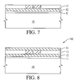
- FIG. 7 is a subsequent cross-sectional view taken from FIG. 6 at a stage of processing subsequent to that shown in FIG. 6 .
- FIG. 8 is a subsequent cross-sectional view taken from FIG. 7 at a stage of processing subsequent to that shown in FIG. 7 .
- FIG. 9A is a subsequent cross-sectional view taken from FIG. 7 at a stage of processing subsequent to that shown in FIG. 7 in accordance with a second embodiment of the invention.
- FIG. 9B is a subsequent cross-sectional view taken from FIG. 9A at a stage of processing subsequent to that shown in FIG. 9A in accordance with the second embodiment of the invention.
- FIG. 9C is a subsequent cross-sectional view taken from FIG. 9B at a stage of processing subsequent to that shown in FIG. 9B in accordance with the second embodiment of the invention.
- FIG. 10 illustrates a process according to an embodiment of the present invention.
- FIG. 11 illustrates an exemplary construction of a resistance variable memory element in accordance with the second embodiment of the invention.
- FIG. 12 is a processor based system having one or more memory devices that contains resistance variable memory elements according to the present invention.
- substrate used in the following description may include any supporting structure including, but not limited to, a plastic or a semiconductor substrate that has an exposed substrate surface.
- Semiconductor substrates should be understood to include silicon, silicon-on-insulator (SOI), silicon-on-sapphire (SOS), doped and undoped semiconductors, epitaxial layers of silicon supported by a base semiconductor foundation, and other semiconductor structures.
- SOI silicon-on-insulator
- SOS silicon-on-sapphire
- doped and undoped semiconductors silicon-on-insulator
- epitaxial layers of silicon supported by a base semiconductor foundation and other semiconductor structures.
- silver is intended to include not only elemental silver, but silver with other trace metals or in various alloyed combinations with other metals as known in the semiconductor industry, as long as such silver alloy is conductive, and as long as the physical and electrical properties of the silver remain unchanged.
- silver-selenide is intended to include various species of silver-selenide, including some species which have a slight excess or deficit of silver, for instance, Ag 2 Se, Ag 2+x Se, and Ag 2 ⁇ x Se.
- semi-volatile memory device is intended to include any memory device which is capable of maintaining its memory state after power is removed from the device for a prolonged period of time. Thus, semi-volatile memory devices are capable of retaining stored data after the power source is disconnected or removed.
- semi-volatile memory device as used herein includes not only semi-volatile memory devices, but also non-volatile memory devices.
- resistance variable memory element is intended to include any memory element, including programmable conductor memory elements, semi-volatile memory elements, and non-volatile memory elements which exhibit a resistance change in response to an applied voltage.
- the present invention relates to a process for forming a resistance variable memory element.
- the invention will now be explained with reference to FIGS. 1–10 , which illustrate exemplary embodiments of a resistance variable memory element 100 in accordance with the invention.
- FIG. 10 shows an exemplary processing sequence for forming a resistance variable memory element in an exemplary embodiment of the invention.
- a semiconductor substrate 10 such as a silicon wafer, is prepared for the processing steps of the present invention.
- a resistance variable memory element may be implemented in various different technologies.
- Insulating material 11 such as silicon dioxide, is formed over substrate 10 in process segment 108 .
- a first electrode 12 is formed over the insulating material 11 .
- the material used to form the electrode can be selected from a variety of conductive materials, for example, tungsten, nickel, tantalum, titanium, titanium nitride, aluminum, platinum, or silver, among many others.
- an insulating layer 13 preferably formed of silicon nitride, is formed over the first electrode 12 .
- This and any other subsequently formed insulating layers may be formed of a conventional insulating nitride or oxide, among others.
- the present invention is not limited, however, to the above-listed materials and other insulating and/or dielectric materials known in the industry may be used.
- the insulating layer may be formed by any known deposition methods, for example, by sputtering, chemical vapor deposition (CVD), plasma enhanced CVD (PECVD) or physical vapor deposition (PVD), among others.
- the insulating layer 13 is etched to form an opening 22 , which exposes the first electrode 12 . This is done by patterning a masking material 21 and etching to remove unmasked portions of the insulating layer 13 , with the etch stopping once it reaches the first electrode 12 .
- the masking material 21 of FIG. 2 is stripped and a metal containing layer 31 , such as silver is formed to substantially fill the opening 22 and contact the first electrode 12 .
- a metal containing layer 31 such as silver is formed to substantially fill the opening 22 and contact the first electrode 12 .
- Silver-selenide may also be used as the metal containing layer 31 .
- the metal containing layer 31 is then planarized down to expose the surface of insulating layer 13 , by using an abrasive planarization etching technique, such as chemical mechanical planarization (CMP).
- CMP chemical mechanical planarization
- a partial etchback preferably a wet etch
- An exemplary wet etch would incorporate HNO 3 and H 2 O.
- Wet etching is preferred to alleviate the problem of a sidewall forming from etch chemicals. Also, as wet etching is performed down an opening, the isotropic nature of wet etching is not a constraint and the etching is self-aligned to the opening.
- a first resistance variable material 41 is formed over the insulating layer 13 and recessed metal containing layer 31 .
- the first resistance variable material 41 is deposited in such a manner so as to contact the recessed metal containing layer 31 .
- the first resistance variable material 41 is a chalcogenide glass and is preferably a germanium-selenide glass.
- the germanium-selenide glass composition is preferably one having a Ge x Se 100 ⁇ x stoichiometry of from about Ge 20 Se 80 to about Ge 33 Se 67 , and is more preferably about Ge 25 Se 75 .
- the first resistance variable material 41 may be deposited by any known deposition methods, for example, by sputtering, chemical vapor deposition (CVD), plasma enhanced CVD (PECVD) or physical vapor deposition (PVD).
- the substrate 10 is either irradiated with light or thermally treated in combination with light irradiation to cause sufficient diffusion of metal ions from recessed metal containing layer 31 into the first resistance variable material 41 .
- the first resistance variable material 41 may be irradiated for about 5 to 30 minutes at between about 1 mW/cm 2 to about 10 mW/cm 2 with light at from about 200 nm to about 600 nm wavelength.
- the irradiation may be used in combination with a thermal process using a temperature of from about 50° C. to about 300° C.
- the irradiation process is sufficient to cause the desired diffusion of metal ions from metal containing layer 31 into layer 41 ; however, the thermal process by itself is not used, but is only used in combination with the irradiation process.
- metal ions are only incorporated into the resistance variable material within the opening 22 .
- metal ions are only incorporated into the resistance variable material within the opening 22 .
- a sufficient amount of the metal containing layer 31 is available for diffusion of metal ions into the resistance variable material 41 .
- any residual resistance variable material over layer 13 is removed by a dry etch process in processing segment 190 shown in FIG. 10 .
- the dry etch process is preferably a chemistry containing a gas which is selective between the resistance variable material 41 and the metal containing resistance variable material 51 .
- an exemplary selective dry etch process would include CF 4 gas and/or SF 6 gas which are selective between Ge 25 Se 75 and Ag x (Ge 25 Se 75 ) 1 ⁇ x .
- the dry etch will not remove it, however, the stress of confining the doped area of the element is relieved through the top of the element resulting in an element that is mushroom shaped at the top of the opening 22 .
- the mushroom shape is not a detriment to electrical performance.
- a second conductive electrode 61 is formed over the insulating layer 13 and metal containing resistance variable material 51 to complete the formation of the resistance variable memory element.
- the second electrode is preferably formed of tungsten, however any suitable conductive materials may be used to form the second electrode 61 .
- the resulting structure forms a resistance variable memory element comprising a metal containing resistance variable material (i.e., such as a silver containing chalcogenide glass layer) and at least two conductive electrodes, namely electrodes 12 and 61 .
- Conventional processing steps can then be carried out to electrically couple the second electrode 61 to various circuits of memory arrays.
- FIGS. 1–8 depict a first exemplary embodiment of the invention.
- the structure depicted in FIG. 7 can also form the base of a second embodiment of the invention.
- the second embodiment is now described with reference to FIGS. 9A–9C and process segments 300 – 320 of FIG. 10 .
- a metal containing layer 71 such as silver-selenide, may be deposited over the metal containing resistance variable material 51 .
- Any suitable metal containing layer 71 may be used.
- other suitable metal containing layers include silver-chalcogenide layers.
- Silver sulfide, silver oxide, and silver telluride are all suitable silver-chalcogenides that may be used in combination with any suitable metal containing resistance variable material 51 .
- a variety of processes can be used to form the metal containing layer 71 .
- physical vapor deposition techniques such as evaporative deposition and sputtering may be used.
- Other processes such as chemical vapor deposition, co-evaporation or depositing a layer of selenium above a layer of silver to form silver-selenide can also be used.
- a second resistance variable material 81 preferably a chalcogenide glass and more preferably a germanium-selenide glass is deposited over the metal containing layer 71 .
- the second germanium-selenide glass composition is preferably one having a Ge x Se 100 ⁇ x stoichiometry between about Ge 20 Se 80 to about Ge 43 Se 57 and is more preferably about Ge 40 Se 60 .
- the second resistance variable material 41 may be deposited by any known deposition methods, for example, by sputtering, chemical vapor deposition (CVD), plasma enhanced CVD (PECVD) or physical vapor deposition (PVD).
- a second conductive electrode 61 is formed over the second resistance variable material 81 to complete the formation of a resistance variable memory element in accordance with the second embodiment of the invention.
- the second electrode is preferably formed of tungsten, however any suitable conductive materials may be used to form the second electrode 61 .
- the resulting structure forms a resistance variable memory element comprising a metal containing resistance variable material 51 (such as a silver-germanium-selenium glass layer), a metal containing layer 71 (such as silver-selenide), a resistance variable material layer 81 (such as a germanium-selenium glass layer), and at least two conductive electrodes, namely electrodes 12 and 61 .
- Conventional processing steps can then be carried out to electrically couple the first and second electrode 12 , 61 to various circuits of memory arrays.
- Providing a metal containing layer 71 , such as silver-selenide, over the metal containing resistance variable material 51 and then providing a second resistance variable material 81 over the metal containing layer 71 allows the metal in the metal containing layer 71 to be more readily available for switching.
- FIG. 11 illustrates an exemplary construction of a resistance variable memory element 100 employing the first embodiment of the invention.
- a resistance variable memory element 100 in accordance with the first embodiment of the invention is generally fabricated over a semiconductor substrate 10 and comprises a first insulating layer 11 formed over a substrate 10 .
- An access transistor 83 for accessing the memory element is illustrated as having source/drain regions 84 , 85 and a gate stack 86 .
- Access circuitry for operating a resistance variable memory cell may be fabricated in substrate 10 .
- the insulating layer 11 is provided over the circuitry, including transistor 83 and contains a conductive plug 161 .
- a first metal electrode 12 is formed within a second insulating layer 8 provided over the insulating layer 11 and plug 161 .
- a third insulating layer 13 is formed over the first electrode 12 and second insulating layer 8 .
- an etched opening is provided.
- a metal material and a resistance variable material are deposited in the opening and processed via light irradiation in accordance with process segments 140 – 190 to form a metal containing resistance variable material 51 in the opening of the third insulating layer 13 .
- the metal containing resistance variable material 51 may be a silver-germanium-selenide glass.
- a second metal electrode 54 is formed in contact with the silver-germanium-selenide glass 51 .
- the third insulating layer 13 may be formed, for example, between the first electrode 12 and the second electrode 54 of any suitable insulator, for example a nitride, an oxide, or other insulator.
- the third insulating layer 13 may be formed by any known deposition method, for example, by sputtering, chemical vapor deposition (CVD), plasma enhanced CVD (PECVD) or physical vapor deposition (PVD), among others.
- a preferred insulating material is silicon nitride, but those skilled in the art will appreciate that there are other numerous suitable insulating materials for this purpose.
- the first electrode 12 is electrically connected through conductive plug 161 to a source/drain region 84 of access transistor 83 .
- Source/drain region 85 is connected by another conductive plug 87 to other circuitry of a memory array.
- the gate of the transistor 83 may be part of a word line which is connected to a plurality of resistance variable memory elements 100 just as a bit line of a memory array may be coupled to a plurality of resistance variable memory elements through plug 87 .
- FIG. 12 illustrates an exemplary processing system 900 which utilizes a resistance variable memory random access device 101 containing an array of resistance variable memory elements 100 constructed as described above with reference to FIGS. 1–10 .
- the processing system 900 includes one or more processors 901 coupled to a local bus 904 .
- a memory controller 902 and a primary bus bridge 903 are also coupled the local bus 904 .
- the processing system 900 may include multiple memory controllers 902 and/or multiple primary bus bridges 903 .
- the memory controller 902 and the primary bus bridge 903 may be integrated as a single device 906 .
- the memory controller 902 is also coupled to one or more memory buses 907 .
- Each memory bus accepts memory components 908 , which include at least one memory device 101 of the invention.
- the memory controller 902 may be omitted and the memory components directly coupled to one or more processors 901 .
- the memory components 908 may be a memory card or a memory module.
- the memory components 908 may include one or more additional devices 909 .
- the additional device 909 might be a configuration memory.
- the memory controller 902 may also be coupled to a cache memory 905 .
- the cache memory 905 may be the only cache memory in the processing system.
- processors 901 may also include cache memories, which may form a cache hierarchy with cache memory 905 .
- the memory controller 902 may implement a cache coherency protocol. If the memory controller 902 is coupled to a plurality of memory buses 907 , each memory bus 907 may be operated in parallel, or different address ranges may be mapped to different memory buses 907 .
- DMA direct memory access
- the primary bus bridge 903 is coupled to at least one peripheral bus 910 .
- Various devices such as peripherals or additional bus bridges may be coupled to the peripheral bus 910 . These devices may include a storage controller 911 , an miscellaneous I/O device 914 , a secondary bus bridge 915 , a multimedia processor 918 , and an legacy device interface 920 .
- the primary bus bridge 903 may also coupled to one or more special purpose high speed ports 922 . In a personal computer, for example, the special purpose port might be the Accelerated Graphics Port (AGP), used to couple a high performance video card to the processing system 900 .
- AGP Accelerated Graphics Port
- the storage controller 911 couples one or more storage devices 913 , via a storage bus 912 , to the peripheral bus 910 .
- the storage controller 911 may be a SCSI controller and storage devices 913 may be SCSI discs.
- the I/O device 914 may be any sort of peripheral.
- the I/O device 914 may be an local area network interface, such as an Ethernet card.
- the secondary bus bridge may be used to interface additional devices via another bus to the processing system.
- the secondary bus bridge may be an universal serial port (USB) controller used to couple USB devices 917 via to the processing system 900 .
- the multimedia processor 918 may be a sound card, a video capture card, or any other type of media interface, which may also be coupled to one additional devices such as speakers 919 .
- the legacy device interface 920 is used to couple legacy devices, for example, older styled keyboards and mice, to the processing system 900 .
- FIG. 12 illustrates a processing architecture especially suitable for a general purpose computer, such as a personal computer or a workstation, it should be recognized that well known modifications can be made to configure the processing system 900 to become more suitable for use in a variety of applications. For example, many electronic devices which require processing may be implemented using a simpler architecture which relies on a CPU 901 coupled to memory components 908 and/or memory elements 100 .
- These electronic devices may include, but are not limited to audio/video processors and recorders, gaming consoles, digital television sets, wired or wireless telephones, navigation devices (including system based on the global positioning system (GPS) and/or inertial navigation), and digital cameras and/or recorders.
- the modifications may include, for example, elimination of unnecessary components, addition of specialized devices or circuits, and/or integration of a plurality of devices.
Abstract
Description
Claims (89)
Priority Applications (3)
| Application Number | Priority Date | Filing Date | Title |
|---|---|---|---|
| US10/225,190 US7018863B2 (en) | 2002-08-22 | 2002-08-22 | Method of manufacture of a resistance variable memory cell |
| US10/886,676 US7459764B2 (en) | 2002-08-22 | 2004-07-09 | Method of manufacture of a PCRAM memory cell |
| US11/430,047 US7550818B2 (en) | 2002-08-22 | 2006-05-09 | Method of manufacture of a PCRAM memory cell |
Applications Claiming Priority (1)
| Application Number | Priority Date | Filing Date | Title |
|---|---|---|---|
| US10/225,190 US7018863B2 (en) | 2002-08-22 | 2002-08-22 | Method of manufacture of a resistance variable memory cell |
Related Child Applications (1)
| Application Number | Title | Priority Date | Filing Date |
|---|---|---|---|
| US10/886,676 Division US7459764B2 (en) | 2002-08-22 | 2004-07-09 | Method of manufacture of a PCRAM memory cell |
Publications (2)
| Publication Number | Publication Date |
|---|---|
| US20040038480A1 US20040038480A1 (en) | 2004-02-26 |
| US7018863B2 true US7018863B2 (en) | 2006-03-28 |
Family
ID=31886964
Family Applications (3)
| Application Number | Title | Priority Date | Filing Date |
|---|---|---|---|
| US10/225,190 Expired - Lifetime US7018863B2 (en) | 2002-08-22 | 2002-08-22 | Method of manufacture of a resistance variable memory cell |
| US10/886,676 Expired - Lifetime US7459764B2 (en) | 2002-08-22 | 2004-07-09 | Method of manufacture of a PCRAM memory cell |
| US11/430,047 Expired - Lifetime US7550818B2 (en) | 2002-08-22 | 2006-05-09 | Method of manufacture of a PCRAM memory cell |
Family Applications After (2)
| Application Number | Title | Priority Date | Filing Date |
|---|---|---|---|
| US10/886,676 Expired - Lifetime US7459764B2 (en) | 2002-08-22 | 2004-07-09 | Method of manufacture of a PCRAM memory cell |
| US11/430,047 Expired - Lifetime US7550818B2 (en) | 2002-08-22 | 2006-05-09 | Method of manufacture of a PCRAM memory cell |
Country Status (1)
| Country | Link |
|---|---|
| US (3) | US7018863B2 (en) |
Cited By (13)
| Publication number | Priority date | Publication date | Assignee | Title |
|---|---|---|---|---|
| US20060045974A1 (en) * | 2004-08-25 | 2006-03-02 | Campbell Kristy A | Wet chemical method to form silver-rich silver-selenide |
| US20060076413A1 (en) * | 2004-08-27 | 2006-04-13 | Infineon Technologies Ag | Chip card and chip card security device |
| US20060121391A1 (en) * | 2004-12-02 | 2006-06-08 | Yoon-Ho Khang | Phase change memory device having phase change material layer containing phase change nano particles and method of fabricating the same |
| KR100785032B1 (en) | 2006-11-29 | 2007-12-12 | 삼성전자주식회사 | Resistive random access memory device and method of manufacuring the same |
| US20080073638A1 (en) * | 2006-08-25 | 2008-03-27 | Micron Technology, Inc. | Programmable resistance memory devices and systems using the same and methods of forming the same |
| US20080121859A1 (en) * | 2006-10-19 | 2008-05-29 | Boise State University | Forced ion migration for chalcogenide phase change memory device |
| US20100027324A1 (en) * | 2008-08-01 | 2010-02-04 | Boise State University | Variable integrated analog resistor |
| US20100090749A1 (en) * | 2008-10-09 | 2010-04-15 | United Microelectronics Corp. | Multi-function chip |
| US20110079709A1 (en) * | 2009-10-07 | 2011-04-07 | Campbell Kristy A | Wide band sensor |
| US8049202B2 (en) | 2004-12-02 | 2011-11-01 | Samsung Electronics Co., Ltd. | Phase change memory device having phase change material layer containing phase change nano particles |
| US8284590B2 (en) | 2010-05-06 | 2012-10-09 | Boise State University | Integratable programmable capacitive device |
| US8467236B2 (en) | 2008-08-01 | 2013-06-18 | Boise State University | Continuously variable resistor |
| US10319908B2 (en) * | 2014-05-01 | 2019-06-11 | Crossbar, Inc. | Integrative resistive memory in backend metal layers |
Families Citing this family (13)
| Publication number | Priority date | Publication date | Assignee | Title |
|---|---|---|---|---|
| US6881623B2 (en) * | 2001-08-29 | 2005-04-19 | Micron Technology, Inc. | Method of forming chalcogenide comprising devices, method of forming a programmable memory cell of memory circuitry, and a chalcogenide comprising device |
| US6815266B2 (en) * | 2002-12-30 | 2004-11-09 | Bae Systems Information And Electronic Systems Integration, Inc. | Method for manufacturing sidewall contacts for a chalcogenide memory device |
| US20050287698A1 (en) * | 2004-06-28 | 2005-12-29 | Zhiyong Li | Use of chalcogen plasma to form chalcogenide switching materials for nanoscale electronic devices |
| WO2006069082A2 (en) * | 2004-12-20 | 2006-06-29 | Bionopoly Llc | Access keys |
| DE102005012047A1 (en) * | 2005-03-16 | 2006-09-28 | Infineon Technologies Ag | Solid-state electrolyte memory manufacture involves coating first electrode with solid-state electrolyte layer, and then forming second electrode on solid-state electrolyte layer |
| US7579615B2 (en) * | 2005-08-09 | 2009-08-25 | Micron Technology, Inc. | Access transistor for memory device |
| JP4492816B2 (en) * | 2006-10-03 | 2010-06-30 | 株式会社半導体理工学研究センター | Multilevel recording phase change memory device, multilevel recording phase change channel transistor, and memory cell array |
| US7718533B2 (en) * | 2007-05-08 | 2010-05-18 | Micron Technology, Inc. | Inverted variable resistance memory cell and method of making the same |
| KR20090090563A (en) * | 2008-02-21 | 2009-08-26 | 삼성전자주식회사 | Semiconductor devices having resistive memory element |
| US8064247B2 (en) * | 2009-01-14 | 2011-11-22 | Macronix International Co., Ltd. | Rewritable memory device based on segregation/re-absorption |
| US8685783B2 (en) | 2010-10-27 | 2014-04-01 | Taiwan Semiconductor Manufacturing Company, Ltd. | Phase change memory cell |
| US9219020B2 (en) * | 2012-03-08 | 2015-12-22 | Infineon Technologies Ag | Semiconductor device, wafer assembly and methods of manufacturing wafer assemblies and semiconductor devices |
| US10693062B2 (en) * | 2015-12-08 | 2020-06-23 | Crossbar, Inc. | Regulating interface layer formation for two-terminal memory |
Citations (96)
| Publication number | Priority date | Publication date | Assignee | Title |
|---|---|---|---|---|
| US3271591A (en) | 1963-09-20 | 1966-09-06 | Energy Conversion Devices Inc | Symmetrical current controlling device |
| US3622319A (en) | 1966-10-20 | 1971-11-23 | Western Electric Co | Nonreflecting photomasks and methods of making same |
| US3743847A (en) | 1971-06-01 | 1973-07-03 | Motorola Inc | Amorphous silicon film as a uv filter |
| US3961314A (en) | 1974-03-05 | 1976-06-01 | Energy Conversion Devices, Inc. | Structure and method for producing an image |
| US3966317A (en) | 1974-04-08 | 1976-06-29 | Energy Conversion Devices, Inc. | Dry process production of archival microform records from hard copy |
| US3983542A (en) | 1970-08-13 | 1976-09-28 | Energy Conversion Devices, Inc. | Method and apparatus for recording information |
| US4177474A (en) | 1977-05-18 | 1979-12-04 | Energy Conversion Devices, Inc. | High temperature amorphous semiconductor member and method of making the same |
| US4267261A (en) | 1971-07-15 | 1981-05-12 | Energy Conversion Devices, Inc. | Method for full format imaging |
| US4269935A (en) | 1979-07-13 | 1981-05-26 | Ionomet Company, Inc. | Process of doping silver image in chalcogenide layer |
| US4312938A (en) | 1979-07-06 | 1982-01-26 | Drexler Technology Corporation | Method for making a broadband reflective laser recording and data storage medium with absorptive underlayer |
| US4316946A (en) | 1979-12-03 | 1982-02-23 | Ionomet Company, Inc. | Surface sensitized chalcogenide product and process for making and using the same |
| US4320191A (en) | 1978-11-07 | 1982-03-16 | Nippon Telegraph & Telephone Public Corporation | Pattern-forming process |
| US4405710A (en) | 1981-06-22 | 1983-09-20 | Cornell Research Foundation, Inc. | Ion beam exposure of (g-Gex -Se1-x) inorganic resists |
| US4419421A (en) | 1979-01-15 | 1983-12-06 | Max-Planck-Gesellschaft Zur Forderung Der Wissenschaften E.V. | Ion conductor material |
| US4499557A (en) | 1980-10-28 | 1985-02-12 | Energy Conversion Devices, Inc. | Programmable cell for use in programmable electronic arrays |
| US4597162A (en) | 1983-01-18 | 1986-07-01 | Energy Conversion Devices, Inc. | Method for making, parallel preprogramming or field programming of electronic matrix arrays |
| US4608296A (en) | 1983-12-06 | 1986-08-26 | Energy Conversion Devices, Inc. | Superconducting films and devices exhibiting AC to DC conversion |
| US4637895A (en) | 1985-04-01 | 1987-01-20 | Energy Conversion Devices, Inc. | Gas mixtures for the vapor deposition of semiconductor material |
| US4646266A (en) | 1984-09-28 | 1987-02-24 | Energy Conversion Devices, Inc. | Programmable semiconductor structures and methods for using the same |
| US4664939A (en) | 1985-04-01 | 1987-05-12 | Energy Conversion Devices, Inc. | Vertical semiconductor processor |
| US4668968A (en) | 1984-05-14 | 1987-05-26 | Energy Conversion Devices, Inc. | Integrated circuit compatible thin film field effect transistor and method of making same |
| US4670763A (en) | 1984-05-14 | 1987-06-02 | Energy Conversion Devices, Inc. | Thin film field effect transistor |
| US4671618A (en) | 1986-05-22 | 1987-06-09 | Wu Bao Gang | Liquid crystalline-plastic material having submillisecond switch times and extended memory |
| US4673957A (en) | 1984-05-14 | 1987-06-16 | Energy Conversion Devices, Inc. | Integrated circuit compatible thin film field effect transistor and method of making same |
| US4678679A (en) | 1984-06-25 | 1987-07-07 | Energy Conversion Devices, Inc. | Continuous deposition of activated process gases |
| US4710899A (en) | 1985-06-10 | 1987-12-01 | Energy Conversion Devices, Inc. | Data storage medium incorporating a transition metal for increased switching speed |
| US4728406A (en) | 1986-08-18 | 1988-03-01 | Energy Conversion Devices, Inc. | Method for plasma - coating a semiconductor body |
| US4737379A (en) | 1982-09-24 | 1988-04-12 | Energy Conversion Devices, Inc. | Plasma deposited coatings, and low temperature plasma method of making same |
| US4766471A (en) | 1986-01-23 | 1988-08-23 | Energy Conversion Devices, Inc. | Thin film electro-optical devices |
| US4769338A (en) | 1984-05-14 | 1988-09-06 | Energy Conversion Devices, Inc. | Thin film field effect transistor and method of making same |
| US4775425A (en) | 1987-07-27 | 1988-10-04 | Energy Conversion Devices, Inc. | P and n-type microcrystalline semiconductor alloy material including band gap widening elements, devices utilizing same |
| US4788594A (en) | 1986-10-15 | 1988-11-29 | Energy Conversion Devices, Inc. | Solid state electronic camera including thin film matrix of photosensors |
| US4795657A (en) | 1984-04-13 | 1989-01-03 | Energy Conversion Devices, Inc. | Method of fabricating a programmable array |
| US4800526A (en) | 1987-05-08 | 1989-01-24 | Gaf Corporation | Memory element for information storage and retrieval system and associated process |
| US4804490A (en) | 1987-10-13 | 1989-02-14 | Energy Conversion Devices, Inc. | Method of fabricating stabilized threshold switching material |
| US4809044A (en) | 1986-08-22 | 1989-02-28 | Energy Conversion Devices, Inc. | Thin film overvoltage protection devices |
| US4818717A (en) | 1986-06-27 | 1989-04-04 | Energy Conversion Devices, Inc. | Method for making electronic matrix arrays |
| US4843443A (en) | 1984-05-14 | 1989-06-27 | Energy Conversion Devices, Inc. | Thin film field effect transistor and method of making same |
| US4845533A (en) | 1986-08-22 | 1989-07-04 | Energy Conversion Devices, Inc. | Thin film electrical devices with amorphous carbon electrodes and method of making same |
| US4847674A (en) | 1987-03-10 | 1989-07-11 | Advanced Micro Devices, Inc. | High speed interconnect system with refractory non-dogbone contacts and an active electromigration suppression mechanism |
| US4853785A (en) | 1986-10-15 | 1989-08-01 | Energy Conversion Devices, Inc. | Electronic camera including electronic signal storage cartridge |
| US4891330A (en) | 1987-07-27 | 1990-01-02 | Energy Conversion Devices, Inc. | Method of fabricating n-type and p-type microcrystalline semiconductor alloy material including band gap widening elements |
| US4920078A (en) | 1989-06-02 | 1990-04-24 | Bell Communications Research, Inc. | Arsenic sulfide surface passivation of III-V semiconductors |
| US5128099A (en) | 1991-02-15 | 1992-07-07 | Energy Conversion Devices, Inc. | Congruent state changeable optical memory material and device |
| US5159661A (en) | 1990-10-05 | 1992-10-27 | Energy Conversion Devices, Inc. | Vertically interconnected parallel distributed processor |
| US5166758A (en) | 1991-01-18 | 1992-11-24 | Energy Conversion Devices, Inc. | Electrically erasable phase change memory |
| US5177567A (en) | 1991-07-19 | 1993-01-05 | Energy Conversion Devices, Inc. | Thin-film structure for chalcogenide electrical switching devices and process therefor |
| US5219788A (en) | 1991-02-25 | 1993-06-15 | Ibm Corporation | Bilayer metallization cap for photolithography |
| US5238862A (en) | 1992-03-18 | 1993-08-24 | Micron Technology, Inc. | Method of forming a stacked capacitor with striated electrode |
| US5272359A (en) | 1988-04-07 | 1993-12-21 | California Institute Of Technology | Reversible non-volatile switch based on a TCNQ charge transfer complex |
| US5296716A (en) | 1991-01-18 | 1994-03-22 | Energy Conversion Devices, Inc. | Electrically erasable, directly overwritable, multibit single cell memory elements and arrays fabricated therefrom |
| US5314772A (en) | 1990-10-09 | 1994-05-24 | Arizona Board Of Regents | High resolution, multi-layer resist for microlithography and method therefor |
| US5315131A (en) | 1990-11-22 | 1994-05-24 | Matsushita Electric Industrial Co., Ltd. | Electrically reprogrammable nonvolatile memory device |
| US5330630A (en) | 1991-01-02 | 1994-07-19 | Energy Conversion Devices, Inc. | Switch with improved threshold voltage |
| US5335219A (en) | 1991-01-18 | 1994-08-02 | Ovshinsky Stanford R | Homogeneous composition of microcrystalline semiconductor material, semiconductor devices and directly overwritable memory elements fabricated therefrom, and arrays fabricated from the memory elements |
| US5341328A (en) | 1991-01-18 | 1994-08-23 | Energy Conversion Devices, Inc. | Electrically erasable memory elements having reduced switching current requirements and increased write/erase cycle life |
| US5350484A (en) | 1992-09-08 | 1994-09-27 | Intel Corporation | Method for the anisotropic etching of metal films in the fabrication of interconnects |
| US5359205A (en) | 1991-11-07 | 1994-10-25 | Energy Conversion Devices, Inc. | Electrically erasable memory elements characterized by reduced current and improved thermal stability |
| US5360981A (en) | 1989-05-11 | 1994-11-01 | British Telecommunications Public Limited Company | Amorphous silicon memory |
| US5406509A (en) | 1991-01-18 | 1995-04-11 | Energy Conversion Devices, Inc. | Electrically erasable, directly overwritable, multibit single cell memory elements and arrays fabricated therefrom |
| US5414271A (en) | 1991-01-18 | 1995-05-09 | Energy Conversion Devices, Inc. | Electrically erasable memory elements having improved set resistance stability |
| US5500532A (en) | 1994-08-18 | 1996-03-19 | Arizona Board Of Regents | Personal electronic dosimeter |
| US5512773A (en) | 1993-12-23 | 1996-04-30 | U.S. Philips Corporation | Switching element with memory provided with Schottky tunnelling barrier |
| US5512328A (en) | 1992-08-07 | 1996-04-30 | Hitachi, Ltd. | Method for forming a pattern and forming a thin film used in pattern formation |
| US5534711A (en) | 1991-01-18 | 1996-07-09 | Energy Conversion Devices, Inc. | Electrically erasable, directly overwritable, multibit single cell memory elements and arrays fabricated therefrom |
| US5534712A (en) | 1991-01-18 | 1996-07-09 | Energy Conversion Devices, Inc. | Electrically erasable memory elements characterized by reduced current and improved thermal stability |
| US5536947A (en) | 1991-01-18 | 1996-07-16 | Energy Conversion Devices, Inc. | Electrically erasable, directly overwritable, multibit single cell memory element and arrays fabricated therefrom |
| US5543737A (en) | 1995-02-10 | 1996-08-06 | Energy Conversion Devices, Inc. | Logical operation circuit employing two-terminal chalcogenide switches |
| US5591501A (en) | 1995-12-20 | 1997-01-07 | Energy Conversion Devices, Inc. | Optical recording medium having a plurality of discrete phase change data recording points |
| US5596522A (en) | 1991-01-18 | 1997-01-21 | Energy Conversion Devices, Inc. | Homogeneous compositions of microcrystalline semiconductor material, semiconductor devices and directly overwritable memory elements fabricated therefrom, and arrays fabricated from the memory elements |
| US5687112A (en) | 1996-04-19 | 1997-11-11 | Energy Conversion Devices, Inc. | Multibit single cell memory element having tapered contact |
| US5694054A (en) | 1995-11-28 | 1997-12-02 | Energy Conversion Devices, Inc. | Integrated drivers for flat panel displays employing chalcogenide logic elements |
| US5714768A (en) | 1995-10-24 | 1998-02-03 | Energy Conversion Devices, Inc. | Second-layer phase change memory array on top of a logic device |
| US5726083A (en) | 1994-11-29 | 1998-03-10 | Nec Corporation | Process of fabricating dynamic random access memory device having storage capacitor low in contact resistance and small in leakage current through tantalum oxide film |
| US5751012A (en) | 1995-06-07 | 1998-05-12 | Micron Technology, Inc. | Polysilicon pillar diode for use in a non-volatile memory cell |
| US5761115A (en) * | 1996-05-30 | 1998-06-02 | Axon Technologies Corporation | Programmable metallization cell structure and method of making same |
| US5789277A (en) | 1996-07-22 | 1998-08-04 | Micron Technology, Inc. | Method of making chalogenide memory device |
| US5814527A (en) | 1996-07-22 | 1998-09-29 | Micron Technology, Inc. | Method of making small pores defined by a disposable internal spacer for use in chalcogenide memories |
| US5818749A (en) | 1993-08-20 | 1998-10-06 | Micron Technology, Inc. | Integrated circuit memory device |
| US5825046A (en) | 1996-10-28 | 1998-10-20 | Energy Conversion Devices, Inc. | Composite memory material comprising a mixture of phase-change memory material and dielectric material |
| US5837564A (en) | 1995-11-01 | 1998-11-17 | Micron Technology, Inc. | Method for optimal crystallization to obtain high electrical performance from chalcogenides |
| US5841150A (en) | 1995-06-07 | 1998-11-24 | Micron Technology, Inc. | Stack/trench diode for use with a muti-state material in a non-volatile memory cell |
| US5846889A (en) | 1997-03-14 | 1998-12-08 | The United States Of America As Represented By The Secretary Of The Navy | Infrared transparent selenide glasses |
| US5851882A (en) | 1996-05-06 | 1998-12-22 | Micron Technology, Inc. | ZPROM manufacture and design and methods for forming thin structures using spacers as an etching mask |
| US5869843A (en) | 1995-06-07 | 1999-02-09 | Micron Technology, Inc. | Memory array having a multi-state element and method for forming such array or cells thereof |
| US5912839A (en) | 1998-06-23 | 1999-06-15 | Energy Conversion Devices, Inc. | Universal memory element and method of programming same |
| US5920788A (en) | 1995-06-07 | 1999-07-06 | Micron Technology, Inc. | Chalcogenide memory cell with a plurality of chalcogenide electrodes |
| US5933365A (en) | 1997-06-19 | 1999-08-03 | Energy Conversion Devices, Inc. | Memory element with energy control mechanism |
| US5998066A (en) | 1997-05-16 | 1999-12-07 | Aerial Imaging Corporation | Gray scale mask and depth pattern transfer technique using inorganic chalcogenide glass |
| US6011757A (en) | 1998-01-27 | 2000-01-04 | Ovshinsky; Stanford R. | Optical recording media having increased erasability |
| US6031287A (en) | 1997-06-18 | 2000-02-29 | Micron Technology, Inc. | Contact structure and memory element incorporating the same |
| US6072716A (en) | 1999-04-14 | 2000-06-06 | Massachusetts Institute Of Technology | Memory structures and methods of making same |
| US6087674A (en) | 1996-10-28 | 2000-07-11 | Energy Conversion Devices, Inc. | Memory element with memory material comprising phase-change material and dielectric material |
| US6348365B1 (en) * | 2001-03-02 | 2002-02-19 | Micron Technology, Inc. | PCRAM cell manufacturing |
| US6418049B1 (en) * | 1997-12-04 | 2002-07-09 | Arizona Board Of Regents | Programmable sub-surface aggregating metallization structure and method of making same |
| US6818481B2 (en) * | 2001-03-07 | 2004-11-16 | Micron Technology, Inc. | Method to manufacture a buried electrode PCRAM cell |
Family Cites Families (54)
| Publication number | Priority date | Publication date | Assignee | Title |
|---|---|---|---|---|
| US449557A (en) * | 1891-03-31 | Plumb-level | ||
| US650111A (en) * | 1899-08-31 | 1900-05-22 | Eclipse Automobile Company | Steam-reheater. |
| US5479319A (en) * | 1992-12-30 | 1995-12-26 | Interconnect Systems, Inc. | Multi-level assemblies for interconnecting integrated circuits |
| US6420725B1 (en) | 1995-06-07 | 2002-07-16 | Micron Technology, Inc. | Method and apparatus for forming an integrated circuit electrode having a reduced contact area |
| US5879955A (en) * | 1995-06-07 | 1999-03-09 | Micron Technology, Inc. | Method for fabricating an array of ultra-small pores for chalcogenide memory cells |
| US6653733B1 (en) * | 1996-02-23 | 2003-11-25 | Micron Technology, Inc. | Conductors in semiconductor devices |
| US5998244A (en) * | 1996-08-22 | 1999-12-07 | Micron Technology, Inc. | Memory cell incorporating a chalcogenide element and method of making same |
| US6141241A (en) | 1998-06-23 | 2000-10-31 | Energy Conversion Devices, Inc. | Universal memory element with systems employing same and apparatus and method for reading, writing and programming same |
| US6388324B2 (en) * | 1998-08-31 | 2002-05-14 | Arizona Board Of Regents | Self-repairing interconnections for electrical circuits |
| US6825489B2 (en) * | 2001-04-06 | 2004-11-30 | Axon Technologies Corporation | Microelectronic device, structure, and system, including a memory structure having a variable programmable property and method of forming the same |
| US6487106B1 (en) * | 1999-01-12 | 2002-11-26 | Arizona Board Of Regents | Programmable microelectronic devices and method of forming and programming same |
| US6177338B1 (en) * | 1999-02-08 | 2001-01-23 | Taiwan Semiconductor Manufacturing Company | Two step barrier process |
| US6143604A (en) | 1999-06-04 | 2000-11-07 | Taiwan Semiconductor Manufacturing Company | Method for fabricating small-size two-step contacts for word-line strapping on dynamic random access memory (DRAM) |
| US6350679B1 (en) * | 1999-08-03 | 2002-02-26 | Micron Technology, Inc. | Methods of providing an interlevel dielectric layer intermediate different elevation conductive metal layers in the fabrication of integrated circuitry |
| US6914802B2 (en) * | 2000-02-11 | 2005-07-05 | Axon Technologies Corporation | Microelectronic photonic structure and device and method of forming the same |
| US6339544B1 (en) * | 2000-09-29 | 2002-01-15 | Intel Corporation | Method to enhance performance of thermal resistor device |
| US6563164B2 (en) * | 2000-09-29 | 2003-05-13 | Ovonyx, Inc. | Compositionally modified resistive electrode |
| US6555860B2 (en) * | 2000-09-29 | 2003-04-29 | Intel Corporation | Compositionally modified resistive electrode |
| US6567293B1 (en) * | 2000-09-29 | 2003-05-20 | Ovonyx, Inc. | Single level metal memory cell using chalcogenide cladding |
| US6653193B2 (en) * | 2000-12-08 | 2003-11-25 | Micron Technology, Inc. | Resistance variable device |
| US6696355B2 (en) * | 2000-12-14 | 2004-02-24 | Ovonyx, Inc. | Method to selectively increase the top resistance of the lower programming electrode in a phase-change memory |
| US6569705B2 (en) * | 2000-12-21 | 2003-05-27 | Intel Corporation | Metal structure for a phase-change memory device |
| US6534781B2 (en) * | 2000-12-26 | 2003-03-18 | Ovonyx, Inc. | Phase-change memory bipolar array utilizing a single shallow trench isolation for creating an individual active area region for two memory array elements and one bipolar base contact |
| US6531373B2 (en) * | 2000-12-27 | 2003-03-11 | Ovonyx, Inc. | Method of forming a phase-change memory cell using silicon on insulator low electrode in charcogenide elements |
| US6687427B2 (en) * | 2000-12-29 | 2004-02-03 | Intel Corporation | Optic switch |
| US6727192B2 (en) * | 2001-03-01 | 2004-04-27 | Micron Technology, Inc. | Methods of metal doping a chalcogenide material |
| US6734455B2 (en) * | 2001-03-15 | 2004-05-11 | Micron Technology, Inc. | Agglomeration elimination for metal sputter deposition of chalcogenides |
| US7102150B2 (en) * | 2001-05-11 | 2006-09-05 | Harshfield Steven T | PCRAM memory cell and method of making same |
| US6570784B2 (en) * | 2001-06-29 | 2003-05-27 | Ovonyx, Inc. | Programming a phase-change material memory |
| US6511862B2 (en) * | 2001-06-30 | 2003-01-28 | Ovonyx, Inc. | Modified contact for programmable devices |
| US6514805B2 (en) * | 2001-06-30 | 2003-02-04 | Intel Corporation | Trench sidewall profile for device isolation |
| US6673700B2 (en) * | 2001-06-30 | 2004-01-06 | Ovonyx, Inc. | Reduced area intersection between electrode and programming element |
| US6511867B2 (en) * | 2001-06-30 | 2003-01-28 | Ovonyx, Inc. | Utilizing atomic layer deposition for programmable device |
| US6951805B2 (en) * | 2001-08-01 | 2005-10-04 | Micron Technology, Inc. | Method of forming integrated circuitry, method of forming memory circuitry, and method of forming random access memory circuitry |
| US6590807B2 (en) * | 2001-08-02 | 2003-07-08 | Intel Corporation | Method for reading a structural phase-change memory |
| US6737312B2 (en) * | 2001-08-27 | 2004-05-18 | Micron Technology, Inc. | Method of fabricating dual PCRAM cells sharing a common electrode |
| US6881623B2 (en) * | 2001-08-29 | 2005-04-19 | Micron Technology, Inc. | Method of forming chalcogenide comprising devices, method of forming a programmable memory cell of memory circuitry, and a chalcogenide comprising device |
| US6784018B2 (en) * | 2001-08-29 | 2004-08-31 | Micron Technology, Inc. | Method of forming chalcogenide comprising devices and method of forming a programmable memory cell of memory circuitry |
| US6955940B2 (en) * | 2001-08-29 | 2005-10-18 | Micron Technology, Inc. | Method of forming chalcogenide comprising devices |
| US20030047765A1 (en) * | 2001-08-30 | 2003-03-13 | Campbell Kristy A. | Stoichiometry for chalcogenide glasses useful for memory devices and method of formation |
| US6709958B2 (en) * | 2001-08-30 | 2004-03-23 | Micron Technology, Inc. | Integrated circuit device and fabrication using metal-doped chalcogenide materials |
| US6646902B2 (en) * | 2001-08-30 | 2003-11-11 | Micron Technology, Inc. | Method of retaining memory state in a programmable conductor RAM |
| US6507061B1 (en) * | 2001-08-31 | 2003-01-14 | Intel Corporation | Multiple layer phase-change memory |
| US7113474B2 (en) * | 2001-09-01 | 2006-09-26 | Energy Conversion Devices, Inc. | Increased data storage in optical data storage and retrieval systems using blue lasers and/or plasmon lenses |
| US6545287B2 (en) * | 2001-09-07 | 2003-04-08 | Intel Corporation | Using selective deposition to form phase-change memory cells |
| US6690026B2 (en) * | 2001-09-28 | 2004-02-10 | Intel Corporation | Method of fabricating a three-dimensional array of active media |
| US6566700B2 (en) * | 2001-10-11 | 2003-05-20 | Ovonyx, Inc. | Carbon-containing interfacial layer for phase-change memory |
| US6545907B1 (en) * | 2001-10-30 | 2003-04-08 | Ovonyx, Inc. | Technique and apparatus for performing write operations to a phase change material memory device |
| US6576921B2 (en) * | 2001-11-08 | 2003-06-10 | Intel Corporation | Isolating phase change material memory cells |
| US6815818B2 (en) * | 2001-11-19 | 2004-11-09 | Micron Technology, Inc. | Electrode structure for use in an integrated circuit |
| US6791859B2 (en) * | 2001-11-20 | 2004-09-14 | Micron Technology, Inc. | Complementary bit PCRAM sense amplifier and method of operation |
| US6512241B1 (en) * | 2001-12-31 | 2003-01-28 | Intel Corporation | Phase change material memory device |
| US6671710B2 (en) * | 2002-05-10 | 2003-12-30 | Energy Conversion Devices, Inc. | Methods of computing with digital multistate phase change materials |
| US6918382B2 (en) * | 2002-08-26 | 2005-07-19 | Energy Conversion Devices, Inc. | Hydrogen powered scooter |
-
2002
- 2002-08-22 US US10/225,190 patent/US7018863B2/en not_active Expired - Lifetime
-
2004
- 2004-07-09 US US10/886,676 patent/US7459764B2/en not_active Expired - Lifetime
-
2006
- 2006-05-09 US US11/430,047 patent/US7550818B2/en not_active Expired - Lifetime
Patent Citations (103)
| Publication number | Priority date | Publication date | Assignee | Title |
|---|---|---|---|---|
| US3271591A (en) | 1963-09-20 | 1966-09-06 | Energy Conversion Devices Inc | Symmetrical current controlling device |
| US3622319A (en) | 1966-10-20 | 1971-11-23 | Western Electric Co | Nonreflecting photomasks and methods of making same |
| US3983542A (en) | 1970-08-13 | 1976-09-28 | Energy Conversion Devices, Inc. | Method and apparatus for recording information |
| US3988720A (en) | 1970-08-13 | 1976-10-26 | Energy Conversion Devices, Inc. | Recording and retrieving information in an amorphous memory material using a catalytic material |
| US3743847A (en) | 1971-06-01 | 1973-07-03 | Motorola Inc | Amorphous silicon film as a uv filter |
| US4267261A (en) | 1971-07-15 | 1981-05-12 | Energy Conversion Devices, Inc. | Method for full format imaging |
| US3961314A (en) | 1974-03-05 | 1976-06-01 | Energy Conversion Devices, Inc. | Structure and method for producing an image |
| US3966317A (en) | 1974-04-08 | 1976-06-29 | Energy Conversion Devices, Inc. | Dry process production of archival microform records from hard copy |
| US4177474A (en) | 1977-05-18 | 1979-12-04 | Energy Conversion Devices, Inc. | High temperature amorphous semiconductor member and method of making the same |
| US4320191A (en) | 1978-11-07 | 1982-03-16 | Nippon Telegraph & Telephone Public Corporation | Pattern-forming process |
| US4419421A (en) | 1979-01-15 | 1983-12-06 | Max-Planck-Gesellschaft Zur Forderung Der Wissenschaften E.V. | Ion conductor material |
| US4312938A (en) | 1979-07-06 | 1982-01-26 | Drexler Technology Corporation | Method for making a broadband reflective laser recording and data storage medium with absorptive underlayer |
| US4269935A (en) | 1979-07-13 | 1981-05-26 | Ionomet Company, Inc. | Process of doping silver image in chalcogenide layer |
| US4316946A (en) | 1979-12-03 | 1982-02-23 | Ionomet Company, Inc. | Surface sensitized chalcogenide product and process for making and using the same |
| US4499557A (en) | 1980-10-28 | 1985-02-12 | Energy Conversion Devices, Inc. | Programmable cell for use in programmable electronic arrays |
| US4405710A (en) | 1981-06-22 | 1983-09-20 | Cornell Research Foundation, Inc. | Ion beam exposure of (g-Gex -Se1-x) inorganic resists |
| US4737379A (en) | 1982-09-24 | 1988-04-12 | Energy Conversion Devices, Inc. | Plasma deposited coatings, and low temperature plasma method of making same |
| US4597162A (en) | 1983-01-18 | 1986-07-01 | Energy Conversion Devices, Inc. | Method for making, parallel preprogramming or field programming of electronic matrix arrays |
| US4608296A (en) | 1983-12-06 | 1986-08-26 | Energy Conversion Devices, Inc. | Superconducting films and devices exhibiting AC to DC conversion |
| US4795657A (en) | 1984-04-13 | 1989-01-03 | Energy Conversion Devices, Inc. | Method of fabricating a programmable array |
| US4673957A (en) | 1984-05-14 | 1987-06-16 | Energy Conversion Devices, Inc. | Integrated circuit compatible thin film field effect transistor and method of making same |
| US4668968A (en) | 1984-05-14 | 1987-05-26 | Energy Conversion Devices, Inc. | Integrated circuit compatible thin film field effect transistor and method of making same |
| US4670763A (en) | 1984-05-14 | 1987-06-02 | Energy Conversion Devices, Inc. | Thin film field effect transistor |
| US4843443A (en) | 1984-05-14 | 1989-06-27 | Energy Conversion Devices, Inc. | Thin film field effect transistor and method of making same |
| US4769338A (en) | 1984-05-14 | 1988-09-06 | Energy Conversion Devices, Inc. | Thin film field effect transistor and method of making same |
| US4678679A (en) | 1984-06-25 | 1987-07-07 | Energy Conversion Devices, Inc. | Continuous deposition of activated process gases |
| US4646266A (en) | 1984-09-28 | 1987-02-24 | Energy Conversion Devices, Inc. | Programmable semiconductor structures and methods for using the same |
| US4664939A (en) | 1985-04-01 | 1987-05-12 | Energy Conversion Devices, Inc. | Vertical semiconductor processor |
| US4637895A (en) | 1985-04-01 | 1987-01-20 | Energy Conversion Devices, Inc. | Gas mixtures for the vapor deposition of semiconductor material |
| US4696758A (en) | 1985-04-01 | 1987-09-29 | Energy Conversion Devices, Inc. | Gas mixtures for the vapor deposition of semiconductor material |
| US4698234A (en) | 1985-04-01 | 1987-10-06 | Energy Conversion Devices, Inc. | Vapor deposition of semiconductor material |
| US4710899A (en) | 1985-06-10 | 1987-12-01 | Energy Conversion Devices, Inc. | Data storage medium incorporating a transition metal for increased switching speed |
| US4766471A (en) | 1986-01-23 | 1988-08-23 | Energy Conversion Devices, Inc. | Thin film electro-optical devices |
| US4671618A (en) | 1986-05-22 | 1987-06-09 | Wu Bao Gang | Liquid crystalline-plastic material having submillisecond switch times and extended memory |
| US4818717A (en) | 1986-06-27 | 1989-04-04 | Energy Conversion Devices, Inc. | Method for making electronic matrix arrays |
| US4728406A (en) | 1986-08-18 | 1988-03-01 | Energy Conversion Devices, Inc. | Method for plasma - coating a semiconductor body |
| US4845533A (en) | 1986-08-22 | 1989-07-04 | Energy Conversion Devices, Inc. | Thin film electrical devices with amorphous carbon electrodes and method of making same |
| US4809044A (en) | 1986-08-22 | 1989-02-28 | Energy Conversion Devices, Inc. | Thin film overvoltage protection devices |
| US4788594A (en) | 1986-10-15 | 1988-11-29 | Energy Conversion Devices, Inc. | Solid state electronic camera including thin film matrix of photosensors |
| US4853785A (en) | 1986-10-15 | 1989-08-01 | Energy Conversion Devices, Inc. | Electronic camera including electronic signal storage cartridge |
| US4847674A (en) | 1987-03-10 | 1989-07-11 | Advanced Micro Devices, Inc. | High speed interconnect system with refractory non-dogbone contacts and an active electromigration suppression mechanism |
| US4800526A (en) | 1987-05-08 | 1989-01-24 | Gaf Corporation | Memory element for information storage and retrieval system and associated process |
| US4891330A (en) | 1987-07-27 | 1990-01-02 | Energy Conversion Devices, Inc. | Method of fabricating n-type and p-type microcrystalline semiconductor alloy material including band gap widening elements |
| US4775425A (en) | 1987-07-27 | 1988-10-04 | Energy Conversion Devices, Inc. | P and n-type microcrystalline semiconductor alloy material including band gap widening elements, devices utilizing same |
| US4804490A (en) | 1987-10-13 | 1989-02-14 | Energy Conversion Devices, Inc. | Method of fabricating stabilized threshold switching material |
| US5272359A (en) | 1988-04-07 | 1993-12-21 | California Institute Of Technology | Reversible non-volatile switch based on a TCNQ charge transfer complex |
| US5360981A (en) | 1989-05-11 | 1994-11-01 | British Telecommunications Public Limited Company | Amorphous silicon memory |
| US4920078A (en) | 1989-06-02 | 1990-04-24 | Bell Communications Research, Inc. | Arsenic sulfide surface passivation of III-V semiconductors |
| US5159661A (en) | 1990-10-05 | 1992-10-27 | Energy Conversion Devices, Inc. | Vertically interconnected parallel distributed processor |
| US5314772A (en) | 1990-10-09 | 1994-05-24 | Arizona Board Of Regents | High resolution, multi-layer resist for microlithography and method therefor |
| US5315131A (en) | 1990-11-22 | 1994-05-24 | Matsushita Electric Industrial Co., Ltd. | Electrically reprogrammable nonvolatile memory device |
| US5330630A (en) | 1991-01-02 | 1994-07-19 | Energy Conversion Devices, Inc. | Switch with improved threshold voltage |
| US5341328A (en) | 1991-01-18 | 1994-08-23 | Energy Conversion Devices, Inc. | Electrically erasable memory elements having reduced switching current requirements and increased write/erase cycle life |
| US5296716A (en) | 1991-01-18 | 1994-03-22 | Energy Conversion Devices, Inc. | Electrically erasable, directly overwritable, multibit single cell memory elements and arrays fabricated therefrom |
| US5596522A (en) | 1991-01-18 | 1997-01-21 | Energy Conversion Devices, Inc. | Homogeneous compositions of microcrystalline semiconductor material, semiconductor devices and directly overwritable memory elements fabricated therefrom, and arrays fabricated from the memory elements |
| US5335219A (en) | 1991-01-18 | 1994-08-02 | Ovshinsky Stanford R | Homogeneous composition of microcrystalline semiconductor material, semiconductor devices and directly overwritable memory elements fabricated therefrom, and arrays fabricated from the memory elements |
| US5166758A (en) | 1991-01-18 | 1992-11-24 | Energy Conversion Devices, Inc. | Electrically erasable phase change memory |
| US5536947A (en) | 1991-01-18 | 1996-07-16 | Energy Conversion Devices, Inc. | Electrically erasable, directly overwritable, multibit single cell memory element and arrays fabricated therefrom |
| US5534712A (en) | 1991-01-18 | 1996-07-09 | Energy Conversion Devices, Inc. | Electrically erasable memory elements characterized by reduced current and improved thermal stability |
| US5534711A (en) | 1991-01-18 | 1996-07-09 | Energy Conversion Devices, Inc. | Electrically erasable, directly overwritable, multibit single cell memory elements and arrays fabricated therefrom |
| US5406509A (en) | 1991-01-18 | 1995-04-11 | Energy Conversion Devices, Inc. | Electrically erasable, directly overwritable, multibit single cell memory elements and arrays fabricated therefrom |
| US5414271A (en) | 1991-01-18 | 1995-05-09 | Energy Conversion Devices, Inc. | Electrically erasable memory elements having improved set resistance stability |
| US5128099A (en) | 1991-02-15 | 1992-07-07 | Energy Conversion Devices, Inc. | Congruent state changeable optical memory material and device |
| US5219788A (en) | 1991-02-25 | 1993-06-15 | Ibm Corporation | Bilayer metallization cap for photolithography |
| US5177567A (en) | 1991-07-19 | 1993-01-05 | Energy Conversion Devices, Inc. | Thin-film structure for chalcogenide electrical switching devices and process therefor |
| US5359205A (en) | 1991-11-07 | 1994-10-25 | Energy Conversion Devices, Inc. | Electrically erasable memory elements characterized by reduced current and improved thermal stability |
| US5238862A (en) | 1992-03-18 | 1993-08-24 | Micron Technology, Inc. | Method of forming a stacked capacitor with striated electrode |
| US5512328A (en) | 1992-08-07 | 1996-04-30 | Hitachi, Ltd. | Method for forming a pattern and forming a thin film used in pattern formation |
| US5350484A (en) | 1992-09-08 | 1994-09-27 | Intel Corporation | Method for the anisotropic etching of metal films in the fabrication of interconnects |
| US5818749A (en) | 1993-08-20 | 1998-10-06 | Micron Technology, Inc. | Integrated circuit memory device |
| US5512773A (en) | 1993-12-23 | 1996-04-30 | U.S. Philips Corporation | Switching element with memory provided with Schottky tunnelling barrier |
| US5500532A (en) | 1994-08-18 | 1996-03-19 | Arizona Board Of Regents | Personal electronic dosimeter |
| US5726083A (en) | 1994-11-29 | 1998-03-10 | Nec Corporation | Process of fabricating dynamic random access memory device having storage capacitor low in contact resistance and small in leakage current through tantalum oxide film |
| US5543737A (en) | 1995-02-10 | 1996-08-06 | Energy Conversion Devices, Inc. | Logical operation circuit employing two-terminal chalcogenide switches |
| US5920788A (en) | 1995-06-07 | 1999-07-06 | Micron Technology, Inc. | Chalcogenide memory cell with a plurality of chalcogenide electrodes |
| US6077729A (en) | 1995-06-07 | 2000-06-20 | Micron Technology, Inc. | Memory array having a multi-state element and method for forming such array or cellis thereof |
| US5751012A (en) | 1995-06-07 | 1998-05-12 | Micron Technology, Inc. | Polysilicon pillar diode for use in a non-volatile memory cell |
| US5869843A (en) | 1995-06-07 | 1999-02-09 | Micron Technology, Inc. | Memory array having a multi-state element and method for forming such array or cells thereof |
| US5841150A (en) | 1995-06-07 | 1998-11-24 | Micron Technology, Inc. | Stack/trench diode for use with a muti-state material in a non-volatile memory cell |
| US5714768A (en) | 1995-10-24 | 1998-02-03 | Energy Conversion Devices, Inc. | Second-layer phase change memory array on top of a logic device |
| US5837564A (en) | 1995-11-01 | 1998-11-17 | Micron Technology, Inc. | Method for optimal crystallization to obtain high electrical performance from chalcogenides |
| US5694054A (en) | 1995-11-28 | 1997-12-02 | Energy Conversion Devices, Inc. | Integrated drivers for flat panel displays employing chalcogenide logic elements |
| US5591501A (en) | 1995-12-20 | 1997-01-07 | Energy Conversion Devices, Inc. | Optical recording medium having a plurality of discrete phase change data recording points |
| US5687112A (en) | 1996-04-19 | 1997-11-11 | Energy Conversion Devices, Inc. | Multibit single cell memory element having tapered contact |
| US5851882A (en) | 1996-05-06 | 1998-12-22 | Micron Technology, Inc. | ZPROM manufacture and design and methods for forming thin structures using spacers as an etching mask |
| US5761115A (en) * | 1996-05-30 | 1998-06-02 | Axon Technologies Corporation | Programmable metallization cell structure and method of making same |
| US6084796A (en) | 1996-05-30 | 2000-07-04 | Axon Technologies Corporation | Programmable metallization cell structure and method of making same |
| US5914893A (en) | 1996-05-30 | 1999-06-22 | Axon Technologies Corporation | Programmable metallization cell structure and method of making same |
| US5896312A (en) | 1996-05-30 | 1999-04-20 | Axon Technologies Corporation | Programmable metallization cell structure and method of making same |
| US5814527A (en) | 1996-07-22 | 1998-09-29 | Micron Technology, Inc. | Method of making small pores defined by a disposable internal spacer for use in chalcogenide memories |
| US5789277A (en) | 1996-07-22 | 1998-08-04 | Micron Technology, Inc. | Method of making chalogenide memory device |
| US5825046A (en) | 1996-10-28 | 1998-10-20 | Energy Conversion Devices, Inc. | Composite memory material comprising a mixture of phase-change memory material and dielectric material |
| US6087674A (en) | 1996-10-28 | 2000-07-11 | Energy Conversion Devices, Inc. | Memory element with memory material comprising phase-change material and dielectric material |
| US5846889A (en) | 1997-03-14 | 1998-12-08 | The United States Of America As Represented By The Secretary Of The Navy | Infrared transparent selenide glasses |
| US5998066A (en) | 1997-05-16 | 1999-12-07 | Aerial Imaging Corporation | Gray scale mask and depth pattern transfer technique using inorganic chalcogenide glass |
| US6031287A (en) | 1997-06-18 | 2000-02-29 | Micron Technology, Inc. | Contact structure and memory element incorporating the same |
| US5933365A (en) | 1997-06-19 | 1999-08-03 | Energy Conversion Devices, Inc. | Memory element with energy control mechanism |
| US6418049B1 (en) * | 1997-12-04 | 2002-07-09 | Arizona Board Of Regents | Programmable sub-surface aggregating metallization structure and method of making same |
| US6011757A (en) | 1998-01-27 | 2000-01-04 | Ovshinsky; Stanford R. | Optical recording media having increased erasability |
| US5912839A (en) | 1998-06-23 | 1999-06-15 | Energy Conversion Devices, Inc. | Universal memory element and method of programming same |
| US6072716A (en) | 1999-04-14 | 2000-06-06 | Massachusetts Institute Of Technology | Memory structures and methods of making same |
| US6348365B1 (en) * | 2001-03-02 | 2002-02-19 | Micron Technology, Inc. | PCRAM cell manufacturing |
| US6818481B2 (en) * | 2001-03-07 | 2004-11-16 | Micron Technology, Inc. | Method to manufacture a buried electrode PCRAM cell |
Non-Patent Citations (101)
| Title |
|---|
| Abdel-All, A.; Elshafie,A.; Elhawary, M.M., DC electric-field effect in bulk and thin-film Ge5As38Te57 chalcogenide glass, Vacuum 59 (2000) 845-853. |
| Adler, D.; Henisch, H.K.; Mott, S.N., The mechanism of threshold switching in amorphous alloys, Rev. Mod. Phys. 50 (1978) 209-220. |
| Adler, D.; Moss, S.C., Amorphous memories and bistable switches, J. Vac. Sci. Technol. 9 (1972) 1182-1189. |
| Afifi, M.A.; Labib, H.H.; El-Fazary, M.H.; Fadel, M., Electrical and thermal properties of chalcogenide glass system Se75Ge25-xSbx, Appl. Phys. A 55 (1992) 167-169. |
| Afifi,M.A.; Labib, H.H.; Fouad, S.S.; El-Shazly, A.A., Electrical & thermal conductivity of the amorphous semiconductor GexSe1-x, Egypt, J. Phys. 17 (1986) 335-342. |
| Alekperova, Sh.M.; Gadzhieva, G.S., Current-Voltage characteristics of Ag2Se single crystal near the phase transition, Inorganic Materials 23 (1987) 137-139. |
| Aleksiejunas, A.; Cesnys, A., Switching phenomenon and memory effect in thin-film heterojunction of polycrystalline selenium-silver selenide, Phys. Stat. Sol. (a) 19 (1973) K169-K171. |
| Angell, C.A., Mobile ions in amorphous solids, Annu. Rev. Phys. Chem. 43 (1992) 693-717. |
| Aniya, M., Average electronegativity, medium-range-order, and ionic conductivity in superionic glasses, Solid state Ionics 136-137 (2000) 1085-1089. |
| Asahara, Y.; Izumitani, T., Voltage controlled switching in Cu-As-Se compositions, J. Non-Cryst. Solids 11 (1972) 97-104. |
| Asokan, S.; Prasad, M.V.N.; Parthasarathy, G.; Gopal, E.S.R., Mechanical and chemical thesholds in IV-VI chalcogenide glasses, Phys. Rev. Lett. 62 (1989) 808-810. |
| Axon Technologies Corporation, Technology Description: Programmable Metalization Cell(PMC), pp. 1-6 (Pre-May 2000). |
| Baranovskii, S.D.; Cordes, H., On the conduction mechanism in ionic glasses, J. Chem. Phys. 111 (1999) 7546-7557. |
| Belin, R.; Taillades, G.; Pradel, A.; Ribes, M., Ion dynamics in superionic chalcogenide glasses: complete conductivity spectra, Solid state Ionics 136-137 (2000) 1025-1029. |
| Belin, R.; Zerouale, A.; Pradel, A.; Ribes, M., Ion dynamics in the argyrodite compound Ag7GeSe5I: non-Arrhenius behavior and complete conductivity spectra, Solid State Ionics 143 (2001) 445-455. |
| Benmore, C.J.; Salmon, P.S., Structure of fast ion conducting and semiconducting glassy chalcogenide alloys, Phys. Rev. Lett. 73 (1994) 264-267. |
| Bernede, J.C., Influence du metal des electrodes sur les caracteristiques courant-tension des structures M-Ag2Se-M, Thin solid films 70 (1980) L1-L4. |
| Bernede, J.C., Polarized memory switching in MIS thin films, Thin Solid Films 81 (1981) 155-160. |
| Bernede, J.C., Switching and silver movements in Ag2Se thin films, Phys. Stat. Sol. (a) 57 (1980) K101-K104. |
| Bernede, J.C.; Abachi, T., Differential negative resistance in metal/insulator/metal structures with an upper bilayer electrode, Thin solid films 131 (1985) L61-L64. |
| Bernede, J.C.; Conan, A.; Fousenan't, E.; El Bouchairi, B.; Goureaux, G., Polarized memory switching effects In Ag2Se/Se/M thin film sandwiches, Thin solid films 97 (1982) 165-171. |
| Bernede, J.C.; Khelil, A.; Kettaf, M.; Conan, A., Transition from S- to N-type differential negative resistance in Al-Al2O3-Ag2-xSe1+x thin fim structures, Phys. Stat. Sol. (a) 74 (1982) 217-224. |
| Bondarev, V.N.; Pikhitsa, P.V., A dendrite model of current instability In RbAg415, Solid State Ionics 70/71 (1994) 72-76. |
| Boolchand, P., Bresser, W.J., Compositional trends in glass transition temperature (Tg), network connectivity and nanoscale chemical phase separation in chalcogenides, Dept. of ECECS, Univ. Cincinnati (Oct. 28, 1999) 45221-0030. |
| Boolchand, P., The maximum in glass transition temperature (Tg) near x=1/3 in GexSe1-x Glasses, Asian Journal of Physics (2000) 9, 709-72. |
| Boolchand, P.; Bresser, W.J., Mobile silver ions and glass formation in solid electrolytes, Nature 410 (2001) 1070-1073. |
| Boolchand, P.; Enzweiler, R.N.; Tenhover, M., Structural ordering of evaporated amorphous chalcogenide alloy films: role of thermal annealing, Diffusion and Defect Data vol. 53-54 (1987) 415-420. |
| Boolchand, P.; Georgiev, D.G.; Goodman, B., Discovery of the Intermediate Phase in Chalcogenide Glasses, J. Optoelectronics and Advanced Materials, 3 (2001), 703. |
| Boolchand, P.; Grothaus, J, Molecular Structure of Melt-Quenched GeSe2 and GeS2 glasses compared, Proc. Int. Conf. Phys. Semicond. (Eds. Chadi and Harrison) 17<SUP>th </SUP>(1985) 833-36. |
| Boolchand, P.; Grothaus, J.; Bresser, W.J.; Suranyi, P., Structural origin of broken chemical order in a GeSe2 glass, Phys. Rev. B 25 (1982) 2975-2978. |
| Boolchand, P.; Grothaus, J.; Phillips, J.C., Broken chemical order and phase separation in GexSe1-x glasses, Solid state comm. 45 (1983) 183-185. |
| Boolchand, P.; Selvanathan, D.; Wang, Y.; Georgiev, D.G.; Bresser, W.J., Onset of rigidity in steps in chalcogenide glasses, Properties and Applications of Amorphous Materials, M.F. Thorpe and Tichy, L. (eds.) Kluwer Academic Publishers, the Netherlands, 2001, pp. 97-132. |
| Bresser, W.; Boolchand, P.; Suranyi, P., Rigidity percolation and molecular clustering in network glasses, Phys. Rev. Lett. 56 (1986) 2493-2496. |
| Bresser, W.J.; Boolchand, P.; Suranyi, P.; de Neufville, J.P, Intrinsically broken chalcogen chemical order in stoichiometric glasses, Journal de Physique 42 (1981) C4-193-C4-196. |
| Bresser, W.J.; Boolchand, P.; Suranyi, P.; Hernandez, J.G., Molecular phase separation and cluster size in GeSe2 glass, Hyperfine Interactions 27 (1986) 389-392. |
| Cahen, D.; Gilet, J.-M.; Schmitz, C.; Chernyak, L.; Gartsman, K.; Jakubowicz, A., Room-Temperature, electric field induced creation of stable devices in CuInSe2 Crystals, Science 258 (1992) 271-274. |
| Chatterjee, R.; Asokan, S.; Titus, S.S.K., Current-controlled negative-resistance behavior and memory switching in bulk As-Te-Se glasses, J. Phys. D: Appl. Phys. 27 (1994) 2624-2627. |
| Chen, C.H.; Tai, K.L. , Whisker growth induced by Ag photodoping in glassy GexSe1-x films, Appl. Phys. Lett. 37 (1980) 1075-1077. |
| Chen, G.; Cheng, J., Role of nitrogen in the crystallization of silicon nitride-doped chalcogenide glasses, J. Am. Ceram. Soc. 82 (1999) 2934-2936. |
| Chen, G.; Cheng, J.; Chen, W., Effect of Si3N4 on chemical durability of chalcogenide glass, J. Non-Cryst. Solids 220 (1997) 249-253. |
| Cohen, M.H.; Neale, R.G.; Paskin, A., A model for an amorphous semiconductor memory device, J. Non-Cryst. Solids 8-10 (1972) 885-891. |
| Croitoru, N.; Lazarescu, M.; Popescu, C.; Telnic, M.; and Vescan, L., Ohmic and non-ohmic conduction in some amorphous semiconductors, J. Non-Cryst. Solids 8-10 (1972) 781-786. |
| Dalven, R.; Gill, R., Electrical properties of beta-Ag2Te and beta-Ag2Se from 4.2 to 300K, J. Appl. Phys. 38 (1967) 753-756. |
| Davis, E.A., Semiconductors without form, Search 1 (1970) 152-155. |
| Deamaley, G.; Stoneham, A.M.; Morgan, D.V., Electrical phenomena in amorphous oxide films, Rep. Prog. Phys. 33 (1970) 1129-1191. |
| Dejus, R.J.; Susman, S.; Volin, K.J.; Montague, D.G.; Price, D.L., Structure of Vitreous Ag-Ge-Se, J. Non-Cryst. Solids 143 (1992) 162-180. |
| den Boer, W., Threshold switching in hydrogenated amorphous silicon, Appl. Phys. Lett. 40 (1982) 812-813. |
| Drusedau, T.P.; Panckow, A.N.; Klabunde, F., The hydrogenated amorphous silicon/nanodisperse metal (SIMAL) system-Films of unique electronic properties, J. Non-Cryst. Solids 198-200 (1996) 829-832. |
| El Bouchairi, B.; Bernede, J.C.; Burgaud, P., Properties of Ag2-xSe1+x/n-Si diodes, Thin Solid Films 110 (1983) 107-113. |
| El Gharras, Z.; Bourahla, A.; Vautier, C., Role of photoinduced defects in amorphous GexSe1-x photoconductivity, J. Non-Cryst. Solids 155 (1993) 171-179. |
| El Ghrandi, R.; Calas, J.; Galibert, G., Ag dissolution kinetics in amorphous GeSe5.5 thin films from "in-situ" resistance measurements vs time, Phys. Stat. Sol. (a) 123 (1991) 451-460. |
| El Ghrandi, R.; Calas, J.; Galibert, G.; Averous, M., Silver photodissolution in amorphous chalcogenide thin films, Thin Solid Films 218 (1992)259-273. |
| El-kady, Y.L., The threshold switching in semiconducting glass Ge21Se17Te62, Indian J. Phys. 70A (1996) 507-516. |
| Elliot, S.R., A unified mechanism for metal photodissolution in amorphous chalcogenide materials, J. Non-Cryst. Solids 130 (1991) 85-97. |
| Elliot, S.R., Photodissolution of metals in chalcogenide glasses: A unified mechanism, J. Non-Cryst. Solids 137-138 (1991) 1031-1034. |
| Elsamanoudy, M.M.; Hegab, N.A.; Fadel, M., Conduction mechanism in the pre-switching state of thin films containing Te As Ge Si, Vacuum 46 (1995) 701-707. |
| El-Zahed, H.; El-Korashy, A., Influence of composition on the electrical and optical properties of Ge20BixSe80-x films, Thin Solid Films 376 (2000) 236-240. |
| Fadel, M., Switching phenomenon in evaporated Se-Ge-As thin films of amorphous chalcogenide glass, Vacuum 44 (1993) 851-855. |
| Fadel, M.; El-Shair, H.T., Electrical, thermal and optical properties of Se75Ge7Sb18, Vacuum 43 (1992) 253-257. |
| Feng, X. ;Bresser, W.J.; Boolchand, P., Direct evidence for stiffness theshold in Chalcogenide glasses, Phys. Rev. Lett. 78 (1997) 4422-4425. |
| Feng, X.; Bresser, W.J.; Zhang, M.; Goodman, B.; Boolchand, P., Role of network connectivity on the elastic, plastic and thermal behavior of covalent glasses, J. Non-Cryst. Solids 222 (1997) 137-143. |
| Fischer-Colbrie, A.; Bienenstock, A.; Fuoss, P.H.; Marcus, M.A., Structure and bonding in photodiffused amorphous Ag-GeSe2 thin films, Phys. Rev. B 38 (1988) 12388-12403. |
| Fleury, G.; Hamou, A.; Viger, C.; Vautier, C., Conductivity and crystallization of amorphous selenium, Phys. Stat. Sol. (a) 64 (1981) 311-316. |
| Fritzsche, H, Optical and electrical energy gaps in amorphous semiconductors, J. Non-Cryst. Solids 6 (1971) 49-71. |
| Fritzsche, H., Electronic phenomena in amorphous semiconductors, Annual Review of Materials Science 2 (1972) 697-744. |
| Gates, B.; Wu, Y.; Yin, Y.; Yang, P.; Xia, Y., Single-crystalline nanowires of Ag2Se can be synthesized by templating against nanowires of trigonal Se, J. Am. Chem. Soc. (2001) currently ASAP. |
| Gosain, D.P.; Nakamura, M.; Shimizu, T.; Suzuki, M.; Okano, S., Nonvolatile memory based on reversible phase transition phenomena in telluride glasses, Jap. J. Appl. Phys. 28 (1989) 1013-1018. |
| Guin, J.-P.; Rouxel, T.; Keryvin, V.; Sangleboeuf, J.-C.; Serre, I.; Lucas, J., Indentation creep of Ge-Se chalcogenide glasses below Tg: elastic recovery and non-Newtonian flow, J. Non-Cryst. Solids 298 (2002) 260-269. |
| Guin, J.-P.; Rouxel, T.; Sangleboeuf, J.-C.; Melscoet, I.; Lucas, J., Hardness, toughness, and scratchability of germanium-selenium chalcogenide glasses, J. Am. Ceram. Soc. 85 (2002) 1545-52. |
| Gupta, Y.P., On electrical switching and memory effects in amorphous chalcogenides, J. Non-Cryst. Sol. 3 (1970) 148-154. |
| Haberland, D.R.; Stiegler, H., New experiments on the charge-controlled switching effect in amorphous semiconductors, J. Non-Cryst. Solids 8-10 (1972) 408-414. |
| Haifz, M.M.; Ibrahim, M.M.; Dongol, M.; Hammad, F.H., Effect of composition on the structure and electrical properties of As-Se-Cu glasses, J. Apply. Phys. 54 (1983) 1950-1954. |
| Hajto, J.; Hu, J.; Snell, A.J.; Turvey, K.; Rose, M., DC and AC measurements on metal/a-Si:H/metal room temperature quantised resistance devices, J. Non-Cryst. Solids 266-269 (2000) 1058-1061. |
| Hajto, J.; McAuley, B.; Snell, A.J.; Owen, A.E., Theory of room temperature quantized resistance effects in metal-a-Si:H-metal thin film structures, J. Non-Cryst. Solids 198-200 (1996) 825-828. |
| Hajto, J.; Owen, A.E.; Snell, A.J.; Le Comber, P.G.; Rose, M.J., Analogue memory and ballistic electron effects in metal-amorphous silicon structures, Phil. Mag. B 63 (1991) 349-369. |
| Hajto, J.; Rose, M.J.; Osbome, I.S.; Snell, A.J.; Le Comber, P.G.; Owen, A.E., Quantization effects in metal/a-Si:H/metal devices, Int. J. Electronics 73 (1992) 911-913. |
| Hayashi, T.; Ono, Y.; Fukaya, M.; Kan, H., Polarized memory switching in amorphous Se film, Japan. J. Appl. Phys. 13 (1974) 1163-1164. |
| Hegab, N.A.; Fadel, M.; Sedeek, K., Memory swithing phenomena in thin films of chalcogenide semiconductors, Vacuum 45 (1994) 459-462. |
| Helbert et al., Intralevel hybrid resist process with submicron capability, SPIE vol. 333 Submicron Lithography, pp. 24-29 (1982). |
| Hilt, Dissertation: Materials characterization of Silver Chalcogenide Programmable Metalization Cells, Arizona State University, pp. Title page-144 (UMI Company, May 1999). |
| Hirose et al., High Speed Memory Behavior and Reliability of an Amorphous As<SUB>2</SUB>S<SUB>2 </SUB>Film Doped Ag, Phys. Stat. Sol. (a) 61, pp. 87-90 (1980). |
| Hirose, Y.; Hirose, H., Polarity-dependent memory switching and behavior of Ag dendrite in Ag-photodoped amorphous As2S3 films, J. Appl. Phys. 47 (1976) 2767-2772. |
| Holmquist et al., Reaction and Diffusion in Silver-Arsenic Chalcogenide Glass Systems, 62 J. Amer. Ceram. Soc., No. 3-4, pp. 183-188 (Mar.-Apr. 1979). |
| Hong, K.S.; Speyer, R.F., Switching behavior in II-IV-V2 amorphous semiconductor sytems, J. Non-Cryst. Solids 116 (1990) 191-200. |
| Hosokawa, S., Atomic and electronic structures of glassy GexSe1-x around the stiffness theshold composition, J. Optoelectronics and Advanced Materials 3 (2001) 199-214. |
| Hu, J.; Hajto,J.; Snell, A.J.; Owen, A.E.; Rose, M.J., Capacitance anomaly near the metal-non-metal transition in Cr-hydrogenated amorphous Si-V thin-film devices, Phil. Mag. B. 74 (1996) 37-50. |
| Hu, J.; Snell, A.J.; Hajto, J.; Owen, A.E., Constant current forming in Cr/p+a-/Si:H/V thin film devices, J. Non-Cryst. Solids 227-230 (1998) 1187-1191. |
| Hu, J.; Snell, A.J.; Hajto, J.; Owen, A.E., Current-Induced Instability In Cr-p+a-Si:H-V thin film devices, Phil. Mag. B 80 (2000) 29-43. |
| Huggett et al., Development of silver sensitized germanium selenide photoresist by reactive sputter etching in SF<SUB>6</SUB>, 42 Appl. Phys. Lett., No. 7, pp. 592-594 (Apr. 1983). |
| Kawaguchi et al., Mechanism of photosurface deposition, 164-166 J. Non-Cryst. Solids, pp. 1231-1234 (1993). |
| Kawamoto, Yoji And Nishida, Masaru, Ionic Conduction In As<SUB>2</SUB>S<SUB>3</SUB>-Ag<SUB>2</SUB>S<SUB>. </SUB>GeS<SUB>2</SUB>-GeS-Ag<SUB>2</SUB>S and P<SUB>2</SUB>S<SUB>5</SUB>-Ag<SUB>2</SUB>S Glasses, Journal of Non-Crystalline Solids 20 (1976) 393-404. |
| Kolobov and Elliott, Photodoping of Amorphous Chalcogenides by Metals, Advances in Physics, vol. 40, No 5, 625-684 (1991). |
| Kozicki, et al., "Applications of Programmable Resistance Changes in Metal-doped Chalcogenides", Proceedings of the 1999 Symposium on Solid State Ionic Devices, Editors-E.D. Wachsman et al., The Electrochemical Society, Inc., 1-12 (1999). |
| Kozicki, et al., Nanoscale effects in devices based on chalcogenide solid solutions, Superlattices and Microstructures, 27, 485-488 (2000). |
| Kozicki, et al., Nanoscale phase separation in Ag-Ge-Se glasses, Microelectronic Engineering, vol. 63/1-3, 155-159 (2002). |
| M.N. Kozicki and M. Mitkova, Silver incorporation in thin films of selenium rich Ge-Se glasses, Proceedings of the XIX International Congress on Glass, Society for Glass Technology, 226-227 (2001). |
| McHardy et al., The dissolution of metals in amorphous chalcogenides and the effects o electron and ultraviolet radiation, 20 J. Phys. C.: Solid State Phys., pp. 4055-4075 (1987)f. |
| Owen et al. , Metal-Chalcogenide Photoresists for High Resolution Lithography and Sub-Micron Structures. |
| PCT Application WO 00/21542, Kozicki et al., Mar. 14, 2002. * |
| PCT Application WO 00/48196, Kozicki et al., Aug. 17, 2000. * |
| Shimizu et al., The Photo-Erasable Memory Switching Effect of Ag Photo-Doped Chalcogenide Glasses, 46 B. Chem Soc. Japan, No. 12, pp. 3662-3365 (1973). |
Cited By (23)
| Publication number | Priority date | Publication date | Assignee | Title |
|---|---|---|---|---|
| US20060045974A1 (en) * | 2004-08-25 | 2006-03-02 | Campbell Kristy A | Wet chemical method to form silver-rich silver-selenide |
| US20060076413A1 (en) * | 2004-08-27 | 2006-04-13 | Infineon Technologies Ag | Chip card and chip card security device |
| US7384002B2 (en) * | 2004-08-27 | 2008-06-10 | Infineon Technologies Ag | Chip card and chip card security device |
| US20060121391A1 (en) * | 2004-12-02 | 2006-06-08 | Yoon-Ho Khang | Phase change memory device having phase change material layer containing phase change nano particles and method of fabricating the same |
| US8049202B2 (en) | 2004-12-02 | 2011-11-01 | Samsung Electronics Co., Ltd. | Phase change memory device having phase change material layer containing phase change nano particles |
| KR101029674B1 (en) * | 2006-08-25 | 2011-04-15 | 마이크론 테크놀로지, 인크 | Programmable resistance memory devices and systems using the same and methods of forming the same |
| CN101507009B (en) * | 2006-08-25 | 2013-08-14 | 美光科技公司 | Programmable resistance memory devices and systems using the same and methods of forming the same |
| US20080073638A1 (en) * | 2006-08-25 | 2008-03-27 | Micron Technology, Inc. | Programmable resistance memory devices and systems using the same and methods of forming the same |
| US7638357B2 (en) * | 2006-08-25 | 2009-12-29 | Micron Technology, Inc. | Programmable resistance memory devices and systems using the same and methods of forming the same |
| US20100065806A1 (en) * | 2006-08-25 | 2010-03-18 | Jun Liu | Programmable resistance memory devices and systems using the same and methods of forming the same |
| US7960813B2 (en) * | 2006-08-25 | 2011-06-14 | Micron Technology, Inc. | Programmable resistance memory devices and systems using the same and methods of forming the same |
| US20080121859A1 (en) * | 2006-10-19 | 2008-05-29 | Boise State University | Forced ion migration for chalcogenide phase change memory device |
| US7924608B2 (en) | 2006-10-19 | 2011-04-12 | Boise State University | Forced ion migration for chalcogenide phase change memory device |
| US8295081B2 (en) | 2006-10-19 | 2012-10-23 | Boise State University | Forced ion migration for chalcogenide phase change memory device |
| US8611146B2 (en) | 2006-10-19 | 2013-12-17 | Boise State University | Forced ion migration for chalcogenide phase change memory device |
| KR100785032B1 (en) | 2006-11-29 | 2007-12-12 | 삼성전자주식회사 | Resistive random access memory device and method of manufacuring the same |
| US20100027324A1 (en) * | 2008-08-01 | 2010-02-04 | Boise State University | Variable integrated analog resistor |
| US8238146B2 (en) | 2008-08-01 | 2012-08-07 | Boise State University | Variable integrated analog resistor |
| US8467236B2 (en) | 2008-08-01 | 2013-06-18 | Boise State University | Continuously variable resistor |
| US20100090749A1 (en) * | 2008-10-09 | 2010-04-15 | United Microelectronics Corp. | Multi-function chip |
| US20110079709A1 (en) * | 2009-10-07 | 2011-04-07 | Campbell Kristy A | Wide band sensor |
| US8284590B2 (en) | 2010-05-06 | 2012-10-09 | Boise State University | Integratable programmable capacitive device |
| US10319908B2 (en) * | 2014-05-01 | 2019-06-11 | Crossbar, Inc. | Integrative resistive memory in backend metal layers |
Also Published As
| Publication number | Publication date |
|---|---|
| US20040038480A1 (en) | 2004-02-26 |
| US20040238918A1 (en) | 2004-12-02 |
| US20060234425A1 (en) | 2006-10-19 |
| US7550818B2 (en) | 2009-06-23 |
| US7459764B2 (en) | 2008-12-02 |
Similar Documents
| Publication | Publication Date | Title |
|---|---|---|
| US7550818B2 (en) | Method of manufacture of a PCRAM memory cell | |
| US11088205B2 (en) | High-density field-enhanced ReRAM integrated with vertical transistors | |
| US7579615B2 (en) | Access transistor for memory device | |
| US9589918B2 (en) | Memory device structure | |
| US6946704B2 (en) | Semiconductor memory cell and method of forming same | |
| US6867064B2 (en) | Method to alter chalcogenide glass for improved switching characteristics | |
| US7382646B2 (en) | Memory architecture containing a high density memory array of semi-volatile or non-volatile memory elements | |
| US7163837B2 (en) | Method of forming a resistance variable memory element | |
| TWI390781B (en) | Memory cells, methods of forming memory cells, and methods of forming programmed memory cells | |
| KR20060128380A (en) | Phase change ram device and method of manufacturing the same | |
| US8049200B2 (en) | Bottom electrode for memory device and method of forming the same | |
| TW202135063A (en) | Memory device, integrated chip and method for forming the same |
Legal Events
| Date | Code | Title | Description |
|---|---|---|---|
| AS | Assignment |
Owner name: MICRON TECHNOLOGY, INC., IDAHO Free format text: ASSIGNMENT OF ASSIGNORS INTEREST;ASSIGNORS:MOORE, JOHN T.;CAMPBELL, KRISTY A.;GILTON, TERRY L.;REEL/FRAME:013223/0788 Effective date: 20020816 |
|
| STCF | Information on status: patent grant |
Free format text: PATENTED CASE |
|
| CC | Certificate of correction | ||
| FEPP | Fee payment procedure |
Free format text: PAYOR NUMBER ASSIGNED (ORIGINAL EVENT CODE: ASPN); ENTITY STATUS OF PATENT OWNER: LARGE ENTITY |
|
| FPAY | Fee payment |
Year of fee payment: 4 |
|
| FPAY | Fee payment |
Year of fee payment: 8 |
|
| AS | Assignment |
Owner name: U.S. BANK NATIONAL ASSOCIATION, AS COLLATERAL AGENT, CALIFORNIA Free format text: SECURITY INTEREST;ASSIGNOR:MICRON TECHNOLOGY, INC.;REEL/FRAME:038669/0001 Effective date: 20160426 Owner name: U.S. BANK NATIONAL ASSOCIATION, AS COLLATERAL AGEN Free format text: SECURITY INTEREST;ASSIGNOR:MICRON TECHNOLOGY, INC.;REEL/FRAME:038669/0001 Effective date: 20160426 |
|
| AS | Assignment |
Owner name: MORGAN STANLEY SENIOR FUNDING, INC., AS COLLATERAL AGENT, MARYLAND Free format text: PATENT SECURITY AGREEMENT;ASSIGNOR:MICRON TECHNOLOGY, INC.;REEL/FRAME:038954/0001 Effective date: 20160426 Owner name: MORGAN STANLEY SENIOR FUNDING, INC., AS COLLATERAL Free format text: PATENT SECURITY AGREEMENT;ASSIGNOR:MICRON TECHNOLOGY, INC.;REEL/FRAME:038954/0001 Effective date: 20160426 |
|
| AS | Assignment |
Owner name: U.S. BANK NATIONAL ASSOCIATION, AS COLLATERAL AGENT, CALIFORNIA Free format text: CORRECTIVE ASSIGNMENT TO CORRECT THE REPLACE ERRONEOUSLY FILED PATENT #7358718 WITH THE CORRECT PATENT #7358178 PREVIOUSLY RECORDED ON REEL 038669 FRAME 0001. ASSIGNOR(S) HEREBY CONFIRMS THE SECURITY INTEREST;ASSIGNOR:MICRON TECHNOLOGY, INC.;REEL/FRAME:043079/0001 Effective date: 20160426 Owner name: U.S. BANK NATIONAL ASSOCIATION, AS COLLATERAL AGEN Free format text: CORRECTIVE ASSIGNMENT TO CORRECT THE REPLACE ERRONEOUSLY FILED PATENT #7358718 WITH THE CORRECT PATENT #7358178 PREVIOUSLY RECORDED ON REEL 038669 FRAME 0001. ASSIGNOR(S) HEREBY CONFIRMS THE SECURITY INTEREST;ASSIGNOR:MICRON TECHNOLOGY, INC.;REEL/FRAME:043079/0001 Effective date: 20160426 |
|
| MAFP | Maintenance fee payment |
Free format text: PAYMENT OF MAINTENANCE FEE, 12TH YEAR, LARGE ENTITY (ORIGINAL EVENT CODE: M1553) Year of fee payment: 12 |
|
| AS | Assignment |
Owner name: JPMORGAN CHASE BANK, N.A., AS COLLATERAL AGENT, ILLINOIS Free format text: SECURITY INTEREST;ASSIGNORS:MICRON TECHNOLOGY, INC.;MICRON SEMICONDUCTOR PRODUCTS, INC.;REEL/FRAME:047540/0001 Effective date: 20180703 Owner name: JPMORGAN CHASE BANK, N.A., AS COLLATERAL AGENT, IL Free format text: SECURITY INTEREST;ASSIGNORS:MICRON TECHNOLOGY, INC.;MICRON SEMICONDUCTOR PRODUCTS, INC.;REEL/FRAME:047540/0001 Effective date: 20180703 |
|
| AS | Assignment |
Owner name: MICRON TECHNOLOGY, INC., IDAHO Free format text: RELEASE BY SECURED PARTY;ASSIGNOR:U.S. BANK NATIONAL ASSOCIATION, AS COLLATERAL AGENT;REEL/FRAME:047243/0001 Effective date: 20180629 |
|
| AS | Assignment |
Owner name: MICRON TECHNOLOGY, INC., IDAHO Free format text: RELEASE BY SECURED PARTY;ASSIGNOR:MORGAN STANLEY SENIOR FUNDING, INC., AS COLLATERAL AGENT;REEL/FRAME:050937/0001 Effective date: 20190731 |
|
| AS | Assignment |
Owner name: MICRON SEMICONDUCTOR PRODUCTS, INC., IDAHO Free format text: RELEASE BY SECURED PARTY;ASSIGNOR:JPMORGAN CHASE BANK, N.A., AS COLLATERAL AGENT;REEL/FRAME:051028/0001 Effective date: 20190731 Owner name: MICRON TECHNOLOGY, INC., IDAHO Free format text: RELEASE BY SECURED PARTY;ASSIGNOR:JPMORGAN CHASE BANK, N.A., AS COLLATERAL AGENT;REEL/FRAME:051028/0001 Effective date: 20190731 |