US7022579B2 - Method for filling via with metal - Google Patents
Method for filling via with metal Download PDFInfo
- Publication number
- US7022579B2 US7022579B2 US10/388,264 US38826403A US7022579B2 US 7022579 B2 US7022579 B2 US 7022579B2 US 38826403 A US38826403 A US 38826403A US 7022579 B2 US7022579 B2 US 7022579B2
- Authority
- US
- United States
- Prior art keywords
- insulator
- forming
- metallic material
- depositing
- conductor
- Prior art date
- Legal status (The legal status is an assumption and is not a legal conclusion. Google has not performed a legal analysis and makes no representation as to the accuracy of the status listed.)
- Expired - Lifetime
Links
Images


Classifications
-
- H—ELECTRICITY
- H10—SEMICONDUCTOR DEVICES; ELECTRIC SOLID-STATE DEVICES NOT OTHERWISE PROVIDED FOR
- H10N—ELECTRIC SOLID-STATE DEVICES NOT OTHERWISE PROVIDED FOR
- H10N70/00—Solid-state devices without a potential-jump barrier or surface barrier, and specially adapted for rectifying, amplifying, oscillating or switching
- H10N70/20—Multistable switching devices, e.g. memristors
- H10N70/24—Multistable switching devices, e.g. memristors based on migration or redistribution of ionic species, e.g. anions, vacancies
- H10N70/245—Multistable switching devices, e.g. memristors based on migration or redistribution of ionic species, e.g. anions, vacancies the species being metal cations, e.g. programmable metallization cells
-
- H—ELECTRICITY
- H10—SEMICONDUCTOR DEVICES; ELECTRIC SOLID-STATE DEVICES NOT OTHERWISE PROVIDED FOR
- H10N—ELECTRIC SOLID-STATE DEVICES NOT OTHERWISE PROVIDED FOR
- H10N70/00—Solid-state devices without a potential-jump barrier or surface barrier, and specially adapted for rectifying, amplifying, oscillating or switching
- H10N70/011—Manufacture or treatment of multistable switching devices
- H10N70/061—Patterning of the switching material
- H10N70/066—Patterning of the switching material by filling of openings, e.g. damascene method
-
- H—ELECTRICITY
- H10—SEMICONDUCTOR DEVICES; ELECTRIC SOLID-STATE DEVICES NOT OTHERWISE PROVIDED FOR
- H10N—ELECTRIC SOLID-STATE DEVICES NOT OTHERWISE PROVIDED FOR
- H10N70/00—Solid-state devices without a potential-jump barrier or surface barrier, and specially adapted for rectifying, amplifying, oscillating or switching
- H10N70/801—Constructional details of multistable switching devices
- H10N70/821—Device geometry
- H10N70/826—Device geometry adapted for essentially vertical current flow, e.g. sandwich or pillar type devices
-
- H—ELECTRICITY
- H10—SEMICONDUCTOR DEVICES; ELECTRIC SOLID-STATE DEVICES NOT OTHERWISE PROVIDED FOR
- H10N—ELECTRIC SOLID-STATE DEVICES NOT OTHERWISE PROVIDED FOR
- H10N70/00—Solid-state devices without a potential-jump barrier or surface barrier, and specially adapted for rectifying, amplifying, oscillating or switching
- H10N70/801—Constructional details of multistable switching devices
- H10N70/881—Switching materials
- H10N70/882—Compounds of sulfur, selenium or tellurium, e.g. chalcogenides
- H10N70/8825—Selenides, e.g. GeSe
-
- H—ELECTRICITY
- H01—ELECTRIC ELEMENTS
- H01L—SEMICONDUCTOR DEVICES NOT COVERED BY CLASS H10
- H01L21/00—Processes or apparatus adapted for the manufacture or treatment of semiconductor or solid state devices or of parts thereof
- H01L21/70—Manufacture or treatment of devices consisting of a plurality of solid state components formed in or on a common substrate or of parts thereof; Manufacture of integrated circuit devices or of parts thereof
- H01L21/71—Manufacture of specific parts of devices defined in group H01L21/70
- H01L21/768—Applying interconnections to be used for carrying current between separate components within a device comprising conductors and dielectrics
- H01L21/76838—Applying interconnections to be used for carrying current between separate components within a device comprising conductors and dielectrics characterised by the formation and the after-treatment of the conductors
- H01L21/76877—Filling of holes, grooves or trenches, e.g. vias, with conductive material
-
- Y—GENERAL TAGGING OF NEW TECHNOLOGICAL DEVELOPMENTS; GENERAL TAGGING OF CROSS-SECTIONAL TECHNOLOGIES SPANNING OVER SEVERAL SECTIONS OF THE IPC; TECHNICAL SUBJECTS COVERED BY FORMER USPC CROSS-REFERENCE ART COLLECTIONS [XRACs] AND DIGESTS
- Y10—TECHNICAL SUBJECTS COVERED BY FORMER USPC
- Y10S—TECHNICAL SUBJECTS COVERED BY FORMER USPC CROSS-REFERENCE ART COLLECTIONS [XRACs] AND DIGESTS
- Y10S257/00—Active solid-state devices, e.g. transistors, solid-state diodes
- Y10S257/903—FET configuration adapted for use as static memory cell
- Y10S257/904—FET configuration adapted for use as static memory cell with passive components,, e.g. polysilicon resistors
-
- Y—GENERAL TAGGING OF NEW TECHNOLOGICAL DEVELOPMENTS; GENERAL TAGGING OF CROSS-SECTIONAL TECHNOLOGIES SPANNING OVER SEVERAL SECTIONS OF THE IPC; TECHNICAL SUBJECTS COVERED BY FORMER USPC CROSS-REFERENCE ART COLLECTIONS [XRACs] AND DIGESTS
- Y10—TECHNICAL SUBJECTS COVERED BY FORMER USPC
- Y10S—TECHNICAL SUBJECTS COVERED BY FORMER USPC CROSS-REFERENCE ART COLLECTIONS [XRACs] AND DIGESTS
- Y10S257/00—Active solid-state devices, e.g. transistors, solid-state diodes
- Y10S257/905—Plural dram cells share common contact or common trench
-
- Y—GENERAL TAGGING OF NEW TECHNOLOGICAL DEVELOPMENTS; GENERAL TAGGING OF CROSS-SECTIONAL TECHNOLOGIES SPANNING OVER SEVERAL SECTIONS OF THE IPC; TECHNICAL SUBJECTS COVERED BY FORMER USPC CROSS-REFERENCE ART COLLECTIONS [XRACs] AND DIGESTS
- Y10—TECHNICAL SUBJECTS COVERED BY FORMER USPC
- Y10S—TECHNICAL SUBJECTS COVERED BY FORMER USPC CROSS-REFERENCE ART COLLECTIONS [XRACs] AND DIGESTS
- Y10S257/00—Active solid-state devices, e.g. transistors, solid-state diodes
- Y10S257/906—Dram with capacitor electrodes used for accessing, e.g. bit line is capacitor plate
Definitions
- the present invention relates to the field of memory devices. More particularly, the present invention relates to a method for filling vias in memory devices with metal.
- RAM random access memory
- DRAM dynamic random access memory
- SDRAM synchronized dynamic random access memory
- SRAM static random access memory
- DRAMs and SDRAMs typically store data in capacitors which require periodic refreshing to maintain the stored data. The periodic refreshing process drains power, thus lowering the amount of time computing devices such as lap top computers can be used apart from a constant power source.
- PCRAM programmable conductor random access memory
- a PCRAM element includes an insulating dielectric material formed of a chalcogenide glass disposed between two electrodes.
- a conductive material such as silver, is incorporated into the dielectric material.
- the resistance of the dielectric material can be changed between high resistance and low resistance states.
- the programmable conductor memory is typically in a high resistance state when at rest.
- a write operation to a low resistance state is performed by applying a voltage potential across the two electrodes.
- the state of the memory element When set in a low resistance state, the state of the memory element will remain intact for minutes or longer after the voltage potentials are removed. Such material can be returned to its high resistance state by applying a reverse voltage potential between the electrodes from that used to write the element to the low resistance state. Again, the highly resistive state is maintained once the voltage potential is removed.
- a device can function, for example, as a resistance variable memory element having two resistance states, which can define two logic states.
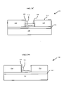
- a first conductor 12 is formed on a substrate 10 .
- an insulator 14 is formed on the first conductor 12 , and a via 18 is formed in the insulator 14 .
- a metallic material 16 such as silver is deposited on the insulator 14 and in the via 18 , after which a polishing step removes the metallic material 16 from the surface of the insulator 14 .
- a chalcogenide glass 22 is deposited over the metallic material 16 , followed by a metal-containing layer 24 and a second conductor 26 .
- a second polishing step removes the chalcogenide glass 22 , metal-containing layer 24 and second conductor 26 everywhere but within the via 18 .
- the first polishing step sometimes pulls the metallic material 16 out of the via 18 leaving no metal in the via 18 as shown in FIG. 1B .
- an undesired build up of slurry residual in the via 18 from the first polishing step has also been observed.
- the invention provides a method for forming a metal layer in a via that includes forming a metallic material on a surface of an insulator and within and over a bottom of the via, forming a hard mask over the metallic material in the via, removing the metallic material from the surface of the insulator, and removing the hard mask from the via.
- the invention also provides a method for making a programmable conductor random access memory.
- the method includes forming a first conductor on the substrate, forming an insulator on the substrate, forming a via in the insulator extending to the first conductor, forming a metallic material on a surface of the insulator and in the via in contact with the first conductor, forming a hard mask over said metallic material within the via, removing the metallic material from the surface of the insulator, removing the hard mask, forming a chalcogenide material in the via in contact with the metallic material, forming a metal-containing material in the via in contact with the chalcogenide material, and forming a second conductor on the surface of the insulator and in contact with the metal-containing material.
- the invention also provides a programmable conductor random access intermediate structure that includes a substrate, a first conductor formed on said substrate, an insulator formed on said first conductor, at least one via formed within said insulator and extending to said first conductor, a metallic material formed in said at least one via, and a hard mask formed on said metallic material within said at least one via.
- FIG. 1A is a schematic view of a PCRAM cell being formed in accordance with a conventional process.
- FIG. 1B is a view of the PCRAM cell of FIG. 1A with the metallic material removed from the via.
- FIG. 1C is a schematic view of the completed PCRAM cell of FIG. 1A .
- FIGS. 2A–2D are schematic views of the formation of a PCRAM cell in accordance with an embodiment of the invention.
- FIG. 3 illustrates a method for forming a PCRAM cell in accordance with an embodiment of the invention.
- FIG. 4 is a schematic view of a PCRAM cell formed by a method in accordance with an embodiment of the invention.
- PCRAM programmable conductor random access memory
- a PCRAM intermediate structure 100 is formed by, for example, depositing a first conductor 112 on a substrate 110 .
- the first conductor 112 may be formed of any suitable conducting material, such as, for example, tungsten, nickel, tantalum, titanium, titanium nitride, aluminum, platinum, and silver, among many others.
- the substrate 110 can be formed of any suitable material, such as, for example, semiconductor materials or insulating materials such as silicon or plastic.
- An insulator 114 is then formed on the first conductor 112 by, for example, deposition.
- the insulator 114 may be formed of any suitable insulating material, such as silicon nitride.
- a via 118 is then formed in the insulator 114 through any suitable process, such as, for example, patterning a masking material on a surface 115 of the insulator 114 and etching to remove unmasked portions of the insulator 114 .
- a conductive material such as a metallic film 116
- the metallic film 116 is formed through a deposition process, and most preferably through a plasma vapor sputter deposition of the metallic material.
- the metallic film 116 resides in a portion of the via 118 in contact with the first conductor 112 and does not adhere to the sides of the via 118 .
- the lack of adherence of the metallic film 116 on the sides of the via 118 is due to poor step coverage of the plasma vapor deposited metal.
- the metallic film 116 is a film of silver which is formed through a plasma vapor sputter deposition of silver.
- a flowable oxide 120 is deposited in the via 118 over the silver film 116 .
- the flowable oxide 120 has high mobility and it behaves like a liquid on a surface.
- the presence of the via 118 on the surface 115 of the insulator 114 allows the flowable oxide 120 to flow into the via 118 before distributing on the surface 115 ( FIG. 3 ).
- the flowable oxide 120 is deposited through a chemical vapor deposition using trimethylsilane and ozone as precursors.
- the highly mobile flowable oxide 120 flows to fill the portion of the via 118 directly above the silver film 116 , does not adhere to the sides of the via 118 , and does not remain lodged at the open end of the via 118 .
- the flowable oxide 120 is preferably silicon oxide, or alternatively, may be formed of a spin-on material having high mobility and being suitable to protect the metallic film 116 .
- the flow step 210 is performed at a relatively low temperature, specifically in the range of about 50° C. to about 90° C.
- a low temperature process is advantageous because a phase transition may occur at higher temperatures and silver from the silver film 116 may diffuse into surrounding material in the PCRAM intermediate structure at higher temperatures. Even at such low temperatures, the surface tension of the flowable oxide 120 is sufficient to drive the flowable oxide 120 to cover the silver film 116 .
- the flowable oxide 120 forms a hard mask that serves to protect the silver film 116 positioned beneath the flowable oxide 120 .
- the silver film 116 is removed from the surface 115 of the insulator 114 by a suitable process, such as, for example, dry sputter etching.
- a suitable process such as, for example, dry sputter etching.
- dry sputter etching the silver film 116 may be completely removed from the surface 115 .
- a portion of the flowable oxide 120 within the via 118 may also be removed through the dry sputter etching.
- a 1 mA/cm 2 sputter of argon corresponds to a sputter rate of 1833 A/s for the silver film 116 and only 400 A/s for the flowable oxide 120 .
- the flowable oxide 120 serves as a sufficient barrier against the deleterious effects of the dry sputter etching on the silver film 116 covered by the flowable oxide 120 within the via 118 .
- the remaining oxide material 120 is selectively removed.
- a suitable removal process is used, such as, for example, providing a hydrogen fluoride solution that etches silicon oxide (flowable oxide 120 ) at a much faster rate than either silicon nitride (insulator 114 ) or metal (metallic film 116 ).
- a via 118 is formed with a metallic film 116 contacting a conductor 112 within the via 118 .
- a glass material 122 is recessed in the via 118 through either a dry or wet etch.
- One exemplary wet etch incorporates NH 4 OH, while one exemplary dry etch incorporates a fluorine based chemistry, though any dry etch capable of removing oxides would be suitable.
- the glass material 122 may be a chalcogenide glass.
- One preferred chalcogenide glass is germanium-selenide glass with a Ge x Se 100-x stoichiometry between about Ge 20 SC 80 to about Ge 43 Se 57 .
- a metal-containing material layer 124 is formed in the via 118 over the glass material 122 .
- the metal-containing material layer 124 is then planarized to remove any of the layer from the surface 115 of the insulator.
- the metal-containing material 124 is preferably silver-selenide.
- a second conductor 126 is formed over the surface 115 of the insulator 114 and over the metal-containing layer 124 .
Abstract
Description
Claims (23)
Priority Applications (3)
| Application Number | Priority Date | Filing Date | Title |
|---|---|---|---|
| US10/388,264 US7022579B2 (en) | 2003-03-14 | 2003-03-14 | Method for filling via with metal |
| US10/758,102 US7126179B2 (en) | 2003-03-14 | 2004-01-16 | Memory cell intermediate structure |
| US11/516,730 US7410863B2 (en) | 2003-03-14 | 2006-09-07 | Methods of forming and using memory cell structures |
Applications Claiming Priority (2)
| Application Number | Priority Date | Filing Date | Title |
|---|---|---|---|
| US10/388,264 US7022579B2 (en) | 2003-03-14 | 2003-03-14 | Method for filling via with metal |
| US10/758,102 US7126179B2 (en) | 2003-03-14 | 2004-01-16 | Memory cell intermediate structure |
Related Child Applications (1)
| Application Number | Title | Priority Date | Filing Date |
|---|---|---|---|
| US10/758,102 Division US7126179B2 (en) | 2003-03-14 | 2004-01-16 | Memory cell intermediate structure |
Publications (2)
| Publication Number | Publication Date |
|---|---|
| US20040180533A1 US20040180533A1 (en) | 2004-09-16 |
| US7022579B2 true US7022579B2 (en) | 2006-04-04 |
Family
ID=46299062
Family Applications (3)
| Application Number | Title | Priority Date | Filing Date |
|---|---|---|---|
| US10/388,264 Expired - Lifetime US7022579B2 (en) | 2003-03-14 | 2003-03-14 | Method for filling via with metal |
| US10/758,102 Expired - Lifetime US7126179B2 (en) | 2003-03-14 | 2004-01-16 | Memory cell intermediate structure |
| US11/516,730 Expired - Lifetime US7410863B2 (en) | 2003-03-14 | 2006-09-07 | Methods of forming and using memory cell structures |
Family Applications After (2)
| Application Number | Title | Priority Date | Filing Date |
|---|---|---|---|
| US10/758,102 Expired - Lifetime US7126179B2 (en) | 2003-03-14 | 2004-01-16 | Memory cell intermediate structure |
| US11/516,730 Expired - Lifetime US7410863B2 (en) | 2003-03-14 | 2006-09-07 | Methods of forming and using memory cell structures |
Country Status (1)
| Country | Link |
|---|---|
| US (3) | US7022579B2 (en) |
Cited By (2)
| Publication number | Priority date | Publication date | Assignee | Title |
|---|---|---|---|---|
| US20050274942A1 (en) * | 2002-06-07 | 2005-12-15 | Kozicki Michael N | Nanoscale programmable structures and methods of forming and using same |
| US20080057691A1 (en) * | 2006-08-29 | 2008-03-06 | Dando Ross S | Methods and systems for selectively filling apertures in a substrate to form conductive vias with a liquid using a vacuum |
Families Citing this family (7)
| Publication number | Priority date | Publication date | Assignee | Title |
|---|---|---|---|---|
| KR100881055B1 (en) * | 2007-06-20 | 2009-01-30 | 삼성전자주식회사 | Phase-change memory unit, method of forming the phase-change memory unit, phase-change memory device having the phase-change memory unit and method of manufacturing the phase-change memory device |
| US7825479B2 (en) * | 2008-08-06 | 2010-11-02 | International Business Machines Corporation | Electrical antifuse having a multi-thickness dielectric layer |
| JP2011233835A (en) * | 2010-04-30 | 2011-11-17 | Toshiba Corp | Semiconductor memory and method of manufacturing the same |
| US9391016B2 (en) | 2014-04-10 | 2016-07-12 | Taiwan Semiconductor Manufacturing Co., Ltd. | MIM capacitor structure |
| US9219110B2 (en) | 2014-04-10 | 2015-12-22 | Taiwan Semiconductor Manufacturing Co., Ltd. | MIM capacitor structure |
| US9368392B2 (en) | 2014-04-10 | 2016-06-14 | Taiwan Semiconductor Manufacturing Co., Ltd. | MIM capacitor structure |
| US9425061B2 (en) * | 2014-05-29 | 2016-08-23 | Taiwan Semiconductor Manufacturing Co., Ltd. | Buffer cap layer to improve MIM structure performance |
Citations (93)
| Publication number | Priority date | Publication date | Assignee | Title |
|---|---|---|---|---|
| US3271591A (en) | 1963-09-20 | 1966-09-06 | Energy Conversion Devices Inc | Symmetrical current controlling device |
| US3622319A (en) | 1966-10-20 | 1971-11-23 | Western Electric Co | Nonreflecting photomasks and methods of making same |
| US3743847A (en) | 1971-06-01 | 1973-07-03 | Motorola Inc | Amorphous silicon film as a uv filter |
| US3961314A (en) | 1974-03-05 | 1976-06-01 | Energy Conversion Devices, Inc. | Structure and method for producing an image |
| US3966317A (en) | 1974-04-08 | 1976-06-29 | Energy Conversion Devices, Inc. | Dry process production of archival microform records from hard copy |
| US3983542A (en) | 1970-08-13 | 1976-09-28 | Energy Conversion Devices, Inc. | Method and apparatus for recording information |
| US4177474A (en) | 1977-05-18 | 1979-12-04 | Energy Conversion Devices, Inc. | High temperature amorphous semiconductor member and method of making the same |
| US4267261A (en) | 1971-07-15 | 1981-05-12 | Energy Conversion Devices, Inc. | Method for full format imaging |
| US4269935A (en) | 1979-07-13 | 1981-05-26 | Ionomet Company, Inc. | Process of doping silver image in chalcogenide layer |
| US4312938A (en) | 1979-07-06 | 1982-01-26 | Drexler Technology Corporation | Method for making a broadband reflective laser recording and data storage medium with absorptive underlayer |
| US4316946A (en) | 1979-12-03 | 1982-02-23 | Ionomet Company, Inc. | Surface sensitized chalcogenide product and process for making and using the same |
| US4320191A (en) | 1978-11-07 | 1982-03-16 | Nippon Telegraph & Telephone Public Corporation | Pattern-forming process |
| US4405710A (en) | 1981-06-22 | 1983-09-20 | Cornell Research Foundation, Inc. | Ion beam exposure of (g-Gex -Se1-x) inorganic resists |
| US4419421A (en) | 1979-01-15 | 1983-12-06 | Max-Planck-Gesellschaft Zur Forderung Der Wissenschaften E.V. | Ion conductor material |
| US4499557A (en) | 1980-10-28 | 1985-02-12 | Energy Conversion Devices, Inc. | Programmable cell for use in programmable electronic arrays |
| US4597162A (en) | 1983-01-18 | 1986-07-01 | Energy Conversion Devices, Inc. | Method for making, parallel preprogramming or field programming of electronic matrix arrays |
| US4608296A (en) | 1983-12-06 | 1986-08-26 | Energy Conversion Devices, Inc. | Superconducting films and devices exhibiting AC to DC conversion |
| US4637895A (en) | 1985-04-01 | 1987-01-20 | Energy Conversion Devices, Inc. | Gas mixtures for the vapor deposition of semiconductor material |
| US4646266A (en) | 1984-09-28 | 1987-02-24 | Energy Conversion Devices, Inc. | Programmable semiconductor structures and methods for using the same |
| US4664939A (en) | 1985-04-01 | 1987-05-12 | Energy Conversion Devices, Inc. | Vertical semiconductor processor |
| US4668968A (en) | 1984-05-14 | 1987-05-26 | Energy Conversion Devices, Inc. | Integrated circuit compatible thin film field effect transistor and method of making same |
| US4670763A (en) | 1984-05-14 | 1987-06-02 | Energy Conversion Devices, Inc. | Thin film field effect transistor |
| US4671618A (en) | 1986-05-22 | 1987-06-09 | Wu Bao Gang | Liquid crystalline-plastic material having submillisecond switch times and extended memory |
| US4673957A (en) | 1984-05-14 | 1987-06-16 | Energy Conversion Devices, Inc. | Integrated circuit compatible thin film field effect transistor and method of making same |
| US4678679A (en) | 1984-06-25 | 1987-07-07 | Energy Conversion Devices, Inc. | Continuous deposition of activated process gases |
| US4710899A (en) | 1985-06-10 | 1987-12-01 | Energy Conversion Devices, Inc. | Data storage medium incorporating a transition metal for increased switching speed |
| US4728406A (en) | 1986-08-18 | 1988-03-01 | Energy Conversion Devices, Inc. | Method for plasma - coating a semiconductor body |
| US4737379A (en) | 1982-09-24 | 1988-04-12 | Energy Conversion Devices, Inc. | Plasma deposited coatings, and low temperature plasma method of making same |
| US4766471A (en) | 1986-01-23 | 1988-08-23 | Energy Conversion Devices, Inc. | Thin film electro-optical devices |
| US4769338A (en) | 1984-05-14 | 1988-09-06 | Energy Conversion Devices, Inc. | Thin film field effect transistor and method of making same |
| US4775425A (en) | 1987-07-27 | 1988-10-04 | Energy Conversion Devices, Inc. | P and n-type microcrystalline semiconductor alloy material including band gap widening elements, devices utilizing same |
| US4788594A (en) | 1986-10-15 | 1988-11-29 | Energy Conversion Devices, Inc. | Solid state electronic camera including thin film matrix of photosensors |
| US4795657A (en) | 1984-04-13 | 1989-01-03 | Energy Conversion Devices, Inc. | Method of fabricating a programmable array |
| US4800526A (en) | 1987-05-08 | 1989-01-24 | Gaf Corporation | Memory element for information storage and retrieval system and associated process |
| US4809044A (en) | 1986-08-22 | 1989-02-28 | Energy Conversion Devices, Inc. | Thin film overvoltage protection devices |
| US4818717A (en) | 1986-06-27 | 1989-04-04 | Energy Conversion Devices, Inc. | Method for making electronic matrix arrays |
| US4843443A (en) | 1984-05-14 | 1989-06-27 | Energy Conversion Devices, Inc. | Thin film field effect transistor and method of making same |
| US4845533A (en) | 1986-08-22 | 1989-07-04 | Energy Conversion Devices, Inc. | Thin film electrical devices with amorphous carbon electrodes and method of making same |
| US4847674A (en) | 1987-03-10 | 1989-07-11 | Advanced Micro Devices, Inc. | High speed interconnect system with refractory non-dogbone contacts and an active electromigration suppression mechanism |
| US4853785A (en) | 1986-10-15 | 1989-08-01 | Energy Conversion Devices, Inc. | Electronic camera including electronic signal storage cartridge |
| US4891330A (en) | 1987-07-27 | 1990-01-02 | Energy Conversion Devices, Inc. | Method of fabricating n-type and p-type microcrystalline semiconductor alloy material including band gap widening elements |
| US5128099A (en) | 1991-02-15 | 1992-07-07 | Energy Conversion Devices, Inc. | Congruent state changeable optical memory material and device |
| US5159661A (en) | 1990-10-05 | 1992-10-27 | Energy Conversion Devices, Inc. | Vertically interconnected parallel distributed processor |
| US5166758A (en) | 1991-01-18 | 1992-11-24 | Energy Conversion Devices, Inc. | Electrically erasable phase change memory |
| US5177567A (en) | 1991-07-19 | 1993-01-05 | Energy Conversion Devices, Inc. | Thin-film structure for chalcogenide electrical switching devices and process therefor |
| US5219788A (en) | 1991-02-25 | 1993-06-15 | Ibm Corporation | Bilayer metallization cap for photolithography |
| US5238862A (en) | 1992-03-18 | 1993-08-24 | Micron Technology, Inc. | Method of forming a stacked capacitor with striated electrode |
| US5272359A (en) | 1988-04-07 | 1993-12-21 | California Institute Of Technology | Reversible non-volatile switch based on a TCNQ charge transfer complex |
| US5296716A (en) | 1991-01-18 | 1994-03-22 | Energy Conversion Devices, Inc. | Electrically erasable, directly overwritable, multibit single cell memory elements and arrays fabricated therefrom |
| US5314772A (en) | 1990-10-09 | 1994-05-24 | Arizona Board Of Regents | High resolution, multi-layer resist for microlithography and method therefor |
| US5315131A (en) | 1990-11-22 | 1994-05-24 | Matsushita Electric Industrial Co., Ltd. | Electrically reprogrammable nonvolatile memory device |
| US5335219A (en) | 1991-01-18 | 1994-08-02 | Ovshinsky Stanford R | Homogeneous composition of microcrystalline semiconductor material, semiconductor devices and directly overwritable memory elements fabricated therefrom, and arrays fabricated from the memory elements |
| US5341328A (en) | 1991-01-18 | 1994-08-23 | Energy Conversion Devices, Inc. | Electrically erasable memory elements having reduced switching current requirements and increased write/erase cycle life |
| US5350484A (en) | 1992-09-08 | 1994-09-27 | Intel Corporation | Method for the anisotropic etching of metal films in the fabrication of interconnects |
| US5359205A (en) | 1991-11-07 | 1994-10-25 | Energy Conversion Devices, Inc. | Electrically erasable memory elements characterized by reduced current and improved thermal stability |
| US5360981A (en) | 1989-05-11 | 1994-11-01 | British Telecommunications Public Limited Company | Amorphous silicon memory |
| US5406509A (en) | 1991-01-18 | 1995-04-11 | Energy Conversion Devices, Inc. | Electrically erasable, directly overwritable, multibit single cell memory elements and arrays fabricated therefrom |
| US5414271A (en) | 1991-01-18 | 1995-05-09 | Energy Conversion Devices, Inc. | Electrically erasable memory elements having improved set resistance stability |
| US5500532A (en) | 1994-08-18 | 1996-03-19 | Arizona Board Of Regents | Personal electronic dosimeter |
| US5512328A (en) | 1992-08-07 | 1996-04-30 | Hitachi, Ltd. | Method for forming a pattern and forming a thin film used in pattern formation |
| US5512773A (en) | 1993-12-23 | 1996-04-30 | U.S. Philips Corporation | Switching element with memory provided with Schottky tunnelling barrier |
| US5534712A (en) | 1991-01-18 | 1996-07-09 | Energy Conversion Devices, Inc. | Electrically erasable memory elements characterized by reduced current and improved thermal stability |
| US5534711A (en) | 1991-01-18 | 1996-07-09 | Energy Conversion Devices, Inc. | Electrically erasable, directly overwritable, multibit single cell memory elements and arrays fabricated therefrom |
| US5536947A (en) | 1991-01-18 | 1996-07-16 | Energy Conversion Devices, Inc. | Electrically erasable, directly overwritable, multibit single cell memory element and arrays fabricated therefrom |
| US5543737A (en) | 1995-02-10 | 1996-08-06 | Energy Conversion Devices, Inc. | Logical operation circuit employing two-terminal chalcogenide switches |
| US5591501A (en) | 1995-12-20 | 1997-01-07 | Energy Conversion Devices, Inc. | Optical recording medium having a plurality of discrete phase change data recording points |
| US5596522A (en) | 1991-01-18 | 1997-01-21 | Energy Conversion Devices, Inc. | Homogeneous compositions of microcrystalline semiconductor material, semiconductor devices and directly overwritable memory elements fabricated therefrom, and arrays fabricated from the memory elements |
| US5687112A (en) | 1996-04-19 | 1997-11-11 | Energy Conversion Devices, Inc. | Multibit single cell memory element having tapered contact |
| US5694054A (en) | 1995-11-28 | 1997-12-02 | Energy Conversion Devices, Inc. | Integrated drivers for flat panel displays employing chalcogenide logic elements |
| US5714768A (en) | 1995-10-24 | 1998-02-03 | Energy Conversion Devices, Inc. | Second-layer phase change memory array on top of a logic device |
| US5726083A (en) | 1994-11-29 | 1998-03-10 | Nec Corporation | Process of fabricating dynamic random access memory device having storage capacitor low in contact resistance and small in leakage current through tantalum oxide film |
| US5751012A (en) | 1995-06-07 | 1998-05-12 | Micron Technology, Inc. | Polysilicon pillar diode for use in a non-volatile memory cell |
| US5761115A (en) | 1996-05-30 | 1998-06-02 | Axon Technologies Corporation | Programmable metallization cell structure and method of making same |
| US5789277A (en) | 1996-07-22 | 1998-08-04 | Micron Technology, Inc. | Method of making chalogenide memory device |
| US5814527A (en) | 1996-07-22 | 1998-09-29 | Micron Technology, Inc. | Method of making small pores defined by a disposable internal spacer for use in chalcogenide memories |
| US5818749A (en) | 1993-08-20 | 1998-10-06 | Micron Technology, Inc. | Integrated circuit memory device |
| US5825046A (en) | 1996-10-28 | 1998-10-20 | Energy Conversion Devices, Inc. | Composite memory material comprising a mixture of phase-change memory material and dielectric material |
| US5841150A (en) | 1995-06-07 | 1998-11-24 | Micron Technology, Inc. | Stack/trench diode for use with a muti-state material in a non-volatile memory cell |
| US5846889A (en) | 1997-03-14 | 1998-12-08 | The United States Of America As Represented By The Secretary Of The Navy | Infrared transparent selenide glasses |
| US5851882A (en) | 1996-05-06 | 1998-12-22 | Micron Technology, Inc. | ZPROM manufacture and design and methods for forming thin structures using spacers as an etching mask |
| US5869843A (en) | 1995-06-07 | 1999-02-09 | Micron Technology, Inc. | Memory array having a multi-state element and method for forming such array or cells thereof |
| US5912839A (en) | 1998-06-23 | 1999-06-15 | Energy Conversion Devices, Inc. | Universal memory element and method of programming same |
| US5920788A (en) | 1995-06-07 | 1999-07-06 | Micron Technology, Inc. | Chalcogenide memory cell with a plurality of chalcogenide electrodes |
| US5933365A (en) | 1997-06-19 | 1999-08-03 | Energy Conversion Devices, Inc. | Memory element with energy control mechanism |
| US5998066A (en) | 1997-05-16 | 1999-12-07 | Aerial Imaging Corporation | Gray scale mask and depth pattern transfer technique using inorganic chalcogenide glass |
| US6011757A (en) | 1998-01-27 | 2000-01-04 | Ovshinsky; Stanford R. | Optical recording media having increased erasability |
| US6031287A (en) | 1997-06-18 | 2000-02-29 | Micron Technology, Inc. | Contact structure and memory element incorporating the same |
| US6072716A (en) | 1999-04-14 | 2000-06-06 | Massachusetts Institute Of Technology | Memory structures and methods of making same |
| US6087674A (en) | 1996-10-28 | 2000-07-11 | Energy Conversion Devices, Inc. | Memory element with memory material comprising phase-change material and dielectric material |
| US6117720A (en) | 1995-06-07 | 2000-09-12 | Micron Technology, Inc. | Method of making an integrated circuit electrode having a reduced contact area |
| US6141241A (en) | 1998-06-23 | 2000-10-31 | Energy Conversion Devices, Inc. | Universal memory element with systems employing same and apparatus and method for reading, writing and programming same |
| US6143604A (en) | 1999-06-04 | 2000-11-07 | Taiwan Semiconductor Manufacturing Company | Method for fabricating small-size two-step contacts for word-line strapping on dynamic random access memory (DRAM) |
| US6376370B1 (en) * | 2000-01-18 | 2002-04-23 | Micron Technology, Inc. | Process for providing seed layers for using aluminum, copper, gold and silver metallurgy process for providing seed layers for using aluminum, copper, gold and silver metallurgy |
Family Cites Families (73)
| Publication number | Priority date | Publication date | Assignee | Title |
|---|---|---|---|---|
| US667348A (en) * | 1900-06-27 | 1901-02-05 | John B Houston | Tire for vehicle-wheels. |
| JP2804206B2 (en) * | 1992-09-22 | 1998-09-24 | 三菱電機株式会社 | Laser processing head |
| US5879955A (en) * | 1995-06-07 | 1999-03-09 | Micron Technology, Inc. | Method for fabricating an array of ultra-small pores for chalcogenide memory cells |
| US6653733B1 (en) * | 1996-02-23 | 2003-11-25 | Micron Technology, Inc. | Conductors in semiconductor devices |
| US5852870A (en) | 1996-04-24 | 1998-12-29 | Amkor Technology, Inc. | Method of making grid array assembly |
| US5998244A (en) * | 1996-08-22 | 1999-12-07 | Micron Technology, Inc. | Memory cell incorporating a chalcogenide element and method of making same |
| US6051511A (en) | 1997-07-31 | 2000-04-18 | Micron Technology, Inc. | Method and apparatus for reducing isolation stress in integrated circuits |
| WO1999028914A2 (en) | 1997-12-04 | 1999-06-10 | Axon Technologies Corporation | Programmable sub-surface aggregating metallization structure and method of making same |
| US5883006A (en) * | 1997-12-12 | 1999-03-16 | Kabushiki Kaisha Toshiba | Method for making a semiconductor device using a flowable oxide film |
| US6297170B1 (en) | 1998-06-23 | 2001-10-02 | Vlsi Technology, Inc. | Sacrificial multilayer anti-reflective coating for mos gate formation |
| US6388324B2 (en) * | 1998-08-31 | 2002-05-14 | Arizona Board Of Regents | Self-repairing interconnections for electrical circuits |
| US6469364B1 (en) | 1998-08-31 | 2002-10-22 | Arizona Board Of Regents | Programmable interconnection system for electrical circuits |
| US6985378B2 (en) | 1998-12-04 | 2006-01-10 | Axon Technologies Corporation | Programmable microelectronic device, structure, and system and method of forming the same |
| US6487106B1 (en) * | 1999-01-12 | 2002-11-26 | Arizona Board Of Regents | Programmable microelectronic devices and method of forming and programming same |
| US6635914B2 (en) | 2000-09-08 | 2003-10-21 | Axon Technologies Corp. | Microelectronic programmable device and methods of forming and programming the same |
| US6825489B2 (en) * | 2001-04-06 | 2004-11-30 | Axon Technologies Corporation | Microelectronic device, structure, and system, including a memory structure having a variable programmable property and method of forming the same |
| US6177338B1 (en) * | 1999-02-08 | 2001-01-23 | Taiwan Semiconductor Manufacturing Company | Two step barrier process |
| US6350679B1 (en) * | 1999-08-03 | 2002-02-26 | Micron Technology, Inc. | Methods of providing an interlevel dielectric layer intermediate different elevation conductive metal layers in the fabrication of integrated circuitry |
| US20030107105A1 (en) | 1999-08-31 | 2003-06-12 | Kozicki Michael N. | Programmable chip-to-substrate interconnect structure and device and method of forming same |
| JP2001111026A (en) * | 1999-10-07 | 2001-04-20 | Fuji Film Microdevices Co Ltd | Solid state image sensor |
| US6423628B1 (en) | 1999-10-22 | 2002-07-23 | Lsi Logic Corporation | Method of forming integrated circuit structure having low dielectric constant material and having silicon oxynitride caps over closely spaced apart metal lines |
| US6865117B2 (en) * | 2000-02-11 | 2005-03-08 | Axon Technologies Corporation | Programming circuit for a programmable microelectronic device, system including the circuit, and method of forming the same |
| US6914802B2 (en) * | 2000-02-11 | 2005-07-05 | Axon Technologies Corporation | Microelectronic photonic structure and device and method of forming the same |
| US6440837B1 (en) | 2000-07-14 | 2002-08-27 | Micron Technology, Inc. | Method of forming a contact structure in a semiconductor device |
| US6563156B2 (en) | 2001-03-15 | 2003-05-13 | Micron Technology, Inc. | Memory elements and methods for making same |
| US6563164B2 (en) * | 2000-09-29 | 2003-05-13 | Ovonyx, Inc. | Compositionally modified resistive electrode |
| US6339544B1 (en) * | 2000-09-29 | 2002-01-15 | Intel Corporation | Method to enhance performance of thermal resistor device |
| US6567293B1 (en) * | 2000-09-29 | 2003-05-20 | Ovonyx, Inc. | Single level metal memory cell using chalcogenide cladding |
| US6555860B2 (en) * | 2000-09-29 | 2003-04-29 | Intel Corporation | Compositionally modified resistive electrode |
| US6653193B2 (en) * | 2000-12-08 | 2003-11-25 | Micron Technology, Inc. | Resistance variable device |
| US6696355B2 (en) * | 2000-12-14 | 2004-02-24 | Ovonyx, Inc. | Method to selectively increase the top resistance of the lower programming electrode in a phase-change memory |
| US6569705B2 (en) * | 2000-12-21 | 2003-05-27 | Intel Corporation | Metal structure for a phase-change memory device |
| US6534781B2 (en) * | 2000-12-26 | 2003-03-18 | Ovonyx, Inc. | Phase-change memory bipolar array utilizing a single shallow trench isolation for creating an individual active area region for two memory array elements and one bipolar base contact |
| US6531373B2 (en) * | 2000-12-27 | 2003-03-11 | Ovonyx, Inc. | Method of forming a phase-change memory cell using silicon on insulator low electrode in charcogenide elements |
| US6687427B2 (en) * | 2000-12-29 | 2004-02-03 | Intel Corporation | Optic switch |
| US6638820B2 (en) | 2001-02-08 | 2003-10-28 | Micron Technology, Inc. | Method of forming chalcogenide comprising devices, method of precluding diffusion of a metal into adjacent chalcogenide material, and chalcogenide comprising devices |
| US6727192B2 (en) | 2001-03-01 | 2004-04-27 | Micron Technology, Inc. | Methods of metal doping a chalcogenide material |
| US6348365B1 (en) | 2001-03-02 | 2002-02-19 | Micron Technology, Inc. | PCRAM cell manufacturing |
| US6818481B2 (en) | 2001-03-07 | 2004-11-16 | Micron Technology, Inc. | Method to manufacture a buried electrode PCRAM cell |
| US6734455B2 (en) | 2001-03-15 | 2004-05-11 | Micron Technology, Inc. | Agglomeration elimination for metal sputter deposition of chalcogenides |
| US6473332B1 (en) | 2001-04-04 | 2002-10-29 | The University Of Houston System | Electrically variable multi-state resistance computing |
| CN100403450C (en) | 2001-05-07 | 2008-07-16 | 先进微装置公司 | Memory device with self-assembled polymer film and method of making the same |
| US7102150B2 (en) | 2001-05-11 | 2006-09-05 | Harshfield Steven T | PCRAM memory cell and method of making same |
| US6570784B2 (en) * | 2001-06-29 | 2003-05-27 | Ovonyx, Inc. | Programming a phase-change material memory |
| US6511867B2 (en) * | 2001-06-30 | 2003-01-28 | Ovonyx, Inc. | Utilizing atomic layer deposition for programmable device |
| US6511862B2 (en) * | 2001-06-30 | 2003-01-28 | Ovonyx, Inc. | Modified contact for programmable devices |
| US6673700B2 (en) * | 2001-06-30 | 2004-01-06 | Ovonyx, Inc. | Reduced area intersection between electrode and programming element |
| US6951805B2 (en) * | 2001-08-01 | 2005-10-04 | Micron Technology, Inc. | Method of forming integrated circuitry, method of forming memory circuitry, and method of forming random access memory circuitry |
| US6590807B2 (en) * | 2001-08-02 | 2003-07-08 | Intel Corporation | Method for reading a structural phase-change memory |
| US6737312B2 (en) * | 2001-08-27 | 2004-05-18 | Micron Technology, Inc. | Method of fabricating dual PCRAM cells sharing a common electrode |
| US6784018B2 (en) | 2001-08-29 | 2004-08-31 | Micron Technology, Inc. | Method of forming chalcogenide comprising devices and method of forming a programmable memory cell of memory circuitry |
| US6955940B2 (en) * | 2001-08-29 | 2005-10-18 | Micron Technology, Inc. | Method of forming chalcogenide comprising devices |
| US6881623B2 (en) * | 2001-08-29 | 2005-04-19 | Micron Technology, Inc. | Method of forming chalcogenide comprising devices, method of forming a programmable memory cell of memory circuitry, and a chalcogenide comprising device |
| US6646902B2 (en) * | 2001-08-30 | 2003-11-11 | Micron Technology, Inc. | Method of retaining memory state in a programmable conductor RAM |
| US20030047765A1 (en) * | 2001-08-30 | 2003-03-13 | Campbell Kristy A. | Stoichiometry for chalcogenide glasses useful for memory devices and method of formation |
| US6709958B2 (en) * | 2001-08-30 | 2004-03-23 | Micron Technology, Inc. | Integrated circuit device and fabrication using metal-doped chalcogenide materials |
| US6507061B1 (en) * | 2001-08-31 | 2003-01-14 | Intel Corporation | Multiple layer phase-change memory |
| EP2112659A1 (en) * | 2001-09-01 | 2009-10-28 | Energy Convertion Devices, Inc. | Increased data storage in optical data storage and retrieval systems using blue lasers and/or plasmon lenses |
| US6545287B2 (en) * | 2001-09-07 | 2003-04-08 | Intel Corporation | Using selective deposition to form phase-change memory cells |
| US6690026B2 (en) * | 2001-09-28 | 2004-02-10 | Intel Corporation | Method of fabricating a three-dimensional array of active media |
| US6566700B2 (en) * | 2001-10-11 | 2003-05-20 | Ovonyx, Inc. | Carbon-containing interfacial layer for phase-change memory |
| US6545907B1 (en) * | 2001-10-30 | 2003-04-08 | Ovonyx, Inc. | Technique and apparatus for performing write operations to a phase change material memory device |
| US6815818B2 (en) * | 2001-11-19 | 2004-11-09 | Micron Technology, Inc. | Electrode structure for use in an integrated circuit |
| US6791859B2 (en) * | 2001-11-20 | 2004-09-14 | Micron Technology, Inc. | Complementary bit PCRAM sense amplifier and method of operation |
| US6873538B2 (en) | 2001-12-20 | 2005-03-29 | Micron Technology, Inc. | Programmable conductor random access memory and a method for writing thereto |
| US6512241B1 (en) * | 2001-12-31 | 2003-01-28 | Intel Corporation | Phase change material memory device |
| US6909656B2 (en) | 2002-01-04 | 2005-06-21 | Micron Technology, Inc. | PCRAM rewrite prevention |
| US20030143782A1 (en) * | 2002-01-31 | 2003-07-31 | Gilton Terry L. | Methods of forming germanium selenide comprising devices and methods of forming silver selenide comprising structures |
| US6867064B2 (en) * | 2002-02-15 | 2005-03-15 | Micron Technology, Inc. | Method to alter chalcogenide glass for improved switching characteristics |
| US6791885B2 (en) * | 2002-02-19 | 2004-09-14 | Micron Technology, Inc. | Programmable conductor random access memory and method for sensing same |
| US7151273B2 (en) * | 2002-02-20 | 2006-12-19 | Micron Technology, Inc. | Silver-selenide/chalcogenide glass stack for resistance variable memory |
| US6671710B2 (en) * | 2002-05-10 | 2003-12-30 | Energy Conversion Devices, Inc. | Methods of computing with digital multistate phase change materials |
| US6918382B2 (en) * | 2002-08-26 | 2005-07-19 | Energy Conversion Devices, Inc. | Hydrogen powered scooter |
-
2003
- 2003-03-14 US US10/388,264 patent/US7022579B2/en not_active Expired - Lifetime
-
2004
- 2004-01-16 US US10/758,102 patent/US7126179B2/en not_active Expired - Lifetime
-
2006
- 2006-09-07 US US11/516,730 patent/US7410863B2/en not_active Expired - Lifetime
Patent Citations (100)
| Publication number | Priority date | Publication date | Assignee | Title |
|---|---|---|---|---|
| US3271591A (en) | 1963-09-20 | 1966-09-06 | Energy Conversion Devices Inc | Symmetrical current controlling device |
| US3622319A (en) | 1966-10-20 | 1971-11-23 | Western Electric Co | Nonreflecting photomasks and methods of making same |
| US3983542A (en) | 1970-08-13 | 1976-09-28 | Energy Conversion Devices, Inc. | Method and apparatus for recording information |
| US3988720A (en) | 1970-08-13 | 1976-10-26 | Energy Conversion Devices, Inc. | Recording and retrieving information in an amorphous memory material using a catalytic material |
| US3743847A (en) | 1971-06-01 | 1973-07-03 | Motorola Inc | Amorphous silicon film as a uv filter |
| US4267261A (en) | 1971-07-15 | 1981-05-12 | Energy Conversion Devices, Inc. | Method for full format imaging |
| US3961314A (en) | 1974-03-05 | 1976-06-01 | Energy Conversion Devices, Inc. | Structure and method for producing an image |
| US3966317A (en) | 1974-04-08 | 1976-06-29 | Energy Conversion Devices, Inc. | Dry process production of archival microform records from hard copy |
| US4177474A (en) | 1977-05-18 | 1979-12-04 | Energy Conversion Devices, Inc. | High temperature amorphous semiconductor member and method of making the same |
| US4320191A (en) | 1978-11-07 | 1982-03-16 | Nippon Telegraph & Telephone Public Corporation | Pattern-forming process |
| US4419421A (en) | 1979-01-15 | 1983-12-06 | Max-Planck-Gesellschaft Zur Forderung Der Wissenschaften E.V. | Ion conductor material |
| US4312938A (en) | 1979-07-06 | 1982-01-26 | Drexler Technology Corporation | Method for making a broadband reflective laser recording and data storage medium with absorptive underlayer |
| US4269935A (en) | 1979-07-13 | 1981-05-26 | Ionomet Company, Inc. | Process of doping silver image in chalcogenide layer |
| US4316946A (en) | 1979-12-03 | 1982-02-23 | Ionomet Company, Inc. | Surface sensitized chalcogenide product and process for making and using the same |
| US4499557A (en) | 1980-10-28 | 1985-02-12 | Energy Conversion Devices, Inc. | Programmable cell for use in programmable electronic arrays |
| US4405710A (en) | 1981-06-22 | 1983-09-20 | Cornell Research Foundation, Inc. | Ion beam exposure of (g-Gex -Se1-x) inorganic resists |
| US4737379A (en) | 1982-09-24 | 1988-04-12 | Energy Conversion Devices, Inc. | Plasma deposited coatings, and low temperature plasma method of making same |
| US4597162A (en) | 1983-01-18 | 1986-07-01 | Energy Conversion Devices, Inc. | Method for making, parallel preprogramming or field programming of electronic matrix arrays |
| US4608296A (en) | 1983-12-06 | 1986-08-26 | Energy Conversion Devices, Inc. | Superconducting films and devices exhibiting AC to DC conversion |
| US4795657A (en) | 1984-04-13 | 1989-01-03 | Energy Conversion Devices, Inc. | Method of fabricating a programmable array |
| US4673957A (en) | 1984-05-14 | 1987-06-16 | Energy Conversion Devices, Inc. | Integrated circuit compatible thin film field effect transistor and method of making same |
| US4769338A (en) | 1984-05-14 | 1988-09-06 | Energy Conversion Devices, Inc. | Thin film field effect transistor and method of making same |
| US4670763A (en) | 1984-05-14 | 1987-06-02 | Energy Conversion Devices, Inc. | Thin film field effect transistor |
| US4843443A (en) | 1984-05-14 | 1989-06-27 | Energy Conversion Devices, Inc. | Thin film field effect transistor and method of making same |
| US4668968A (en) | 1984-05-14 | 1987-05-26 | Energy Conversion Devices, Inc. | Integrated circuit compatible thin film field effect transistor and method of making same |
| US4678679A (en) | 1984-06-25 | 1987-07-07 | Energy Conversion Devices, Inc. | Continuous deposition of activated process gases |
| US4646266A (en) | 1984-09-28 | 1987-02-24 | Energy Conversion Devices, Inc. | Programmable semiconductor structures and methods for using the same |
| US4637895A (en) | 1985-04-01 | 1987-01-20 | Energy Conversion Devices, Inc. | Gas mixtures for the vapor deposition of semiconductor material |
| US4696758A (en) | 1985-04-01 | 1987-09-29 | Energy Conversion Devices, Inc. | Gas mixtures for the vapor deposition of semiconductor material |
| US4698234A (en) | 1985-04-01 | 1987-10-06 | Energy Conversion Devices, Inc. | Vapor deposition of semiconductor material |
| US4664939A (en) | 1985-04-01 | 1987-05-12 | Energy Conversion Devices, Inc. | Vertical semiconductor processor |
| US4710899A (en) | 1985-06-10 | 1987-12-01 | Energy Conversion Devices, Inc. | Data storage medium incorporating a transition metal for increased switching speed |
| US4766471A (en) | 1986-01-23 | 1988-08-23 | Energy Conversion Devices, Inc. | Thin film electro-optical devices |
| US4671618A (en) | 1986-05-22 | 1987-06-09 | Wu Bao Gang | Liquid crystalline-plastic material having submillisecond switch times and extended memory |
| US4818717A (en) | 1986-06-27 | 1989-04-04 | Energy Conversion Devices, Inc. | Method for making electronic matrix arrays |
| US4728406A (en) | 1986-08-18 | 1988-03-01 | Energy Conversion Devices, Inc. | Method for plasma - coating a semiconductor body |
| US4809044A (en) | 1986-08-22 | 1989-02-28 | Energy Conversion Devices, Inc. | Thin film overvoltage protection devices |
| US4845533A (en) | 1986-08-22 | 1989-07-04 | Energy Conversion Devices, Inc. | Thin film electrical devices with amorphous carbon electrodes and method of making same |
| US4788594A (en) | 1986-10-15 | 1988-11-29 | Energy Conversion Devices, Inc. | Solid state electronic camera including thin film matrix of photosensors |
| US4853785A (en) | 1986-10-15 | 1989-08-01 | Energy Conversion Devices, Inc. | Electronic camera including electronic signal storage cartridge |
| US4847674A (en) | 1987-03-10 | 1989-07-11 | Advanced Micro Devices, Inc. | High speed interconnect system with refractory non-dogbone contacts and an active electromigration suppression mechanism |
| US4800526A (en) | 1987-05-08 | 1989-01-24 | Gaf Corporation | Memory element for information storage and retrieval system and associated process |
| US4891330A (en) | 1987-07-27 | 1990-01-02 | Energy Conversion Devices, Inc. | Method of fabricating n-type and p-type microcrystalline semiconductor alloy material including band gap widening elements |
| US4775425A (en) | 1987-07-27 | 1988-10-04 | Energy Conversion Devices, Inc. | P and n-type microcrystalline semiconductor alloy material including band gap widening elements, devices utilizing same |
| US5272359A (en) | 1988-04-07 | 1993-12-21 | California Institute Of Technology | Reversible non-volatile switch based on a TCNQ charge transfer complex |
| US5360981A (en) | 1989-05-11 | 1994-11-01 | British Telecommunications Public Limited Company | Amorphous silicon memory |
| US5159661A (en) | 1990-10-05 | 1992-10-27 | Energy Conversion Devices, Inc. | Vertically interconnected parallel distributed processor |
| US5314772A (en) | 1990-10-09 | 1994-05-24 | Arizona Board Of Regents | High resolution, multi-layer resist for microlithography and method therefor |
| US5315131A (en) | 1990-11-22 | 1994-05-24 | Matsushita Electric Industrial Co., Ltd. | Electrically reprogrammable nonvolatile memory device |
| US5296716A (en) | 1991-01-18 | 1994-03-22 | Energy Conversion Devices, Inc. | Electrically erasable, directly overwritable, multibit single cell memory elements and arrays fabricated therefrom |
| US5414271A (en) | 1991-01-18 | 1995-05-09 | Energy Conversion Devices, Inc. | Electrically erasable memory elements having improved set resistance stability |
| US5596522A (en) | 1991-01-18 | 1997-01-21 | Energy Conversion Devices, Inc. | Homogeneous compositions of microcrystalline semiconductor material, semiconductor devices and directly overwritable memory elements fabricated therefrom, and arrays fabricated from the memory elements |
| US5536947A (en) | 1991-01-18 | 1996-07-16 | Energy Conversion Devices, Inc. | Electrically erasable, directly overwritable, multibit single cell memory element and arrays fabricated therefrom |
| US5166758A (en) | 1991-01-18 | 1992-11-24 | Energy Conversion Devices, Inc. | Electrically erasable phase change memory |
| US5335219A (en) | 1991-01-18 | 1994-08-02 | Ovshinsky Stanford R | Homogeneous composition of microcrystalline semiconductor material, semiconductor devices and directly overwritable memory elements fabricated therefrom, and arrays fabricated from the memory elements |
| US5341328A (en) | 1991-01-18 | 1994-08-23 | Energy Conversion Devices, Inc. | Electrically erasable memory elements having reduced switching current requirements and increased write/erase cycle life |
| US5534711A (en) | 1991-01-18 | 1996-07-09 | Energy Conversion Devices, Inc. | Electrically erasable, directly overwritable, multibit single cell memory elements and arrays fabricated therefrom |
| US5534712A (en) | 1991-01-18 | 1996-07-09 | Energy Conversion Devices, Inc. | Electrically erasable memory elements characterized by reduced current and improved thermal stability |
| US5406509A (en) | 1991-01-18 | 1995-04-11 | Energy Conversion Devices, Inc. | Electrically erasable, directly overwritable, multibit single cell memory elements and arrays fabricated therefrom |
| US5128099A (en) | 1991-02-15 | 1992-07-07 | Energy Conversion Devices, Inc. | Congruent state changeable optical memory material and device |
| US5219788A (en) | 1991-02-25 | 1993-06-15 | Ibm Corporation | Bilayer metallization cap for photolithography |
| US5177567A (en) | 1991-07-19 | 1993-01-05 | Energy Conversion Devices, Inc. | Thin-film structure for chalcogenide electrical switching devices and process therefor |
| US5359205A (en) | 1991-11-07 | 1994-10-25 | Energy Conversion Devices, Inc. | Electrically erasable memory elements characterized by reduced current and improved thermal stability |
| US5238862A (en) | 1992-03-18 | 1993-08-24 | Micron Technology, Inc. | Method of forming a stacked capacitor with striated electrode |
| US5512328A (en) | 1992-08-07 | 1996-04-30 | Hitachi, Ltd. | Method for forming a pattern and forming a thin film used in pattern formation |
| US5350484A (en) | 1992-09-08 | 1994-09-27 | Intel Corporation | Method for the anisotropic etching of metal films in the fabrication of interconnects |
| US5818749A (en) | 1993-08-20 | 1998-10-06 | Micron Technology, Inc. | Integrated circuit memory device |
| US5512773A (en) | 1993-12-23 | 1996-04-30 | U.S. Philips Corporation | Switching element with memory provided with Schottky tunnelling barrier |
| US5500532A (en) | 1994-08-18 | 1996-03-19 | Arizona Board Of Regents | Personal electronic dosimeter |
| US5726083A (en) | 1994-11-29 | 1998-03-10 | Nec Corporation | Process of fabricating dynamic random access memory device having storage capacitor low in contact resistance and small in leakage current through tantalum oxide film |
| US5543737A (en) | 1995-02-10 | 1996-08-06 | Energy Conversion Devices, Inc. | Logical operation circuit employing two-terminal chalcogenide switches |
| US5751012A (en) | 1995-06-07 | 1998-05-12 | Micron Technology, Inc. | Polysilicon pillar diode for use in a non-volatile memory cell |
| US6117720A (en) | 1995-06-07 | 2000-09-12 | Micron Technology, Inc. | Method of making an integrated circuit electrode having a reduced contact area |
| US6077729A (en) | 1995-06-07 | 2000-06-20 | Micron Technology, Inc. | Memory array having a multi-state element and method for forming such array or cellis thereof |
| US5920788A (en) | 1995-06-07 | 1999-07-06 | Micron Technology, Inc. | Chalcogenide memory cell with a plurality of chalcogenide electrodes |
| US5841150A (en) | 1995-06-07 | 1998-11-24 | Micron Technology, Inc. | Stack/trench diode for use with a muti-state material in a non-volatile memory cell |
| US5869843A (en) | 1995-06-07 | 1999-02-09 | Micron Technology, Inc. | Memory array having a multi-state element and method for forming such array or cells thereof |
| US5714768A (en) | 1995-10-24 | 1998-02-03 | Energy Conversion Devices, Inc. | Second-layer phase change memory array on top of a logic device |
| US5694054A (en) | 1995-11-28 | 1997-12-02 | Energy Conversion Devices, Inc. | Integrated drivers for flat panel displays employing chalcogenide logic elements |
| US5591501A (en) | 1995-12-20 | 1997-01-07 | Energy Conversion Devices, Inc. | Optical recording medium having a plurality of discrete phase change data recording points |
| US5687112A (en) | 1996-04-19 | 1997-11-11 | Energy Conversion Devices, Inc. | Multibit single cell memory element having tapered contact |
| US5851882A (en) | 1996-05-06 | 1998-12-22 | Micron Technology, Inc. | ZPROM manufacture and design and methods for forming thin structures using spacers as an etching mask |
| US5914893A (en) | 1996-05-30 | 1999-06-22 | Axon Technologies Corporation | Programmable metallization cell structure and method of making same |
| US5896312A (en) | 1996-05-30 | 1999-04-20 | Axon Technologies Corporation | Programmable metallization cell structure and method of making same |
| US5761115A (en) | 1996-05-30 | 1998-06-02 | Axon Technologies Corporation | Programmable metallization cell structure and method of making same |
| US6084796A (en) | 1996-05-30 | 2000-07-04 | Axon Technologies Corporation | Programmable metallization cell structure and method of making same |
| US5789277A (en) | 1996-07-22 | 1998-08-04 | Micron Technology, Inc. | Method of making chalogenide memory device |
| US5814527A (en) | 1996-07-22 | 1998-09-29 | Micron Technology, Inc. | Method of making small pores defined by a disposable internal spacer for use in chalcogenide memories |
| US6087674A (en) | 1996-10-28 | 2000-07-11 | Energy Conversion Devices, Inc. | Memory element with memory material comprising phase-change material and dielectric material |
| US5825046A (en) | 1996-10-28 | 1998-10-20 | Energy Conversion Devices, Inc. | Composite memory material comprising a mixture of phase-change memory material and dielectric material |
| US5846889A (en) | 1997-03-14 | 1998-12-08 | The United States Of America As Represented By The Secretary Of The Navy | Infrared transparent selenide glasses |
| US5998066A (en) | 1997-05-16 | 1999-12-07 | Aerial Imaging Corporation | Gray scale mask and depth pattern transfer technique using inorganic chalcogenide glass |
| US6031287A (en) | 1997-06-18 | 2000-02-29 | Micron Technology, Inc. | Contact structure and memory element incorporating the same |
| US5933365A (en) | 1997-06-19 | 1999-08-03 | Energy Conversion Devices, Inc. | Memory element with energy control mechanism |
| US6011757A (en) | 1998-01-27 | 2000-01-04 | Ovshinsky; Stanford R. | Optical recording media having increased erasability |
| US5912839A (en) | 1998-06-23 | 1999-06-15 | Energy Conversion Devices, Inc. | Universal memory element and method of programming same |
| US6141241A (en) | 1998-06-23 | 2000-10-31 | Energy Conversion Devices, Inc. | Universal memory element with systems employing same and apparatus and method for reading, writing and programming same |
| US6072716A (en) | 1999-04-14 | 2000-06-06 | Massachusetts Institute Of Technology | Memory structures and methods of making same |
| US6143604A (en) | 1999-06-04 | 2000-11-07 | Taiwan Semiconductor Manufacturing Company | Method for fabricating small-size two-step contacts for word-line strapping on dynamic random access memory (DRAM) |
| US6376370B1 (en) * | 2000-01-18 | 2002-04-23 | Micron Technology, Inc. | Process for providing seed layers for using aluminum, copper, gold and silver metallurgy process for providing seed layers for using aluminum, copper, gold and silver metallurgy |
Non-Patent Citations (99)
| Title |
|---|
| Abdel-All, A.; Elshafie,A.; Elhawary, M.M., DC electri-field effect in bulk and thin-film Ge5As38Te57 chalcogenide glass, Vacuum 59 (2000) 845-853. |
| Adler, D.; Henisch, H.K.; Mott, S.N., The mechanism of threshold switching in amorphous alloys, Rev. Mod. Phys. 50 (1978) 209-220. |
| Adler, D.; Moss, S.C., Amorphous memories and bistables switche, J. Vac. Sci. Technol. (1972) 1182-1189. |
| Afifi, M.A.; Labib, H.H.; El-Fazary, M.H.; Fadel, M., Electrical and thermal properties of chalcogenide glass system Se75Ge25-xSbx, Appl. Phys. A 55 (1992) 167-169. |
| Afifi,M.A.; Labib, H.H.; Fouad S.S.; El-Shazly, A.A., Electrical & thermal conductivity of the amorphous semiconductor GexSe1-x, Egypt, J. Phys. 17 (1986) 335-342. |
| Alekperova, Sh.M.; Gadzhieva, G.S., Current-Voltage characteristics of Ag2Se single crystal near the phase transition, Inorganic Materials 23 (1987) 137-139. |
| Aleksiejunas, A.; Cesnys, A., Switching phenomenon and memory effect in thin-film heterojunction of polycrystalline selenium-silver selenide, Phys. Stat. Sol. (a) 19 (1973) K169-K171. |
| Angell, C.A., Mobile ions in amorphous solids, Annu. Rev. Phys. Chem. 43 (1992) 693-717. |
| Aniya, M., Average electronegativity, medium-range-order, and ionic conductivity in superionic glasses, Solid state Ionics 136-137 (2000) 1085-1089. |
| Asahara, Y.; Izumitani, T., Voltage controlled switching in Cu-As-Se compositions, J. Non-Cryst. Solids 11 (1972) 97-104. |
| Asokan, S.; Prasad, M.V.N.; Parthasarathy, G.; Gopal, E.S.R., Mechanical and chemical threshold in IV-VI chalgogenide glasses, Phys. Rev. Lett. 62 (1989) 808-810. |
| Axon Technologies Corporation, Technology Description: Programmable Metalization Cell (PMC), pp. 1-6 (Pre-May 2000). |
| Baranovskii, S.D.; Cordes, H., On the conduction mechanism in ionic glasses, J.Chem. Phys. 111 (1999) 7546-7557. |
| Belin, R.; Taillades, G.; Pradel, A.; Ribes, M., Ion dynamics in superionic chalcogenide glasses: complete conductivity spectra, Solid state Ionics 136-137 (2000) 1025-1029. |
| Belin, R.; Zerouale, A.; Pradel, A.; Ribes, M., Ion dynamics in the argyrodite compound Ag7GsSe5I; non-Arrhenius behavior and complete conductivity spectra, Solid State Ionics 143 (2001) 445-455. |
| Benmore, C.J.; Salmon, P.S., Structure of fast ion conducting and semiconducting and semiconducting glassy chalcogenide alloys, Phys. Rev. Lett. 73 (1994) 264-267. |
| Bernede, J.C., Influence du metal des electrodes sur les caracteristiques courant-tension des structures M-Ag2Se-M, Thin solid films 70 (1980) L1-L4. |
| Bernede, J.C., Polarized memory switching in MIS thin films, Thin Solid Films 81 (1981) 155-160. |
| Bernede, J.C., Switching and silver movements in Ag22e thin films, Phys. Stat. Sol. (a) 57 (1980) K101-K104. |
| Bernede, J.C.; Abachi, T., Differential negative resistance in meta/insulator/metal structures with an upper bilayer electrode, Thin solid films 131 (1985) L61-L64. |
| Bernede, J.C.; Conan, A.; Fousenan't E.; El Bouchairi, B.; Goureaux, G., Polarized memory switching effects in Ag2Se/Se/M thin film sanwiches, Thin solid films 97 (1982) 165-171. |
| Bernede, J.C.; Khelil, A.; Kettaf, M.; Conan, A., Transistion from S- to N-Type differential negative resistance in Al-Al2O3-Ag2-xSe1+x thin film structures, Phys. Stat. Sol. (a) 74 (1982) 217-224. |
| Bondarev, V.N.; Pikhitsa, P.V., A dendrite model of current instability in RbAg415, Solid State Ionics 70/71 (1994) 72-76. |
| Boolchand, P., Bresser, W.J., Compositional trends in glass transistion temperature (Tg), network connectivity and nanoscale chemical phase separation in chalcogenides, Dept. of ECECS, Univ. Cincinnati (Oct. 28, 1999) 45221-0030. |
| Boolchand, P., The maximum in glass transition temperature (Tg) near x=1/3 in GexSe1-x Glasses, Asain Journal of Physics (2000) 9, 709-72. |
| Boolchand, P.; Bresser, W.J., Mobile silver ions and glass formation in solid electrolytes, Nature 410 (2001) 1070-1073. |
| Boolchand, P.; Enzweiler, R.N.; Tenhover, M., Structural ordering of evaporated amorphous chalcogenide alloy films: role of thermal annealing, Diffusion and Defect Data vol. 53-54 (1987) 415-420. |
| Boolchand, P.; Georgiev, D.G.; Goodman, B., Discovery of the Intermediate Phase in Chalcorgenide Glasses, J. Optoelectronics and Advanced Materials, 3 (2001), 703. |
| Boolchand, P.; Grothaus, J, Molecular Structure of Melt-Quenched GeSe2 and GeS2 glasses compared, Proc. Int. Conf. Phys. Semicond. (Eds. Chadi and Harrison) 17<SUP>th </SUP>(1985)833-36. |
| Boolchand, P.; Grothaus, J.: Bresser, W.J.; Suranyi, P., Structural orgin of broken chemical order in a GeSe2 glass, Phys. Rev. B 25 (1982) 2975-2978. |
| Boolchand, P.; Grothaus, J.; Phillips, J.C. Broken chemical order and phase separation in GexSe1-x glasses, Solid state comm. 45 (1983) 183-185. |
| Boolchand, P.; Selvanathan, D.; Wang, Y.; Georgiev, D.G.; Bresser, W.J. Onset of rigidity in steps in chalcogenide glasses, Properties and Applications of Amorphous Materials, M.F. Thorpe and Tichy, L. (eds.) Kluwer Academic Publishers, the Netherlands, 2001, pp. 97-132. |
| Bresser, W.; Boolchand, P.; Suranyi, P., de Neufville, J.P., Intrinsically broken chalogen chemical order in stoichiometric glasses, Journal de Physique 42 (1981) C4-193-C4-196. |
| Bresser, W.; Boolchand, P.; Suranyi, P., Rigidity percolation and molecular clustering in network glasses, Phys. Rev. Lett. 56 (1986) 2493-2496. |
| Bresser, W.J.; Boolchand, P.; Suranyi, P.; Hernandez, J.G., Molecular Phase separation and cluster size in GeSe2 glass. Hyperfine Interactions 27 (1986) 389-392. |
| Cahen, D.; Gilet, J.-M.; Schmitz, C.; Chernyak, L.; Gartsman, K.; Jakubowicz, A., Room-Temperature, electric field induced creation of stable devices in CulnSe2 Crystals, Science 258 (1992) 271-274. |
| Chatterjee, R.; Asokan, S.; Titus, S.S.K., Current-controlled negative-resistance behavior and memory switching in bulk As-Te-Se glasses, J. Phys. D: Appl. Phys. 27 (1994) 2624-2627. |
| Chen, G.; Cheng, J., Role of nitrogen in the crystallization of silicon nitride-doped chalcogenide glasses, J. Am. Ceram. Soc. 82 (1999) 2934-2936. |
| Chen, G.; Cheng. J.; Chen, W., Effect of Si3N4 on chemical durability of chalcogenide glass, J. Non-Cryst. Solids 220 (1997) 249-253. |
| Chen. C.H.; Tai, K.L., Whisker growth induced by Ag photodoping in glassy GexSe1-x films, Appl. Phys. Lett. 37 (1980) 1075-1077. |
| Cohen, M.H.; Neale, R.G.; Paskin, A., A model for an amorphous semiconductor memory device, J. Non-Cryst. Solids 8-10 (1972) 885-891. |
| Croitoru, N.; Lazarescu, M.; Popescu, C.; Telnic, M.; and Vescan, L., Ohmic and non-ohmic conduction in some amorphous semiconductors, J. Non-Cryst. Solids 8-10 (1972) 781-786. |
| Dalven R.; Gill, R., Electrical properties of beta-Ag2Te and beta-Ag2Se from 4.2 to 300K, J. Appl. Phys. 38 (1967) 753-756. |
| Davis, E.A., Semiconductors without form, Search 1 (1970) 152-155. |
| Dearnaley, G.; Stoneham, A.M.; Morgan, D.V., Electrical phenomena in amorphous oxide films, Rep. Prog. Phys. 33 (1970) 1129-1191. |
| Dejus, R.J.; Susman, S.; Volin, K.J.; Montague, D.G.; Price, D.L., Structure of Vitreous Ag-Ge-Se, J. Non-Cryst. Solids 143 (1992) 162-180. |
| den Boer, W., Threshold switching in hydrogenated amorphous silicon, Appl. Phys. Lett. 40 (1982) 812-813. |
| Drusedau, T.P.; Panckow, A.N.; Klabunde, F., The hydrogenated amorphous silicon/nanodisperse metal (SIMAL) system-Films of unique electronic properties, J. Non-Cryst. Solids 198-200 (1996) 829-832. |
| El Bouchairi, B.; Bernede, J.C.; Burgaud, P., Properties of Ag2-xSe1+x/n-Si diodes, Thin Solid Films 110 (1983) 107-113. |
| El Ghrandi, R.; Calas, J.; Gailbert, G.; Averous, M., Silver photodissolution in amorphous chalcogenide thin films, Thin Solid Films 218 (1992)259-273. |
| El Ghrandi, R.; Calas, J.; Galibert, G., Ag dissolution kinetics in amorphous GeSe5.5 thin films from "in-situ" resistance measurements vs time, Phys. Stat. Sol. (a) 123 (1991) 451-460. |
| El harras, Z.; Bourahla, A.; Vautier, , C., Role of photoinduced defects in amorphous GexSe1-x photoconductivity, J. Non-Cryst. Solids 155 (1993) 171-179. |
| El kady, Y.L., The threshold switching in semiconducting glass Ge21Se17Te62, Indian J. Phys. 70A (1996) 507-516. |
| Elliott, S.R., A unified mechanism for metal photodissolution in amorphous chalcogenide materials, J. Non-Cryst. Solids 130 (1991) 85-97. |
| Elliott, S.R., Photodissolution of metals in chalcogenide glasses: A unified mechanism, J. Non-Cryst. Solids 137-138 (1991) 1031-1034. |
| Elsamanoudy, M.M.; Hegab, N.A. Fadel, M., Conduction mechanism in the pre-switching state of thin films containing Te As Ge Si, Vacuum 46 (1995) 701-707. |
| El-Zahed, H.; El-Korashy, A., Influence of composition on the electrical and optical properties of Ge20BixSe80-x films, Thin Solid Films 376 (2000) 236-240. |
| Fadel, M., Switching phenomenon in evaporated Se-Ge-As thin films of amorphous chalcogenide glass, Vacuum 44 (1993) 851-855. |
| Fadel, M.; El-Shair, H.T., Electrical, thermal and optical properties of Se75Ge7Sb18, Vacuum 43 (1992) 253-257. |
| Feng, X. ;Bresser, W.J.; Boolchand. P., Direct evidence for stiffness threshold in Chalcogenide glasses, Phys. Rev. Lett. 78 (1997) 4422-4425. |
| Feng, X.; Bresser, W.J.; Zhang, M.; Goodman, B.; Boolchand, P., Role of network connectivity on the elastic, plastic and thermal behavior of covalent glasses, J. Non-Cryst. Solids 222 (1997) 137-143. |
| Fischer-Colbrie, A.; Bienenstock, A.; Fuoss, P.H.; Marcus, M.A. Structure and bonding in photodiffused amorphous Ag-GeSe2 thin films, Phys. Rev. B 38 (1988) 12388-12403. |
| Fleury, G.; Hamou, A.; Viger, C.; Vautier, C., Conductivity and crystallization of amorphous selenium. Phys. Stat. Sol. (a) 64 (1981) 311-316. |
| Fritzsche, H, Optical and electrical energy gaps in amorphous semiconductors, J. Non-Cryst. Solids 6 (1971) 49-71. |
| Fritzsche, H., Electronic phenomena in amorphous semiconductors, Annual Review of Materials Science 2 (1972) 697-744. |
| Gates, B.; Wu, Y.; Yin, Y.; Yan, P.; Xia, Y., Single-crystalline nanowires of Ag2Se can be synthesized by templating against nanowires of trigonal Se J. Am. Chem. Soc. (2001) currently ASAP. |
| Gosain, D.P.; Nakamura, M.; Shimizu, T.; Suzuki, M.; Okano, S., Nonvolatile memory based on reversible phase transition phenomena in telluride glasses, Jap. J. Appl. Phys. 28 (1989) 1013-1018. |
| Guin, J.-P.; Rouxel, T.; Keryvin, V.; Sangleboeuf, J.-C.; Serre, I.; Lucas, J., Indentation creep of Ge-Se chalcogenide glasses below Tg: elastic recovery and non-Newtonian flow, J. Non-Cryst. Solids 298 (2002) 260-269. |
| Guin, J.-P.; Rouxel, T.; Sangleboeuf, J.-C; Melscoet, I.; Lucas, J. Hardness, toughness, and scratchability of germanium-selenium chalcogenide glasses, J. Am. Ceram. Soc. 85 (2002) 1545-52. |
| Gupta, Y.P., On electrical switching and memory effect in amorphous chalcogenides, J. Non-Cryst. Sol. 3 (1970) 148-154. |
| Haberland, D.R.; Stiegler, H., New experiments on the charge-controlled switching effect in amorphous semiconductors, J. Non-Cryst. Solids 8-10 (1972) 408-414. |
| Haifz, M.M.; Ibrahim, M.M.; Dongol, M.; Hammad, F.H. Effect of composition on the structure and electrical properties of As-Se-Cu glasses., J. Apply. Phys. 54 (1983) 1950-1954. |
| Hajto, J. Rose, M.J.; Osborne, I.S.; Snell, A.J.; Le Comber, P.G.; Owen, A.E., Quantization effects in metal/a-Si:H/metal devices, Int. J. Electronics 73 (1992) 911-913. |
| Hajto, J.; Hu, J.; Snell, A.J.; Turvey, K.; Rose, M., DC and AC measurements on metal/a-Si:H/metal room temperature quantised resistance devices, J. Non-Cryst. Solids 266-269 (2000) 1058-1061. |
| Hajto, J.; McAuley, B.; Snell, A.J.; Owen, A.E., Theory of room temperature quantized resistance effects in metal-a-Si:H-metal thin film structures, J. Non-Cryst. Solids 198-200 (1996) 825-828. |
| Hajto, J.; Owen, A.E.; Snell, A.J.; Le Comber, P.G.; Rose, M.J., Analogue memory and ballistic electron effect in metal-amorphous silicon structures, Phil. Mag. B 63 (1991) 349-369. |
| Hayashi, T.; Ono, Y.; Fukaya, M.; Kan, H., Polarized memory switching in amorphous Se film, Japan. J. Appl. Phys. 13 (1974) 1163-1164. |
| Hegab, N.A.; Fadel, M.; Sedeek, K., Memory switching phenomena in thin films of chalcogenide semiconductors, Vacuum 45 (1994) 459-462. |
| Helbert et al., Intralevel hybrid resist process with submicron capability, SPIE vol. 333 Submicron Lithography, pp. 24-29 (1982). |
| Hilt, Dissertation: Materials characterization of Silver Chalcogenide Programmable Metalization Cells, Arizona State University, pp. Title page-114 (UMI Company, May 1999). |
| Hirose et al., High Speed Memory Behavior and Reliability of an Amorphous As<SUB>2 </SUB>S<SUB>3 </SUB>Film Doped Ag, Phys. Stat. Sol. (a) 61, pp. 87-90 (1980). |
| Hirose, Y/; Hirose, H., Polarity-dependent memory switching and behavior of Ag dendrite in Ag-photodoped amorphous As2S3 films, J. Appl. Phys. 47 (1976) 2767-2772. |
| Holmquist et al., Reaction and Diffusion in Silver-Arsenic Calcogenide Glass Systems, 62 J. Amer. Ceram. Soc., No. 3-4, pp. 183-188 (Mar.-Apr. 1979). |
| Hong, K.S.; Speyer , R. F., Switching behavior in II-IV-V2 amorphous semiconductor systems, J. Non-Cryst. Solids 116 (1990) 191-200. |
| Hosokawa, S., Atomic and electronic structures of glassy GexSe1-x around the stiffness threshold composition, J. Optoelectronics and Advanced Materials 3 (2001) 199-214. |
| Hu, J.; Snell, A.J.; Hajito, J.; Owen, A.E., Constant current forming in Cr/p+a-/So:HH/V thin film devices, J. Non-Cryst. Solids 227-230 (1988) 1187-1191. |
| Huggett et al., Development of silver sensitized germanium selenide photoresist by reactive sputter etching in SF<SUB>6</SUB>, 42 Appl. Phys. Lett., No. 7, pp. 592-594 (Apr. 1983). |
| Ionic Conduction in As<SUB>2</SUB>S<SUB>3 </SUB>-Ag<SUB>2</SUB>S, GeS<SUB>2</SUB>-GeS-Ag<SUB>2</SUB>S and P<SUB>2</SUB>S<SUB>5</SUB>-Ag<SUB>2</SUB>S Glasses, Journal of Non-Crystalline Solids 20 (1976) .393-404. |
| Kawaguchi et al., Mechanism of photosurface deposition, 164-166 J. Non-Cryst. Solids, pp. 1231-1234 (1993). |
| Kolobov and Elliott, Photodoping of Amorphous Chalcogenides by Metals, Advances in Physics, vol. 40, No. 5, 625-684 (1991). |
| Kozicki, et al., "Applications of Programmable Resistance Changes in Metal-doped Chalgogenides", Proceedings of the 1999 Symposium on Solid State Ionic Devices, Editors-E.D Wachsman et al., The Electrochemical Society, Inc., 1-12 (1999). |
| Kozicki, et al., Nanoscale effects in devices based on chalcogenide solid solutions, Superlattices and Microstructures. 27. 485-488 (2000). |
| Kozicki, et al., Nanoscale phase separation in Ag-Ge-Se glasses, Microelectronic Engineering, vol. 63/1-3, 155-159 (2002). |
| M.N. Kozicki and M. Mitkova, Silver incorporation in thin films of selenium rich Ge-Se glasses, Proceedings of the XIX International Congress on Glass, Society for Glass Technology, 226-227 (2001). |
| McHardy et al., The dissolution of metals in amorphous chalcogenides and the effects o electron and ultraviolet radiation, 20 J. Phys. C.: Solid State Phys., pp. 4055-4575 (1975)f. |
| Michael N. Kozicki, 1. Programmable Metallization Cell Technology Description, Feb. 18, 2000. |
| Michael N. Kozicki, Axon Technologies Corp. and Arizona State University, Presentation to Micro Technology, Inc., Apr. 6, 2000. |
| Owen et al., Metal-Chalgogenide Photoresists for High Resolution Lithography and Sub-Mircon Structures, Nanostructure Physics and Fabrication, pp. 447-451 (M. Reed ed. 1989). |
| Shimizu et al., The Photo-Erasable Memory Switching Effect of Ag Photo-Doped Chalgogenide Glasses, 46 B. Chem Soc. Japan, No. 12, pp. 3662-3365 (1973). |
Cited By (4)
| Publication number | Priority date | Publication date | Assignee | Title |
|---|---|---|---|---|
| US20050274942A1 (en) * | 2002-06-07 | 2005-12-15 | Kozicki Michael N | Nanoscale programmable structures and methods of forming and using same |
| US7294875B2 (en) * | 2002-06-07 | 2007-11-13 | Axon Technologies Corporation | Nanoscale programmable structures and methods of forming and using same |
| US20080057691A1 (en) * | 2006-08-29 | 2008-03-06 | Dando Ross S | Methods and systems for selectively filling apertures in a substrate to form conductive vias with a liquid using a vacuum |
| US7560371B2 (en) | 2006-08-29 | 2009-07-14 | Micron Technology, Inc. | Methods for selectively filling apertures in a substrate to form conductive vias with a liquid using a vacuum |
Also Published As
| Publication number | Publication date |
|---|---|
| US20040180533A1 (en) | 2004-09-16 |
| US7410863B2 (en) | 2008-08-12 |
| US7126179B2 (en) | 2006-10-24 |
| US20070035041A1 (en) | 2007-02-15 |
| US20040180530A1 (en) | 2004-09-16 |
Similar Documents
| Publication | Publication Date | Title |
|---|---|---|
| US7410863B2 (en) | Methods of forming and using memory cell structures | |
| US10056546B2 (en) | Metal nitride keyhole or spacer phase change memory cell structures | |
| US7550818B2 (en) | Method of manufacture of a PCRAM memory cell | |
| US8519485B2 (en) | Pillar structure for memory device and method | |
| US7022555B2 (en) | Methods of forming a semiconductor memory device | |
| US7719039B2 (en) | Phase change memory structures including pillars | |
| US20120015506A1 (en) | Two terminal resistive switching device structure and method of fabricating | |
| US20070164266A1 (en) | Semiconductor device and method of manufacturing the same | |
| US8097873B2 (en) | Phase change memory structures | |
| CN100578753C (en) | Memory element and manufacturing method thereof | |
| US6858465B2 (en) | Elimination of dendrite formation during metal/chalcogenide glass deposition | |
| US8431483B2 (en) | Methods of forming electrically conductive plugs and method of forming resistance variable elements | |
| KR20050052211A (en) | Fabricating method of capacitor in semiconductor device |
Legal Events
| Date | Code | Title | Description |
|---|---|---|---|
| AS | Assignment |
Owner name: MICRON TECHNOLOGY, INC., IDAHO Free format text: ASSIGNMENT OF ASSIGNORS INTEREST;ASSIGNORS:LI, LI;LI, JIUTAO;REEL/FRAME:013865/0986 Effective date: 20030225 |
|
| STCF | Information on status: patent grant |
Free format text: PATENTED CASE |
|
| CC | Certificate of correction | ||
| FEPP | Fee payment procedure |
Free format text: PAYOR NUMBER ASSIGNED (ORIGINAL EVENT CODE: ASPN); ENTITY STATUS OF PATENT OWNER: LARGE ENTITY |
|
| FPAY | Fee payment |
Year of fee payment: 4 |
|
| FPAY | Fee payment |
Year of fee payment: 8 |
|
| AS | Assignment |
Owner name: U.S. BANK NATIONAL ASSOCIATION, AS COLLATERAL AGENT, CALIFORNIA Free format text: SECURITY INTEREST;ASSIGNOR:MICRON TECHNOLOGY, INC.;REEL/FRAME:038669/0001 Effective date: 20160426 Owner name: U.S. BANK NATIONAL ASSOCIATION, AS COLLATERAL AGEN Free format text: SECURITY INTEREST;ASSIGNOR:MICRON TECHNOLOGY, INC.;REEL/FRAME:038669/0001 Effective date: 20160426 |
|
| AS | Assignment |
Owner name: MORGAN STANLEY SENIOR FUNDING, INC., AS COLLATERAL AGENT, MARYLAND Free format text: PATENT SECURITY AGREEMENT;ASSIGNOR:MICRON TECHNOLOGY, INC.;REEL/FRAME:038954/0001 Effective date: 20160426 Owner name: MORGAN STANLEY SENIOR FUNDING, INC., AS COLLATERAL Free format text: PATENT SECURITY AGREEMENT;ASSIGNOR:MICRON TECHNOLOGY, INC.;REEL/FRAME:038954/0001 Effective date: 20160426 |
|
| AS | Assignment |
Owner name: U.S. BANK NATIONAL ASSOCIATION, AS COLLATERAL AGENT, CALIFORNIA Free format text: CORRECTIVE ASSIGNMENT TO CORRECT THE REPLACE ERRONEOUSLY FILED PATENT #7358718 WITH THE CORRECT PATENT #7358178 PREVIOUSLY RECORDED ON REEL 038669 FRAME 0001. ASSIGNOR(S) HEREBY CONFIRMS THE SECURITY INTEREST;ASSIGNOR:MICRON TECHNOLOGY, INC.;REEL/FRAME:043079/0001 Effective date: 20160426 Owner name: U.S. BANK NATIONAL ASSOCIATION, AS COLLATERAL AGEN Free format text: CORRECTIVE ASSIGNMENT TO CORRECT THE REPLACE ERRONEOUSLY FILED PATENT #7358718 WITH THE CORRECT PATENT #7358178 PREVIOUSLY RECORDED ON REEL 038669 FRAME 0001. ASSIGNOR(S) HEREBY CONFIRMS THE SECURITY INTEREST;ASSIGNOR:MICRON TECHNOLOGY, INC.;REEL/FRAME:043079/0001 Effective date: 20160426 |
|
| MAFP | Maintenance fee payment |
Free format text: PAYMENT OF MAINTENANCE FEE, 12TH YEAR, LARGE ENTITY (ORIGINAL EVENT CODE: M1553) Year of fee payment: 12 |
|
| AS | Assignment |
Owner name: JPMORGAN CHASE BANK, N.A., AS COLLATERAL AGENT, ILLINOIS Free format text: SECURITY INTEREST;ASSIGNORS:MICRON TECHNOLOGY, INC.;MICRON SEMICONDUCTOR PRODUCTS, INC.;REEL/FRAME:047540/0001 Effective date: 20180703 Owner name: JPMORGAN CHASE BANK, N.A., AS COLLATERAL AGENT, IL Free format text: SECURITY INTEREST;ASSIGNORS:MICRON TECHNOLOGY, INC.;MICRON SEMICONDUCTOR PRODUCTS, INC.;REEL/FRAME:047540/0001 Effective date: 20180703 |
|
| AS | Assignment |
Owner name: MICRON TECHNOLOGY, INC., IDAHO Free format text: RELEASE BY SECURED PARTY;ASSIGNOR:U.S. BANK NATIONAL ASSOCIATION, AS COLLATERAL AGENT;REEL/FRAME:047243/0001 Effective date: 20180629 |
|
| AS | Assignment |
Owner name: MICRON TECHNOLOGY, INC., IDAHO Free format text: RELEASE BY SECURED PARTY;ASSIGNOR:MORGAN STANLEY SENIOR FUNDING, INC., AS COLLATERAL AGENT;REEL/FRAME:050937/0001 Effective date: 20190731 |
|
| AS | Assignment |
Owner name: MICRON TECHNOLOGY, INC., IDAHO Free format text: RELEASE BY SECURED PARTY;ASSIGNOR:JPMORGAN CHASE BANK, N.A., AS COLLATERAL AGENT;REEL/FRAME:051028/0001 Effective date: 20190731 Owner name: MICRON SEMICONDUCTOR PRODUCTS, INC., IDAHO Free format text: RELEASE BY SECURED PARTY;ASSIGNOR:JPMORGAN CHASE BANK, N.A., AS COLLATERAL AGENT;REEL/FRAME:051028/0001 Effective date: 20190731 |