US7023138B2 - Electron impact ion source - Google Patents
Electron impact ion source Download PDFInfo
- Publication number
- US7023138B2 US7023138B2 US10/748,078 US74807803A US7023138B2 US 7023138 B2 US7023138 B2 US 7023138B2 US 74807803 A US74807803 A US 74807803A US 7023138 B2 US7023138 B2 US 7023138B2
- Authority
- US
- United States
- Prior art keywords
- electron
- ion
- ion source
- electron beams
- emitter
- Prior art date
- Legal status (The legal status is an assumption and is not a legal conclusion. Google has not performed a legal analysis and makes no representation as to the accuracy of the status listed.)
- Expired - Fee Related
Links
- 238000010894 electron beam technology Methods 0.000 claims abstract description 51
- 230000005291 magnetic effect Effects 0.000 claims abstract description 22
- 239000000463 material Substances 0.000 claims description 8
- 238000000605 extraction Methods 0.000 claims description 6
- 238000005452 bending Methods 0.000 claims 1
- 238000010884 ion-beam technique Methods 0.000 abstract description 14
- 238000000034 method Methods 0.000 abstract description 7
- 238000004519 manufacturing process Methods 0.000 abstract description 5
- 230000008569 process Effects 0.000 abstract description 5
- 238000005468 ion implantation Methods 0.000 abstract description 4
- 239000004065 semiconductor Substances 0.000 abstract description 4
- 239000002245 particle Substances 0.000 abstract description 3
- 230000010354 integration Effects 0.000 abstract description 2
- 150000002500 ions Chemical class 0.000 description 51
- 239000006200 vaporizer Substances 0.000 description 39
- 239000007789 gas Substances 0.000 description 19
- 238000001816 cooling Methods 0.000 description 10
- 238000002955 isolation Methods 0.000 description 7
- QGZKDVFQNNGYKY-UHFFFAOYSA-N Ammonia Chemical compound N QGZKDVFQNNGYKY-UHFFFAOYSA-N 0.000 description 6
- 239000007787 solid Substances 0.000 description 5
- 239000000758 substrate Substances 0.000 description 5
- 235000012431 wafers Nutrition 0.000 description 5
- 238000010586 diagram Methods 0.000 description 3
- 238000010438 heat treatment Methods 0.000 description 3
- 239000007788 liquid Substances 0.000 description 3
- 238000012546 transfer Methods 0.000 description 3
- 229910021529 ammonia Inorganic materials 0.000 description 2
- 230000000712 assembly Effects 0.000 description 2
- 238000000429 assembly Methods 0.000 description 2
- 230000008901 benefit Effects 0.000 description 2
- 239000000919 ceramic Substances 0.000 description 2
- 239000002826 coolant Substances 0.000 description 2
- 238000013461 design Methods 0.000 description 2
- 239000002019 doping agent Substances 0.000 description 2
- 230000006870 function Effects 0.000 description 2
- 239000007943 implant Substances 0.000 description 2
- 229910000069 nitrogen hydride Inorganic materials 0.000 description 2
- 238000012545 processing Methods 0.000 description 2
- 239000011343 solid material Substances 0.000 description 2
- 125000006850 spacer group Chemical group 0.000 description 2
- 230000003068 static effect Effects 0.000 description 2
- 239000000126 substance Substances 0.000 description 2
- XLYOFNOQVPJJNP-UHFFFAOYSA-N water Substances O XLYOFNOQVPJJNP-UHFFFAOYSA-N 0.000 description 2
- OKTJSMMVPCPJKN-UHFFFAOYSA-N Carbon Chemical compound [C] OKTJSMMVPCPJKN-UHFFFAOYSA-N 0.000 description 1
- ZOKXTWBITQBERF-UHFFFAOYSA-N Molybdenum Chemical compound [Mo] ZOKXTWBITQBERF-UHFFFAOYSA-N 0.000 description 1
- XUIMIQQOPSSXEZ-UHFFFAOYSA-N Silicon Chemical compound [Si] XUIMIQQOPSSXEZ-UHFFFAOYSA-N 0.000 description 1
- 230000004888 barrier function Effects 0.000 description 1
- 230000005540 biological transmission Effects 0.000 description 1
- 238000009833 condensation Methods 0.000 description 1
- 230000005494 condensation Effects 0.000 description 1
- 238000010276 construction Methods 0.000 description 1
- 230000000694 effects Effects 0.000 description 1
- 238000010891 electric arc Methods 0.000 description 1
- 230000005672 electromagnetic field Effects 0.000 description 1
- 238000005516 engineering process Methods 0.000 description 1
- 230000005294 ferromagnetic effect Effects 0.000 description 1
- 230000004907 flux Effects 0.000 description 1
- 239000011888 foil Substances 0.000 description 1
- 229910002804 graphite Inorganic materials 0.000 description 1
- 239000010439 graphite Substances 0.000 description 1
- 238000002513 implantation Methods 0.000 description 1
- 238000010849 ion bombardment Methods 0.000 description 1
- 238000012986 modification Methods 0.000 description 1
- 230000004048 modification Effects 0.000 description 1
- 229910052750 molybdenum Inorganic materials 0.000 description 1
- 239000011733 molybdenum Substances 0.000 description 1
- 230000003287 optical effect Effects 0.000 description 1
- 229920001296 polysiloxane Polymers 0.000 description 1
- 230000005855 radiation Effects 0.000 description 1
- 239000003870 refractory metal Substances 0.000 description 1
- 238000000926 separation method Methods 0.000 description 1
- 229910052710 silicon Inorganic materials 0.000 description 1
- 239000010703 silicon Substances 0.000 description 1
- 238000009987 spinning Methods 0.000 description 1
- 229910001220 stainless steel Inorganic materials 0.000 description 1
- 239000010935 stainless steel Substances 0.000 description 1
- 239000011364 vaporized material Substances 0.000 description 1
Images


Classifications
-
- H—ELECTRICITY
- H01—ELECTRIC ELEMENTS
- H01J—ELECTRIC DISCHARGE TUBES OR DISCHARGE LAMPS
- H01J27/00—Ion beam tubes
- H01J27/02—Ion sources; Ion guns
- H01J27/20—Ion sources; Ion guns using particle beam bombardment, e.g. ionisers
-
- H—ELECTRICITY
- H01—ELECTRIC ELEMENTS
- H01L—SEMICONDUCTOR DEVICES NOT COVERED BY CLASS H10
- H01L21/00—Processes or apparatus adapted for the manufacture or treatment of semiconductor or solid state devices or of parts thereof
- H01L21/02—Manufacture or treatment of semiconductor devices or of parts thereof
- H01L21/04—Manufacture or treatment of semiconductor devices or of parts thereof the devices having at least one potential-jump barrier or surface barrier, e.g. PN junction, depletion layer or carrier concentration layer
- H01L21/18—Manufacture or treatment of semiconductor devices or of parts thereof the devices having at least one potential-jump barrier or surface barrier, e.g. PN junction, depletion layer or carrier concentration layer the devices having semiconductor bodies comprising elements of Group IV of the Periodic System or AIIIBV compounds with or without impurities, e.g. doping materials
- H01L21/26—Bombardment with radiation
- H01L21/263—Bombardment with radiation with high-energy radiation
- H01L21/265—Bombardment with radiation with high-energy radiation producing ion implantation
- H01L21/2658—Bombardment with radiation with high-energy radiation producing ion implantation of a molecular ion, e.g. decaborane
-
- H—ELECTRICITY
- H01—ELECTRIC ELEMENTS
- H01J—ELECTRIC DISCHARGE TUBES OR DISCHARGE LAMPS
- H01J37/00—Discharge tubes with provision for introducing objects or material to be exposed to the discharge, e.g. for the purpose of examination or processing thereof
- H01J37/02—Details
- H01J37/04—Arrangements of electrodes and associated parts for generating or controlling the discharge, e.g. electron-optical arrangement, ion-optical arrangement
- H01J37/08—Ion sources; Ion guns
-
- H—ELECTRICITY
- H01—ELECTRIC ELEMENTS
- H01J—ELECTRIC DISCHARGE TUBES OR DISCHARGE LAMPS
- H01J37/00—Discharge tubes with provision for introducing objects or material to be exposed to the discharge, e.g. for the purpose of examination or processing thereof
- H01J37/30—Electron-beam or ion-beam tubes for localised treatment of objects
- H01J37/317—Electron-beam or ion-beam tubes for localised treatment of objects for changing properties of the objects or for applying thin layers thereon, e.g. for ion implantation
- H01J37/3171—Electron-beam or ion-beam tubes for localised treatment of objects for changing properties of the objects or for applying thin layers thereon, e.g. for ion implantation for ion implantation
-
- H—ELECTRICITY
- H01—ELECTRIC ELEMENTS
- H01L—SEMICONDUCTOR DEVICES NOT COVERED BY CLASS H10
- H01L21/00—Processes or apparatus adapted for the manufacture or treatment of semiconductor or solid state devices or of parts thereof
- H01L21/02—Manufacture or treatment of semiconductor devices or of parts thereof
- H01L21/04—Manufacture or treatment of semiconductor devices or of parts thereof the devices having at least one potential-jump barrier or surface barrier, e.g. PN junction, depletion layer or carrier concentration layer
- H01L21/18—Manufacture or treatment of semiconductor devices or of parts thereof the devices having at least one potential-jump barrier or surface barrier, e.g. PN junction, depletion layer or carrier concentration layer the devices having semiconductor bodies comprising elements of Group IV of the Periodic System or AIIIBV compounds with or without impurities, e.g. doping materials
- H01L21/26—Bombardment with radiation
- H01L21/263—Bombardment with radiation with high-energy radiation
- H01L21/265—Bombardment with radiation with high-energy radiation producing ion implantation
- H01L21/26506—Bombardment with radiation with high-energy radiation producing ion implantation in group IV semiconductors
- H01L21/26513—Bombardment with radiation with high-energy radiation producing ion implantation in group IV semiconductors of electrically active species
-
- H—ELECTRICITY
- H01—ELECTRIC ELEMENTS
- H01L—SEMICONDUCTOR DEVICES NOT COVERED BY CLASS H10
- H01L21/00—Processes or apparatus adapted for the manufacture or treatment of semiconductor or solid state devices or of parts thereof
- H01L21/70—Manufacture or treatment of devices consisting of a plurality of solid state components formed in or on a common substrate or of parts thereof; Manufacture of integrated circuit devices or of parts thereof
- H01L21/77—Manufacture or treatment of devices consisting of a plurality of solid state components or integrated circuits formed in, or on, a common substrate
- H01L21/78—Manufacture or treatment of devices consisting of a plurality of solid state components or integrated circuits formed in, or on, a common substrate with subsequent division of the substrate into plural individual devices
- H01L21/82—Manufacture or treatment of devices consisting of a plurality of solid state components or integrated circuits formed in, or on, a common substrate with subsequent division of the substrate into plural individual devices to produce devices, e.g. integrated circuits, each consisting of a plurality of components
- H01L21/822—Manufacture or treatment of devices consisting of a plurality of solid state components or integrated circuits formed in, or on, a common substrate with subsequent division of the substrate into plural individual devices to produce devices, e.g. integrated circuits, each consisting of a plurality of components the substrate being a semiconductor, using silicon technology
- H01L21/8232—Field-effect technology
- H01L21/8234—MIS technology, i.e. integration processes of field effect transistors of the conductor-insulator-semiconductor type
- H01L21/8238—Complementary field-effect transistors, e.g. CMOS
- H01L21/823814—Complementary field-effect transistors, e.g. CMOS with a particular manufacturing method of the source or drain structures, e.g. specific source or drain implants or silicided source or drain structures or raised source or drain structures
-
- H—ELECTRICITY
- H01—ELECTRIC ELEMENTS
- H01L—SEMICONDUCTOR DEVICES NOT COVERED BY CLASS H10
- H01L21/00—Processes or apparatus adapted for the manufacture or treatment of semiconductor or solid state devices or of parts thereof
- H01L21/70—Manufacture or treatment of devices consisting of a plurality of solid state components formed in or on a common substrate or of parts thereof; Manufacture of integrated circuit devices or of parts thereof
- H01L21/77—Manufacture or treatment of devices consisting of a plurality of solid state components or integrated circuits formed in, or on, a common substrate
- H01L21/78—Manufacture or treatment of devices consisting of a plurality of solid state components or integrated circuits formed in, or on, a common substrate with subsequent division of the substrate into plural individual devices
- H01L21/82—Manufacture or treatment of devices consisting of a plurality of solid state components or integrated circuits formed in, or on, a common substrate with subsequent division of the substrate into plural individual devices to produce devices, e.g. integrated circuits, each consisting of a plurality of components
- H01L21/822—Manufacture or treatment of devices consisting of a plurality of solid state components or integrated circuits formed in, or on, a common substrate with subsequent division of the substrate into plural individual devices to produce devices, e.g. integrated circuits, each consisting of a plurality of components the substrate being a semiconductor, using silicon technology
- H01L21/8232—Field-effect technology
- H01L21/8234—MIS technology, i.e. integration processes of field effect transistors of the conductor-insulator-semiconductor type
- H01L21/8238—Complementary field-effect transistors, e.g. CMOS
- H01L21/823828—Complementary field-effect transistors, e.g. CMOS with a particular manufacturing method of the gate conductors, e.g. particular materials, shapes
- H01L21/823842—Complementary field-effect transistors, e.g. CMOS with a particular manufacturing method of the gate conductors, e.g. particular materials, shapes gate conductors with different gate conductor materials or different gate conductor implants, e.g. dual gate structures
-
- H—ELECTRICITY
- H01—ELECTRIC ELEMENTS
- H01L—SEMICONDUCTOR DEVICES NOT COVERED BY CLASS H10
- H01L27/00—Devices consisting of a plurality of semiconductor or other solid-state components formed in or on a common substrate
- H01L27/02—Devices consisting of a plurality of semiconductor or other solid-state components formed in or on a common substrate including semiconductor components specially adapted for rectifying, oscillating, amplifying or switching and having at least one potential-jump barrier or surface barrier; including integrated passive circuit elements with at least one potential-jump barrier or surface barrier
- H01L27/04—Devices consisting of a plurality of semiconductor or other solid-state components formed in or on a common substrate including semiconductor components specially adapted for rectifying, oscillating, amplifying or switching and having at least one potential-jump barrier or surface barrier; including integrated passive circuit elements with at least one potential-jump barrier or surface barrier the substrate being a semiconductor body
- H01L27/08—Devices consisting of a plurality of semiconductor or other solid-state components formed in or on a common substrate including semiconductor components specially adapted for rectifying, oscillating, amplifying or switching and having at least one potential-jump barrier or surface barrier; including integrated passive circuit elements with at least one potential-jump barrier or surface barrier the substrate being a semiconductor body including only semiconductor components of a single kind
- H01L27/085—Devices consisting of a plurality of semiconductor or other solid-state components formed in or on a common substrate including semiconductor components specially adapted for rectifying, oscillating, amplifying or switching and having at least one potential-jump barrier or surface barrier; including integrated passive circuit elements with at least one potential-jump barrier or surface barrier the substrate being a semiconductor body including only semiconductor components of a single kind including field-effect components only
- H01L27/088—Devices consisting of a plurality of semiconductor or other solid-state components formed in or on a common substrate including semiconductor components specially adapted for rectifying, oscillating, amplifying or switching and having at least one potential-jump barrier or surface barrier; including integrated passive circuit elements with at least one potential-jump barrier or surface barrier the substrate being a semiconductor body including only semiconductor components of a single kind including field-effect components only the components being field-effect transistors with insulated gate
- H01L27/092—Devices consisting of a plurality of semiconductor or other solid-state components formed in or on a common substrate including semiconductor components specially adapted for rectifying, oscillating, amplifying or switching and having at least one potential-jump barrier or surface barrier; including integrated passive circuit elements with at least one potential-jump barrier or surface barrier the substrate being a semiconductor body including only semiconductor components of a single kind including field-effect components only the components being field-effect transistors with insulated gate complementary MIS field-effect transistors
-
- H—ELECTRICITY
- H01—ELECTRIC ELEMENTS
- H01L—SEMICONDUCTOR DEVICES NOT COVERED BY CLASS H10
- H01L29/00—Semiconductor devices adapted for rectifying, amplifying, oscillating or switching, or capacitors or resistors with at least one potential-jump barrier or surface barrier, e.g. PN junction depletion layer or carrier concentration layer; Details of semiconductor bodies or of electrodes thereof ; Multistep manufacturing processes therefor
- H01L29/66—Types of semiconductor device ; Multistep manufacturing processes therefor
- H01L29/66007—Multistep manufacturing processes
- H01L29/66075—Multistep manufacturing processes of devices having semiconductor bodies comprising group 14 or group 13/15 materials
- H01L29/66227—Multistep manufacturing processes of devices having semiconductor bodies comprising group 14 or group 13/15 materials the devices being controllable only by the electric current supplied or the electric potential applied, to an electrode which does not carry the current to be rectified, amplified or switched, e.g. three-terminal devices
- H01L29/66409—Unipolar field-effect transistors
- H01L29/66477—Unipolar field-effect transistors with an insulated gate, i.e. MISFET
- H01L29/66568—Lateral single gate silicon transistors
- H01L29/66575—Lateral single gate silicon transistors where the source and drain or source and drain extensions are self-aligned to the sides of the gate
-
- H—ELECTRICITY
- H01—ELECTRIC ELEMENTS
- H01J—ELECTRIC DISCHARGE TUBES OR DISCHARGE LAMPS
- H01J2237/00—Discharge tubes exposing object to beam, e.g. for analysis treatment, etching, imaging
- H01J2237/06—Sources
- H01J2237/061—Construction
-
- H—ELECTRICITY
- H01—ELECTRIC ELEMENTS
- H01J—ELECTRIC DISCHARGE TUBES OR DISCHARGE LAMPS
- H01J2237/00—Discharge tubes exposing object to beam, e.g. for analysis treatment, etching, imaging
- H01J2237/06—Sources
- H01J2237/08—Ion sources
- H01J2237/0815—Methods of ionisation
- H01J2237/082—Electron beam
-
- H—ELECTRICITY
- H01—ELECTRIC ELEMENTS
- H01J—ELECTRIC DISCHARGE TUBES OR DISCHARGE LAMPS
- H01J2237/00—Discharge tubes exposing object to beam, e.g. for analysis treatment, etching, imaging
- H01J2237/30—Electron or ion beam tubes for processing objects
- H01J2237/304—Controlling tubes
-
- H—ELECTRICITY
- H01—ELECTRIC ELEMENTS
- H01L—SEMICONDUCTOR DEVICES NOT COVERED BY CLASS H10
- H01L21/00—Processes or apparatus adapted for the manufacture or treatment of semiconductor or solid state devices or of parts thereof
- H01L21/02—Manufacture or treatment of semiconductor devices or of parts thereof
- H01L21/04—Manufacture or treatment of semiconductor devices or of parts thereof the devices having at least one potential-jump barrier or surface barrier, e.g. PN junction, depletion layer or carrier concentration layer
- H01L21/18—Manufacture or treatment of semiconductor devices or of parts thereof the devices having at least one potential-jump barrier or surface barrier, e.g. PN junction, depletion layer or carrier concentration layer the devices having semiconductor bodies comprising elements of Group IV of the Periodic System or AIIIBV compounds with or without impurities, e.g. doping materials
- H01L21/30—Treatment of semiconductor bodies using processes or apparatus not provided for in groups H01L21/20 - H01L21/26
- H01L21/31—Treatment of semiconductor bodies using processes or apparatus not provided for in groups H01L21/20 - H01L21/26 to form insulating layers thereon, e.g. for masking or by using photolithographic techniques; After treatment of these layers; Selection of materials for these layers
- H01L21/3205—Deposition of non-insulating-, e.g. conductive- or resistive-, layers on insulating layers; After-treatment of these layers
- H01L21/321—After treatment
- H01L21/3215—Doping the layers
-
- H—ELECTRICITY
- H01—ELECTRIC ELEMENTS
- H01L—SEMICONDUCTOR DEVICES NOT COVERED BY CLASS H10
- H01L21/00—Processes or apparatus adapted for the manufacture or treatment of semiconductor or solid state devices or of parts thereof
- H01L21/67—Apparatus specially adapted for handling semiconductor or electric solid state devices during manufacture or treatment thereof; Apparatus specially adapted for handling wafers during manufacture or treatment of semiconductor or electric solid state devices or components ; Apparatus not specifically provided for elsewhere
- H01L21/67005—Apparatus not specifically provided for elsewhere
- H01L21/67011—Apparatus for manufacture or treatment
- H01L21/67155—Apparatus for manufacturing or treating in a plurality of work-stations
- H01L21/67207—Apparatus for manufacturing or treating in a plurality of work-stations comprising a chamber adapted to a particular process
- H01L21/67213—Apparatus for manufacturing or treating in a plurality of work-stations comprising a chamber adapted to a particular process comprising at least one ion or electron beam chamber
Definitions
- the present invention relates to an ion source and more particularly to an electron impact ion source.
- Ion implantation has been a key technology in semiconductor device manufacturing for more than twenty years, and is currently used to fabricate the p-n junctions in transistors, particularly in CMOS devices, such as memory and logic chips.
- CMOS devices such as memory and logic chips.
- known ion implanters can selectively control both the energy (hence implantation depth) and ion current (hence dose) of ions introduced into transistor structures.
- Ion implanters have traditionally used ion sources which generate ribbon beams of up to about 50 mm in length. These beams are transported to the substrate at a predetermined uniform dose by electromagnetic scanning of the beam across the substrate, mechanical scanning of the substrate across the beam, or both.
- So-called medium current implanters typically incorporate a serial (one wafer at a time) process chamber, which offers high tilt capability (e.g., up to 60 degrees from substrate normal).
- the ion beam is typically electromagnetically scanned across the wafer, in an orthogonal direction to ensure dose uniformity.
- the ion beam should have excellent angular and spatial uniformity (angular uniformity of beam on wafer of ⁇ 2 deg, for example).
- the ion beam characteristics are nonetheless largely determined by the emittance properties of the ion source itself (i.e., the beam properties at ion extraction which determine the extent to which the implanter optics can focus and control the beam as emitted from the ion source).
- Arc-discharge plasma sources currently in use have poor emittance, and therefore severely limit the ability of ion implanters to produce well-focused, collimated, and controllable ion beams.
- an ion source for use in a semiconductor manufacturing which provides a well-focused, collimated and controllable ion beam.
- the present invention relates to an ion source configured for integration into both existing ion implanters used in semiconductor manufacturing and emerging ion implantation platforms, and is also suitable for use in ion dosing systems used in the processing of flat panel displays.
- the ion source in accordance with the present invention includes the following features, all of which depart from the prior art to produce a well-focused, collimated and controllable ion beam:
- FIG. 1 is a perspective view of an ion source in accordance with the present invention, shown in cutaway to expose internal components.
- FIG. 2 is a side view of a portion of the ion source shown in FIG. 1 , shown in cutaway with the electron beams and magnetic fields shown superimposed thereupon.
- FIG. 3 is a perspective view of a portion of the ion source shown in cutaway which illustrates the magnetic field and electron beam sources in accordance with the present invention.
- FIG. 4 is a simplified top view of the electron beam forming region of the ion source in accordance with the present invention.
- FIG. 5 is a graphical illustration of the ionization cross section ⁇ as a function of electron energy T of ammonia (NH 3 ).
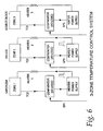
- FIG. 6 is a block diagram of a temperature control system which can be used in conjunction with the present invention.
- FIG. 1 is a cross-sectional schematic diagram of the ion source in accordance with the present invention which illustrates the construction and the functionality of the components which make up the ion source 10 .
- the cross section is cut along a plane which contains the direction of propagation of the ion beam, separating the ion source in two halves.
- the ion source 10 includes a vaporizer 28 and a beam forming region 12 joined together by at a mounting flange 36 .
- the ion source 10 is made to interface to an evacuated vacuum chamber of an ion implanter or other process tool by way of the mounting flange 36 .
- the portion of the ion source 10 to the right of the flange 36 in FIG. 1 is at high vacuum (pressure ⁇ 1 ⁇ 10 ⁇ 4 Torr).
- Gaseous material is introduced into an ionization chamber 44 where the gas molecules are ionized by electron impact from one or more electron beams 70 a and 70 b which enter the ionization chamber 44 through a pair of opposing electron beam entrance apertures 71 a and 71 b , respectively.
- ions are created adjacent to an ion extraction aperture 81 in an ion extraction aperture plate 80 .
- These ions are extracted and formed into an energetic ion beam by an extraction electrode (not shown) located in front of an ion extraction aperture plate 80 .
- FIG. 1 An exemplary vaporizer 28 is illustrated in FIG. 1 .
- the vaporizer 28 is exemplary and may be formed from a vaporizer body 30 and a crucible 31 for carrying a solid source feed material 29 , for example, decaborane, B 10 H 14 . Resistive heaters may be embedded into the vaporizer body 30 . Water cooling channels 26 and convective gas cooling channels 27 may be configured to be in intimate contact with the vaporizer body 30 and used to provide a uniform operating temperature above room temperature to the crucible 31 .
- Thermal conduction between the crucible 31 and the temperature-controlled vaporizer body 30 may be provided by way of a pressurized gas, introduced by a gas feed 41 into a crucible-vaporizer body interface 34 , while the temperature of the vaporizer body 31 is monitored by a thermocouple.
- Vaporized decaborane B 10 H 14 or other vaporized material 50 collects in a crucible ballast volume 51 and passes through a vaporizer exit bore 39 , through a pair of isolation valves 100 and 110 , and through a vapor conduit 32 , contained in a source block 35 , and enters the ionization chamber 44 through a vapor entrance aperture 33 .
- the isolation valves 100 , 110 , mounting flange 36 , and the source block 35 may also be temperature controlled to a temperature near or above the vaporizer temperature to prevent condensation of the vapor.
- the ion source gas delivery system may include two conduits that feed the ionization chamber 44 from two separate sources.
- the first source may be a small diameter low-conductance path which feeds gaseous material from a pressurized gas source, such as a gas cylinder (not shown).
- the second source may be from a high-conductance path from a low-temperature vaporizer, which vaporizes solid material.
- the gas delivery system maintains a gas pressure of, for example, a few millitorr, in the ionization chamber 44 .
- the vaporizer 28 maintains tight temperature control of its surfaces which are in contact with the solid material, in order to maintain a stable flow of gas into the ionization chamber, and hence a stable pressure within said chamber.
- the isolation valve 110 Prior to servicing the vaporizer 28 , the isolation valve 110 can be closed to keep the ion source and the ion implanter under vacuum.
- the isolation valve 100 can also be closed to maintain containment of the vapor 50 within the crucible 31 .
- the vaporizer 28 can then be transported safely to a chemical hood, where the crucible 31 can be recharged or cleaned.
- a vent valve 111 Prior to opening the valve 100 , a vent valve 111 , which may be welded into the body of valve 100 , can be opened to bring the crucible volume to atmospheric pressure.
- valve 100 may be again closed and the vaporizer 28 may be mounted onto the ion source 10 by attaching the valve 100 to the valve 110 , and the vent valve 111 is then connected to a roughing line to evacuate the crucible 31 and the dead volume between the valve 100 and the valve 110 .
- the isolation valve 110 can then be opened if desired, without compromising the vacuum environment of the ion source and ion implanter.
- a vaporizer assembly 30 a is formed by a heated and cooled vaporizer body 30 and a removable crucible 34 . Access to the crucible 31 is possible by removing an end plate (not shown) on the back of the vaporizer 28 . Once the crucible 31 is removed from the vaporizer 28 , it can be recharged by removing its cover 34 b that is elastomerically sealed to the end of the crucible 31 and raising a grate 34 a which isolates the solid 29 .
- the crucible 31 is inserted in the vaporizer body 30 and a vacuum seal is made to the exit bore 39 at the front of the vaporizer body 30 , to isolate the crucible ballast volume 51 from thermal transfer gas present within crucible-vaporizer body interface 34 .
- the bore 39 is used as the exit for the vaporized gas.
- the mechanical fit between the crucible 31 and the vaporizer body 30 is close, in order to achieve temperature uniformity of the crucible 31 .
- Any gap between the crucible 31 and the vaporizer body 30 may be filled with a gas to facilitate thermal transfer between the two surfaces.
- the thermal transfer gas enters said gap through an end plate fitting 28 a , and may be at or near atmospheric pressure.
- Temperature control may be performed using, for example, a proportional-integral differential (PID) closed-loop control of resistive elements that may be embedded in the vaporizer body 30 .
- FIG. 6 shows a block diagram of a preferred embodiment in which three temperature zones are defined: zone 1 for vaporizer body 30 , zone 2 for isolation valves 100 and 110 , and zone 3 for the source block 35 .
- Each zone may have a dedicated controller; for example, an Omron E5CK Digital Controller.
- heating elements alone are used to actively control temperature above room ambient, for example, between 18 C to 300 C or higher.
- resistive cartridge-type heaters can be embedded into the vaporizer body 30 (heater 1 ) the and the source block 35 (heater 3 ), while the valves 100 , 110 can be wrapped with silicone strip heaters (heater 2 ) in which the resistive elements are wire or foil strips.
- Three thermocouples labeled TC 1 , TC 2 , and TC 3 in FIG. 6 can be embedded into each of the three components 30 , 35 , 100 ( 110 ) and continuously read by each of the three dedicated temperature controllers.
- the temperature controllers 1 , 2 , and 3 are user-programmed with a temperature setpoint SP 1 , SP 2 , and SP 3 , respectively.
- the temperature setpoints are such that SP 3 >SP 2 >SP 1 .
- SP 2 might be 50 C and SP 3 70 C.
- the controllers typically operate such that when the TC readback does not match the setpoint, the controller's comparator initiates cooling or heating as required. For example, in the case where only heating is used to vary temperature, the comparator output is zero unless TC 1 ⁇ SP 1 .
- the controllers may contain a look-up table of output power as a nonlinear function of temperature difference SP 1 ⁇ TC 1 , and feed the appropriate signals to the controller's heater power supply in order to smoothly regulate temperature to the programmed setpoint value.
- a typical method of varying heater power is by pulse-width modulation of the power supply. This technique can be used to regulate power between 1% and 100% of full scale.
- Such PID controllers can typically hold temperature setpoint to within 0.2 C.
- the vaporizer body material may be selected to be highly thermally conductive to maintain temperature uniformity.
- a small thermal leak may be intentionally applied to the vaporizer body 30 to improve control system stability and reduce settling time by using air channels located on the outside surface of the vaporizer body 30 .
- the air channels 27 surround the vaporizer body 30 and are covered by plates (not shown). Air may be ducted to the channels within a manifold system, integrated into a vaporizer end plate (not shown) to provide moderate, continuous convective cooling. The air is fed through the inlet after proceeding past a metering valve used for flow control. The air discharges from the air assembly into house exhaust.
- a coolant may be ducted through a, for example, 1 meter long, 6 mm diameter bore that travels back and forth throughout the vaporizer body 30 . Connections may be made through fittings mounted to the body ports 26 .
- the liquid cooling provides rapid cooling of the vaporizer assembly to provide quick service turnaround when required.
- Gases may be fed into the ionization chamber 44 via a gas conduit 33 , for example, from a pressurized gas cylinder.
- Solid feed materials can be vaporized in the vaporizer 28 , and the vapor fed into ionization chamber 44 through the vapor conduit 32 , described above.
- Solid feed material 29 located under the perforated separation barrier 34 a , is held at a uniform temperature by temperature control of the vaporizer body 30 , as discussed above.
- Vapor 50 which accumulates in ballast volume 31 feeds through the bore 39 and through the shutoff valves 100 and 110 and, in turn, is fed into the ionization chamber 44 by way of a vapor conduit 32 , located in the source block 35 .
- both gaseous and solid dopant-bearing materials may be ionized by this ion source.
- FIG. 2 is a cross-sectional side view which illustrates the fundamental optical design of a multiple electron-beam ion source configuration in accordance with the present invention.
- a pair of spatially separate electron beams 70 a and 70 b are emitted from a pair of spatially separate heated filaments 110 a and 110 b and execute 90 degree trajectories due to the influence of beam steerers or static magnetic fields B 135 a and 135 b (in a direction normal to the plane of the paper as indicated) into the ionization chamber 44 , passing first through a pair of base plate apertures 106 a and 106 b and a pair of spaced apart base plates 105 a and 105 b , and then through a pair of electron entrance apertures 71 a and 71 b .
- Electrons passing all the way through the ionization chamber 44 are bent toward a pair of emitter shields 102 a and 102 b by the beam steerers, or static magnetic fields 135 a and 135 b .
- the electron beams propagate through the base plate apertures 106 a and 106 b , they are decelerate prior to entering ionization chamber 44 by the application of a voltage Va to the base plates 105 a and 105 b (provided by positive-going power supply 115 ), and voltage Ve to the filaments 135 a and 135 b (provided by negative-going power supply 116 ).
- Voltages are all relative to the ionization chamber 44 .
- the energy of the electron beam is therefore given by e(Va ⁇ Ve), where e is the electronic charge (6.02 ⁇ 10 ⁇ 19 Coulombs).
- the electron beam 70 a , 70 b is formed and deflected at an energy of 2 keV, but upon entering electron entrance aperture 71 a , 71 b it has an energy of only 0.5 keV.
- Electron Energy E Magnetic Field B 1500 eV 51 G 2000 eV 59 G 2500 eV 66 G
- FIG. 2 Other elements shown in FIG. 2 include an extracted ion beam 120 , a source electrostatic shield 101 , and a pair of emitter shields 102 a and 102 b .
- These emitter shields 102 a and 102 b serve two purposes: to provide shielding from electromagnetic fields, and to provide shielding from stray electron or ion beams.
- the emitter shields 102 a and 102 b shield the electron beams 70 a and 70 b from fields associated with the potential difference between base plates 105 a and 105 b and the source shield 101 , and also acts as a dump for stray electron beams from the opposing electron emitter.
- the source shield 101 shields the ion beam 120 from fields generated by the potential difference between base plates 105 a and 105 b and the ionization chamber 44 , and also acts to absorb stray electrons and ions which would otherwise impact the ion source elements. For this reason, both of the emitter shields 102 a and 102 b , as well as the source shield 101 , are constructed of refractory metal, such as molybdenum or graphite. Alternatively, more complete shielding of the ion beam 120 from the magnetic fields B 135 a and 135 b may be accomplished by constructing the source shield 101 of a ferromagnetic substance, such as magnetic stainless steel.
- FIG. 3 is a cutaway view illustrating the mechanical detail and which shows explicitly how the contents of FIG. 2 are incorporated into the ion source of FIG. 1 .
- Electrons are thermionically emitted from one or more of the filaments 110 a and 110 b and accelerated to a pair of corresponding anodes 140 a and 140 b forming the electron beams 70 a and 70 b .
- Such a configuration offers several benefits.
- the filaments 110 a and 110 b can be operated separately or together.
- the emitter life is extended relative to known configurations, since the emitter is in the low-pressure environment of the implanter vacuum housing in watch the ion source resides, and since the emitter is also effectively protected from ion bombardment.
- Magnetic flux from a pair of permanent magnets 130 a and 130 b and a pair of magnetic pole assemblies 125 a and 125 b is used to form beam steerers used to establish uniform magnetic fields across the air gap between the ends of the magnetic pole assemblies 125 a , 125 b , wherein the electron beam 70 a , 70 b propagates.
- the magnetic fields 135 a and 135 b and the electron beam energies of electron beams 70 a and 70 b are matched such that electron beams 70 a and 70 b are deflected 90 degrees, and pass into the ionization chamber 44 as shown.
- deflecting the electron beams 70 a and 70 b for example, through 90 degrees, no line of sight exists between the emitters and the ionization chamber 44 which contains the ions, thus preventing bombardment of the emitters by energetic charged particles.
- the electron beams 70 are decelerated as they pass through the gap defined by base plate apertures 106 a and 106 b and the electron entrance apertures 71 a and 71 b .
- the use of a decelerating lens allows the ionization energy of the electron beam to be adjusted without substantially affecting the electron beam generation and deflection.
- the gap may be established by one or more ceramic spacers 132 a and 132 b , which support each base plate 105 a and 105 b and act as a stand off from the source block 35 , which is at ionization chamber potential.
- the ceramic spacers 132 a and 132 b provide both electrical isolation and mechanical support. Note that for clarity, the emitter shields 102 and the source shield 101 are not shown in FIG. 3 .
- the baseplates 105 a and 105 b can intercept a portion of the energetic electron beams 70 a , 70 b .
- the baseplates 105 a , 105 b must therefore be either actively cooled, or passively cooled. Active cooling may be accomplished by passing liquid coolant, such as water, through the baseplates. Alternatively, passive cooling may be accomplished by allowing the baseplates to reach a temperature whereby they cool through radiation to their surroundings. This steady-state temperature depends on the intercepted beam power, the surface area and emissivity of the baseplates, and the temperatures of surrounding components. Allowing the baseplates 105 a , 105 b to operate at elevated temperature, for example at 200 C, may be advantageous when running condensable gases which can form contaminating and particle-forming films on cold surfaces.
- FIG. 4 shows a simplified top view of the electron beam-forming region of the source.
- the filament 110 b is at potential Ve, for example, ⁇ 0.5 keV with respect to the ionization chamber 44 (FIG. 3 ), and the anode 140 b , the magnetic pole assembly 125 b , the base plate 105 b , and the emitter shield 102 b are all at anode potential Va, for example, 1.5 keV.
- the electron beam energy is 2 keV.
- the electron beam 70 b is deflected by the magnetic field 135 b in the air gap between the poles of the magnetic pole assembly 125 b , such that the electron beam 70 b passes through the base plate aperture 106 b .
- Typical values for the base plate apertures 106 a and 106 b and the electron entrance apertures 71 a and 71 b are 1 cm in diameter, respectively.
- FIG. 5 illustrates how ionization probability depends on the electron energy for electron impact ionization.
- Ammonia NH 3
- Probability is expressed as cross section a, in units of 10 ⁇ 16 cm 2 .
- Electron energy (T) is in eV, i.e., electron-volts. Shown are two sets of theoretical curves marked BEB (vertical IP) and BEB (adiabatic IP) calculated from first principles, and two sets of experimental data, from Djuric et al. (1981) and from Rao and Srivastava (1992).
- FIG. 5 illustrates the fact that certain ranges of electron energies produce more ionization than in other energy ranges.
- cross sections are highest for electron impact energies between about 50 eV and 500 eV, peaking at about 100 eV.
- the energy with which the electron beams enter the ionization chamber 44 is an important parameter which affects the operation of the ion source of the present invention.
- the features shown in FIG. 2 through FIG. 4 show how the present invention incorporates electron optics which allow for broad control of electron impact ionization energy while operating at nearly constant conditions in the electron beam-forming and deflection regions of the ion source.
Abstract
Description
-
- Ionizing electron beams generated external to the ionization chamber, thereby extending the emitter lifetime.
- 90 degree magnetic deflection of electron beams such that no line-of-sight exists between the emitter and the process gas load, and the emitter is protected from bombardment by energetic charged particles.
- Two opposed electron beams which can be operated simultaneously or separately.
- Use of a deceleration lens to adjust the ionization energy of the electron beam, substantially without affecting electron beam generation and deflection.
| TABLE 1 |
| Dependence of Magnetic Field Strength on Electron Energy |
| to Accomplish a 90 Degree Deflection in the Present Invention |
| Electron Energy E | Magnetic Field B | ||
| 1500 eV | 51 G | ||
| 2000 eV | 59 G | ||
| 2500 eV | 66 G | ||
Claims (4)
Priority Applications (1)
| Application Number | Priority Date | Filing Date | Title |
|---|---|---|---|
| US10/748,078 US7023138B2 (en) | 2002-06-26 | 2003-12-30 | Electron impact ion source |
Applications Claiming Priority (2)
| Application Number | Priority Date | Filing Date | Title |
|---|---|---|---|
| US10/183,768 US6686595B2 (en) | 2002-06-26 | 2002-06-26 | Electron impact ion source |
| US10/748,078 US7023138B2 (en) | 2002-06-26 | 2003-12-30 | Electron impact ion source |
Related Parent Applications (1)
| Application Number | Title | Priority Date | Filing Date |
|---|---|---|---|
| US10/183,768 Continuation US6686595B2 (en) | 2002-06-26 | 2002-06-26 | Electron impact ion source |
Publications (2)
| Publication Number | Publication Date |
|---|---|
| US20040195973A1 US20040195973A1 (en) | 2004-10-07 |
| US7023138B2 true US7023138B2 (en) | 2006-04-04 |
Family
ID=29779196
Family Applications (7)
| Application Number | Title | Priority Date | Filing Date |
|---|---|---|---|
| US10/183,768 Expired - Fee Related US6686595B2 (en) | 2002-06-26 | 2002-06-26 | Electron impact ion source |
| US10/748,078 Expired - Fee Related US7023138B2 (en) | 2002-06-26 | 2003-12-30 | Electron impact ion source |
| US11/648,091 Abandoned US20070181830A1 (en) | 2002-06-26 | 2006-12-29 | Ion implantation device and a method of semiconductor manufacturing by the implantation of boron hydride cluster ions |
| US12/268,524 Expired - Fee Related US8071958B2 (en) | 2002-06-26 | 2008-11-11 | Ion implantation device and a method of semiconductor manufacturing by the implantation of boron hydride cluster ions |
| US13/102,321 Expired - Fee Related US8410459B2 (en) | 2002-06-26 | 2011-05-06 | Ion implantation device and a method of semiconductor manufacturing by the implantation of boron hydride cluster ions |
| US13/287,259 Expired - Fee Related US8618514B2 (en) | 2002-06-26 | 2011-11-02 | Ion implantation device and a method of semiconductor manufacturing by the implantation of boron hydride cluster ions |
| US14/073,565 Abandoned US20140061816A1 (en) | 2002-06-26 | 2013-11-06 | Ion implantation device and a method of semiconductor manufacturing by the implantation of boron hydride cluster ions |
Family Applications Before (1)
| Application Number | Title | Priority Date | Filing Date |
|---|---|---|---|
| US10/183,768 Expired - Fee Related US6686595B2 (en) | 2002-06-26 | 2002-06-26 | Electron impact ion source |
Family Applications After (5)
| Application Number | Title | Priority Date | Filing Date |
|---|---|---|---|
| US11/648,091 Abandoned US20070181830A1 (en) | 2002-06-26 | 2006-12-29 | Ion implantation device and a method of semiconductor manufacturing by the implantation of boron hydride cluster ions |
| US12/268,524 Expired - Fee Related US8071958B2 (en) | 2002-06-26 | 2008-11-11 | Ion implantation device and a method of semiconductor manufacturing by the implantation of boron hydride cluster ions |
| US13/102,321 Expired - Fee Related US8410459B2 (en) | 2002-06-26 | 2011-05-06 | Ion implantation device and a method of semiconductor manufacturing by the implantation of boron hydride cluster ions |
| US13/287,259 Expired - Fee Related US8618514B2 (en) | 2002-06-26 | 2011-11-02 | Ion implantation device and a method of semiconductor manufacturing by the implantation of boron hydride cluster ions |
| US14/073,565 Abandoned US20140061816A1 (en) | 2002-06-26 | 2013-11-06 | Ion implantation device and a method of semiconductor manufacturing by the implantation of boron hydride cluster ions |
Country Status (2)
| Country | Link |
|---|---|
| US (7) | US6686595B2 (en) |
| CN (1) | CN1973346B (en) |
Cited By (4)
| Publication number | Priority date | Publication date | Assignee | Title |
|---|---|---|---|---|
| US20060097193A1 (en) * | 2002-06-26 | 2006-05-11 | Horsky Thomas N | Ion implantation device and a method of semiconductor manufacturing by the implantation of boron hydride cluster ions |
| US20080047487A1 (en) * | 2006-07-14 | 2008-02-28 | Georgia Tech Research Corporation | In-situ flux measurement devices, methods, and systems |
| US20080305598A1 (en) * | 2007-06-07 | 2008-12-11 | Horsky Thomas N | Ion implantation device and a method of semiconductor manufacturing by the implantation of ions derived from carborane molecular species |
| US20090090872A1 (en) * | 2002-06-26 | 2009-04-09 | Horsky Thomas N | Ion implantation device and a method of semiconductor manufacturing by the implantation of boron hydride cluster ions |
Families Citing this family (69)
| Publication number | Priority date | Publication date | Assignee | Title |
|---|---|---|---|---|
| US7838842B2 (en) * | 1999-12-13 | 2010-11-23 | Semequip, Inc. | Dual mode ion source for ion implantation |
| US20040002202A1 (en) * | 2002-06-26 | 2004-01-01 | Horsky Thomas Neil | Method of manufacturing CMOS devices by the implantation of N- and P-type cluster ions |
| US7697673B2 (en) * | 2003-11-17 | 2010-04-13 | Apptera Inc. | System for advertisement selection, placement and delivery within a multiple-tenant voice interaction service system |
| US7206391B2 (en) * | 2003-12-23 | 2007-04-17 | Apptera Inc. | Method for creating and deploying system changes in a voice application system |
| WO2005059942A2 (en) * | 2003-12-12 | 2005-06-30 | Semequip, Inc. | Method and apparatus for extending equipment uptime in ion implantation |
| US7791047B2 (en) * | 2003-12-12 | 2010-09-07 | Semequip, Inc. | Method and apparatus for extracting ions from an ion source for use in ion implantation |
| US20080223409A1 (en) * | 2003-12-12 | 2008-09-18 | Horsky Thomas N | Method and apparatus for extending equipment uptime in ion implantation |
| US20080242066A1 (en) * | 2004-10-22 | 2008-10-02 | Semiequip Inc. | Method Of Manufacturing Semiconductor |
| FR2878863B1 (en) * | 2004-12-07 | 2007-11-23 | Addon Sa | VACUUM DEPOSITION DEVICE WITH RECHARGEABLE RESERVOIR AND CORRESPONDING VACUUM DEPOSITION METHOD. |
| KR101246186B1 (en) * | 2005-05-20 | 2013-03-21 | 베리안 세미콘덕터 이큅먼트 어소시에이츠, 인크. | A resonance method for production of intense low-impurity ion beams of atoms and molecules |
| US7365340B2 (en) * | 2005-07-20 | 2008-04-29 | Varian Semiconductor Equipment Associates, Inc. | Resonance method for production of intense low-impurity ion beams of atoms and molecules |
| US7372195B2 (en) * | 2005-09-10 | 2008-05-13 | Applied Materials, Inc. | Electron beam source having an extraction electrode provided with a magnetic disk element |
| KR101455404B1 (en) | 2005-12-09 | 2014-10-27 | 세미이큅, 인코포레이티드 | System and method for the manufacture of semiconductor devices by the implantation of carbon clusters |
| US20070178679A1 (en) * | 2006-01-28 | 2007-08-02 | Varian Semiconductor Equipment Associates, Inc. | Methods of implanting ions and ion sources used for same |
| US20070178678A1 (en) * | 2006-01-28 | 2007-08-02 | Varian Semiconductor Equipment Associates, Inc. | Methods of implanting ions and ion sources used for same |
| EP2026889A4 (en) * | 2006-06-12 | 2011-09-07 | Semequip Inc | Vapor delivery to devices under vacuum |
| JP4946256B2 (en) * | 2006-08-11 | 2012-06-06 | 日新イオン機器株式会社 | Electric field lens and ion implantation apparatus including the same |
| US7589333B2 (en) * | 2006-09-29 | 2009-09-15 | Axcelis Technologies, Inc. | Methods for rapidly switching off an ion beam |
| US8803110B2 (en) * | 2006-09-29 | 2014-08-12 | Axcelis Technologies, Inc. | Methods for beam current modulation by ion source parameter modulation |
| US8073681B2 (en) * | 2006-10-16 | 2011-12-06 | Voicebox Technologies, Inc. | System and method for a cooperative conversational voice user interface |
| US7605382B2 (en) * | 2006-10-31 | 2009-10-20 | Nissin Ion Equipment Co., Ltd. | Ion implanter |
| WO2008070453A2 (en) * | 2006-11-22 | 2008-06-12 | Semequip, Inc. | Vapor delivery system useful with ion sources and vaporizer for use in such system |
| US7919402B2 (en) * | 2006-12-06 | 2011-04-05 | Semequip, Inc. | Cluster ion implantation for defect engineering |
| US7883909B2 (en) * | 2006-12-28 | 2011-02-08 | Texas Instruments Incorporated | Method to measure ion beam angle |
| US7947966B2 (en) * | 2007-07-31 | 2011-05-24 | Axcelis Technologies, Inc. | Double plasma ion source |
| WO2009039382A1 (en) * | 2007-09-21 | 2009-03-26 | Semequip. Inc. | Method for extending equipment uptime in ion implantation |
| KR20090045767A (en) * | 2007-11-02 | 2009-05-08 | 삼성전자주식회사 | Perpendicular magnetic recording media and method of manufacturing the same |
| TWI413149B (en) * | 2008-01-22 | 2013-10-21 | Semequip Inc | Ion source gas reactor and method for converting a gaseous feed materital into a different molecular or atomic species |
| US8330118B2 (en) * | 2008-05-16 | 2012-12-11 | Semequip, Inc. | Multi mode ion source |
| US7759657B2 (en) | 2008-06-19 | 2010-07-20 | Axcelis Technologies, Inc. | Methods for implanting B22Hx and its ionized lower mass byproducts |
| KR101052361B1 (en) * | 2008-07-31 | 2011-07-27 | 한국표준과학연구원 | Spectrometer Using Heavy Energy Ion Beam Scattering |
| US20100177454A1 (en) * | 2009-01-09 | 2010-07-15 | Component Re-Engineering Company, Inc. | Electrostatic chuck with dielectric inserts |
| FR2943173B1 (en) * | 2009-03-11 | 2016-03-18 | Alcatel Lucent | IONIZATION CELL FOR MASS SPECTROMETER AND CORRESPONDING LEAK DETECTOR |
| US20100258431A1 (en) * | 2009-04-10 | 2010-10-14 | Applied Materials, Inc. | Use special ion source apparatus and implant with molecular ions to process hdd (high density magnetic disks) with patterned magnetic domains |
| US8487239B2 (en) * | 2009-05-29 | 2013-07-16 | Micromass Uk Limited | Mass spectrometer |
| KR101747473B1 (en) * | 2009-10-27 | 2017-06-27 | 엔테그리스, 아이엔씨. | Ion implantation system and method |
| CN102194635A (en) * | 2010-03-18 | 2011-09-21 | 上海凯世通半导体有限公司 | Ion implanting system and method |
| US8669539B2 (en) * | 2010-03-29 | 2014-03-11 | Advanced Ion Beam Technology, Inc. | Implant method and implanter by using a variable aperture |
| KR20130094697A (en) * | 2010-04-02 | 2013-08-26 | 인터디지탈 패튼 홀딩스, 인크 | Methods for policy management |
| US20120056107A1 (en) * | 2010-09-08 | 2012-03-08 | Varian Semiconductor Equipment Associates, Inc. | Uniformity control using ion beam blockers |
| CN102543873B (en) * | 2010-12-27 | 2015-08-19 | 无锡华润上华科技有限公司 | Autoregistration P+ shallow junction doping process |
| US8907307B2 (en) * | 2011-03-11 | 2014-12-09 | Varian Semiconductor Equipment Associates, Inc. | Apparatus and method for maskless patterned implantation |
| JP5975418B2 (en) | 2011-03-25 | 2016-08-23 | 日新イオン機器株式会社 | Ion implantation method |
| KR20130054010A (en) * | 2011-11-16 | 2013-05-24 | 삼성전자주식회사 | Semiconductor device using iii-v group material and method of manufacturing the same |
| US8963107B2 (en) * | 2012-01-12 | 2015-02-24 | Axcelis Technologies, Inc. | Beam line design to reduce energy contamination |
| US9490185B2 (en) * | 2012-08-31 | 2016-11-08 | Axcelis Technologies, Inc. | Implant-induced damage control in ion implantation |
| US9484176B2 (en) * | 2012-09-10 | 2016-11-01 | Thomas Schenkel | Advanced penning ion source |
| US9134074B2 (en) * | 2012-10-04 | 2015-09-15 | Varian Semiconductor Equipment Associates, Inc. | Method and apparatus for thermal control of ion sources and sputtering targets |
| KR101366781B1 (en) * | 2012-11-12 | 2014-02-21 | 한국표준과학연구원 | Ion source and mass spectrometer having the same |
| GB2562170B (en) * | 2013-02-19 | 2019-02-06 | Markes International Ltd | A method of ionising analyte molecules for analysis |
| GB2518122B (en) | 2013-02-19 | 2018-08-08 | Markes International Ltd | An electron ionisation apparatus |
| US9865422B2 (en) * | 2013-03-15 | 2018-01-09 | Nissin Ion Equipment Co., Ltd. | Plasma generator with at least one non-metallic component |
| US9315892B2 (en) * | 2013-03-15 | 2016-04-19 | Taiwan Semiconductor Manufacturing Company Limited | Method and apparatus for controlling beam angle during ion implantation of a semiconductor wafer based upon pressure |
| US9502213B2 (en) | 2013-03-15 | 2016-11-22 | Nissin Ion Equipment Co., Ltd. | Ion beam line |
| CN105247660B (en) | 2013-03-15 | 2018-06-12 | 格伦·莱恩家族有限责任有限合伙企业 | Scalable quality resolving aperture |
| US8994272B2 (en) | 2013-03-15 | 2015-03-31 | Nissin Ion Equipment Co., Ltd. | Ion source having at least one electron gun comprising a gas inlet and a plasma region defined by an anode and a ground element thereof |
| US9142386B2 (en) | 2013-03-15 | 2015-09-22 | Nissin Ion Equipment Co., Ltd. | Ion beam line |
| US9275819B2 (en) | 2013-03-15 | 2016-03-01 | Nissin Ion Equipment Co., Ltd. | Magnetic field sources for an ion source |
| US9418827B2 (en) * | 2013-07-23 | 2016-08-16 | Hamilton Sundstrand Corporation | Methods of ion source fabrication |
| JP6257455B2 (en) * | 2014-06-17 | 2018-01-10 | 住友重機械イオンテクノロジー株式会社 | Ion implantation apparatus and control method of ion implantation apparatus |
| US20160133711A1 (en) * | 2014-11-06 | 2016-05-12 | Inotera Memories, Inc. | Method of fabricating source/drain region and semiconductor structure having source/drain region fabricated by the same |
| CN104483615B (en) * | 2014-12-24 | 2017-10-24 | 上海华虹宏力半导体制造有限公司 | Trench grate MOS device defect verification method |
| JP6545053B2 (en) * | 2015-03-30 | 2019-07-17 | 東京エレクトロン株式会社 | Processing apparatus and processing method, and gas cluster generating apparatus and generating method |
| US10969370B2 (en) * | 2015-06-05 | 2021-04-06 | Semilab Semiconductor Physics Laboratory Co., Ltd. | Measuring semiconductor doping using constant surface potential corona charging |
| CN108962734B (en) * | 2018-06-27 | 2021-01-01 | 武汉华星光电半导体显示技术有限公司 | Preparation method of polycrystalline silicon semiconductor layer, thin film transistor and preparation method |
| CN108906363B (en) * | 2018-07-13 | 2023-08-01 | 金华职业技术学院 | Vacuum deposition method of organic molecules |
| US11164722B2 (en) * | 2018-07-31 | 2021-11-02 | Taiwan Semiconductor Manufacturing Co., Ltd. | Ion implantation method |
| US10573485B1 (en) * | 2018-12-20 | 2020-02-25 | Axcelis Technologies, Inc. | Tetrode extraction apparatus for ion source |
| WO2022256295A1 (en) * | 2021-06-01 | 2022-12-08 | Inficon, Inc. | Method of detecting radicals using mass spectrometry |
Citations (21)
| Publication number | Priority date | Publication date | Assignee | Title |
|---|---|---|---|---|
| US3557365A (en) | 1967-12-22 | 1971-01-19 | Perkin Elmer Corp | Ion source for a mass spectrometer |
| US3581195A (en) | 1968-06-10 | 1971-05-25 | Varian Associates | Detection of vacuum leaks by gas ionization method and apparatus providing decreased vacuum recovery time |
| US4120700A (en) | 1975-12-30 | 1978-10-17 | Futaba Denshi Kogyo Kabushiki Kaisha | Method of producing p-n junction type elements by ionized cluster beam deposition and ion-implantation |
| US4152478A (en) | 1974-10-23 | 1979-05-01 | Futaba Denshi Kogyo Kabushiki Kaisha | Ionized-cluster deposited on a substrate and method of depositing ionized cluster on a substrate |
| US4217855A (en) | 1974-10-23 | 1980-08-19 | Futaba Denshi Kogyo K.K. | Vaporized-metal cluster ion source and ionized-cluster beam deposition device |
| US4649278A (en) | 1985-05-02 | 1987-03-10 | The United States Of America As Represented By The Administrator Of The National Aeronautics And Space Administration | Generation of intense negative ion beams |
| US4686365A (en) * | 1984-12-24 | 1987-08-11 | American Cyanamid Company | Fourier transform ion cyclothon resonance mass spectrometer with spatially separated sources and detector |
| US4740698A (en) | 1986-03-26 | 1988-04-26 | Hitachi, Ltd. | Hybrid charged particle apparatus |
| US4788024A (en) * | 1986-02-24 | 1988-11-29 | Aneutronic Energy Labs, Inc. | Apparatus and method for obtaining a self-colliding beam of charged particles operating above the space charge limit |
| US4943718A (en) | 1988-02-18 | 1990-07-24 | Vg Instruments Group Limited | Mass spectrometer |
| US5101105A (en) * | 1990-11-02 | 1992-03-31 | Univeristy Of Maryland, Baltimore County | Neutralization/chemical reionization tandem mass spectrometry method and apparatus therefor |
| US5104684A (en) * | 1990-05-25 | 1992-04-14 | Massachusetts Institute Of Technology | Ion beam induced deposition of metals |
| US5136171A (en) * | 1990-03-02 | 1992-08-04 | Varian Associates, Inc. | Charge neutralization apparatus for ion implantation system |
| US5528034A (en) | 1994-09-28 | 1996-06-18 | The University Of Tokyo | Method of ultra high sensitivity hydrogen detection with slow multiply-charged ions |
| US5543625A (en) | 1994-05-20 | 1996-08-06 | Finnigan Corporation | Filament assembly for mass spectrometer ion sources |
| US5561326A (en) | 1992-01-08 | 1996-10-01 | Mitsubishi Denki Kabushiki Kaisha | Large scale integrated circuit device |
| US5686789A (en) | 1995-03-14 | 1997-11-11 | Osram Sylvania Inc. | Discharge device having cathode with micro hollow array |
| US6288403B1 (en) | 1999-10-11 | 2001-09-11 | Axcelis Technologies, Inc. | Decaborane ionizer |
| US6352626B1 (en) | 1999-04-19 | 2002-03-05 | Von Zweck Heimart | Sputter ion source for boron and other targets |
| US20020070672A1 (en) | 1999-12-13 | 2002-06-13 | Horsky Thomas N. | Electron beam ion source with integral low-temperature vaporizer |
| US20030001095A1 (en) | 2001-07-02 | 2003-01-02 | Schlumberger Technologies, Inc. | Method and apparatus for multiple charged particle beams |
Family Cites Families (73)
| Publication number | Priority date | Publication date | Assignee | Title |
|---|---|---|---|---|
| US603956A (en) * | 1898-05-10 | Wheel tire and felly | ||
| US3654457A (en) * | 1968-02-12 | 1972-04-04 | Hitachi Ltd | Ion source device equipped with sample heating means for use in mass spectrometer |
| DE1915692A1 (en) * | 1968-04-01 | 1969-12-18 | Ceskoslovenska Akademie Ved | Process for doping the semiconductor crystals and semiconductor layers |
| US3915757A (en) * | 1972-08-09 | 1975-10-28 | Niels N Engel | Ion plating method and product therefrom |
| US3908183A (en) * | 1973-03-14 | 1975-09-23 | California Linear Circuits Inc | Combined ion implantation and kinetic transport deposition process |
| JPS51115852A (en) * | 1975-04-04 | 1976-10-12 | Nissan Motor Co Ltd | Detector of the revolving angle and revolution of a revolving body |
| DE2610165C2 (en) * | 1976-03-11 | 1983-11-10 | Gesellschaft für Schwerionenforschung mbH, 6100 Darmstadt | Duoplasmatron ion source for generating multiply charged ions |
| US4112306A (en) * | 1976-12-06 | 1978-09-05 | Varian Associates, Inc. | Neutron irradiation therapy machine |
| JPS5593641A (en) | 1979-01-08 | 1980-07-16 | Hitachi Ltd | Electromagnetic focussing cathode ray tube |
| JPS5672423A (en) * | 1979-11-16 | 1981-06-16 | Canon Inc | Electromagnetic-drive slit exposure shutter |
| US4412900A (en) * | 1981-03-13 | 1983-11-01 | Hitachi, Ltd. | Method of manufacturing photosensors |
| US4366459A (en) * | 1981-07-09 | 1982-12-28 | Hi-G Incorporated | Miniature magnetic latch relay |
| US4587432A (en) * | 1984-08-03 | 1986-05-06 | Applied Materials, Inc. | Apparatus for ion implantation |
| FR2611975B1 (en) * | 1987-03-03 | 1995-02-17 | Commissariat Energie Atomique | PERMANENT MAGNET SYSTEM FOR AN INTENSE MAGNETIC FIELD |
| JPH0191431A (en) * | 1987-04-16 | 1989-04-11 | Sumitomo Eaton Noba Kk | Detector for electrostatic charge amount on wafer in ion implanting device |
| CN1020028C (en) * | 1987-08-18 | 1993-03-03 | 联邦德国Itt工业股份有限公司 | Method of fabricating implanted wells and islands of cmos integrated circuits |
| JPH01225117A (en) | 1988-03-04 | 1989-09-08 | Nippon Telegr & Teleph Corp <Ntt> | Method and device for manufacturing semiconductor device |
| US5313061A (en) * | 1989-06-06 | 1994-05-17 | Viking Instrument | Miniaturized mass spectrometer system |
| JPH0552495A (en) | 1991-08-28 | 1993-03-02 | Toshiba Corp | Flight control system |
| JPH05106037A (en) * | 1991-10-16 | 1993-04-27 | Mitsubishi Electric Corp | Ion implantation device and controlling method therefor |
| JPH0793125B2 (en) | 1992-05-13 | 1995-10-09 | 日新ハイボルテージ株式会社 | Negative ion implantation method |
| KR0131723B1 (en) | 1994-06-08 | 1998-04-14 | 김주용 | Manufacturing method for semiconductor device |
| JPH0817376A (en) | 1994-07-01 | 1996-01-19 | Mitsubishi Electric Corp | Ion source and ion implanter |
| US5489550A (en) * | 1994-08-09 | 1996-02-06 | Texas Instruments Incorporated | Gas-phase doping method using germanium-containing additive |
| US5672879A (en) * | 1995-06-12 | 1997-09-30 | Glavish; Hilton F. | System and method for producing superimposed static and time-varying magnetic fields |
| US5993766A (en) * | 1996-05-20 | 1999-11-30 | Advanced Technology Materials, Inc. | Gas source and dispensing system |
| JPH09312099A (en) | 1996-05-21 | 1997-12-02 | Toshiba Microelectron Corp | Semiconductor memory and its accessing method |
| JP3749924B2 (en) * | 1996-12-03 | 2006-03-01 | 富士通株式会社 | Ion implantation method and semiconductor device manufacturing method |
| US5998838A (en) * | 1997-03-03 | 1999-12-07 | Nec Corporation | Thin film transistor |
| US6013546A (en) | 1997-12-19 | 2000-01-11 | Advanced Micro Devices, Inc. | Semiconductor device having a PMOS device with a source/drain region formed using a heavy atom p-type implant and method of manufacture thereof |
| US5945704A (en) | 1998-04-06 | 1999-08-31 | Siemens Aktiengesellschaft | Trench capacitor with epi buried layer |
| US6093594A (en) * | 1998-04-29 | 2000-07-25 | Advanced Micro Devices, Inc. | CMOS optimization method utilizing sacrificial sidewall spacer |
| TW473834B (en) * | 1998-05-01 | 2002-01-21 | Ibm | Method of doping a gate and creating a very shallow source/drain extension and resulting semiconductor |
| US6403956B1 (en) | 1998-05-01 | 2002-06-11 | California Institute Of Technology | Temperature compensation for miniaturized magnetic sector |
| US6351010B1 (en) * | 1998-09-22 | 2002-02-26 | Sony Corporation | Electrooptical device, substrate for driving electrooptical device and methods for making the same |
| US6232208B1 (en) | 1998-11-06 | 2001-05-15 | Advanced Micro Devices, Inc. | Semiconductor device and method of manufacturing a semiconductor device having an improved gate electrode profile |
| AU2430601A (en) * | 1999-12-13 | 2001-06-18 | Semequip, Inc. | Ion implantation ion source, system and method |
| ITSV20000023A1 (en) * | 2000-06-15 | 2001-12-15 | Esaote Spa | PROCEDURE FOR THE PRODUCTION OF MAGNETIC FIELD GENERATION DEVICES IN MACHINES FOR THE DETECTION OF IMAGES IN RESONANCE |
| US6893907B2 (en) * | 2002-06-05 | 2005-05-17 | Applied Materials, Inc. | Fabrication of silicon-on-insulator structure using plasma immersion ion implantation |
| US7037813B2 (en) * | 2000-08-11 | 2006-05-02 | Applied Materials, Inc. | Plasma immersion ion implantation process using a capacitively coupled plasma source having low dissociation and low minimum plasma voltage |
| US6479828B2 (en) | 2000-12-15 | 2002-11-12 | Axcelis Tech Inc | Method and system for icosaborane implantation |
| US7023128B2 (en) * | 2001-04-20 | 2006-04-04 | Applied Process Technologies, Inc. | Dipole ion source |
| US6830979B2 (en) * | 2001-05-23 | 2004-12-14 | Matsushita Electric Industrial Co., Ltd. | Method for fabricating semiconductor device |
| JP3824058B2 (en) | 2001-05-23 | 2006-09-20 | 独立行政法人産業技術総合研究所 | Carborane super cluster and manufacturing method thereof |
| KR100429873B1 (en) * | 2001-07-19 | 2004-05-04 | 삼성전자주식회사 | MOS transistor and forming method thereof |
| US20030030010A1 (en) * | 2001-08-07 | 2003-02-13 | Perel Alexander S. | Decaborane vaporizer having improved vapor flow |
| US20030111014A1 (en) * | 2001-12-18 | 2003-06-19 | Donatucci Matthew B. | Vaporizer/delivery vessel for volatile/thermally sensitive solid and liquid compounds |
| US7518124B2 (en) | 2002-03-28 | 2009-04-14 | Applied Materials, Inc. | Monatomic dopant ion source and method |
| GB2387022B (en) | 2002-03-28 | 2005-12-21 | Applied Materials Inc | Monatomic boron ion source and method |
| WO2004003970A2 (en) * | 2002-06-26 | 2004-01-08 | Semequip Inc. | A semiconductor device and method of fabricating a semiconductor device |
| CN102034665B (en) | 2002-06-26 | 2014-06-25 | 山米奎普公司 | An ion implantation device and a method of semiconductor manufacturing by the implantation of boron hydride cluster ions |
| US20040002202A1 (en) * | 2002-06-26 | 2004-01-01 | Horsky Thomas Neil | Method of manufacturing CMOS devices by the implantation of N- and P-type cluster ions |
| US6686595B2 (en) | 2002-06-26 | 2004-02-03 | Semequip Inc. | Electron impact ion source |
| US7300038B2 (en) * | 2002-07-23 | 2007-11-27 | Advanced Technology Materials, Inc. | Method and apparatus to help promote contact of gas with vaporized material |
| US6812073B2 (en) * | 2002-12-10 | 2004-11-02 | Texas Instrument Incorporated | Source drain and extension dopant concentration |
| US7410890B2 (en) | 2002-12-12 | 2008-08-12 | Tel Epion Inc. | Formation of doped regions and/or ultra-shallow junctions in semiconductor materials by gas-cluster ion irradiation |
| US20080200020A1 (en) * | 2003-06-18 | 2008-08-21 | Semequip, Inc. | Semiconductor device and method of fabricating a semiconductor device |
| US6995079B2 (en) | 2003-08-29 | 2006-02-07 | Semiconductor Energy Laboratory Co., Ltd. | Ion implantation method and method for manufacturing semiconductor device |
| US7791047B2 (en) * | 2003-12-12 | 2010-09-07 | Semequip, Inc. | Method and apparatus for extracting ions from an ion source for use in ion implantation |
| WO2005074586A2 (en) | 2004-02-02 | 2005-08-18 | Semequip Inc. | Method of production of b10h102- ammonium salts and methods of production of b18h22 |
| US7112789B2 (en) * | 2004-05-18 | 2006-09-26 | White Nicholas R | High aspect ratio, high mass resolution analyzer magnet and system for ribbon ion beams |
| US7122435B2 (en) * | 2004-08-02 | 2006-10-17 | Texas Instruments Incorporated | Methods, systems and structures for forming improved transistors |
| US20060144332A1 (en) | 2005-01-04 | 2006-07-06 | Sweeney Joseph D | Controlled flow of source material via droplet evaporation |
| US7098099B1 (en) * | 2005-02-24 | 2006-08-29 | Texas Instruments Incorporated | Semiconductor device having optimized shallow junction geometries and method for fabrication thereof |
| US7385208B2 (en) * | 2005-07-07 | 2008-06-10 | Taiwan Semiconductor Manufacturing Co., Ltd. | Systems and methods for implant dosage control |
| KR101455404B1 (en) * | 2005-12-09 | 2014-10-27 | 세미이큅, 인코포레이티드 | System and method for the manufacture of semiconductor devices by the implantation of carbon clusters |
| US20070178678A1 (en) | 2006-01-28 | 2007-08-02 | Varian Semiconductor Equipment Associates, Inc. | Methods of implanting ions and ion sources used for same |
| US8586459B2 (en) * | 2006-11-06 | 2013-11-19 | Semequip, Inc. | Ion implantation with molecular ions containing phosphorus and arsenic |
| US7928406B2 (en) * | 2007-05-22 | 2011-04-19 | Semequip, Inc. | Method and system for extracting ion beams composed of molecular ions (cluster ion beam extraction system) |
| US20080305598A1 (en) * | 2007-06-07 | 2008-12-11 | Horsky Thomas N | Ion implantation device and a method of semiconductor manufacturing by the implantation of ions derived from carborane molecular species |
| US8330118B2 (en) * | 2008-05-16 | 2012-12-11 | Semequip, Inc. | Multi mode ion source |
| JP2011523764A (en) * | 2008-05-30 | 2011-08-18 | アクセリス テクノロジーズ, インコーポレイテッド | Control of particles in a semiconductor wafer when borohydride is implanted into the semiconductor wafer |
| US7759657B2 (en) | 2008-06-19 | 2010-07-20 | Axcelis Technologies, Inc. | Methods for implanting B22Hx and its ionized lower mass byproducts |
-
2002
- 2002-06-26 US US10/183,768 patent/US6686595B2/en not_active Expired - Fee Related
-
2003
- 2003-06-26 CN CN03815031XA patent/CN1973346B/en not_active Expired - Fee Related
- 2003-12-30 US US10/748,078 patent/US7023138B2/en not_active Expired - Fee Related
-
2006
- 2006-12-29 US US11/648,091 patent/US20070181830A1/en not_active Abandoned
-
2008
- 2008-11-11 US US12/268,524 patent/US8071958B2/en not_active Expired - Fee Related
-
2011
- 2011-05-06 US US13/102,321 patent/US8410459B2/en not_active Expired - Fee Related
- 2011-11-02 US US13/287,259 patent/US8618514B2/en not_active Expired - Fee Related
-
2013
- 2013-11-06 US US14/073,565 patent/US20140061816A1/en not_active Abandoned
Patent Citations (22)
| Publication number | Priority date | Publication date | Assignee | Title |
|---|---|---|---|---|
| US3557365A (en) | 1967-12-22 | 1971-01-19 | Perkin Elmer Corp | Ion source for a mass spectrometer |
| US3581195A (en) | 1968-06-10 | 1971-05-25 | Varian Associates | Detection of vacuum leaks by gas ionization method and apparatus providing decreased vacuum recovery time |
| US4152478A (en) | 1974-10-23 | 1979-05-01 | Futaba Denshi Kogyo Kabushiki Kaisha | Ionized-cluster deposited on a substrate and method of depositing ionized cluster on a substrate |
| US4217855A (en) | 1974-10-23 | 1980-08-19 | Futaba Denshi Kogyo K.K. | Vaporized-metal cluster ion source and ionized-cluster beam deposition device |
| US4120700A (en) | 1975-12-30 | 1978-10-17 | Futaba Denshi Kogyo Kabushiki Kaisha | Method of producing p-n junction type elements by ionized cluster beam deposition and ion-implantation |
| US4686365A (en) * | 1984-12-24 | 1987-08-11 | American Cyanamid Company | Fourier transform ion cyclothon resonance mass spectrometer with spatially separated sources and detector |
| US4649278A (en) | 1985-05-02 | 1987-03-10 | The United States Of America As Represented By The Administrator Of The National Aeronautics And Space Administration | Generation of intense negative ion beams |
| US4788024A (en) * | 1986-02-24 | 1988-11-29 | Aneutronic Energy Labs, Inc. | Apparatus and method for obtaining a self-colliding beam of charged particles operating above the space charge limit |
| US4740698A (en) | 1986-03-26 | 1988-04-26 | Hitachi, Ltd. | Hybrid charged particle apparatus |
| US4943718A (en) | 1988-02-18 | 1990-07-24 | Vg Instruments Group Limited | Mass spectrometer |
| US5136171A (en) * | 1990-03-02 | 1992-08-04 | Varian Associates, Inc. | Charge neutralization apparatus for ion implantation system |
| US5104684A (en) * | 1990-05-25 | 1992-04-14 | Massachusetts Institute Of Technology | Ion beam induced deposition of metals |
| US5101105A (en) * | 1990-11-02 | 1992-03-31 | Univeristy Of Maryland, Baltimore County | Neutralization/chemical reionization tandem mass spectrometry method and apparatus therefor |
| US5561326A (en) | 1992-01-08 | 1996-10-01 | Mitsubishi Denki Kabushiki Kaisha | Large scale integrated circuit device |
| US5543625A (en) | 1994-05-20 | 1996-08-06 | Finnigan Corporation | Filament assembly for mass spectrometer ion sources |
| US5528034A (en) | 1994-09-28 | 1996-06-18 | The University Of Tokyo | Method of ultra high sensitivity hydrogen detection with slow multiply-charged ions |
| US5686789A (en) | 1995-03-14 | 1997-11-11 | Osram Sylvania Inc. | Discharge device having cathode with micro hollow array |
| US6352626B1 (en) | 1999-04-19 | 2002-03-05 | Von Zweck Heimart | Sputter ion source for boron and other targets |
| US6288403B1 (en) | 1999-10-11 | 2001-09-11 | Axcelis Technologies, Inc. | Decaborane ionizer |
| US20020070672A1 (en) | 1999-12-13 | 2002-06-13 | Horsky Thomas N. | Electron beam ion source with integral low-temperature vaporizer |
| US6452338B1 (en) | 1999-12-13 | 2002-09-17 | Semequip, Inc. | Electron beam ion source with integral low-temperature vaporizer |
| US20030001095A1 (en) | 2001-07-02 | 2003-01-02 | Schlumberger Technologies, Inc. | Method and apparatus for multiple charged particle beams |
Non-Patent Citations (2)
| Title |
|---|
| Boggia et al., "Study of a Trapped Ion Source", IEEE Journal, pp. 1433-1435. |
| Brautti et al., "Trapped Ion Source", IEEE Journal 1998, pp. 2729-2731. |
Cited By (11)
| Publication number | Priority date | Publication date | Assignee | Title |
|---|---|---|---|---|
| US20060097193A1 (en) * | 2002-06-26 | 2006-05-11 | Horsky Thomas N | Ion implantation device and a method of semiconductor manufacturing by the implantation of boron hydride cluster ions |
| US20090090872A1 (en) * | 2002-06-26 | 2009-04-09 | Horsky Thomas N | Ion implantation device and a method of semiconductor manufacturing by the implantation of boron hydride cluster ions |
| US7960709B2 (en) | 2002-06-26 | 2011-06-14 | Semequip, Inc. | Ion implantation device and a method of semiconductor manufacturing by the implantation of boron hydride cluster ions |
| US8071958B2 (en) * | 2002-06-26 | 2011-12-06 | Semequip, Inc. | Ion implantation device and a method of semiconductor manufacturing by the implantation of boron hydride cluster ions |
| US8410459B2 (en) | 2002-06-26 | 2013-04-02 | Semequip, Inc. | Ion implantation device and a method of semiconductor manufacturing by the implantation of boron hydride cluster ions |
| US8618514B2 (en) | 2002-06-26 | 2013-12-31 | Semequip, Inc. | Ion implantation device and a method of semiconductor manufacturing by the implantation of boron hydride cluster ions |
| US20080047487A1 (en) * | 2006-07-14 | 2008-02-28 | Georgia Tech Research Corporation | In-situ flux measurement devices, methods, and systems |
| US8261690B2 (en) * | 2006-07-14 | 2012-09-11 | Georgia Tech Research Corporation | In-situ flux measurement devices, methods, and systems |
| US8360002B2 (en) * | 2006-07-14 | 2013-01-29 | Georgia Tech Research Corporation | In-situ flux measurement devices, methods, and systems |
| US8377518B2 (en) * | 2006-07-14 | 2013-02-19 | Georgia Tech Research Corporation | In-situ flux measurement devices, methods, and systems |
| US20080305598A1 (en) * | 2007-06-07 | 2008-12-11 | Horsky Thomas N | Ion implantation device and a method of semiconductor manufacturing by the implantation of ions derived from carborane molecular species |
Also Published As
| Publication number | Publication date |
|---|---|
| US20140061816A1 (en) | 2014-03-06 |
| US6686595B2 (en) | 2004-02-03 |
| US8071958B2 (en) | 2011-12-06 |
| US20040195973A1 (en) | 2004-10-07 |
| US8618514B2 (en) | 2013-12-31 |
| US8410459B2 (en) | 2013-04-02 |
| US20040000647A1 (en) | 2004-01-01 |
| CN1973346A (en) | 2007-05-30 |
| US20090090872A1 (en) | 2009-04-09 |
| US20120076475A1 (en) | 2012-03-29 |
| US20070181830A1 (en) | 2007-08-09 |
| US20110226969A1 (en) | 2011-09-22 |
| CN1973346B (en) | 2011-05-18 |
Similar Documents
| Publication | Publication Date | Title |
|---|---|---|
| US7023138B2 (en) | Electron impact ion source | |
| US7112804B2 (en) | Ion implantation ion source, system and method | |
| EP1535324B1 (en) | Method of manufacturing cmos devices by the implantation of n- and p-type cluster ions and negative ions | |
| JP5128640B2 (en) | Ion source | |
| US20070278417A1 (en) | Ion implantation ion source, system and method | |
| CN100385605C (en) | Ion implantation system and control method | |
| US6545419B2 (en) | Double chamber ion implantation system | |
| US20070107841A1 (en) | Ion implantation ion source, system and method | |
| JP2010232668A (en) | Method of manufacturing cmos device by implantation of n- and p-type cluster ions and negative ions | |
| EP1675154A2 (en) | Ion implantation ion source |
Legal Events
| Date | Code | Title | Description |
|---|---|---|---|
| AS | Assignment |
Owner name: TUNA INVESTMENTS, LLC, AS COLLATERAL AGENT, VIRGIN Free format text: SECURITY AGREEMENT;ASSIGNOR:SEMEQUIP, INC.;REEL/FRAME:021301/0023 Effective date: 20080411 Owner name: TUNA INVESTMENTS, LLC, AS COLLATERAL AGENT,VIRGINI Free format text: SECURITY AGREEMENT;ASSIGNOR:SEMEQUIP, INC.;REEL/FRAME:021301/0023 Effective date: 20080411 |
|
| AS | Assignment |
Owner name: SEMEQUIP, INC., MASSACHUSETTS Free format text: RELEASE BY SECURED PARTY;ASSIGNOR:TUNA INVESTMENTS, LLC, AS COLLATERAL AGENT;REEL/FRAME:021380/0018 Effective date: 20080807 Owner name: SEMEQUIP, INC.,MASSACHUSETTS Free format text: RELEASE BY SECURED PARTY;ASSIGNOR:TUNA INVESTMENTS, LLC, AS COLLATERAL AGENT;REEL/FRAME:021380/0018 Effective date: 20080807 |
|
| FPAY | Fee payment |
Year of fee payment: 4 |
|
| FPAY | Fee payment |
Year of fee payment: 8 |
|
| FPAY | Fee payment |
Year of fee payment: 8 |
|
| FEPP | Fee payment procedure |
Free format text: MAINTENANCE FEE REMINDER MAILED (ORIGINAL EVENT CODE: REM.) |
|
| LAPS | Lapse for failure to pay maintenance fees |
Free format text: PATENT EXPIRED FOR FAILURE TO PAY MAINTENANCE FEES (ORIGINAL EVENT CODE: EXP.) |
|
| STCH | Information on status: patent discontinuation |
Free format text: PATENT EXPIRED DUE TO NONPAYMENT OF MAINTENANCE FEES UNDER 37 CFR 1.362 |
|
| FP | Lapsed due to failure to pay maintenance fee |
Effective date: 20180404 |