US7024565B1 - Method and apparatus to detect circuit tampering - Google Patents
Method and apparatus to detect circuit tampering Download PDFInfo
- Publication number
- US7024565B1 US7024565B1 US09/466,234 US46623499A US7024565B1 US 7024565 B1 US7024565 B1 US 7024565B1 US 46623499 A US46623499 A US 46623499A US 7024565 B1 US7024565 B1 US 7024565B1
- Authority
- US
- United States
- Prior art keywords
- circuit
- capacitor
- voltage
- node
- elements
- Prior art date
- Legal status (The legal status is an assumption and is not a legal conclusion. Google has not performed a legal analysis and makes no representation as to the accuracy of the status listed.)
- Expired - Fee Related
Links
Images

Classifications
-
- H—ELECTRICITY
- H01—ELECTRIC ELEMENTS
- H01L—SEMICONDUCTOR DEVICES NOT COVERED BY CLASS H10
- H01L23/00—Details of semiconductor or other solid state devices
- H01L23/57—Protection from inspection, reverse engineering or tampering
- H01L23/576—Protection from inspection, reverse engineering or tampering using active circuits
-
- G—PHYSICS
- G06—COMPUTING; CALCULATING OR COUNTING
- G06F—ELECTRIC DIGITAL DATA PROCESSING
- G06F21/00—Security arrangements for protecting computers, components thereof, programs or data against unauthorised activity
- G06F21/70—Protecting specific internal or peripheral components, in which the protection of a component leads to protection of the entire computer
- G06F21/86—Secure or tamper-resistant housings
- G06F21/87—Secure or tamper-resistant housings by means of encapsulation, e.g. for integrated circuits
-
- H—ELECTRICITY
- H01—ELECTRIC ELEMENTS
- H01L—SEMICONDUCTOR DEVICES NOT COVERED BY CLASS H10
- H01L2924/00—Indexing scheme for arrangements or methods for connecting or disconnecting semiconductor or solid-state bodies as covered by H01L24/00
- H01L2924/0001—Technical content checked by a classifier
- H01L2924/0002—Not covered by any one of groups H01L24/00, H01L24/00 and H01L2224/00
Definitions
- the present invention relates to the detection of tampering with electronic circuits.
- An electronic circuit may be subjected to tampering by third parties attempting to ascertain internal operations of the circuit.
- the circuit may perform an encryption operation on data using a secret value known as a key. It may be difficult for third parties to ascertain the key value by simply examining the input and output signals to the circuit. By tampering with the circuit, these parties may gain insight into the value of the key employed in the encryption operation.
- One form of tampering involves using chemicals or mechanical processes to strip away materials in which the circuits are encased.
- Such material may include “passivation material”, e.g. a form of dielectric or insulator, and may be stripped using chemicals to expose conductive elements of the circuits. Probes may then be placed on the conductive elements to measure signals produced by internal operations of the circuit. The measurements may allow a third party to ascertain information about the internal operation of the circuit.
- a circuit includes a capacitor formed with a dielectric including the dielectric encasing elements of the circuit.
- a detector detects changes in the capacitance of the capacitor.
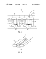
- FIG. 1 shows an embodiment of a circuit in accordance with the present invention.
- FIG. 2 shows an embodiment of conductive elements in accordance with the present invention.
- FIG. 3 shows an embodiment of a tamper detection circuit in accordance with the present invention.
- FIG. 4 shows an embodiment of voltage signals over time when passivation material is present on and between the conductive elements.
- FIG. 5 shows an embodiment of voltage over time when passivation material has been stripped from between and/or around the conductive elements.
- FIG. 1 shows an embodiment 100 of a circuit in accordance with the present invention.
- Embodiment 100 comprises doped regions 110 including doped sub-regions 108 .
- doped regions 110 may be produced using N-type silicon doping and sup-regions 108 , also known as “diffusion regions” within regions 110 , may be created using P-type silicon doping.
- Oxide regions 114 may be formed over portions of regions 110 to act as gates.
- a voltage and/or current signal may be applied to regions 114 to facilitate the exchange of electrons between the regions 108 within a region 110 .
- regions 110 , 114 , and 108 may act as a gate-controlled solid state transistor.
- a voltage and/or current signal may be provided to regions of the solid state transistors by way of vias 104 .
- Vias 104 act to conduct electrical signals between different layers of circuit 100 .
- Circuit 100 may be organized into layers. Each layer may comprise conductive signal paths 102 for routing electrical signals among various elements of the circuit. Signal paths 102 may be encased within a dielectric material 112 , also known as a passivation material or insulator, which protects the signal paths 112 and circuit elements and prevents signals from leaking between various components of the circuit 100 .
- a bonding wire 106 may be coupled to a signal path 102 by way of a via 104 and may conduct signals to and from a terminal of packaging comprising a circuit 100 .
- Circuit 100 may further comprise conductive elements 116 and 118 .
- Elements 116 and 118 may be arranged approximately parallel to certain signal paths 102 of the circuit 1100 .
- FIG. 2 shows an embodiment 200 of conductive elements 116 and 118 in accordance with the present invention. Elements 116 and 118 are arranged proximate to one another and approximately parallel.
- capacitive field 202 may be generated between the elements.
- D is a distance separating facing surfaces of elements 116 and 118 as shown in FIG. 2 .
- the symbol A represents the area of the facing surfaces and may be calculated by multiplying the width W of a facing surface by the length L of the facing surface.
- the value ⁇ 0 is the well known dielectric constant of a vacuum and has an approximate value of 8.854 ⁇ 10 ⁇ 14 F/cm.
- the value ⁇ R is the dielectric constant of the material occupying the space surrounding and between the two elements 116 and 118 .
- passivation material 112 may have ⁇ R of approximately 4, whereas air may have an ⁇ R value of approximately 1.
- the formula demonstrates that the capacitance C produced by the approximately parallel arrangement of conductive elements 116 and 118 is directly proportional to the dielectric constant of the material around and between the elements.
- the capacitive field may extend between and around the circuit elements 116 and 118 , and thus removal of dielectric material 112 from the vicinity (not just between and immediately around) of the elements 116 and 118 may affect the capacitance C.
- FIG. 3 shows an embodiment 300 of a tamper detection circuit in accordance with the present invention.
- Circuit 300 includes two current sources, 302 and 304 .
- current sources 302 and 304 produce substantially identical, constant current through a range of load conditions.
- a reference capacitor 308 is provided which is coupled to current source 304 .
- a voltage at node B will increase approximately linearly due to the application of constant current over time to reference capacitor 308 .
- the rate at which the voltage at node B increases is determined by the capacitance of capacitor 308 .
- a second capacitor 306 is coupled to current source 302 .
- capacitor 306 is defined by conductive elements 116 and 118 .
- a constant current applied to capacitor 306 by source 302 will increase a voltage at node A approximately linearly over time. The rate at which this voltage increases may be determined by the capacitance of capacitor 306 .
- OR gate 310 asserts an enable signal to comparator 312 .
- Comparator 312 may be any device which may compare two input signal values to produce an output signal value indicating if one signal has a value less than the other, or alternately if one signal has a value greater than the other.
- an output signal 314 of comparator 312 is asserted when the voltage on node A exceeds the voltage on node B. Output 314 is not asserted when the voltage level on node B exceeds the voltage level on node A. Asserted output 314 may be used to disable one or more operations of circuit 100 .
- FIG. 4 shows an embodiment of voltage signals over time on nodes A and B when passivation material 112 is present on and between conductive elements 116 and 118 forming capacitor 306 .
- ⁇ R is approximately equal to a value of 4. This affects the capacitance of capacitor 306 in such a fashion that the voltage on node A increases at a slower rate than the voltage on node B.
- OR gate 310 asserts an enable signal to comparator 312 when the voltage at B exceeds logical high. At this point in time and thereafter, the voltage at node B exceeds the voltage at node A and the output of comparator 312 is not asserted. Such a condition indicates that passivation material 112 is present between and around the elements of capacitor 306 .
- FIG. 5 shows an embodiment of voltage over time when passivation material 112 has been stripped from between and/or around the elements 116 and 118 of capacitor 306 .
- OR gate 310 enables comparator 312 .
- Voltage at node A exceeds the voltage at node B which causes comparator to assert its output signal 314 .
- This condition indicates that passivation material 112 has been removed from around and/or between elements 116 and 118 .
- This condition may indicate tampering.
- Signal 314 may be employed to disable one or more circuit operations and thus prevent a party responsible for the tampering from obtaining information about internal operations of the circuit.
- Elements 116 and 118 may be positioned within circuit 100 such that it may be difficult for a party tampering with the circuit 100 to access important internal components without removing passivation material 112 from around or between elements 116 and 118 . Removal of passivation material 112 may result in assertion of tamper detect signal 314 , disabling one or more circuit operations.
- a computer system may comprise a processor and a memory coupled to the processor by way of a bus.
- the memory may store instruction signals which, when executed by the processor, may result in the computer system carrying out certain operations such as reading input signals and producing output signals by way of peripheral devices.
- the processor may encrypt output signals or decrypt input signals from said peripheral devices.
- the present invention may be employed to prevent parties from tampering with the processor circuit to determine characteristics of the encryption or decryption operation.
Landscapes
- Engineering & Computer Science (AREA)
- Computer Hardware Design (AREA)
- Microelectronics & Electronic Packaging (AREA)
- Physics & Mathematics (AREA)
- General Physics & Mathematics (AREA)
- Theoretical Computer Science (AREA)
- Computer Security & Cryptography (AREA)
- Software Systems (AREA)
- General Engineering & Computer Science (AREA)
- Condensed Matter Physics & Semiconductors (AREA)
- Power Engineering (AREA)
- Semiconductor Integrated Circuits (AREA)
Abstract
Description
C=(ε0*εR *A)/D
Here D is a distance separating facing surfaces of
Claims (7)
Priority Applications (1)
| Application Number | Priority Date | Filing Date | Title |
|---|---|---|---|
| US09/466,234 US7024565B1 (en) | 1999-12-17 | 1999-12-17 | Method and apparatus to detect circuit tampering |
Applications Claiming Priority (1)
| Application Number | Priority Date | Filing Date | Title |
|---|---|---|---|
| US09/466,234 US7024565B1 (en) | 1999-12-17 | 1999-12-17 | Method and apparatus to detect circuit tampering |
Publications (1)
| Publication Number | Publication Date |
|---|---|
| US7024565B1 true US7024565B1 (en) | 2006-04-04 |
Family
ID=36102154
Family Applications (1)
| Application Number | Title | Priority Date | Filing Date |
|---|---|---|---|
| US09/466,234 Expired - Fee Related US7024565B1 (en) | 1999-12-17 | 1999-12-17 | Method and apparatus to detect circuit tampering |
Country Status (1)
| Country | Link |
|---|---|
| US (1) | US7024565B1 (en) |
Cited By (16)
| Publication number | Priority date | Publication date | Assignee | Title |
|---|---|---|---|---|
| US20050051351A1 (en) * | 2001-11-28 | 2005-03-10 | De Jongh Petra Elisabeth | Semiconductor device, card, system, and methods of initializing and checking the authenticity and the identify of the semiconductor device |
| US20050216751A1 (en) * | 2004-03-23 | 2005-09-29 | Harris Corporation | Modular cryptographic device providing multi-mode wireless lan operation features and related methods |
| US20100090714A1 (en) * | 2007-01-30 | 2010-04-15 | Nxp, B.V. | Sensing circuit for devices with protective coating |
| US20110095919A1 (en) * | 2008-02-20 | 2011-04-28 | Hypercom Gmbh | Keyboard having capacitance-sensitive key fields |
| US20120062241A1 (en) * | 2010-09-15 | 2012-03-15 | Compagnie Industrielle Et Financiere D'ingenierie "Ingenico" | Device for protecting a connector and a communications wire of a memory card reader |
| US20120062252A1 (en) * | 2010-09-15 | 2012-03-15 | Compagnie Industrielle Et Financiere D'ingenierie "Ingenico" | Protection device, corresponding method and computer software product |
| US20120180140A1 (en) * | 2011-01-06 | 2012-07-12 | Verifone, Inc. | Secure pin entry device |
| EP2056346A3 (en) * | 2007-10-30 | 2012-12-19 | Giesecke & Devrient GmbH | Semi-conductor chip with a protective layer and method of operating a semi-conductor chip |
| US8576536B2 (en) | 2010-09-15 | 2013-11-05 | Compagnie Industrielle et Financiere D'Ingenierie “Ingenico” | Device for protecting an electronic printed circuit board |
| US8903665B2 (en) | 2010-09-15 | 2014-12-02 | Compagnie Industrielle et Financiere D'Ingenierie “Ingenico” | Method and device for protecting an elecronic payment terminal |
| US9021261B2 (en) * | 2007-02-27 | 2015-04-28 | L-3 Communications Corporation | Integrated secure and non-secure display for a handheld communications device |
| CN106997843A (en) * | 2016-01-22 | 2017-08-01 | 中芯国际集成电路制造(上海)有限公司 | Semiconductor devices safety certifying method |
| EP3817000A1 (en) * | 2019-10-29 | 2021-05-05 | Nxp B.V. | Active shielding device and method of active shielding |
| US11044108B1 (en) | 2019-12-24 | 2021-06-22 | CERA Licensing Limited | Temperature sensing physical unclonable function (PUF) authentication system |
| US11107778B2 (en) | 2019-10-29 | 2021-08-31 | Nxp B.V. | Active shielding device and method of active shielding |
| US11516028B2 (en) | 2019-12-24 | 2022-11-29 | CERA Licensing Limited | Temperature sensing physical unclonable function (PUF) authentication system |
Citations (2)
| Publication number | Priority date | Publication date | Assignee | Title |
|---|---|---|---|---|
| US4353056A (en) * | 1980-06-05 | 1982-10-05 | Siemens Corporation | Capacitive fingerprint sensor |
| US5389738A (en) * | 1992-05-04 | 1995-02-14 | Motorola, Inc. | Tamperproof arrangement for an integrated circuit device |
-
1999
- 1999-12-17 US US09/466,234 patent/US7024565B1/en not_active Expired - Fee Related
Patent Citations (2)
| Publication number | Priority date | Publication date | Assignee | Title |
|---|---|---|---|---|
| US4353056A (en) * | 1980-06-05 | 1982-10-05 | Siemens Corporation | Capacitive fingerprint sensor |
| US5389738A (en) * | 1992-05-04 | 1995-02-14 | Motorola, Inc. | Tamperproof arrangement for an integrated circuit device |
Cited By (28)
| Publication number | Priority date | Publication date | Assignee | Title |
|---|---|---|---|---|
| US7525330B2 (en) * | 2001-11-28 | 2009-04-28 | Nxp, B.V. | Semiconductor device, card, system, and methods of initializing and checking the authenticity and the identity of the semiconductor device |
| US20050051351A1 (en) * | 2001-11-28 | 2005-03-10 | De Jongh Petra Elisabeth | Semiconductor device, card, system, and methods of initializing and checking the authenticity and the identify of the semiconductor device |
| US20050216751A1 (en) * | 2004-03-23 | 2005-09-29 | Harris Corporation | Modular cryptographic device providing multi-mode wireless lan operation features and related methods |
| US9003199B2 (en) * | 2004-03-23 | 2015-04-07 | Harris Corporation | Modular cryptographic device providing multi-mode wireless LAN operation features and related methods |
| US20100090714A1 (en) * | 2007-01-30 | 2010-04-15 | Nxp, B.V. | Sensing circuit for devices with protective coating |
| US8138768B2 (en) | 2007-01-30 | 2012-03-20 | Nxp B.V. | Sensing circuit for devices with protective coating |
| US9021261B2 (en) * | 2007-02-27 | 2015-04-28 | L-3 Communications Corporation | Integrated secure and non-secure display for a handheld communications device |
| EP2056346A3 (en) * | 2007-10-30 | 2012-12-19 | Giesecke & Devrient GmbH | Semi-conductor chip with a protective layer and method of operating a semi-conductor chip |
| US20110095919A1 (en) * | 2008-02-20 | 2011-04-28 | Hypercom Gmbh | Keyboard having capacitance-sensitive key fields |
| US8903665B2 (en) | 2010-09-15 | 2014-12-02 | Compagnie Industrielle et Financiere D'Ingenierie “Ingenico” | Method and device for protecting an elecronic payment terminal |
| US8947109B2 (en) * | 2010-09-15 | 2015-02-03 | Compagnie Industrielle et Financiere D'Ingenierie “Ingenico” | Protection device, corresponding method and computer software product |
| US20120062241A1 (en) * | 2010-09-15 | 2012-03-15 | Compagnie Industrielle Et Financiere D'ingenierie "Ingenico" | Device for protecting a connector and a communications wire of a memory card reader |
| US20120062252A1 (en) * | 2010-09-15 | 2012-03-15 | Compagnie Industrielle Et Financiere D'ingenierie "Ingenico" | Protection device, corresponding method and computer software product |
| US8847607B2 (en) * | 2010-09-15 | 2014-09-30 | Compagnie Industrielle et Financiere D'Ingenierie “Ingenico” | Device for protecting a connector and a communications wire of a memory card reader |
| US8576536B2 (en) | 2010-09-15 | 2013-11-05 | Compagnie Industrielle et Financiere D'Ingenierie “Ingenico” | Device for protecting an electronic printed circuit board |
| US20120180140A1 (en) * | 2011-01-06 | 2012-07-12 | Verifone, Inc. | Secure pin entry device |
| US8954750B2 (en) * | 2011-01-06 | 2015-02-10 | Verifone, Inc. | Secure PIN entry device |
| US20140082756A1 (en) * | 2011-01-06 | 2014-03-20 | Verifone, Inc. | Secure pin entry device |
| US8621235B2 (en) * | 2011-01-06 | 2013-12-31 | Verifone, Inc. | Secure pin entry device |
| US9792803B2 (en) | 2011-01-06 | 2017-10-17 | Verifone, Inc. | Secure PIN entry device |
| CN106997843A (en) * | 2016-01-22 | 2017-08-01 | 中芯国际集成电路制造(上海)有限公司 | Semiconductor devices safety certifying method |
| CN106997843B (en) * | 2016-01-22 | 2020-05-01 | 中芯国际集成电路制造(上海)有限公司 | Semiconductor device safety authentication method |
| EP3817000A1 (en) * | 2019-10-29 | 2021-05-05 | Nxp B.V. | Active shielding device and method of active shielding |
| US11107778B2 (en) | 2019-10-29 | 2021-08-31 | Nxp B.V. | Active shielding device and method of active shielding |
| US11436383B2 (en) | 2019-10-29 | 2022-09-06 | Nxp B.V. | Active shielding device and method of active shielding |
| US11044108B1 (en) | 2019-12-24 | 2021-06-22 | CERA Licensing Limited | Temperature sensing physical unclonable function (PUF) authentication system |
| US11516028B2 (en) | 2019-12-24 | 2022-11-29 | CERA Licensing Limited | Temperature sensing physical unclonable function (PUF) authentication system |
| US11652649B2 (en) | 2019-12-24 | 2023-05-16 | CERA Licensing Limited | Sensor secured by physical unclonable function (PUF) |
Similar Documents
| Publication | Publication Date | Title |
|---|---|---|
| US7024565B1 (en) | Method and apparatus to detect circuit tampering | |
| US9121896B2 (en) | Device for detecting the thinning down of the substrate of an integrated circuit chip | |
| US20140042442A1 (en) | Reliable physical unclonable function for device authentication | |
| US8946859B2 (en) | Device for detecting an attack in an integrated circuit chip | |
| US8511567B2 (en) | Smart card chip arrangement | |
| US4814849A (en) | Monolithically integrated semiconductor circuit | |
| US20110234307A1 (en) | Countermeasure method and device against an attack by fault injection in an electronic microcircuit | |
| US9991892B2 (en) | Electronic device having a physical unclonable function identifier | |
| US20130320491A1 (en) | Semiconductor Device Having Features to Prevent Reverse Engineering | |
| EP3249417B1 (en) | Sensing and detection of esd and other transient overstress events | |
| CA2897486A1 (en) | Semiconductor device having features to prevent reverse engineering | |
| JP2001244414A (en) | Semiconductor integrated circuit | |
| US11531049B2 (en) | Electromagnetic pulse detection | |
| US4288694A (en) | High-impedance IGFET input circuit suitable for smoke detector I.C. | |
| JP3048429B2 (en) | Semiconductor integrated circuit device | |
| JP4759085B2 (en) | Component with integrated circuit having crypto processor and method of installing the same | |
| JP4393707B2 (en) | Data carrier having data processing means and current peak pattern suppressing means | |
| US11270957B2 (en) | Method for detecting a breach of the integrity of a semiconductor substrate of an integrated circuit from its rear face, and corresponding device | |
| US20170092599A1 (en) | Semiconductor Device Having Features to Prevent Reverse Engineering | |
| US20120268160A1 (en) | Implementing temporary disable function of protected circuitry by modulating threshold voltage of timing sensitive circuit | |
| Beckmeier et al. | Variation-resilient quantifiable plasma process induced damage monitoring | |
| JP2000076140A (en) | Semiconductor integrated circuit | |
| JP3728389B2 (en) | Semiconductor chip with surface cover | |
| Abedi et al. | High-precision nano-amp current sensor and obfuscation based analog trojan detection circuit | |
| JP2008311285A (en) | Semiconductor device, and test circuit and evaluation method using same |
Legal Events
| Date | Code | Title | Description |
|---|---|---|---|
| AS | Assignment |
Owner name: INTEL CORPORATION, CALIFORNIA Free format text: ;ASSIGNORS:BEILEY, MARK A.;BREISCH, JAMES E.;REEL/FRAME:010647/0063 Effective date: 20000218 |
|
| AS | Assignment |
Owner name: INTEL CORPORATION, CALIFORNIA Free format text: ASSIGNMENT/DOCUMENT PREVIOUSLY RECORDED AT REEL/FRAME 10647/0063 CONTAINED ERRORS IN PROPERTY NUMBERS 09466246. DOCUMENT RE-RECORDED TO CORRECT ERRORS ON STATED REEL.;ASSIGNORS:BEILEY, MARK A.;BREISCH, JAMES E.;REEL/FRAME:010781/0270 Effective date: 20000615 |
|
| FPAY | Fee payment |
Year of fee payment: 4 |
|
| FPAY | Fee payment |
Year of fee payment: 8 |
|
| FEPP | Fee payment procedure |
Free format text: MAINTENANCE FEE REMINDER MAILED (ORIGINAL EVENT CODE: REM.) |
|
| LAPS | Lapse for failure to pay maintenance fees |
Free format text: PATENT EXPIRED FOR FAILURE TO PAY MAINTENANCE FEES (ORIGINAL EVENT CODE: EXP.) |
|
| STCH | Information on status: patent discontinuation |
Free format text: PATENT EXPIRED DUE TO NONPAYMENT OF MAINTENANCE FEES UNDER 37 CFR 1.362 |
|
| FP | Lapsed due to failure to pay maintenance fee |
Effective date: 20180404 |