US7031894B2 - Generating a library of simulated-diffraction signals and hypothetical profiles of periodic gratings - Google Patents
Generating a library of simulated-diffraction signals and hypothetical profiles of periodic gratings Download PDFInfo
- Publication number
- US7031894B2 US7031894B2 US10/051,830 US5183002A US7031894B2 US 7031894 B2 US7031894 B2 US 7031894B2 US 5183002 A US5183002 A US 5183002A US 7031894 B2 US7031894 B2 US 7031894B2
- Authority
- US
- United States
- Prior art keywords
- hypothetical
- diffraction
- layers
- profile
- simulated
- Prior art date
- Legal status (The legal status is an assumption and is not a legal conclusion. Google has not performed a legal analysis and makes no representation as to the accuracy of the status listed.)
- Active, expires
Links
Images


Classifications
-
- G—PHYSICS
- G01—MEASURING; TESTING
- G01N—INVESTIGATING OR ANALYSING MATERIALS BY DETERMINING THEIR CHEMICAL OR PHYSICAL PROPERTIES
- G01N21/00—Investigating or analysing materials by the use of optical means, i.e. using sub-millimetre waves, infrared, visible or ultraviolet light
- G01N21/84—Systems specially adapted for particular applications
- G01N21/88—Investigating the presence of flaws or contamination
- G01N21/95—Investigating the presence of flaws or contamination characterised by the material or shape of the object to be examined
- G01N21/956—Inspecting patterns on the surface of objects
-
- G—PHYSICS
- G01—MEASURING; TESTING
- G01B—MEASURING LENGTH, THICKNESS OR SIMILAR LINEAR DIMENSIONS; MEASURING ANGLES; MEASURING AREAS; MEASURING IRREGULARITIES OF SURFACES OR CONTOURS
- G01B11/00—Measuring arrangements characterised by the use of optical techniques
-
- G—PHYSICS
- G01—MEASURING; TESTING
- G01N—INVESTIGATING OR ANALYSING MATERIALS BY DETERMINING THEIR CHEMICAL OR PHYSICAL PROPERTIES
- G01N21/00—Investigating or analysing materials by the use of optical means, i.e. using sub-millimetre waves, infrared, visible or ultraviolet light
- G01N21/17—Systems in which incident light is modified in accordance with the properties of the material investigated
- G01N21/47—Scattering, i.e. diffuse reflection
- G01N21/4788—Diffraction
Definitions
- the present invention relates to wafer metrology, and more particularly to generating a library of simulated-diffraction signals for use in optical metrology to determine the profile of periodic gratings.
- periodic gratings are typically utilized for quality assurance.
- one typical use of such periodic gratings includes fabricating a periodic grating in proximity to the operating structure of a semiconductor chip. By determining the profile of the periodic grating, the quality of the fabrication process utilized to form the periodic grating, and by extension the semiconductor chip proximate the periodic grating, can be evaluated.
- Optical metrology can be utilized to determine the profile of a periodic grating.
- optical metrology involves directing an incident beam at the periodic grating, and measuring the resulting diffraction beam.
- the characteristics of the measured-diffraction beam i.e., a measured-diffraction signal
- a library of pre-determined diffraction signals i.e., hypothetical-diffraction signals
- the profile associated with the matching hypothetical-diffraction signal is presumed to represent the profile of the periodic grating.
- the process of generating a hypothetical-diffraction signal involves performing a large number of complex calculations, which can be time and computationally intensive.
- the amount of time and computational capability and capacity needed to generate hypothetical-diffraction signals can limit the size and resolution (i.e., the number of entries and the increment between entries) of the library of hypothetical-diffraction signals that can be generated.
- a library of simulated-diffraction signals and hypothetical profiles of a periodic grating is generated by generating diffraction calculations for a plurality of blocks of hypothetical layers.
- a diffraction calculation for a block of hypothetical layers characterizes, in part, the behavior of a diffraction beam in the block of hypothetical layers.
- Each block of hypothetical layers includes two or more hypothetical layers, and each hypothetical layer characterizes a layer within a hypothetical profile.
- the diffraction calculations for the blocks of hypothetical layers are stored prior to generating the library.
- the simulated-diffraction signals to be stored in the library are then generated based on the stored diffraction calculations for the blocks of hypothetical layers.
- FIG. 1 depicts an exemplary optical-metrology system.
- FIG. 2 depicts another exemplary optical-metrology system.
- FIGS. 3A–3E depict various hypothetical profiles of periodic gratings.
- FIG. 4 depicts an exemplary cache and library.
- FIGS. 5A and 5B depict an exemplary process of generating simulated-diffraction signals.
- FIGS. 6A and 6B depict another exemplary process of generating simulated-diffraction signals.
- FIGS. 7A and 7B depict still another exemplary process of generating simulated-diffraction signals.
- FIG. 8 depicts an exemplary computer system.
- FIG. 9 shows a section of a periodic grating.
- FIGS. 10A–10C depict cross sectional views of a portion of a periodic grating.
- FIG. 11 depicts an exemplary coupled-wave analysis.
- FIG. 12 depicts another exemplary coupled-wave analysis.
- FIG. 13 depicts an exemplary process of generating simulated-diffraction signals.
- FIG. 14 depicts another exemplary process of generating simulated-diffraction signals.
- FIG. 15 is another exemplary computer system.
- FIGS. 16A–16D depict exemplary ridge profiles.
- FIG. 17 depicts an exemplary aggregate-layer trapezoid.
- FIG. 18 depicts an exemplary process of generating a library of simulated-diffraction signals.
- a periodic grating 145 is depicted on a semiconductor wafer 140 .
- wafer 140 is disposed on a process plate 180 , which can include a chill plate, a hot plate, a developer module, and the like.
- wafer 140 can also be disposed on a wafer track, in the end chamber of an etcher, in an end-station or metrology station, in a chemical mechanical polishing tool, and the like.
- periodic grating 145 can be formed in test areas on wafer 140 that are proximate to or within an operating structure formed on wafer 140 .
- periodic grating 145 can be formed adjacent to a device formed on wafer 140 .
- periodic grating 145 can be formed in an area of the device that does not interfere with the operation of the device.
- the profile of periodic grating 145 is obtained to determine whether periodic grating 145 , and by extension the operating structure adjacent periodic grating 145 , has been fabricated according to specifications.
- optical-metrology can be utilized to obtain the profile of periodic grating 145 .
- an optical-metrology system 100 can include an electromagnetic source 120 , such as an ellipsometer, reflectometer, and the like.
- Periodic grating 145 is illuminated by an incident beam 110 from electromagnetic source 120 .
- Incident beam 110 is directed onto periodic grating 145 at an angle of incidence ⁇ i with respect to normal ⁇ right arrow over (n) ⁇ of periodic grating 145 .
- Diffraction beam 115 leaves at an angle of ⁇ d with respect to normal ⁇ right arrow over (n) ⁇ .
- the angle of incidence ⁇ i is near the Brewster's angle.
- the angle of incidence ⁇ i can vary depending on the application.
- the angle of incidence ⁇ i is between about 0 and about 40 degrees.
- the angle of incidence ⁇ i is between about 30 and about 90 degrees.
- the angle of incidence ⁇ i is between about 40 and about 75 degrees.
- the angle of incidence ⁇ i is between about 50 and about 70 degrees.
- Electromagnetic source 120 can include focusing optics to control the spot size of incident beam 110 .
- spot size of incident beam 110 can be reduced to less than the size of the test area on wafer 140 that contains periodic grating 145 .
- a spot size of about 50 ⁇ m by 50 ⁇ m, or smaller, can be used.
- electromagnetic source 120 can include a pattern recognition module to center the spot in the test area on wafer 140 .
- diffraction beam 115 is received by detector 170 .
- electromagnetic source 120 is an ellipsometer
- the magnitude ( ⁇ ) and the phase ( ⁇ ) of diffraction beam 115 are received and detected.
- electromagnetic source 120 is a reflectometer
- the relative intensity of diffraction beam 115 is received and detected.
- optical-metrology system 100 includes a processing module 190 , which converts diffraction beam 115 received by detector 170 into a diffraction signal (i.e., a measured-diffraction signal). Processing module 190 then compares the measured-diffraction signal to the simulated-diffraction signals stored in a library 185 . As will be described in greater detail below, each simulated-diffraction signal in library 185 is associated with a theoretical profile. When a match is made between the measured-diffraction signal and one of the simulated-diffraction signals in library 185 , the theoretical profile associated with the matching simulated-diffraction signal is presumed to represent the actual profile of periodic grating 145 . The matching simulated-diffraction signal and/or theoretical profile can then be utilized to determine whether the periodic grating has been fabricated according to specifications.
- a processing module 190 converts diffraction beam 115 received by detector 170 into a diffraction signal (i.e., a measured-diffraction
- optical-metrology system 100 has been described and depicted thus far as having a single electromagnetic source 120 and a single detector 170 , it should be recognized that optical-metrology system 100 can include any number of electromagnetic sources 120 and detectors 170 .
- optical-metrology system 100 is depicted with two electromagnetic sources 120 A and 120 B, and two detectors 170 A and 170 B.
- Two incident beams 110 A and 110 B are generated by electromagnetic sources 120 A and 120 B, with each incident beam 110 A and 110 B including two polarizations of the electromagnetic wave to allow for both intensity and phase measurements.
- an optical fiber 125 can transport broadband radiation from a source (not shown) to the electromagnetic sources 120 A and 120 B.
- a switching mechanism 200 can direct the broadband radiation alternately to the two optic fiber branches 125 A and 125 B, which lead to the electromagnetic sources 120 A and 120 B, respectively.
- the switching mechanism 200 is a wheel with an opening in one semicircle, so that rotation of the switching wheel 200 by 180 degrees produces a switching of the optic fiber branch 125 A or 125 B to which the radiation is directed.
- the incident beams are directed to wafer 140 so that the angles of incidence ⁇ i1 and ⁇ i2 are approximately 50 and 70 degrees.
- incidence ⁇ i1 and ⁇ i2 are chosen to be disparate enough that redundancy of information is not an issue, while both ⁇ i1 and ⁇ i2 are chosen to be close enough to Brewster's angle that the incident beam is sensitive to the grating features.
- diffraction beams 115 A and 115 B leave the wafer at angles ⁇ d1 and ⁇ d2 .
- Diffraction beams 115 A and 115 B are then received by detectors 170 A and 170 B.
- electromagnetic sources 120 A and 120 B are ellipsometers, the magnitude ( ⁇ ) and the phase ( ⁇ ) of diffraction beams 115 A and 115 B are received and detected.
- electromagnetic source 120 is a reflectometer, the relative intensity of diffraction beams 115 A and 115 B is received and detected.
- multiple detectors 170 A and 170 B are not necessary to perform multiple-angle reflectometry or ellipsometry measurements. Instead, a single electromagnetic source 120 and detector 170 can perform a first measurement for an angle of incidence of ⁇ i1 , and then be moved to perform a second measurement for an angle of incidence of ⁇ i2 .
- library 185 includes simulated-diffraction signals that are associated with theoretical profiles of periodic grating 145 . More particularly, in one exemplary embodiment, library 185 includes pairings of simulated-diffraction signals and theoretical profiles of periodic grating 145 .
- the simulated-diffraction signal in each pairing includes theoretically generated reflectances that characterize the predicted behavior of diffraction beam 115 assuming that the profile of the periodic grating 145 is that of the theoretical profile in the simulated-diffraction signal and theoretical profile pairing.
- the set of hypothetical profiles stored in library 185 can be generated by characterizing a hypothetical profile using a set of parameters, then varying the set of parameters to generate hypothetical profiles of varying shapes and dimensions.
- the process of characterizing a profile using a set of parameters can also be referred to as parameterizing.
- hypothetical profile 300 can be characterized by parameters h 1 and w 1 that define its height and width, respectively.
- additional shapes and features of hypothetical profile 300 can be characterized by increasing the number of parameters.
- hypothetical profile 300 can be characterized by parameters h 1 , w 1 , and w 2 that define its height, bottom width, and top width, respectively.
- the width of hypothetical profile 300 can be referred to as the critical dimension (CD).
- parameter w 1 and w 2 can be described as defining the bottom CD and top CD, respectively, of hypothetical profile 300 .
- the set of hypothetical profiles stored in library 185 can be generated by varying the parameters that characterize the hypothetical profile. For example, with reference to FIG. 3B , by varying parameters h 1 , w 1 , and w 2 , hypothetical profiles of varying shapes and dimensions can be generated. Note that one, two, or all three parameters can be varied relative to one another.
- the number of hypothetical profiles in the set of hypothetical profiles stored in library 185 depends, in part, on the range over which the set of parameters and the increment at which the set of parameters are varied.
- the range and increment can be selected based on familiarity with the fabrication process for periodic grating 145 and what the range of variance is likely to be.
- the range and increment can also be selected based on empirical measures, such as measurements using AFM, X-SEM, and the like.
- the simulated-diffraction signals stored in library 185 can be generated by generating a simulated-diffraction signal for each hypothetical profile in the set of hypothetical profiles stored in library 185 .
- the process of generating a simulated-diffraction signal can involve performing a large number of complex calculations. Additionally, as the complexity of the theoretical profile increases, so does the number and complexity of the calculations needed to generate the simulated-diffraction signal for the theoretical profile. Furthermore, as the number of theoretical profiles increases, so does the amount of time and processing capacity and capability needed to generate library 185 .
- a portion of the calculations performed in generating simulated-diffraction signals can be stored as intermediate calculations prior to generating library 185 .
- the simulated-diffraction signals for each hypothetical profile in library 185 can then be generated using these intermediate calculations rather than performing all of the calculations needed to generate a simulated-diffraction signal for each theoretical profile in library 185 .
- diffraction calculations are generated for a plurality of blocks of hypothetical layers.
- a diffraction calculation for a block of hypothetical layers characterizes, in part, the behavior of diffraction beam 115 in the block of hypothetical layers.
- Each block of hypothetical layers includes two or more hypothetical layers, and each hypothetical layer characterizes a layer within a hypothetical profile.
- the diffraction calculations for the blocks of hypothetical layers are stored prior to generating library 185 .
- the simulated-diffraction signals to be stored in library 185 are generated based on the stored diffraction calculations for the blocks of hypothetical layers.
- a plurality of hypothetical layers 402 can be grouped together as a block of hypothetical layers 404 (e.g., block of hypothetical layers 404 . 1 – 404 . 4 ).
- Each hypothetical layer 402 characterizes a layer of a hypothetical profile.
- hypothetical layers 402 . 1 , 402 . 2 , and 402 . 3 are depicted as being grouped together to form block of hypothetical layers 404 . 1 .
- Hypothetical layers 402 . 4 , 402 . 5 , and 402 . 6 are depicted as being grouped together to form block of hypothetical layers 404 . 2 .
- Hypothetical layers 402 . 7 , 402 . 8 , and 402 . 9 are depicted as being grouped together to form block of hypothetical layers 404 . 3 .
- Hypothetical layers 402 . 10 , 402 . 11 , and 402 . 12 are depicted as being grouped together to form block of hypothetical layers 404 . 4 .
- blocks of hypothetical layers 404 of various sizes and shapes can be generated. Although blocks of hypothetical layers 404 are depicted in FIG. 4 as including three hypothetical layers 402 , it should be recognized that they can include any number of hypothetical layers 402 .
- Diffraction calculations which characterize the behavior of diffraction signals, are generated for each hypothetical layer 402 within a block of hypothetical layers 404 .
- Diffraction calculations for each block of hypothetical layers 404 are then generated by aggregating the diffraction calculations for each hypothetical layer 402 within each block of hypothetical layers 404 .
- the diffraction calculations and the blocks of hypothetical layers 404 are then stored. More particularly, in one exemplary embodiment, pairs of diffraction calculations and blocks of hypothetical layers 404 are stored in a cache 406 .
- diffraction calculations are generated for hypothetical layers 402 . 1 , 402 . 2 , and 402 . 3 .
- a diffraction calculation for block of hypothetical layers 404 . 1 is then generated by aggregating diffraction calculations for hypothetical layers 402 . 1 , 402 . 2 , and 402 . 3 .
- Block of hypothetical layers 404 . 1 and the diffraction calculations associated with block of hypothetical layers 404 . 1 are then stored in cache 406 .
- diffraction calculations for blocks of hypothetical layers 404 . 2 , 404 . 3 , and 404 . 4 are generated and stored in cache 406 .
- cache 406 may contain tens and hundreds of thousands of blocks of hypothetical layers 404 and diffraction calculations.
- FIG. 4 depicts blocks of hypothetical layers 404 being stored in cache 406 in a graphical format
- blocks of hypothetical layers 404 can be stored in various formats.
- blocks of hypothetical layers 404 can be stored using parameters that define their shapes.
- simulated-diffraction signals for a set of hypothetical profiles to be stored in library 185 can be generated based on the diffraction calculations for blocks of hypothetical layers 404 stored in cache 406 . More particularly, for each hypothetical profile to be stored in library 185 , one or more blocks of hypothetical layers 404 that characterize the hypothetical profile are selected from those stored in cache 406 . Boundary conditions are then applied to generate the simulated-diffraction signal for the hypothetical profile. The simulated-diffraction signal and the hypothetical profile are then stored in library 185 .
- the hypothetical profile can be stored in various formats, such as graphically, using the parameters that define the hypothetical profile, or both.
- one block of hypothetical layers 404 can be used to characterize a hypothetical profile. For example, with reference to FIG. 5A , assume for the sake of this example that a simulated-diffraction signal is to be generated for hypothetical profile 300 A. As described above, a block of hypothetical layers 404 from cache 406 is selected that characterizes hypothetical profile 300 A. The appropriate block of hypothetical layers 404 can be selected using an error minimization algorithm, such as a sum-of-squares algorithm.
- block of hypothetical layers 404 . 1 is selected from cache 406 .
- the diffraction calculation associated with block of hypothetical layers 404 . 1 is then retrieved from cache 406 .
- Boundary conditions are then applied to generate the simulated-diffraction signal for hypothetical profile 300 A.
- the simulated-diffraction signal and hypothetical profile 300 A are then stored in library 185 .
- the parameters that define hypothetical profile 300 A can be varied to define another hypothetical profile.
- the parameters are varied to define hypothetical profile 300 B.
- block of hypothetical layers 404 . 4 is selected from cache 406 .
- the diffraction calculation associated with block of hypothetical layers 404 . 4 is then retrieved from cache 406 .
- Boundary conditions are then applied to generate the simulated-diffraction signal for hypothetical profile 300 B.
- the simulated-diffraction signal and hypothetical profile 300 B are then stored in library 185 .
- any number of hypothetical profiles and simulated-diffraction signals can be generated and stored in library 185 using blocks of hypothetical layers 404 and the diffraction calculations in cache 406 .
- blocks of hypothetical layers 404 and the diffraction calculations in cache 406 are generated before generating library 185 .
- the calculations needed to generate the diffraction calculations associated with blocks of hypothetical layers 404 do not need to be performed at the time that library 185 is generated. This can have the advantage that the amount of time and calculations needed to generate library 185 can be reduced.
- multiple blocks of hypothetical layers 404 can be used to characterize a hypothetical profile.
- profile 300 A can be characterized by blocks of hypothetical layers 404 . 1 , 404 . 2 , and 404 . 3 .
- an error minimization algorithm can be utilized to determine the appropriate blocks of hypothetical layers 404 to use in characterizing profile 300 A.
- profile 300 A the diffraction calculations associated with blocks of hypothetical layers 404 . 1 , 404 . 2 , and 404 . 3 are retrieved from cache 406 . Boundary conditions are then applied to generate the simulated-diffraction signal for profile 300 A. More particularly, the boundary conditions at the top and bottom of profile 300 A are applied. The resulting simulated-diffraction signal and profile 300 A are then stored in library 185 .
- the parameters that define hypothetical profile 300 A can be varied to define another profile.
- the parameters are varied to define hypothetical profile 300 B.
- hypothetical profile 300 B can be characterized by blocks of hypothetical layers 404 . 1 , 404 . 3 , and 404 . 4 .
- the diffraction calculations associated with blocks of hypothetical layers 404 . 1 , 404 . 3 , and 404 . 4 are retrieved from cache 406 .
- Boundary conditions are then applied to generate the simulated-diffraction signal for hypothetical profile 300 B.
- the resulting simulated-diffraction signal and hypothetical profile 300 B are then stored in library 185 .
- a hypothetical profile can include multiple materials.
- hypothetical profile 300 is used to characterize an actual profile of a grating periodic formed from two materials. More particularly, as depicted in FIG. 7A , hypothetical profile 300 includes a first layer 702 and a second layer 704 .
- first layer 702 represents an oxide layer of the actual profile
- second layer 704 represents a metal layer of the actual profile.
- hypothetical profile 300 can include any number of layers to represent layers of any number of materials in an actual profile.
- cache 406 includes blocks of hypothetical layers 404 of various materials as well as various shapes.
- blocks of hypothetical profiles 404 . 1 and 404 . 3 represent oxide layers
- hypothetical profiles 404 . 2 and 404 . 4 represent metal layers.
- profile 300 can be characterized by blocks of hypothetical layers 404 . 3 and 404 . 4 from cache 406 . Boundary conditions are then applied to generate the simulated-diffraction signal for profile 300 .
- the simulated-diffraction signal and profile 300 are then stored in library 185 .
- hypothetical layers 402 and blocks of hypothetical layers 404 have been depicted as having rectangular and trapezoidal shapes, respectively.
- the diffraction calculation for a hypothetical layer 402 depends on its width but not on its height.
- the diffraction calculation for a block of hypothetical layers 404 depends on its height as well as its width. Therefore, the blocks of hypothetical layers 404 stored in cache 406 are characterized and indexed, in part, by their width and their height. More particularly, when blocks of hypothetical layers 404 have symmetric-trapezoidal shapes, they can be indexed by their height, bottom width (bottom CD), and top width (top CD).
- blocks of hypothetical layers 404 can have various shapes. As such, they can be characterized and indexed using any number of parameters.
- library 185 can be generated using computer system 800 .
- the process of generating library 185 can involve performing a large number of complex calculations.
- a set of hypothetical profiles is to be generated for a periodic grating that is to have a profile with a bottom CD of 200 nm.
- a 10% process variation is expected for the bottom CD of the periodic grating, which means that the bottom CD is expected to vary between about 180 to about 220 nm.
- the top CD is expected to vary between about 160 to about 180 nm.
- the nominal thickness (i.e., the height) of the periodic grating is to be about 500 nm, and that a 10% process variation is expected, which means that the height can vary between about 450 to about 550 nm.
- the desired resolution is 1 nm, which means that each parameter of the hypothetical profiles is varied by an increment of 1 nm.
- the top CD of the hypothetical profiles is varied between 160 to 180 nm in steps of 1 nm.
- the bottom CD of the hypothetical profiles is varied between 180 to 220 nm in steps of 1 nm.
- the thickness/height of the hypothetical profiles is varied between 450 to 550 nm in steps of 1 nm.
- each diffraction calculation uses 6 matrices with 9 orders and 8 bytes, which totals 17 kbytes. As such, in this example, to store the diffraction calculations for all of the 87,000 hypothetical profiles at 53 different wavelengths, a total of 78 Gigabytes is needed.
- computer system 800 can include multiple processors 802 configured to perform portions of the computations in parallel.
- computer system 800 can be configured with a single processor 802 .
- computer system 800 can include a memory 804 configured with a large amount of memory, such as 8 Gigabytes, 16 Gigabytes, 32 Gigabytes, and the like, that can be accessed by the multiple processors 802 . It should be recognized, however, computer system 800 can be configured with any number and size of memories 804 .
- cache 406 can reside in memory 804 .
- the blocks of hypothetical layers and hypothetical profiles stored in cache 406 can be more quickly accessed by computer system 800 , and more particularly processors 802 , than if cache 406 resided on a hard drive.
- library 185 can reside on various computer-readable storage media.
- library 185 can reside on a compact disk that is written to by computer system 800 when library 185 is generated, and read by signal processing module 190 ( FIG. 1 ) when library 185 is used to determine the profile of periodic grating 145 ( FIG. 1 ) on wafer 140 ( FIG. 1 ).
- simulated-diffraction signals are generated for hypothetical profiles based on diffraction calculation generated for hypothetical layers 402 and blocks of hypothetical layers 404 .
- simulated-diffraction signals and diffraction calculations can be generated by applying Maxwell's equations and using a numerical analysis technique to solve Maxwell's equations. More particularly, in the exemplary embodiment described below, rigorous coupled-wave analysis is used. It should be noted, however, that various numerical analysis techniques, including variations of the rigorous coupled-wave analysis technique described below, can be used.
- a section of periodic grating 145 is shown.
- the section of the grating 145 is depicted as having three ridges 902 , which have a triangular cross-section.
- ridges can have shapes that are considerably more complex, and the categories of “ridges” and “troughs” may be ill-defined.
- the term “ridge” will be used hereafter to refer to one period of a periodic structure on a substrate.
- Each ridge 902 is considered to extend infinitely in the +y and ⁇ y directions, and an infinite, regularly-spaced series of such ridges 902 are considered to extend in the +x and ⁇ x directions.
- the ridges 902 are atop a deposited film 904 , and the film 904 is atop a substrate 906 , which is considered to extend semi-infinitely in the +z direction.
- the normal vector n to the grating is in the ⁇ z direction.
- FIG. 9 illustrates the variables associated with a mathematical analysis of a diffraction grating according to the present exemplary embodiment.
- FIG. 9 illustrates the variables associated with a mathematical analysis of a diffraction grating according to the present exemplary embodiment.
- FIG. 10A shows a cross-sectional view of two ridges 902 of periodic grating 145 illustrating the variables associated with a mathematical description of the dimensions of the diffraction grating 145 .
- FIG. 10A shows a cross-sectional view of two ridges 902 of periodic grating 145 illustrating the variables associated with a mathematical description of the dimensions of the diffraction grating 145 .
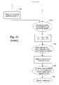
- a Fourier space version of Maxwell's equations is used. As shown in the calculation process flow diagram of FIG. 11 , the permittivities ⁇ l (x) for each layer l are determined or acquired ( 1110 ), and a one-dimensional Fourier transformation of the permittivity ⁇ l (x) of each layer l is performed ( 1112 ) along the direction of periodicity, ⁇ circumflex over (x) ⁇ , of the periodic grating 145 to provide the harmonic components of the permittivity ⁇ l,i , where i is the order of the harmonic component.
- ⁇ l , 0 n r 2 ⁇ d l D + n 0 2 ⁇ ( 1 - d l D ) , ( 1.1 ⁇ .2 ) and for i not equal to zero,
- n r is the index of refraction of the material in the ridges 902 in layer l
- the index of refraction n o of the atmospheric layer 1002 is typically near unity
- the present specification explicitly addresses periodic gratings where a single ridge material and a single atmospheric material are found along any line in the x-direction. However, gratings can have more than one ridge material along a line in the
- E l [ ⁇ l , 0 ⁇ l , - 1 ⁇ l , - 2 ⁇ ⁇ l , - 2 ⁇ o ⁇ l , 1 ⁇ l , 0 ⁇ l , - 1 ⁇ ⁇ l , - ( 2 ⁇ o - 1 ) ⁇ l , 2 ⁇ l , 1 ⁇ l , 0 ⁇ ⁇ l , - ( 2 ⁇ o - 2 ) ⁇ ⁇ ⁇ ⁇ ⁇ l , 2 ⁇ o ⁇ l , ( 2 ⁇ o - 1 ) ⁇ l , ( 2 ⁇ o - 2 ) ⁇ ⁇ l , 0 ] . ( 1.1 ⁇ .4 )
- the x-components k xi of the outgoing wave vectors satisfy the Floquet condition (which is also called Bloch's Theorem, see Solid State Physics, N. W. Ashcroft and N. D. Mermin, Saunders College, Philadelphia, 1976, pages 133–134) in each of the layers 1025 containing the periodic ridges 902 , and therefore, due to the boundary conditions, in the atmospheric layer 1002 and the substrate layer 906 as well. That is, for a system having an n-dimensional periodicity given by
- ⁇ right arrow over (d) ⁇ i are the basis vectors of the periodic system, and m i takes on positive and negative integer values, the Floquet condition requires that the wave vectors ⁇ right arrow over (k) ⁇ satisfy
- ⁇ right arrow over (k) ⁇ 0 is the wave vector of a free-space solution
- ⁇ ij the Kronecker delta function.
- the layers 1025 of the periodic grating 145 of FIGS. 9 and 10 which have the single reciprocal lattice vector ⁇ right arrow over (b) ⁇ is ⁇ circumflex over (x) ⁇ /D, thereby providing the relationship of equation (1.2.3).
- the formulation given above for the electric field in the atmospheric layer 1002 although it is an expansion in terms of plane waves, is not determined via a Fourier transform of a real-space formulation. Rather, the formulation is produced ( 1124 ) a priori based on the Floquet condition and the requirements that both the incoming and outgoing radiation have wave vectors of magnitude n 0 k 0 . Similarly, the plane wave expansion for the electric field in the substrate layer 906 is produced ( 1124 ) a priori.
- the electric field ⁇ right arrow over (E) ⁇ is formulated ( 1124 ) as a transmitted wave which is a sum of plane waves where the x-components k xi of the wave vectors (k xi , k 0,zi ) satisfy the Floquet condition, i.e.,
- the plane wave expansions for the electric and magnetic fields in the intermediate layers 1025 . 1 through 1025 .(L ⁇ 1) are also produced ( 1134 ) a priori based on the Floquet condition.
- the electric field ⁇ right arrow over (E) ⁇ l,y in the lth layer is formulated ( 1134 ) as a plane wave expansion along the direction of periodicity, ⁇ circumflex over (x) ⁇ , i.e.,
- equation (1.3 ⁇ .5 ) While equation (1.3.3) only couples harmonic amplitudes of the same order i, equation (1.3.5) couples harmonic amplitudes S l and U l between harmonic orders. In equation (1.3.5), permittivity harmonics ⁇ i from order ⁇ 2o to +2o are required to couple harmonic amplitudes S l and U l of orders between ⁇ o and +o.
- [K x ] is a diagonal matrix with the (i,i) element being equal to (k xi /k 0 )
- the permittivity harmonics matrix [E l ] is defined above in equation (1.1.4)
- [S l,y ] and [ ⁇ 2 S l,y / ⁇ z, 2 ] are column vectors with indices i running from ⁇ o to +o, i.e.,
- [ S l , y ] [ S l , y , ( - o ) ⁇ S l , y , 0 ⁇ S l , y , o ] , ( 1.3.8 )
- a diagonal root-eigenvalue matrix [Q l ] is defined to be diagonal entries q l,i which are the positive real portion of the square roots of the eigenvalues ⁇ l,i .
- the coefficients c 1 and c 2 are, as yet, undetermined.
- the coefficients c 1 and c 2 in the homogeneous solutions of equations (1.3.9) and (1.3.11) are determined by applying ( 1155 ) the requirement that the tangential electric and magnetic fields be continuous at the boundary between each pair of adjacent layers 1025 .l/( 1025 .(l+1). At the boundary between the atmospheric layer 1002 and the first layer 1025 . 1 , continuity of the electric field E y and the magnetic field H x requires
- the top half of matrix equation (1.4.1) provides matching of the electric field E y across the boundary of the atmospheric layer 1025 . 0 and the first layer 1025 . 1
- the bottom half of matrix equation (1.4.1) provides matching of the magnetic field H x across the layer boundary 1025 . 0 / 1025 . 1
- the vector on the far left is the contribution from the incoming radiation 910 in the atmospheric layer 1002
- the second vector on the left is the contribution from the reflected radiation 914 in the atmospheric layer 1002
- the portion on the right represents the fields E y and H x in the first layer 1025 . 1 .
- the method ( 1200 ) of calculation for the diffracted reflectivity of TM-polarized incident electromagnetic radiation 910 shown in FIG. 12 parallels the method ( 1100 ) described above and shown in FIG. 11 for the diffracted reflectivity of TE-polarized incident electromagnetic radiation 910 .
- the variables describing the geometry of the grating 145 and the geometry of the incident radiation 910 are as shown in FIGS. 9 and 10A .
- the electric field vector ⁇ right arrow over (E) ⁇ is in the plane of incidence 912
- the magnetic field vector ⁇ right arrow over (H) ⁇ is perpendicular to the plane of incidence 912 .
- the similarity in the TE- and TM-polarization RCWA calculations motivates the use of the term “electromagnetic field” in the present specification to refer generically to either or both the electric field and/or the magnetic field of the electromagnetic radiation.
- the inverse-permittivity harmonics matrix P l is defined as
- P l [ ⁇ l , 0 ⁇ l , - 1 ⁇ l , - 2 ⁇ ⁇ l , - 2 ⁇ o ⁇ l , 1 ⁇ l , 0 ⁇ l , - 1 ⁇ ⁇ l , - ( 2 ⁇ o - 1 ) ⁇ l , 2 ⁇ l , 1 ⁇ l , 0 ⁇ ⁇ l , - ( 2 ⁇ o - 2 ) ⁇ ⁇ ⁇ ⁇ ⁇ l , 2 ⁇ o ⁇ l , ( 2 ⁇ o - 1 ) ⁇ l , ( 2 ⁇ o - 2 ) ⁇ l , 0 ] .
- ⁇ l , 0 1 n r 2 ⁇ d l D + 1 n 0 2 ⁇ ( 1 - d l D ) , ( 1.5 ⁇ .6 ) and for h not equal to zero,
- the matrix [V l ] is defined as [ V l ] ⁇ [E l ] ⁇ 1 [W l ][Q l ] (1.5.9) when [A] is defined as in equation (1.5.1), [ V l ] ⁇ [P l ][W l ][Q l ] (1.5.10) when [A] is defined as in equation (1.5.2), and [ V l ] ⁇ [E l ] ⁇ 1 [W l ][Q l ] (1.5.11) when [A] is defined as in equation (1.5.3).
- the convergence of the RCWA calculation will vary depending on the formulation for the wave-vector matrix [A l ], and the particulars of the grating 145 and the incident radiation 910 .
- the reflectivity vector R is related to the coefficients c 1 1 and c 2 1 by
- Equation (1.6.1) only differs from equation (1.4.1) by the substitution of Z 0 for Y 0 and the replacement of n 0 with 1/n 0 on the left side of the equation.
- equation (1.6.3) only differs from equation (1.4.3) by the substitution of Z 0 for Y 0 on the right side of the equation.
- equation (1.6.2) is the same as equation (1.4.2)
- the right side of equation (1.6.1) is the same as the right side of equation (1.4.1
- the left side of equation (1.6.3) is the same as the left side of equation (1.4.3).
- matrix equation (1.4.1), matrix equation (1.4.3), and the (L ⁇ 1) matrix equations (1.4.2) can be combined ( 1160 ) to provide the system matrix equation:
- [ c1 l - 1 c2 l - 1 ] [ W l - 1 ⁇ X l - 1 W l - 1 V l - 1 ⁇ X l - 1 - V l - 1 ] - 1 ⁇ [ W l W l ⁇ X l V l - V l ⁇ X l ] ⁇ [ c1 l c2 l ] , ( 2.1 ⁇ .1 ) and, for TM-polarized incident electromagnetic radiation 910 , the reflectivity R may be coupled to the transmission T by repeated substitution of equation (2.1.1) for values of l from 1 to (L ⁇ 1) into equations (1.4.1) and (1.4.3) to provide ( 1160 ) system matrix equation
- Equation (2.1.2) may be solved to provide the reflectivity R.
- the reflectivity R may be coupled to the transmission T to provide ( 1160 ) system matrix equation
- the transfer matrix [ ⁇ l ] is termed the ‘transmittance’ matrix in some references, such as the above-cited reference by E. B. Grann and D. A. Pommet. Note that in the present exemplary embodiment just as the wave-vector matrix [A l ], and its eigenvector matrix [W l ] and root-eigenvalue matrix [Q l ] are only dependent on intra-layer parameters for the l th layer (and incident-radiation parameters), and the layer-transfer matrix ⁇ l is also only dependent on intra-layer parameters for the lth layer (and incident-radiation parameters).
- the layer-translation matrix [X l ] which appears in the layer-transfer matrix [ ⁇ l ] is dependent on the thickness t l of the l th layer.
- thickness t is an intra-layer parameter, for reasons that will become apparent below, thickness t will be classified as an aggregate-layer parameter in the present specification.
- the “aggregate-layer transfer matrix” for layers li to lj can be defined as:
- [ T 3 ⁇ 4 ] [ W 3 W 3 ⁇ X 3 V 3 - V 3 ⁇ X 3 ] ⁇ [ W 3 ⁇ X 3 W 3 V 3 ⁇ X 3 - V 3 ] - 1 ⁇ [ W 4 W 4 ⁇ X 4 V 4 - V 4 ⁇ X 4 ] ⁇ [ W 4 ⁇ X 4 W 4 V 4 ⁇ X 4 - V 4 ] - 1 . ( 2.1 ⁇ .8 ) Note that the aggregate-layer transfer matrix [ ⁇ li ⁇ lj ] is only dependent on the characteristics of the li th through lj th layers (and the incident-radiation parameters). In terms of the aggregate-layer transfer matrices [ ⁇ li ⁇ lj ], the system matrix equations for a profile which is discretized into n+1 aggregate-layer trapezoids are
- caching and retrieval of aggregate-layer transfer matrices [ ⁇ li ⁇ lj ] can be used to reduce the computation time required for generating spectra using rigorous coupled-wave analyses. 5. Caching and Retrieval of Aggregate-Layer Transfer Matrices
- the calculation of the diffraction of incident TE-polarized or TM-polarized radiation 910 from a periodic grating involves the generation of a system matrix equation (2.1.5) or (2.1.6), respectively, and its solution.
- the most computationally expensive portion of the RCWA computations flowcharted in FIGS. 11 and 12 can be the solution ( 1147 ) and ( 1247 ) for the eigenvectors w l,i and eigenvalues ⁇ l,i of wave-vector matrix [A l ] of equation (1.3.7).
- the accuracy of the calculation of the eigenvectors w l,i and eigenvalues ⁇ l,i is dependent on the number of orders o utilized.
- the computation time for solving the eigensystem increases exponentially with o.
- the calculation of the eigenvectors and eigenvalues can take more than 85% of the total computation time.
- a computer system 1500 can be used to perform the various calculations and operations described above.
- computer system 1500 can include an information input/output (I/O) equipment 1505 , which is interfaced to a computer 1510 which includes a central processing unit (CPU) 1515 and a memory 1520 .
- I/O information input/output
- computer 1510 which includes a central processing unit (CPU) 1515 and a memory 1520 .
- CPU central processing unit
- the CPU 1515 can include a number of processors configured to process in parallel.
- the CPU 1515 includes four, eight, sixteen, thirty-two, or more high-speed parallel processors.
- the parallel processing capabilities of the CPU 1515 of the preferred embodiment allows for a substantial speed-up in the calculation of aggregate-layer transfer matrices [ ⁇ li ⁇ lj ].
- each parallel processor can be assigned to generate aggregate-layer transfer matrices [ ⁇ li ⁇ lj ] over a separate range of wavelengths ⁇ since calculations at one wavelength ⁇ are independent of calculations at other wavelengths ⁇ .
- the I/O equipment 1505 can also include a keyboard 1502 and mouse 1504 for the input of information, and a display 1501 and printer 1503 for the output of information.
- Many variations of this simple computer system 1500 can include systems with multiple I/O devices, multiple computers connected by Internet linkages, multiple computers connected by local area networks, devices that incorporate CPU 1515 , memory 1520 , and I/O equipment 1505 into a single unit, etc.
- portions of the above-described analysis are pre-computed and cached, thereby reducing the computation time required to calculate the diffracted reflectivity produced by a periodic grating.
- the pre-computation and caching can include:
- the use of the pre-computed and cached aggregate-layer transfer matrices [ ⁇ li ⁇ lj ] to calculate the diffraction spectrum from a periodic grating can include:
- the intra-layer precalculation and caching portion is illustrated by consideration of the exemplary ridge profiles 1601 and 1651 shown in cross-section in FIGS. 16A and 16B , respectively.
- the profile 1601 of FIG. 16A is approximated by four slabs 1611 , 1612 , 1613 and 1614 of rectangular cross-section.
- the profile 1651 of FIG. 16B is approximated by three slabs 1661 , 1662 , and 1663 of rectangular cross-section.
- the two exemplary ridge profiles 1601 and 1651 are each part of an exemplary periodic grating (other ridges not shown) which have the same grating period D, angle ⁇ of incidence of the radiation 910 , incident radiation wavelength ⁇ , and the index of refraction n 0 of the atmospheric material between the ridges 1601 and 1651 is the same.
- slabs 1614 and 1663 do not have the same thicknesses t, nor do slabs 1613 and 1661 , or slabs 1611 and 1662 have the same thicknesses t.
- slabs 1613 and 1661 have the same ridge slab width d, x-offset ⁇ , and index of refraction n r .
- slabs 1611 and 1662 have the same ridge slab width d, x-offset ⁇ , and index of refraction n r
- slabs 1614 and 1663 have the same ridge slab width d, x-offset ⁇ , and index of refraction n r .
- the ridges can be mounted directly on a substrate, or on films deposited on a substrate, since a film can be considered to be a ridge having a width d equal to the pitch D.
- thickness t is not a parameter upon which the wave-vector matrix [A] is dependent. Although thickness t is actually an intra-layer parameter, for reasons that will become clear below, thickness t will be considered an aggregate-layer parameter. Therefore, the wave-vector matrices [A] are the same for slabs 1611 and 1662 , 1613 and 1661 , and 1614 and 1663 , and the eigenvector matrices [W], the root-eigenvalue matrices [Q], and the compound eigensystem matrices [V] for slabs 1661 , 1662 and 1663 are the same as the eigenvector matrices [W], the root-eigenvalue matrices [Q], and the compound eigensystem matrices [V] for slabs 1613 , 1611 and 1614 , respectively.
- caching and retrieval of the eigensystem matrices [W], [Q], and [V] for slabs 1613 , 1611 and 1614 prevents the need for recalculation of eigensystem matrices [W], [Q], and [V] for slabs 1661 , 1662 and 1663 , and can reduce the computation time. Additionally, the pre-calculation and caching of eigensystem matrices [W], [Q], and [V] for useful ranges and samplings of intra-layer parameters and incident-radiation parameters can reduce the computation time.
- the permittivity harmonics ⁇ l,i and the inverse permittivity harmonics ⁇ l,i are only dependent on the following intra-layer parameters: the index of refraction of the ridges n r , the index of refraction of the atmospheric material n 0 , the pitch D, the ridge slab width d, and the x-offset ⁇ .
- method ( 1300 ) begins with the determination ( 1305 ) of the ranges n r,min to n r,max , n 0,min to n 0,max , D min to D max , d min to d max , and ⁇ min to ⁇ max , and sampling increments ⁇ n r , ⁇ n 0 , ⁇ D, ⁇ d, and ⁇ for the intra-layer parameters, i.e., the index of refraction of the ridges n r , the index of refraction of the atmospheric material n 0 , the pitch D, the ridge slab width d, and the x-offset ⁇ .
- the determination ( 1305 ) of the maximum harmonic order o must also be made.
- This information is forwarded from the I/O device 1505 to the CPU 1515 .
- the ranges n r,min to n r,max , n 0,min to n 0,max , D min to D max , d min to d max , and ⁇ min to ⁇ max are determined based on knowledge and expectations regarding the fabrication materials, the fabrication process parameters, and other measurements taken of the periodic grating 145 or related structures.
- the sampling increments ⁇ n r , ⁇ n 0 , ⁇ D, ⁇ d, and ⁇ , and maximum harmonic order o of the library are chosen based on the resolution to which the intra-layer parameters n r , n 0 , D, d and ⁇ are to be determined.
- the intra-layer parameter ranges n r,min to n r,max , n 0,min to n 0,max , D min to D max , d min to d max , and ⁇ min to ⁇ max , and increments ⁇ n r , ⁇ n 0 , ⁇ D, ⁇ d, and ⁇ define a five-dimensional intra-layer caching array ⁇ . More specifically, the caching array ⁇ consists of intra-layer points with the n r coordinates being ⁇ n r,min , n r,min + ⁇ n r , n r,min +2 ⁇ n r , . . .
- n r,max ⁇ 2 ⁇ n r , n r,max ⁇ n r , n r,max ⁇ n r , n r,max ⁇ , the n 0 coordinates being ⁇ n 0, min , n 0,min + ⁇ n 0 , n 0,min +2 ⁇ n 0 , . . . , n 0,max ⁇ 2 ⁇ n 0 , n 0, max ⁇ n 0 , n 0,max ⁇ , the n 0 coordinates being ⁇ D min , D min + ⁇ D, D min +2 ⁇ D, . . .
- the intra-layer caching array ⁇ is defined as a union of five-dimensional coordinates as follows:
- ⁇ ⁇ ⁇ U i , j , k , l , m ⁇ ( n r , min + i ⁇ ⁇ ⁇ ⁇ ⁇ n r , n 0 , min + j ⁇ ⁇ ⁇ ⁇ ⁇ n 0 , D min + ⁇ ⁇ ⁇ k ⁇ ⁇ ⁇ ⁇ ⁇ D , d min + m ⁇ ⁇ ⁇ ⁇ ⁇ d , ⁇ min + n ⁇ ⁇ ⁇ ⁇ ⁇ ) , ( 3.1 ⁇ .1 )
- i, j, k, m and n are integers with value ranges of 0 ⁇ i ⁇ ( n r,max ⁇ n r,min )/ ⁇ n r , (3.1.2a) 0 ⁇ j ⁇ ( n 0,max ⁇ n 0,min )/ ⁇ n 0 , (3.1.2b) 0 ⁇ k ⁇
- the layer subscript, l is not used in describing the intra-layer parameters n r , n 0 , D, d, and ⁇ used in the layer-property caching array ⁇ because each particular point in the layer-property caching array ⁇ may correspond to none, one, more than one, or even all of the layers 1025 of a particular periodic grating 145 .
- the “formulation-required” permittivity harmonics ⁇ overscore ( ⁇ i ) ⁇ are calculated ( 1310 ) by the CPU 1515 and cached ( 1315 ) in memory 1520 , and the “formulation-required” permittivity harmonics matrices [ ⁇ ] are compiled from the cached formulation-required permittivity harmonics ⁇ overscore ( ⁇ i ) ⁇ i and cached ( 1315 ′) in memory 1520 .
- the formulation-required permittivity harmonics ⁇ overscore ( ⁇ i ) ⁇ are the permittivity harmonics si calculated ( 1310 ) according to equations (1.1.2) and (1.1.3), and the formulation-required permittivity harmonics matrix [ ⁇ ] is the permittivity harmonics matrix [E] formed as per equation (1.1.4).
- the formulation-required permittivity harmonics ⁇ overscore ( ⁇ i ) ⁇ are the permittivity harmonics ⁇ l calculated ( 1310 ) according to equations (1.1.2) and (1.1.3) and the inverse-permittivity harmonics ⁇ i calculated ( 1310 ) according to equations (1.5.6) and (1.5.7), and the formulation-required permittivity harmonics matrices [ ⁇ ] are the permittivity harmonics matrix [E] formed from the permittivity harmonics ⁇ i as per equation (1.1.4) and the inverse-permittivity harmonics matrix [P] formed from the inverse-permittivity harmonics ⁇ i as per equations (1.5.6) and ( 1 . 5 . 7 ).
- the wave-vector matrix [A] is dependent on the required permittivity harmonics matrices [ ⁇ ] and the matrix [K x ].
- the matrix [K x ] in addition to being dependent on “global” layer-property parameters (i.e., the atmospheric index of refraction n 0 and pitch D), is dependent on incident-radiation parameters, i.e., the angle of incidence ⁇ and the wavelength ⁇ of the incident radiation 910 . As shown in the flowchart of FIG.
- the incident-radiation caching array ⁇ is defined as a union of two-dimensional coordinates as follows:
- ⁇ ⁇ ⁇ U n , o ⁇ ( ⁇ min + p ⁇ ⁇ ⁇ ⁇ ⁇ ⁇ , ⁇ min + q ⁇ ⁇ ⁇ ) ( 3.1 ⁇ .3 )
- p and q are integers with value ranges of 0 ⁇ p ⁇ ( ⁇ max ⁇ min )/ ⁇ , (3.1.4a) 0 ⁇ q ⁇ ( ⁇ max ⁇ min )/ ⁇ . (3.1.4b)
- the combined caching array ⁇ , ⁇ K ⁇ is formed ( 1307 ) by the union of coordinates as follows:
- ⁇ ⁇ , ⁇ ⁇ U i , j , k , l , m ⁇ ( n r , min + i ⁇ ⁇ ⁇ ⁇ ⁇ n r , n 0 , min + j ⁇ ⁇ ⁇ ⁇ ⁇ n 0 , D min + k ⁇ ⁇ ⁇ ⁇ ⁇ D , d min + ⁇ ⁇ ⁇ m ⁇ ⁇ ⁇ ⁇ ⁇ d , ⁇ min + n ⁇ ⁇ ⁇ ⁇ ⁇ , ⁇ min + p ⁇ ⁇ ⁇ ⁇ ⁇ , ⁇ min + q ⁇ ⁇ ⁇ ) ( 3.1 ⁇ .5 ) where i, j, k, m, n, p and q satisfy equations (3.1.2a), (3.1.2b), (3.1.2c), (3.1.2d), (3.1.4a) and (3.1.4b).
- the ranges ⁇ min to ⁇ max and ⁇ min to ⁇ max are determined ( 1317 ) based on knowledge and expectations regarding the apparatus (not shown) for generation of the incident radiation 910 and the apparatus (not shown) for measurement of the diffracted radiation 914 .
- the sampling increments ⁇ and ⁇ are determined ( 1317 ) based on the resolution to which the layer-property parameters n r , n 0 , D, d, and ⁇ are to be determined, and/or the resolution to which the incident-radiation parameters ⁇ and ⁇ can be determined.
- the wave-vector matrix [A] is calculated ( 1320 ) by the CPU 1515 according to equation (1.3.7), (1.5.1), (1.5.2) or (1.5.3) and cached ( 1225 ).
- the wave-matrix matrix [A l ] is only dependent on incident-radiation parameters (angle of incidence ⁇ of the incident radiation 910 , wavelength ⁇ of the incident radiation 910 ) within layer l, and intra-layer parameters (index of refraction of the ridges n r , index of refraction of the atmospheric material n 0 , pitch D, ridge slab width d, x-offset ⁇ ), and it follows that the eigenvector matrix [W l ] and the root-eigenvalue matrix [Q l ] are also only dependent on the incident-radiation parameters ⁇ and ⁇ , and the layer-property parameters n r , n 0 , D, d, and ⁇ within layer l.
- the eigenvector matrix [W l ] and its root-eigenvalue matrix [Q l ] are calculated ( 1347 ) by the CPU 1515 and cached ( 1348 ) in memory 1520 for each point in the combined caching array ⁇ , ⁇ .
- the calculation ( 1347 ) of the eigenvector matrices [W l ] and the root-eigenvalue matrices [Q l ] can be performed by the CPU 1515 using a standard eigensystem solution method, such as singular value decomposition (see Chapter 2 of Numerical Recipes , W. H. Press, B. P. Glannery, S. A. Teukolsky and W. T. Vetterling, Cambridge University Press, 1986).
- useful aggregates of layers may have other shapes as well.
- useful aggregates of layers may have more than four corners, may have convex as well as concave corners, may have curved sides, etc.
- aggregate-layer trapezoids will have horizontal top and bottom edges, so that boundaries between aggregate-layer trapezoids will coincide with boundaries between harmonic expansion layers 1025 .
- aggregate-layer trapezoids are described by four aggregate-layer parameters: the width b of the base 1705 of the trapezoid 1030 , the width w of the top 1710 of the trapezoid 1030 , the height h of the trapezoid 1030 , and the distance offset c between the center 1707 of the base 1705 of the trapezoid 1030 and center 1712 of the top 1710 of the trapezoid 1030 .
- the offset between the center 1707 of the base 1705 of the trapezoid 1030 and center 1712 of the top 1710 of the trapezoid 1030 may be given by a parameter which is an angle or a dimensionless ratio.
- FIGS. 10B and 10C show groupings of the rectangular slabs 1026 into aggregate-layer trapezoids 1030 with side edges which approximately follow the side contours of the rectangular slabs 1026 .
- rectangular slabs 1026 . 1 and 1026 . 2 are grouped into the upper aggregate-layer trapezoid 1030 . 1
- rectangular slabs 1026 . 3 and 1026 . 4 are grouped into the center aggregate-layer trapezoid 1030 . 2 , which happens to be rectangular
- rectangular slabs 1026 . 5 , 1026 . 6 and 1026 . 7 are grouped into the lower aggregate-layer trapezoid 1030 . 3 .
- the upper and lower trapezoids 1030 . 1 and 1030 . 3 have side edges that are not vertical, while the rectangular slabs 1026 in each group represented by a trapezoid 1030 . 1 and 1030 . 3 have vertical side edges.
- the number of aggregate-layer trapezoids into which the rectangular slabs 1026 are grouped, and the particular assignment of rectangular slabs 1026 to aggregate-layer trapezoid 1030 . 3 will depend on the algorithm used to determine the groupings. For instance, in FIG. 10C , rectangular slab 1026 . 1 is represented by the upper, rectangular aggregate-layer trapezoid 1030 . 1 , rectangular slabs 1026 . 2 and 1026 .
- rectangular slabs 1026 . 1 through 1026 . 7 could be represented by a single aggregate-layer trapezoid.
- accuracy of a representation with aggregate-layer trapezoids will increase with the number of aggregate-layer trapezoids that are used, until the number of aggregate-layer trapezoids approaches the number (L ⁇ 1) of rectangular slabs 1026 in a ridge 902 .
- the aggregate-layer precalculation and caching portion is illustrated by consideration of the exemplary ridge profiles 1678 and 1679 shown in cross-section in FIGS. 16C and 16D , respectively.
- the profile 1678 of FIG. 16A is approximated by four aggregate-layer trapezoids 1671 , 1672 , 1673 , and 1674 .
- the profile 1679 of FIG. 16D is approximated by four aggregate-layer trapezoids 1671 , 1672 , 1673 , and 1676 .
- the two exemplary ridge profiles 1678 and 1679 are each part of exemplary periodic gratings (other ridges not shown) which have the same grating period D, angle ⁇ of incidence of the radiation, incident radiation wavelength ⁇ , and index of refraction n 0 of the atmospheric material.
- the aggregate-layer trapezoid 1671 has the same base width b, top width w, height h and top-base offset c in both FIGS. 16C and 16D .
- the index of refraction n r of aggregate-layer trapezoid 1671 is the same in both FIGS. 16C and 16D .
- aggregate-layer trapezoids 1672 and 1673 have the same base width b, top width w, height h, top-base offset c, and index of refraction n r in both FIGS. 16C and 16D .
- aggregate-layer trapezoids 1674 and 1676 of FIGS. 16C and 16D have no equivalents in FIGS. 16D and 16C , respectively.
- aggregate-layer trapezoid 1671 in FIG. 16C and aggregate-layer trapezoid 1671 in FIG. 16D are composed of sets of rectangular slabs of the same dimensions (i.e., the same thicknesses t and widths d) which are stacked in the same order, then, as per equation (2.1.7), the aggregate-layer transfer matrix [ ⁇ li ⁇ lj ] is the same for aggregate-layer trapezoid 1671 in FIG. 16C and aggregate-layer trapezoid 1671 in FIG. 16D .
- the aggregate-layer transfer matrix [ ⁇ li ⁇ lj ] is the same for the trapezoids 1672 and 1673 in FIG. 16C and the trapezoids 1672 and 1673 in FIG. 16D , respectively. Therefore, caching and retrieval of the aggregate-layer transfer matrices [ ⁇ li ⁇ lj ] for aggregate-layer trapezoids 1671 , 1672 and 1673 prevents the need for recalculation of the aggregate-layer transfer matrices [ ⁇ li ⁇ lj ] and reduces the computation time.
- the pre-calculation and caching of aggregate-layer transfer matrices [ ⁇ li ⁇ lj ] for useful ranges and samplings of incident-radiation parameters, intra-layer parameters and aggregate-layer parameters can substantially reduce the computation time when multiple spectra utilizing those aggregate-layer transfer matrices [ ⁇ li ⁇ lj ] are to be generated.
- the mapping from rectangular slabs to aggregate-layer trapezoids 1030 is accomplished by a least-squares fit of the sides of the rectangular slabs to straight lines. Initially, the lengths of the fit lines are a substantial fraction of the total height of the profile. However, if the goodness-of-fit exceeds a critical value, the length of a fit line is reduced until the goodness-of-fit is below the critical value. It should be noted that the mapping from sets of stacked rectangular slabs to aggregate-layer transfer matrices [ ⁇ li ⁇ lj ] is generally many-to-one. For instance, for the rectangular trapezoid 1672 , the rectangular slabs that it represents might all have sides which are well-aligned with the sides of the rectangular trapezoid 1672 .
- the left and right sides of the rectangular slabs might deviate somewhat from the left and right sides of the rectangular trapezoid 1672 , but have an average left-side position coincident with the left side of the trapezoid 1672 and an average right-side position coincident with the right side of the trapezoid 1672 . Therefore, due to the many-to-one mapping, a retrieved aggregate-layer transfer matrix [ ⁇ li ⁇ lj ] generally only provides an approximation to the aggregate-layer transfer matrix [ ⁇ li ⁇ lj ] that would actually be generated by the set of rectangular slabs.
- the ranges w min to w max , b min to b max , h min to h max , and c min to c max , and sampling increments ⁇ w, ⁇ b, ⁇ h, and ⁇ c for the aggregate-layer parameters are determined ( 1360 ), and forwarded from the I/O device 1505 to the CPU 1515 .
- the ranges w min to w max , b min to b max , h min to h max , and c min to c max are determined based on knowledge and expectations regarding the fabrication materials, the fabrication process parameters, and other measurements taken of the periodic grating 145 or related structures.
- the sampling increments ⁇ w, ⁇ b, ⁇ h, and ⁇ c are chosen based on the resolution to which the aggregate-layer parameters w, b, h and c are to be determined.
- the aggregate-layer parameter ranges w min to w max , b min to b max , h min to h max , and c min to c max , and increments ⁇ w, ⁇ b, ⁇ h, and ⁇ c define a four-dimensional aggregate-layer caching array ⁇ . More specifically, the aggregate-layer caching array ⁇ consists of aggregate-layer points with the w coordinates being ⁇ w min , w min + ⁇ w, w min +2 ⁇ w, . . . , w max ⁇ w, w max ⁇ , the b coordinates being ⁇ b min , b min + ⁇ b, b min +2 ⁇ b, . . .
- the aggregate-layer caching array ⁇ is defined as a union of four-dimensional coordinates as follows:
- i, j, k and m are integers with value ranges of 0 ⁇ i ⁇ ( w max ⁇ w in )/ ⁇ w, (3.1.7a) 0 ⁇ j ⁇ ( b max ⁇ b min )/ ⁇ b, (3.1.7b) 0 ⁇ k ⁇ ( h max ⁇ h min )/ ⁇ h, (3.1.7c) and 0 ⁇ m ⁇ ( c max ⁇ c min )/ ⁇ c. (3.1.7.d)
- any of the intra-layer parameters n r , n 0 , D, d, and ⁇ , any of the incident-radiation parameters ⁇ and ⁇ , or any of the aggregate-layer parameters b, w, h and c are known to sufficient accuracy, then a single value, rather than a range of values, of the parameter may be used, and the dimensionality of the corresponding caching array ⁇ , ⁇ or ⁇ is effectively reduced.
- the incident-radiation parameters region, the intra-layer parameters region and/or the aggregate-layer parameters region need not be hyper-rectangles, and the incident-radiation parameters region, the intra-layer parameters region and/or the aggregate-layer parameters region need not be sampled on a uniform grid. For instance, a sampling may be performed using a stochastic sampling method.
- the sampling density need not be uniform. For instance, the sampling density may decrease near the boundaries of a parameters region if circumstances near the boundaries are less likely to occur.
- layer transfer matrices [ ⁇ l ] are calculated ( 1370 ) by the CPU 1515 for each aggregate-layer trapezoid 1030 , and cached ( 1375 ) in memory 1520 in the aggregate-layer caching array ⁇ .
- the calculation of the layer transfer matrices [ ⁇ l ] utilizes the cached eigenvectors [W l ], root-eigenvalues [Q l ], and compound eigensystem matrices [V l ].
- the thickness t of the rectangular slab 1026 is provide for the calculation.
- thickness t is actually an intra-layer parameter
- thickness t is considered an aggregate-layer parameter for the purposes of the present specification since it is not utilized until the calculation ( 1370 ) of the layer transfer matrices [ ⁇ l ].
- FIG. 14 The use of pre-computed and cached aggregate-layer transfer matrices [ ⁇ li ⁇ lj ] is shown in FIG. 14 .
- Use of the cached aggregate-layer transfer matrices [ ⁇ li ⁇ lj ] begins by aggregate-layer discretizing a ridge profile and determining the parameters describing the aggregate-layer discretized ridge profile.
- the incident-radiation parameters i.e., the angle of incidence ⁇ and the wavelength ⁇ of the incident radiation
- the intra-layer parameters i.e., index of refraction of the ridges n r , the index of refraction of the atmospheric material n 0 , the pitch D, the ridge slab width d, and the x-offset ⁇
- the aggregate-layer parameters i.e., the base width b, the top width w, the height h, and the base-top distance offset c
- the cached aggregate-layer transfer matrices [ ⁇ li ⁇ lj ] for the aggregate-layer trapezoids of the discretized ridge profile are retrieved ( 1410 ) from memory 1520 for use by the CPU 1515 in constructing ( 1415 ) the system matrix equation (2.1.9) or (2.1.10).
- the CPU 1515 solves ( 1420 ) the boundary-matched system matrix equation (2.1.9) or (2.1.10) for the reflectivity R i of each harmonic order from ⁇ o to +o and each wavelength ⁇ of interest, and forwards the results to an output device 1505 such as the display 1501 , printer 1503 , or the like.
- FIG. 18 presents a flowchart for the use of a library of profile-spectrum pairs, and use of the library to determine the profile corresponding to a measured spectrum.
- the numerical aperture of the focusing optics in the optical path of the reflectometry or ellipsometry configuration is characterized ( 1810 ), and the range and sampling of incident-radiation parameters (i.e., incidence angle ⁇ and wavelength ⁇ ) required for the calculation of the simulated diffraction spectra are determined ( 1812 ).
- Ranges and samplings of intra-layer parameters i.e., the index of refraction of the ridges n r , the index of refraction of the atmospheric material n 0 , the pitch D, the ridge slab width d, and the x-offset ⁇ ) corresponding to expected ranges of profile shapes are also determined ( 1815 ).
- the intra-layer dependent portions of the rigorous coupled-wave calculation i.e., the wave-vector matrices [A], eigenvector matrices [W], root-eigenvalue matrices [Q], and compound matrices [V]
- the intra-layer dependent portions of the rigorous coupled-wave calculation are then pre-computed ( 1820 ) by the CPU 1515 for the determined ranges and samplings of the intra-layer parameters and incident-radiation parameters, and cached ( 1825 ) in the cache memory 1520 .
- Ranges and samplings of aggregate-layer parameters i.e., base width b, top width w, height h, and base-top offset c
- corresponding to expected ranges of profile shapes are also determined ( 1827 ).
- aggregate-layer transfer matrices [ ⁇ li ⁇ lj ] corresponding to the determined range and sampling of aggregate-layer parameters are calculated ( 1828 ) by the CPU 1515 and cached ( 1829 ) in the cache memory 1520 .
- Diffraction spectra are then calculated ( 1830 ) for combinations of aggregate-layer trapezoids 1030 to produce a sub-library of spectra.
- Each combination of aggregate-layer trapezoids 1030 is indexed ( 1835 ) in the cache memory 1520 with its associated spectrum to provide a library of profile-spectrum pairs.
- Diffraction signals are acquired ( 1805 ) by an optical setup, using either a reflectometry or an ellipsometry configuration, as depicted in FIGS. 1 and 2 .
- the diffraction signal may be acquired prior to, during, or subsequent to the generation ( 1810 ), ( 1820 ), ( 1825 ), ( 1827 ), ( 1828 ), ( 1829 ), ( 1830 ) and ( 1835 ) of the profile-spectra library.
- a measured diffraction spectrum obtained from a physical profile is compared ( 1840 ) to the spectra in the library in order to select the spectrum in the library that best matches the measured diffraction spectrum.
- the combination of aggregate-layer trapezoids 1030 corresponding to the best-matched calculated spectrum is the estimate of the physical profile.
- the matching algorithms that can be used for this purpose range from simple least-squares approach (linear regression) to a neural network approach that compares features of the measured signal with the spectra from the library using a non-linear, principal-component regression scheme. Explanations of such methods may be found in numerous text books on the topic, such as Chapter 14 of “Mathematical Statistics and Data Analysis” by John Rice, Duxbury Press and Chapter 4 of “Neural Networks for Pattern Recognition” by Christopher Bishop, Oxford University Press.
- the present invention is also applicable to off-axis or conical incident radiation 910 (i.e., the case where ⁇ 0 and the plane of incidence 912 is not aligned with the direction of periodicity, ⁇ circumflex over (x) ⁇ , of the grating).
- off-axis or conical incident radiation 910 i.e., the case where ⁇ 0 and the plane of incidence 912 is not aligned with the direction of periodicity, ⁇ circumflex over (x) ⁇ , of the grating.
- the above exposition is straightforwardly adapted to the off-axis case since, as can be seen in “Rigorous Coupled-Wave Analysis of Planar-Grating Diffraction,” M. G. Moharam and T. K. Gaylord, J. Opt. Soc. Am ., vol.
- the differential equations for the electromagnetic fields in each layer have homogeneous solutions with coefficients and factors that are only dependent on intra-layer parameters and incident-radiation parameters.
- aggregate-layer calculations are pre-calculated and cached.
- cached aggregate-layer transfer matrices [ ⁇ li ⁇ lj ] corresponding to aggregate-layer trapezoids of the profile are retrieved for use in constructing a system matrix equation in a manner analogous to that described above.
- any method of diffraction calculation where the system equation involves the multiplication of a series of matrices, where each of these matrices is dependent on local parameters (such as intra-layer parameters) and/or global parameters (such as incident-radiation parameters) can be used.
- the diffraction calculation may be an approximate method, and/or an integral formulations, or any other formulations, such as those mentioned in standard texts such as Solid State Physics , N. W. Ashcroft and N. D. Mermin, Saunders College, Philadelphia, 1976, pages 133–134, or Optical Properties of Thin Solid Films, O. S.
- the present invention may be applied to diffraction calculations based on decompositions or analyses other than Fourier analysis, such as a decomposition into Bessel functions, Legendre polynomials, wavelets, etc.
- aggregate-layer transfer matrices may be generated and cached without caching of intra-layer calculations; the calculation of the present specification is applicable to circumstances involving conductive materials; once the aggregate-layer transfer matrices are calculated and cached, intermediate results (such as the permittivity, inverse permittivity, permittivity harmonics, inverse-permittivity harmonics, permittivity harmonics matrix, the inverse-permittivity harmonics matrix, the wave-vector matrix, eigenvalues of the wave-vector matrix, and/or eigenvalues of the wave-vector matrix) need not be stored; the compound matrix [V], which is equal to the product of the eigenvector matrix and the root-eigenvalue matrix, may be calculated when it is needed, rather than cached; the eigenvectors and eigenvalues of the matrix [A] may be calculated using another technique; a range of an incident-radiation parameter, intra-layer parameter and/or aggregate-layer parameter may consist of only a single value; the array of regularly-s
Abstract
Description
-
- θ is the angle between the
Poynting vector 908 of the incidentelectromagnetic radiation 910 and the normal vector n of thegrating 145. ThePoynting vector 908 and the normal vector n define the plane ofincidence 912. - φ is the azimuthal angle of the incident
electromagnetic radiation 910, i.e., the angle between the direction of periodicity of the grating, which inFIG. 9 is along the x axis, and the plane ofincidence 912. For ease of presentation, in the mathematical analysis of the present specification the azimuthal angle φ is set to zero. - ψ is the angle between the electric-field vector {right arrow over (E)} of the incident
electromagnetic radiation 910 and the plane ofincidence 912, i.e., between the electric field vector {right arrow over (E)} and its projection {right arrow over (E)}′ on the plane ofincidence 912. When φ=0 and the incidentelectromagnetic radiation 910 is polarized so that ψ=π/2, the electric-field vector {right arrow over (E)} is perpendicular to the plane ofincidence 912 and the magnetic-field vector {right arrow over (H)} lies in the plane ofincidence 912, and this is referred to as the TE polarization. When φ=0 and the incidentelectromagnetic radiation 910 is polarized so that ψ=0, the magnetic-field vector {right arrow over (H)} is perpendicular to the plane ofincidence 912 and the electric-field vector {right arrow over (E)} lies in the plane ofincidence 912, and this is referred to as the TM polarization. Any planar polarization is a combination of in-phase TE and TM polarizations. The method of the present invention described below can be applied to any polarization that is a superposition of TE and TM polarizations by computing the diffraction of the TE and TM components separately and summing them. Furthermore, although the ‘off-axis’ φ≠0 case is more complex because it cannot be separated into TE and TM components, the present invention is applicable to off-axis incidence radiation as well. - λ is the wavelength of the incident
electromagnetic radiation 910.
- θ is the angle between the
-
- L is the number of the layers into which the system is divided.
Layers 0 and L are considered to be semi-infinite layers.Layer 0 is an “atmospheric”layer 1002, such as vacuum or air, which typically has a refractive index n0 of unity. Layer L is a “substrate”layer 906, which is typically silicon or germanium in semiconductor applications. In the case of theexemplary grating 145 ofFIG. 10A , thegrating 145 has ten layers with theatmospheric layer 1002 being the zeroeth layer 1025.0, theridges 902 being in the first through seventh layers 1025.1 through 1025.7, thethin film 904 being the eighth layer 1025.8, and thesubstrate 906 being the ninth layer 1025.9. For the mathematical analysis described below, the thin-film 904 is considered as a periodic portion of theridge 902 with a width d equal to the pitch D. The portion ofridge 902 within each intermediate layer 1025.1 through 1025.(L−1) is approximated by a thin planar slab 1026 having a rectangular cross-section. Generically or collectively, the layers are assigned reference numeral 1025, and, depending on context, “layers 1025” may be considered to include theatmospheric layer 1002 and/or thesubstrate 906. In general, any geometry ofridges 902 with a cross-section which does not consist solely of vertical and horizontal sections can be better approximated using a large number of layers 1025. - D is the periodicity length or pitch, i.e., the length between equivalent points on pairs of
adjacent ridges 902. - dl is the width of the rectangular ridge slab 1026.l in the lth layer 1025.l.
- tl is the thickness of the rectangular ridge slab 1026.l in the lth layer 1025.l for 1<l<(L−1). The thicknesses tl of the layers 1025 are chosen such that every vertical line segment within a layer 1025 passes through only a single material. For instance, if in
FIG. 10 the materials in layers 1025.4, 1025.5, and 1025.6 are the same, but different than the materials in layers 1025.3 and 1025.7, than it would be acceptable to combine layers 1025.4 and 1025.5, or layers 1025.5 and 1025.6, or layers 1025.4, 1025.5 and 1025.6 into a single layer. However, it would not be acceptable to combine layers 1025.3 and 1025.4, or layers 1025.6 and 1025.7 into a single layer. - nl is the index of refraction of the material in the rectangular ridge slab 1026 of the lth layer 1025.l.
- L is the number of the layers into which the system is divided.
and for i not equal to zero,
where nr is the index of refraction of the material in the
where the term on the left of the right-hand side of equation (1.2.1) is an incoming plane wave at an angle of incidence θ, the term on the right of the right-hand side of equation (1.2.1) is a sum of reflected plane waves and Ri is the magnitude of the ith component of the reflected wave, and the wave vectors ko and (kxi, k0,zi) are given by
where the value of k0,zi is chosen from equation (1.2.4), i.e., from the top or the bottom of the expression, to provide Re(k0,zi)−Im(k0,zi)>0. This insures that k0,zi 2 has a positive real part, so that energy is conserved. It is easily confirmed that in the
where {right arrow over (d)}i are the basis vectors of the periodic system, and mi takes on positive and negative integer values, the Floquet condition requires that the wave vectors {right arrow over (k)} satisfy
where {right arrow over (b)}i are the reciprocal lattice vectors given by
({right arrow over (b)} i ·{right arrow over (d)} j=δij, (1.2.7)
{right arrow over (k)}0 is the wave vector of a free-space solution, and δij the Kronecker delta function. In the case of the layers 1025 of the
where the value of kL,zi is chosen from equation (1.2.9), i.e., from the top or the bottom of the expression, to provide Re(kL,zi)−Im(kL,zi)>0, insuring that energy is conserved.
where Sl,yi(z) is the z-dependent electric field harmonic amplitude for the lth layer and the ith harmonic. Similarly, the magnetic field {right arrow over (H)}l,y in the lth layer is formulated (1134) as a plane wave expansion along the direction of periodicity, {circumflex over (x)}, i.e.,
where Ul,xi(z) is the z-dependent magnetic field harmonic amplitude for the lth layer and the ith harmonic.
Applying (1142) the first Maxwell's equation (1.3.1) to equations (1.2.10) and (1.2.11) provides a first relationship between the electric and magnetic field harmonic amplitudes Sl and Ul of the lth layer:
Similarly, applying (1141) the second Maxwell's equation (1.3.2) to equations (1.2.10) and (1.2.11), and taking advantage of the relationship
which follows from equation (1.2.3), provides a second relationship between the electric and magnetic field harmonic amplitudes Sl and Ul for the lth layer:
While equation (1.3.3) only couples harmonic amplitudes of the same order i, equation (1.3.5) couples harmonic amplitudes Sl and Ul between harmonic orders. In equation (1.3.5), permittivity harmonics εi from order −2o to +2o are required to couple harmonic amplitudes Sl and Ul of orders between −o and +o.
z′=k0z, the wave-vector matrix [Al] is defined as
[A l ]=[K x]2 −[E l], (1.3.7)
where [Kx] is a diagonal matrix with the (i,i) element being equal to (kxi/k0), the permittivity harmonics matrix [El] is defined above in equation (1.1.4), and [Sl,y] and [∂2Sl,y/∂z,2] are column vectors with indices i running from −o to +o, i.e.,
its functional form is maintained upon second-order differentiation by z′, thereby taking the form of an eigenequation. Solution (1147) of the eigenequation
[A l ][W l]=[τl ][W l] (1.3.10)
provides (1148) a diagonal eigenvalue matrix [τl] formed from the eigenvalues σl,m of the wave-vector matrix [Al], and an eigenvector matrix [Wl] of entries wl,i,m, where wl,i,m is the ith entry of the mth eigenvector of [Al]. A diagonal root-eigenvalue matrix [Ql] is defined to be diagonal entries ql,i which are the positive real portion of the square roots of the eigenvalues σl,i. The coefficients c1 and c2 are, as yet, undetermined.
where vl,i,m=ql,mwl,i,m. The matrix [Vl], to be used below, is composed of entries vl,i,m.
where Y0 is a diagonal matrix with entries (k0,zi/k0), Xl is a diagonal layer-translation matrix with elements exp(−k0 ql,m tl), R is a vector consisting of entries from R−o to R+o and c1 l and c2 l are vectors consisting of entries from c1 l,0 to c1 l,2o+1, and c2 l,0 to c2 l,2o+1, respectively. The top half of matrix equation (1.4.1) provides matching of the electric field Ey across the boundary of the atmospheric layer 1025.0 and the first layer 1025.1, the bottom half of matrix equation (1.4.1) provides matching of the magnetic field Hx across the layer boundary 1025.0/1025.1, the vector on the far left is the contribution from the
where the top and bottom halves of the vector equation provide matching of the electric field Ey and the magnetic field Hx, respectively, across the l−1/l layer boundary.
where, as above, the top and bottom halves of the vector equation provides matching of the electric field Ey and the magnetic field Hx, respectively. In contrast with equation (1.4.1), there is only a single term on the right since there is no incident radiation in the
[A l ]=[E l]([K x ][P l ][K x ]−[I]), (1.5.1)
or
[A l ]=[P l]−1([K x ][E l]−1 [K x ]−[I]), (1.5.2)
or
[A l ]=[E l]([K x ][E l]−1 [K x ]−[I]). (1.5.3)
In the above equations, the inverse-permittivity harmonics matrix Pl is defined as
so via the inverse Fourier transform,
and for h not equal to zero,
The fourth possible formulation for the wave-vector matrix [Al]
[Al ]=[P l]−1([K x ][P l ][K x ]−[I]), (1.5.8)
tends not to be computationally useful. Based on these definitions of the wave-vector matrix [Al], the matrix [Vl] is defined as
[V l ]≡[E l]−1 [W l ][Q l] (1.5.9)
when [A] is defined as in equation (1.5.1),
[V l ]≡[P l ][W l ][Q l] (1.5.10)
when [A] is defined as in equation (1.5.2), and
[V l ]≡[E l]−1 [W l ][Q l] (1.5.11)
when [A] is defined as in equation (1.5.3). The convergence of the RCWA calculation will vary depending on the formulation for the wave-vector matrix [Al], and the particulars of the grating 145 and the
where Z0 is a diagonal matrix with entries (k0,zi/n0 2 k0), and, as above, Xl is the diagonal layer-translation matrix with elements exp(−k0 ql,m tl). Similarly, following through the calculation (1200) for TM-polarized incident
and the transmission vector T is related to the coefficients c1 L−1, and c2 L−1 by
and this boundary-matched system matrix equation may be solved to provide the reflectivity Ri for each harmonic order i. For TE-polarized incident
4. Transfer Matrix Formulation of the System Equation
and, for TM-polarized incident
where the pairs of matrices in curly brackets are arranged in ascending order in the layer variable l from left to right. Equation (2.1.2) may be solved to provide the reflectivity R. Similarly, for TE-polarized incident
which may be solved for the reflectivity R.
is termed the “transfer matrix” for the lth layer, and equations (2.1.2) and (2.1.3) may be written as
respectively. The transfer matrix [Γl] is termed the ‘transmittance’ matrix in some references, such as the above-cited reference by E. B. Grann and D. A. Pommet. Note that in the present exemplary embodiment just as the wave-vector matrix [Al], and its eigenvector matrix [Wl] and root-eigenvalue matrix [Ql] are only dependent on intra-layer parameters for the lth layer (and incident-radiation parameters), and the layer-transfer matrix Γl is also only dependent on intra-layer parameters for the lth layer (and incident-radiation parameters). However, in contrast with the wave-vector matrix [Al], and its eigenvector matrix [Wl] and root-eigenvalue matrix [Ql], the layer-translation matrix [Xl] which appears in the layer-transfer matrix [Γl] is dependent on the thickness tl of the lth layer. Although thickness t is an intra-layer parameter, for reasons that will become apparent below, thickness t will be classified as an aggregate-layer parameter in the present specification.
where the pairs of matrices on the right side of equation (2.1.7) are arranged in ascending order in the layer variable l from left to right. For example,
Note that the aggregate-layer transfer matrix [Γli→lj] is only dependent on the characteristics of the lith through ljth layers (and the incident-radiation parameters). In terms of the aggregate-layer transfer matrices [Γli→lj], the system matrix equations for a profile which is discretized into n+1 aggregate-layer trapezoids are
for TM- and TE-polarizations, respectively. As described in detail below, caching and retrieval of aggregate-layer transfer matrices [Γli→lj] can be used to reduce the computation time required for generating spectra using rigorous coupled-wave analyses.
5. Caching and Retrieval of Aggregate-Layer Transfer Matrices
-
- pre-computation and caching (i.e., storage in a look-up table) of the permittivity ε(x), the harmonic components εi of the permittivity ε(x) and the permittivity harmonics matrix [E], and/or the permittivity ε(x), the inverse-permittivity harmonics πi and the inverse-permittivity harmonics matrix [P], for intra-layer parameters spanning an intra-layer parameters region {μ};
- pre-computation and caching of the wave-vector matrix [A] for intra-layer parameters spanning an intra-layer parameters region {μ} and incident-radiation parameters spanning an incident-radiation parameters region {κ};
- pre-computation and caching of eigenvectors wi,m and eigenvalues τm of the wave-vector matrix [A] to form an eigenvector matrix [W], a root-eigenvalue matrix [Q], and a compound matrix [V] for intra-layer parameters spanning an intra-layer parameters region {μ} and incident-radiation parameters spanning an incident-radiation parameters region {κ}; and
- pre-computation and caching of aggregate-layer transfer matrices [Γli→lj] for aggregate-layer parameters spanning an aggregate-layer parameters region {φ}.
-
- construction of matrix equation (2.1.9) or (2.1.10) by retrieval of cached aggregate-layer transfer matrices [Γli→lj] corresponding to the aggregate-
layer trapezoids 1030 of the grating 145 under consideration; and - solution of the matrix equation (2.1.9) or (2.1.10) to determine the diffracted reflectivity Ri for each harmonic order i.
- construction of matrix equation (2.1.9) or (2.1.10) by retrieval of cached aggregate-layer transfer matrices [Γli→lj] corresponding to the aggregate-
where i, j, k, m and n are integers with value ranges of
0≦i≦(n r,max −n r,min)/δn r, (3.1.2a)
0≦j≦(n 0,max −n 0,min)/δn 0, (3.1.2b)
0≦k≦(D max −D min)/δD, (3.1.2c)
0≦m≦(d max −d min)/δd, (3.1.2d)
and
0≦n≦(βmax −β min)/δβ. (3.1.2.e)
It should be noted that the layer subscript, l, is not used in describing the intra-layer parameters nr, n0, D, d, and β used in the layer-property caching array {μ} because each particular point in the layer-property caching array {μ} may correspond to none, one, more than one, or even all of the layers 1025 of a particular
where p and q are integers with value ranges of
0≦p≦(θmax−θmin)/δθ, (3.1.4a)
0≦q≦(λmax−λmin)/δλ. (3.1.4b)
where i, j, k, m, n, p and q satisfy equations (3.1.2a), (3.1.2b), (3.1.2c), (3.1.2d), (3.1.4a) and (3.1.4b). Typically, the ranges θmin to θmax and λmin to λmax are determined (1317) based on knowledge and expectations regarding the apparatus (not shown) for generation of the
where i, j, k and m are integers with value ranges of
0≦i≦(w max −w in)/δw, (3.1.7a)
0≦j≦(b max −b min)/δb, (3.1.7b)
0≦k≦(h max −h min)/δh, (3.1.7c)
and
0≦m≦(c max −c min)/δc. (3.1.7.d)
Claims (42)
Priority Applications (3)
| Application Number | Priority Date | Filing Date | Title |
|---|---|---|---|
| US10/051,830 US7031894B2 (en) | 2002-01-16 | 2002-01-16 | Generating a library of simulated-diffraction signals and hypothetical profiles of periodic gratings |
| PCT/US2003/000951 WO2003063053A1 (en) | 2002-01-16 | 2003-01-13 | Generating a library of simulated-diffraction signals and hypothetical profiles of periodic gratings |
| TW092100944A TWI227859B (en) | 2002-01-16 | 2003-01-16 | Generating a library of simulated-diffraction signals and hypothetical profiles of periodic gratings |
Applications Claiming Priority (1)
| Application Number | Priority Date | Filing Date | Title |
|---|---|---|---|
| US10/051,830 US7031894B2 (en) | 2002-01-16 | 2002-01-16 | Generating a library of simulated-diffraction signals and hypothetical profiles of periodic gratings |
Publications (2)
| Publication Number | Publication Date |
|---|---|
| US20030200063A1 US20030200063A1 (en) | 2003-10-23 |
| US7031894B2 true US7031894B2 (en) | 2006-04-18 |
Family
ID=27609095
Family Applications (1)
| Application Number | Title | Priority Date | Filing Date |
|---|---|---|---|
| US10/051,830 Active 2024-07-28 US7031894B2 (en) | 2002-01-16 | 2002-01-16 | Generating a library of simulated-diffraction signals and hypothetical profiles of periodic gratings |
Country Status (3)
| Country | Link |
|---|---|
| US (1) | US7031894B2 (en) |
| TW (1) | TWI227859B (en) |
| WO (1) | WO2003063053A1 (en) |
Cited By (30)
| Publication number | Priority date | Publication date | Assignee | Title |
|---|---|---|---|---|
| US20040090629A1 (en) * | 2002-11-08 | 2004-05-13 | Emmanuel Drege | Diffraction order selection for optical metrology simulation |
| US20070225940A1 (en) * | 2006-03-27 | 2007-09-27 | Timbre Technologies Inc. | Library accuracy enhancement and evaluation |
| US20080113013A1 (en) * | 2004-12-24 | 2008-05-15 | Lts Lohmann Therapie-Systems Ag | Transdermal, Therapeutic System With Activatable Oversaturation and Controlled Permeation Promotion |
| US20080129986A1 (en) * | 2006-11-30 | 2008-06-05 | Phillip Walsh | Method and apparatus for optically measuring periodic structures using orthogonal azimuthal sample orientations |
| US20080246951A1 (en) * | 2007-04-09 | 2008-10-09 | Phillip Walsh | Method and system for using reflectometry below deep ultra-violet (DUV) wavelengths for measuring properties of diffracting or scattering structures on substrate work-pieces |
| US20100145655A1 (en) * | 2008-12-09 | 2010-06-10 | Hanyou Chu | Rational approximation and continued-fraction approximation approaches for computation efficiency of diffraction signals |
| US7756677B1 (en) | 2007-08-28 | 2010-07-13 | N&K Technology, Inc. | Implementation of rigorous coupled wave analysis having improved efficiency for characterization |
| US20110276319A1 (en) * | 2010-05-06 | 2011-11-10 | Jonathan Michael Madsen | Determination of material optical properties for optical metrology of structures |
| US8565379B2 (en) | 2011-03-14 | 2013-10-22 | Jordan Valley Semiconductors Ltd. | Combining X-ray and VUV analysis of thin film layers |
| US8564780B2 (en) | 2003-01-16 | 2013-10-22 | Jordan Valley Semiconductors Ltd. | Method and system for using reflectometry below deep ultra-violet (DUV) wavelengths for measuring properties of diffracting or scattering structures on substrate work pieces |
| US8867041B2 (en) | 2011-01-18 | 2014-10-21 | Jordan Valley Semiconductor Ltd | Optical vacuum ultra-violet wavelength nanoimprint metrology |
| US20150227671A1 (en) * | 2014-02-13 | 2015-08-13 | Taiwan Semiconductor Manufacturing Company, Ltd. | Method For Integrated Circuit Mask Patterning |
| US9304235B2 (en) | 2014-07-30 | 2016-04-05 | Microsoft Technology Licensing, Llc | Microfabrication |
| US9372347B1 (en) | 2015-02-09 | 2016-06-21 | Microsoft Technology Licensing, Llc | Display system |
| US9423360B1 (en) | 2015-02-09 | 2016-08-23 | Microsoft Technology Licensing, Llc | Optical components |
| US9429692B1 (en) | 2015-02-09 | 2016-08-30 | Microsoft Technology Licensing, Llc | Optical components |
| US9513480B2 (en) | 2015-02-09 | 2016-12-06 | Microsoft Technology Licensing, Llc | Waveguide |
| US9535253B2 (en) | 2015-02-09 | 2017-01-03 | Microsoft Technology Licensing, Llc | Display system |
| US9678542B2 (en) | 2012-03-02 | 2017-06-13 | Microsoft Technology Licensing, Llc | Multiple position input device cover |
| US9787576B2 (en) | 2014-07-31 | 2017-10-10 | Microsoft Technology Licensing, Llc | Propagating routing awareness for autonomous networks |
| US9827209B2 (en) | 2015-02-09 | 2017-11-28 | Microsoft Technology Licensing, Llc | Display system |
| US9904327B2 (en) | 2012-03-02 | 2018-02-27 | Microsoft Technology Licensing, Llc | Flexible hinge and removable attachment |
| US10018844B2 (en) | 2015-02-09 | 2018-07-10 | Microsoft Technology Licensing, Llc | Wearable image display system |
| US10254942B2 (en) | 2014-07-31 | 2019-04-09 | Microsoft Technology Licensing, Llc | Adaptive sizing and positioning of application windows |
| US10317677B2 (en) | 2015-02-09 | 2019-06-11 | Microsoft Technology Licensing, Llc | Display system |
| US10324733B2 (en) | 2014-07-30 | 2019-06-18 | Microsoft Technology Licensing, Llc | Shutdown notifications |
| US10592080B2 (en) | 2014-07-31 | 2020-03-17 | Microsoft Technology Licensing, Llc | Assisted presentation of application windows |
| US10678743B2 (en) | 2012-05-14 | 2020-06-09 | Microsoft Technology Licensing, Llc | System and method for accessory device architecture that passes via intermediate processor a descriptor when processing in a low power state |
| US10678412B2 (en) | 2014-07-31 | 2020-06-09 | Microsoft Technology Licensing, Llc | Dynamic joint dividers for application windows |
| US11086216B2 (en) | 2015-02-09 | 2021-08-10 | Microsoft Technology Licensing, Llc | Generating electronic components |
Families Citing this family (13)
| Publication number | Priority date | Publication date | Assignee | Title |
|---|---|---|---|---|
| US6608690B2 (en) * | 2001-12-04 | 2003-08-19 | Timbre Technologies, Inc. | Optical profilometry of additional-material deviations in a periodic grating |
| US20040267397A1 (en) * | 2003-06-27 | 2004-12-30 | Srinivas Doddi | Optical metrology of structures formed on semiconductor wafer using machine learning systems |
| FR2867588B1 (en) * | 2004-03-12 | 2006-04-28 | Commissariat Energie Atomique | METHOD FOR THE GEOMETRIC CHARACTERIZATION OF STRUCTURES AND DEVICE FOR CARRYING OUT SAID METHOD |
| US7483133B2 (en) * | 2004-12-09 | 2009-01-27 | Kla-Tencor Technologies Corporation. | Multiple angle of incidence spectroscopic scatterometer system |
| GB2458234B (en) * | 2006-11-30 | 2011-05-25 | Exxonmobil Upstream Res Co | Electromagentic imaging by four dimensional parallel computing |
| CA2757181C (en) | 2008-04-18 | 2017-10-24 | Coinsecure, Inc. | Apparatus for producing optical signatures from coinage |
| US8577820B2 (en) * | 2011-03-04 | 2013-11-05 | Tokyo Electron Limited | Accurate and fast neural network training for library-based critical dimension (CD) metrology |
| US9495968B2 (en) | 2013-05-29 | 2016-11-15 | Qualcomm Incorporated | Identifying sources from which higher order ambisonic audio data is generated |
| US10481088B2 (en) * | 2013-06-04 | 2019-11-19 | Kla-Tencor Corporation | Automatic determination of fourier harmonic order for computation of spectral information for diffraction structures |
| US9922656B2 (en) | 2014-01-30 | 2018-03-20 | Qualcomm Incorporated | Transitioning of ambient higher-order ambisonic coefficients |
| US10770087B2 (en) | 2014-05-16 | 2020-09-08 | Qualcomm Incorporated | Selecting codebooks for coding vectors decomposed from higher-order ambisonic audio signals |
| US10078232B1 (en) * | 2014-07-11 | 2018-09-18 | Acacia Communications, Inc. | Advanced optical modulation generation by combining orthogonal polarized optical signals |
| US10365225B1 (en) * | 2015-03-04 | 2019-07-30 | Kla-Tencor Corporation | Multi-location metrology |
Citations (10)
| Publication number | Priority date | Publication date | Assignee | Title |
|---|---|---|---|---|
| US4513384A (en) | 1982-06-18 | 1985-04-23 | Therma-Wave, Inc. | Thin film thickness measurements and depth profiling utilizing a thermal wave detection system |
| US5477363A (en) | 1994-03-16 | 1995-12-19 | Fujitsu Limited | Optical switching device |
| US5701013A (en) | 1996-06-07 | 1997-12-23 | Mosel Viltelic, Inc. | Wafer metrology pattern integrating both overlay and critical dimension features for SEM or AFM measurements |
| US6146032A (en) * | 1998-04-24 | 2000-11-14 | Fargo Electronics, Inc. | Refractive overlaminate panel technique |
| US6177680B1 (en) | 1998-11-20 | 2001-01-23 | International Business Machines Corporation | Correction of pattern-dependent errors in a particle beam lithography system |
| US6407396B1 (en) | 1999-06-24 | 2002-06-18 | International Business Machines Corporation | Wafer metrology structure |
| US6479166B1 (en) | 1998-10-06 | 2002-11-12 | Case Western Reserve University | Large area polysilicon films with predetermined stress characteristics and method for producing same |
| US6713753B1 (en) * | 2001-07-03 | 2004-03-30 | Nanometrics Incorporated | Combination of normal and oblique incidence polarimetry for the characterization of gratings |
| US6891626B2 (en) * | 2000-01-26 | 2005-05-10 | Timbre Technologies, Inc. | Caching of intra-layer calculations for rapid rigorous coupled-wave analyses |
| US6898537B1 (en) * | 2001-04-27 | 2005-05-24 | Nanometrics Incorporated | Measurement of diffracting structures using one-half of the non-zero diffracted orders |
-
2002
- 2002-01-16 US US10/051,830 patent/US7031894B2/en active Active
-
2003
- 2003-01-13 WO PCT/US2003/000951 patent/WO2003063053A1/en not_active Application Discontinuation
- 2003-01-16 TW TW092100944A patent/TWI227859B/en not_active IP Right Cessation
Patent Citations (10)
| Publication number | Priority date | Publication date | Assignee | Title |
|---|---|---|---|---|
| US4513384A (en) | 1982-06-18 | 1985-04-23 | Therma-Wave, Inc. | Thin film thickness measurements and depth profiling utilizing a thermal wave detection system |
| US5477363A (en) | 1994-03-16 | 1995-12-19 | Fujitsu Limited | Optical switching device |
| US5701013A (en) | 1996-06-07 | 1997-12-23 | Mosel Viltelic, Inc. | Wafer metrology pattern integrating both overlay and critical dimension features for SEM or AFM measurements |
| US6146032A (en) * | 1998-04-24 | 2000-11-14 | Fargo Electronics, Inc. | Refractive overlaminate panel technique |
| US6479166B1 (en) | 1998-10-06 | 2002-11-12 | Case Western Reserve University | Large area polysilicon films with predetermined stress characteristics and method for producing same |
| US6177680B1 (en) | 1998-11-20 | 2001-01-23 | International Business Machines Corporation | Correction of pattern-dependent errors in a particle beam lithography system |
| US6407396B1 (en) | 1999-06-24 | 2002-06-18 | International Business Machines Corporation | Wafer metrology structure |
| US6891626B2 (en) * | 2000-01-26 | 2005-05-10 | Timbre Technologies, Inc. | Caching of intra-layer calculations for rapid rigorous coupled-wave analyses |
| US6898537B1 (en) * | 2001-04-27 | 2005-05-24 | Nanometrics Incorporated | Measurement of diffracting structures using one-half of the non-zero diffracted orders |
| US6713753B1 (en) * | 2001-07-03 | 2004-03-30 | Nanometrics Incorporated | Combination of normal and oblique incidence polarimetry for the characterization of gratings |
Non-Patent Citations (12)
| Title |
|---|
| Azzam et al., "Ellipsometry and Polarized Light", North Holland library, Amsterdam, 1987, book. |
| B. Pezeshki et al., "400-mW Single-Frequency 660-nm Semiconductor Laser", IEEE Photonics Tech. Letters, vol. 11, No. 7, Jul. 1999, pp. 791-793. |
| Ch. M. Bishop, "Neural Networks for Pattern Recognition", Clarendon Press-Oxford, 1995, Ch. 4,, pp. 116-163. |
| J. A. Rice, "Mathematical Statistics and Data Analysis" sec. ed., ch. 14, Duxbury Press, 1995, pp. 507-570. |
| M. G. Moharam et al., "Rigorous coupled-wave analysis of planar-grating diffraction", J. Opt. Soc. Am. vol. 71, No. 7/Jul. 1981, pp. 811-818. |
| Moharam et al., "Stable implementation of the rigorous coupled-wave analysis for surface-relief gratings: enhanced transmittance matrix approach", J. Opt. Soc. Am. vol. 12, No. 5, May 1995, pp. 1077-1086. |
| N. W. Ashcroft et al., "Solid State Physics", Saunders College, Philadelphia, 1976, pp. 133-134. |
| O. S. Heavens, "Optical Properties of Thin Solid Films", Dover Publications Inc. N. Y. 1991 (book). |
| R. T. Chen et al., "Si-Based Surface-Relief Polygonal Gratings for 1-to-Many Wafer Scale Optical Clock Signal Distribution", IEEE Photonics Technology Letters, vol. 8, No. 8, Aug. 1996, pp. 1038-1040. |
| S. Pelissier et al., "Fabrication of Buried Corrugated Waveguides by Wafer Direct Bonding", IEEE J. of Lightwave Tech. vol. 18, No. 4, Apr. 2000. |
| T. Khayim et al., "Ultrafast Unidirectional Deflection by Electrooptic Traveling Phase Grating Using Periodic Domain Inversion", IEEE, CLEO/Pacific Rim '99/Th03, 1999, pp. 726-727. |
| W. H. Press et al., "Numerical Recipes", Cambridge University Press, 1986 (book). |
Cited By (40)
| Publication number | Priority date | Publication date | Assignee | Title |
|---|---|---|---|---|
| US20040090629A1 (en) * | 2002-11-08 | 2004-05-13 | Emmanuel Drege | Diffraction order selection for optical metrology simulation |
| US8564780B2 (en) | 2003-01-16 | 2013-10-22 | Jordan Valley Semiconductors Ltd. | Method and system for using reflectometry below deep ultra-violet (DUV) wavelengths for measuring properties of diffracting or scattering structures on substrate work pieces |
| US20080113013A1 (en) * | 2004-12-24 | 2008-05-15 | Lts Lohmann Therapie-Systems Ag | Transdermal, Therapeutic System With Activatable Oversaturation and Controlled Permeation Promotion |
| US20070225940A1 (en) * | 2006-03-27 | 2007-09-27 | Timbre Technologies Inc. | Library accuracy enhancement and evaluation |
| US7302367B2 (en) * | 2006-03-27 | 2007-11-27 | Timbre Technologies, Inc. | Library accuracy enhancement and evaluation |
| US20080071504A1 (en) * | 2006-03-27 | 2008-03-20 | Timbre Technologies Inc. | Library accuracy enhancment and evaluation |
| US7617075B2 (en) | 2006-03-27 | 2009-11-10 | Tokyo Electron Limited | Library accuracy enhancment and evaluation |
| US20080129986A1 (en) * | 2006-11-30 | 2008-06-05 | Phillip Walsh | Method and apparatus for optically measuring periodic structures using orthogonal azimuthal sample orientations |
| US20100177324A1 (en) * | 2006-11-30 | 2010-07-15 | Metrosol, Inc. | Method and apparatus for optically measuring periodic structures using orthogonal azimuthal sample orientation |
| US7990549B2 (en) | 2006-11-30 | 2011-08-02 | Jordan Valley Semiconductors Ltd. | Method and apparatus for optically measuring periodic structures using orthogonal azimuthal sample orientation |
| US20080246951A1 (en) * | 2007-04-09 | 2008-10-09 | Phillip Walsh | Method and system for using reflectometry below deep ultra-violet (DUV) wavelengths for measuring properties of diffracting or scattering structures on substrate work-pieces |
| US7756677B1 (en) | 2007-08-28 | 2010-07-13 | N&K Technology, Inc. | Implementation of rigorous coupled wave analysis having improved efficiency for characterization |
| US20100145655A1 (en) * | 2008-12-09 | 2010-06-10 | Hanyou Chu | Rational approximation and continued-fraction approximation approaches for computation efficiency of diffraction signals |
| US8560270B2 (en) * | 2008-12-09 | 2013-10-15 | Tokyo Electron Limited | Rational approximation and continued-fraction approximation approaches for computation efficiency of diffraction signals |
| US20110276319A1 (en) * | 2010-05-06 | 2011-11-10 | Jonathan Michael Madsen | Determination of material optical properties for optical metrology of structures |
| US8867041B2 (en) | 2011-01-18 | 2014-10-21 | Jordan Valley Semiconductor Ltd | Optical vacuum ultra-violet wavelength nanoimprint metrology |
| US8565379B2 (en) | 2011-03-14 | 2013-10-22 | Jordan Valley Semiconductors Ltd. | Combining X-ray and VUV analysis of thin film layers |
| US10013030B2 (en) | 2012-03-02 | 2018-07-03 | Microsoft Technology Licensing, Llc | Multiple position input device cover |
| US10963087B2 (en) | 2012-03-02 | 2021-03-30 | Microsoft Technology Licensing, Llc | Pressure sensitive keys |
| US9904327B2 (en) | 2012-03-02 | 2018-02-27 | Microsoft Technology Licensing, Llc | Flexible hinge and removable attachment |
| US9678542B2 (en) | 2012-03-02 | 2017-06-13 | Microsoft Technology Licensing, Llc | Multiple position input device cover |
| US10678743B2 (en) | 2012-05-14 | 2020-06-09 | Microsoft Technology Licensing, Llc | System and method for accessory device architecture that passes via intermediate processor a descriptor when processing in a low power state |
| US9256709B2 (en) * | 2014-02-13 | 2016-02-09 | Taiwan Semiconductor Manufacturing Company, Ltd. | Method for integrated circuit mask patterning |
| US20150227671A1 (en) * | 2014-02-13 | 2015-08-13 | Taiwan Semiconductor Manufacturing Company, Ltd. | Method For Integrated Circuit Mask Patterning |
| US9495507B2 (en) | 2014-02-13 | 2016-11-15 | Taiwan Semiconductor Manufacturing Company, Ltd. | Method for integrated circuit mask patterning |
| US9304235B2 (en) | 2014-07-30 | 2016-04-05 | Microsoft Technology Licensing, Llc | Microfabrication |
| US10324733B2 (en) | 2014-07-30 | 2019-06-18 | Microsoft Technology Licensing, Llc | Shutdown notifications |
| US10592080B2 (en) | 2014-07-31 | 2020-03-17 | Microsoft Technology Licensing, Llc | Assisted presentation of application windows |
| US9787576B2 (en) | 2014-07-31 | 2017-10-10 | Microsoft Technology Licensing, Llc | Propagating routing awareness for autonomous networks |
| US10254942B2 (en) | 2014-07-31 | 2019-04-09 | Microsoft Technology Licensing, Llc | Adaptive sizing and positioning of application windows |
| US10678412B2 (en) | 2014-07-31 | 2020-06-09 | Microsoft Technology Licensing, Llc | Dynamic joint dividers for application windows |
| US9827209B2 (en) | 2015-02-09 | 2017-11-28 | Microsoft Technology Licensing, Llc | Display system |
| US10018844B2 (en) | 2015-02-09 | 2018-07-10 | Microsoft Technology Licensing, Llc | Wearable image display system |
| US10317677B2 (en) | 2015-02-09 | 2019-06-11 | Microsoft Technology Licensing, Llc | Display system |
| US9535253B2 (en) | 2015-02-09 | 2017-01-03 | Microsoft Technology Licensing, Llc | Display system |
| US9513480B2 (en) | 2015-02-09 | 2016-12-06 | Microsoft Technology Licensing, Llc | Waveguide |
| US9429692B1 (en) | 2015-02-09 | 2016-08-30 | Microsoft Technology Licensing, Llc | Optical components |
| US9423360B1 (en) | 2015-02-09 | 2016-08-23 | Microsoft Technology Licensing, Llc | Optical components |
| US9372347B1 (en) | 2015-02-09 | 2016-06-21 | Microsoft Technology Licensing, Llc | Display system |
| US11086216B2 (en) | 2015-02-09 | 2021-08-10 | Microsoft Technology Licensing, Llc | Generating electronic components |
Also Published As
| Publication number | Publication date |
|---|---|
| WO2003063053A1 (en) | 2003-07-31 |
| US20030200063A1 (en) | 2003-10-23 |
| TWI227859B (en) | 2005-02-11 |
| TW200307884A (en) | 2003-12-16 |
Similar Documents
| Publication | Publication Date | Title |
|---|---|---|
| US7031894B2 (en) | Generating a library of simulated-diffraction signals and hypothetical profiles of periodic gratings | |
| US6891626B2 (en) | Caching of intra-layer calculations for rapid rigorous coupled-wave analyses | |
| US6608690B2 (en) | Optical profilometry of additional-material deviations in a periodic grating | |
| US7593119B2 (en) | Generation of a library of periodic grating diffraction signals | |
| US7990549B2 (en) | Method and apparatus for optically measuring periodic structures using orthogonal azimuthal sample orientation | |
| JP5096452B2 (en) | Optimization of diffraction order selection for two-dimensional structures | |
| US20080246951A1 (en) | Method and system for using reflectometry below deep ultra-violet (DUV) wavelengths for measuring properties of diffracting or scattering structures on substrate work-pieces | |
| US20010051856A1 (en) | Caching of intra-layer calculations for rapid rigorous coupled-wave analyses | |
| KR20180133218A (en) | Optical measurement apparatus and optical measurement method | |
| US20130211760A1 (en) | Numerical aperture integration for optical critical dimension (ocd) metrology | |
| US7599072B2 (en) | Method for determining physical properties of a multilayered periodic structure | |
| Jung et al. | A breakthrough on throughput and accuracy limitation in ellipsometry using self-interference holographic analysis | |
| KR102446412B1 (en) | Method and apparatus of measuring refractive index in model free | |
| US8564780B2 (en) | Method and system for using reflectometry below deep ultra-violet (DUV) wavelengths for measuring properties of diffracting or scattering structures on substrate work pieces | |
| Naqvi et al. | Optical scatterometry for process metrology | |
| 박지훈 | Region Classification and Thin-film Thickness Measurement Using Color Camera Imaging Mueller Matrix Ellipsometry | |
| Logofatu | Sensitivity-optimized scatterometry | |
| Logofatu et al. | Structure modeling for scatterometric characterization of photoinduced surface relief gratings | |
| Gonzalez et al. | Predictive model comparisons to optical scatter measurements of structured diffusers | |
| Logofătu et al. | Characterization of surface relief gratings of submicron period | |
| Lovetskiy et al. | Optical characterization of a thin-film material based on light intensity measurements | |
| Zhu | Scatterometry of 50 nm half pitch features | |
| Mishima et al. | Checking of the thickness uniformity of thin-film layers in semiconductor devices by laser ellipso-interferometry | |
| Pradhan | Polarization propagation using characteristic Pauli spin matrices | |
| Lévesque | Reflection, Transmission and Diffraction Efficiencies in Homogenous Optical Thin Film and Grating Structures: An Overview |
Legal Events
| Date | Code | Title | Description |
|---|---|---|---|
| AS | Assignment |
Owner name: TIMBRE TECHNOLOGIES INC., CALIFORNIA Free format text: ASSIGNMENT OF ASSIGNORS INTEREST;ASSIGNORS:NIU, XINHUI;JAKATDAR, NICKHIL;REEL/FRAME:012521/0158 Effective date: 20020114 |
|
| STCF | Information on status: patent grant |
Free format text: PATENTED CASE |
|
| FEPP | Fee payment procedure |
Free format text: PAYOR NUMBER ASSIGNED (ORIGINAL EVENT CODE: ASPN); ENTITY STATUS OF PATENT OWNER: LARGE ENTITY |
|
| FPAY | Fee payment |
Year of fee payment: 4 |
|
| FPAY | Fee payment |
Year of fee payment: 8 |
|
| AS | Assignment |
Owner name: TOKYO ELECTRON AMERICA, INC., TEXAS Free format text: MERGER;ASSIGNOR:TEL TIMBRE TECHNOLOGIES, INC.;REEL/FRAME:031874/0939 Effective date: 20130401 Owner name: TEL TIMBRE TECHNOLOGIES, INC., CALIFORNIA Free format text: CHANGE OF NAME;ASSIGNOR:TIMBRE TECHNOLOGIES, INC.;REEL/FRAME:031911/0254 Effective date: 20130319 |
|
| MAFP | Maintenance fee payment |
Free format text: PAYMENT OF MAINTENANCE FEE, 12TH YEAR, LARGE ENTITY (ORIGINAL EVENT CODE: M1553) Year of fee payment: 12 |