US7033921B2 - Method and device for depositing crystalline layers on crystalline substrates - Google Patents
Method and device for depositing crystalline layers on crystalline substrates Download PDFInfo
- Publication number
- US7033921B2 US7033921B2 US10/872,920 US87292004A US7033921B2 US 7033921 B2 US7033921 B2 US 7033921B2 US 87292004 A US87292004 A US 87292004A US 7033921 B2 US7033921 B2 US 7033921B2
- Authority
- US
- United States
- Prior art keywords
- process chamber
- layer
- substrate
- semiconductor layer
- crystal
- Prior art date
- Legal status (The legal status is an assumption and is not a legal conclusion. Google has not performed a legal analysis and makes no representation as to the accuracy of the status listed.)
- Expired - Fee Related
Links
- 238000000034 method Methods 0.000 title claims abstract description 137
- 239000000758 substrate Substances 0.000 title claims abstract description 70
- 238000000151 deposition Methods 0.000 title claims abstract description 23
- 239000007789 gas Substances 0.000 claims abstract description 81
- 239000004065 semiconductor Substances 0.000 claims abstract description 45
- 239000000126 substance Substances 0.000 claims abstract description 44
- 239000013078 crystal Substances 0.000 claims abstract description 39
- 238000000354 decomposition reaction Methods 0.000 claims abstract description 7
- 238000006557 surface reaction Methods 0.000 claims abstract description 3
- 239000010410 layer Substances 0.000 claims description 107
- 229910052710 silicon Inorganic materials 0.000 claims description 62
- 239000010703 silicon Substances 0.000 claims description 62
- 230000008021 deposition Effects 0.000 claims description 18
- 229910052732 germanium Inorganic materials 0.000 claims description 18
- GNPVGFCGXDBREM-UHFFFAOYSA-N germanium atom Chemical compound [Ge] GNPVGFCGXDBREM-UHFFFAOYSA-N 0.000 claims description 18
- 238000005530 etching Methods 0.000 claims description 15
- 239000000463 material Substances 0.000 claims description 8
- 229910052801 chlorine Inorganic materials 0.000 claims description 7
- 239000000460 chlorine Substances 0.000 claims description 7
- 229910052731 fluorine Inorganic materials 0.000 claims description 7
- 239000011737 fluorine Substances 0.000 claims description 7
- ZAMOUSCENKQFHK-UHFFFAOYSA-N Chlorine atom Chemical compound [Cl] ZAMOUSCENKQFHK-UHFFFAOYSA-N 0.000 claims description 6
- 239000001257 hydrogen Substances 0.000 claims description 6
- 229910052739 hydrogen Inorganic materials 0.000 claims description 6
- 239000002356 single layer Substances 0.000 claims description 5
- 239000006104 solid solution Substances 0.000 claims description 5
- 239000012808 vapor phase Substances 0.000 claims description 5
- 229910002601 GaN Inorganic materials 0.000 claims description 4
- GYHNNYVSQQEPJS-UHFFFAOYSA-N Gallium Chemical compound [Ga] GYHNNYVSQQEPJS-UHFFFAOYSA-N 0.000 claims description 4
- JMASRVWKEDWRBT-UHFFFAOYSA-N Gallium nitride Chemical compound [Ga]#N JMASRVWKEDWRBT-UHFFFAOYSA-N 0.000 claims description 4
- 229910052733 gallium Inorganic materials 0.000 claims description 4
- 230000007704 transition Effects 0.000 claims description 4
- -1 arsenide Chemical compound 0.000 claims description 2
- 125000004435 hydrogen atom Chemical class [H]* 0.000 claims 1
- 238000010574 gas phase reaction Methods 0.000 abstract 1
- 210000000056 organ Anatomy 0.000 abstract 1
- XUIMIQQOPSSXEZ-UHFFFAOYSA-N Silicon Chemical compound [Si] XUIMIQQOPSSXEZ-UHFFFAOYSA-N 0.000 description 58
- JBRZTFJDHDCESZ-UHFFFAOYSA-N AsGa Chemical compound [As]#[Ga] JBRZTFJDHDCESZ-UHFFFAOYSA-N 0.000 description 29
- 229910001218 Gallium arsenide Inorganic materials 0.000 description 29
- 229910000077 silane Inorganic materials 0.000 description 19
- BLRPTPMANUNPDV-UHFFFAOYSA-N Silane Chemical compound [SiH4] BLRPTPMANUNPDV-UHFFFAOYSA-N 0.000 description 18
- VEXZGXHMUGYJMC-UHFFFAOYSA-N Hydrochloric acid Chemical compound Cl VEXZGXHMUGYJMC-UHFFFAOYSA-N 0.000 description 9
- IXCSERBJSXMMFS-UHFFFAOYSA-N hydrogen chloride Substances Cl.Cl IXCSERBJSXMMFS-UHFFFAOYSA-N 0.000 description 9
- 229910000041 hydrogen chloride Inorganic materials 0.000 description 9
- 239000000203 mixture Substances 0.000 description 9
- 230000003071 parasitic effect Effects 0.000 description 9
- XYFCBTPGUUZFHI-UHFFFAOYSA-N Phosphine Chemical compound P XYFCBTPGUUZFHI-UHFFFAOYSA-N 0.000 description 8
- RBFQJDQYXXHULB-UHFFFAOYSA-N arsane Chemical compound [AsH3] RBFQJDQYXXHULB-UHFFFAOYSA-N 0.000 description 8
- 229910000078 germane Inorganic materials 0.000 description 7
- 239000011248 coating agent Substances 0.000 description 6
- 238000000576 coating method Methods 0.000 description 6
- 238000002161 passivation Methods 0.000 description 6
- XCZXGTMEAKBVPV-UHFFFAOYSA-N trimethylgallium Chemical compound C[Ga](C)C XCZXGTMEAKBVPV-UHFFFAOYSA-N 0.000 description 6
- 239000002019 doping agent Substances 0.000 description 5
- IBEFSUTVZWZJEL-UHFFFAOYSA-N trimethylindium Chemical compound C[In](C)C IBEFSUTVZWZJEL-UHFFFAOYSA-N 0.000 description 5
- YCKRFDGAMUMZLT-UHFFFAOYSA-N Fluorine atom Chemical compound [F] YCKRFDGAMUMZLT-UHFFFAOYSA-N 0.000 description 4
- 229910000073 phosphorus hydride Inorganic materials 0.000 description 4
- GPXJNWSHGFTCBW-UHFFFAOYSA-N Indium phosphide Chemical compound [In]#P GPXJNWSHGFTCBW-UHFFFAOYSA-N 0.000 description 3
- 230000015572 biosynthetic process Effects 0.000 description 3
- 150000001875 compounds Chemical class 0.000 description 3
- 239000011229 interlayer Substances 0.000 description 3
- 239000012071 phase Substances 0.000 description 3
- OKTJSMMVPCPJKN-UHFFFAOYSA-N Carbon Chemical compound [C] OKTJSMMVPCPJKN-UHFFFAOYSA-N 0.000 description 2
- UFHFLCQGNIYNRP-UHFFFAOYSA-N Hydrogen Chemical compound [H][H] UFHFLCQGNIYNRP-UHFFFAOYSA-N 0.000 description 2
- 229910002804 graphite Inorganic materials 0.000 description 2
- 239000010439 graphite Substances 0.000 description 2
- 150000002431 hydrogen Chemical class 0.000 description 2
- 230000006911 nucleation Effects 0.000 description 2
- 238000010899 nucleation Methods 0.000 description 2
- 238000000927 vapour-phase epitaxy Methods 0.000 description 2
- 229910000530 Gallium indium arsenide Inorganic materials 0.000 description 1
- 229910000577 Silicon-germanium Inorganic materials 0.000 description 1
- LEVVHYCKPQWKOP-UHFFFAOYSA-N [Si].[Ge] Chemical compound [Si].[Ge] LEVVHYCKPQWKOP-UHFFFAOYSA-N 0.000 description 1
- 229910052785 arsenic Inorganic materials 0.000 description 1
- RQNWIZPPADIBDY-UHFFFAOYSA-N arsenic atom Chemical compound [As] RQNWIZPPADIBDY-UHFFFAOYSA-N 0.000 description 1
- 230000007547 defect Effects 0.000 description 1
- 239000012895 dilution Substances 0.000 description 1
- 238000010790 dilution Methods 0.000 description 1
- 230000000694 effects Effects 0.000 description 1
- 238000010438 heat treatment Methods 0.000 description 1
- 230000001771 impaired effect Effects 0.000 description 1
- 238000011068 loading method Methods 0.000 description 1
- 238000004519 manufacturing process Methods 0.000 description 1
- 238000010327 methods by industry Methods 0.000 description 1
- 229910021421 monocrystalline silicon Inorganic materials 0.000 description 1
- 230000002093 peripheral effect Effects 0.000 description 1
- 230000005855 radiation Effects 0.000 description 1
- 150000004756 silanes Chemical class 0.000 description 1
- 150000003376 silicon Chemical class 0.000 description 1
Images


Classifications
-
- C—CHEMISTRY; METALLURGY
- C30—CRYSTAL GROWTH
- C30B—SINGLE-CRYSTAL GROWTH; UNIDIRECTIONAL SOLIDIFICATION OF EUTECTIC MATERIAL OR UNIDIRECTIONAL DEMIXING OF EUTECTOID MATERIAL; REFINING BY ZONE-MELTING OF MATERIAL; PRODUCTION OF A HOMOGENEOUS POLYCRYSTALLINE MATERIAL WITH DEFINED STRUCTURE; SINGLE CRYSTALS OR HOMOGENEOUS POLYCRYSTALLINE MATERIAL WITH DEFINED STRUCTURE; AFTER-TREATMENT OF SINGLE CRYSTALS OR A HOMOGENEOUS POLYCRYSTALLINE MATERIAL WITH DEFINED STRUCTURE; APPARATUS THEREFOR
- C30B25/00—Single-crystal growth by chemical reaction of reactive gases, e.g. chemical vapour-deposition growth
- C30B25/02—Epitaxial-layer growth
- C30B25/14—Feed and outlet means for the gases; Modifying the flow of the reactive gases
-
- C—CHEMISTRY; METALLURGY
- C30—CRYSTAL GROWTH
- C30B—SINGLE-CRYSTAL GROWTH; UNIDIRECTIONAL SOLIDIFICATION OF EUTECTIC MATERIAL OR UNIDIRECTIONAL DEMIXING OF EUTECTOID MATERIAL; REFINING BY ZONE-MELTING OF MATERIAL; PRODUCTION OF A HOMOGENEOUS POLYCRYSTALLINE MATERIAL WITH DEFINED STRUCTURE; SINGLE CRYSTALS OR HOMOGENEOUS POLYCRYSTALLINE MATERIAL WITH DEFINED STRUCTURE; AFTER-TREATMENT OF SINGLE CRYSTALS OR A HOMOGENEOUS POLYCRYSTALLINE MATERIAL WITH DEFINED STRUCTURE; APPARATUS THEREFOR
- C30B29/00—Single crystals or homogeneous polycrystalline material with defined structure characterised by the material or by their shape
- C30B29/10—Inorganic compounds or compositions
- C30B29/40—AIIIBV compounds wherein A is B, Al, Ga, In or Tl and B is N, P, As, Sb or Bi
- C30B29/403—AIII-nitrides
- C30B29/406—Gallium nitride
Definitions
- the invention relates to a method for depositing a plurality of crystalline semiconductor layers on at least one crystalline semiconductor substrate, in which gaseous starting substances are introduced into a process chamber of a reactor through a gas inlet member, which starting substances, if appropriate after a chemical vapor phase or surface reaction, accumulate on the surface of a semiconductor substrate, which is disposed on a substrate holder in the process chamber, so as to form the semiconductor layer, the semiconductor layer and the semiconductor substrate forming a crystal, from either
- a first process gas consisting of one or more first starting substances is introduced into the process chamber, the decomposition products of which process gas form the crystal of a first semiconductor layer, and wherein, for the purpose of doping the first semiconductor layer, small quantities of a further starting substance can be introduced into the process chamber.
- WO 01/65592A2 has disclosed a method in which gallium nitride or gallium arsenide is deposited on a silicon crystal by means of vapor phase epitaxy.
- the silicon crystal has the property denoted above by (a.).
- Gallium nitride or gallium arsenide has the property denoted above by (b.).
- gaseous trimethy/gallium and gaseous arsine are used as starting substances for the deposition of gallium arsenide
- gaseous silane is used as the starting substance for the deposition of single-crystal silicon layers on silicon substrates.
- gaseous germane is introduced into the process chamber through the gas inlet member.
- the process gas consists of two gaseous starting substances.
- a further starting substance may be added to this process gas in order to dope the silicon/germanium.
- Trimethylgallium or arsine are suitable as a further starting substance, which is only fed to the gas phase in very small traces, depending on whether gallium doping or arsenic doping is desired.
- a further starting substance can be admixed in only small traces to the process gas in order to dope the gallium arsenide crystal.
- This starting substance may be silane or germane.
- silicon is only added to the process gas as a dopant for gas in extremely small masses, for example diluted a thousand times.
- the invention is based on the object of further developing the process engineering of the known method and of providing an apparatus which can be used to carry out the method which has been developed in this way.
- a second process gas which contains the second starting substance and if appropriate further gases, is introduced into the same process chamber in order to deposit a second semiconductor layer, the decomposition products of this second process gas forming a second semiconductor layer, having a crystal which differs from the crystal of the first layer, it being possible for small quantities of a first starting substance to be introduced into the process chamber for the purpose of doping the second semiconductor layer.
- the method according to the invention allows not only gallium arsenide layers to be deposited on silicon or silicon layers to be deposited on silicon, but also either gallium arsenide layers on silicon or silicon layers on gallium arsenide layers to be deposited in succession in a single process chamber.
- both the gallium arsenide layers and the silicon layers may be doped by using the starting substance of in each case the other process gas as dopant.
- the apparatus according to the invention is distinguished by a correspondingly large number of gas feed lines leading to the gas inlet member. Since at least two starting substances can be used both to form crystals and for doping, optimum utilization of the sources of the starting substances is possible. This may reduce the production costs of both the apparatus and the semiconductor products.
- To regulate the gas quantities there are in particular gas mass flow regulators which can be used to regulate each individual gas flow.
- the crystal of at least one layer may correspond to the crystal of the substrate, for example silicon.
- the substrate may also consist of gallium arsenide, indium phosphide or germanium.
- at least one layer consists of precisely this material.
- at least one further layer has a crystal which differs from the crystal of the substrate. If the substrate is silicon then this layer may consist of gallium arsenide, indium phosphide or gallium indium arsenide phosphide or gallium nitride.
- At least one layer may include the same elements of which the substrate also consists, for example silicon.
- an oxide is also suitable for use as a layer with a crystal which differs from the crystal of the substrate.
- the transition region between a first and a second layer for example silicon/germanium or gallium arsenide, may preferably form a monolayer solid solution. This formation of a monolayer solid solution in the transition region between the two layers means that the layers, which typically have different lattice constants, are bonded to one another without any defects.
- the layers of the different crystals may both be deposited immediately in succession, in which case only the composition of the gas phase is changed. However, it is also possible for an intermediate process step to be carried out between the two coating steps.
- This intermediate process step may be an etching step or a passivation step.
- a material of the preceding process gas which has been deposited on the substrate holder is removed.
- the etching-away of these parasitic growth products can be effected by introducing HCl into the process chamber. This is particularly advantageous if the material is gallium arsenide or another III-V compound.
- the parasitic growth product of a silicon deposition step it is possible to use a plasma in which hydrogen radicals, chlorine radicals or fluorine radicals are generated. This plasma is ignited, for example, by a radiofrequency electromagnetic alternating field.
- This electromagnetic alternating field is preferably built up in a region outside the substrate, so that only the surface region of the substrate which adjoins the substrate is impaired by the radicals.
- This plasma can also be used to treat the walls and cover of the process chamber, so that deposits in those regions are also removed.
- the process parameters i.e. the gas flows and the temperatures inside the process chamber
- the process parameters are set in such a way that the parasitic growth is minimized.
- the process chamber is preferably cylindrical in form.
- the gas inlet member is located in its center.
- the substrate holder is located directly opposite the gas inlet member and can be driven in rotation.
- Substrate carrier plates, which are themselves in turn driven in rotation, may be located in a planetary manner with respect to the substrate holder.
- the rotational drive for the substrate carrier plates may be effected in a known way by means of a corresponding gas cushion.
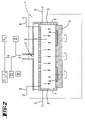
- FIG. 1 shows a highly diagrammatic illustration of a process chamber in a reactor of a first exemplary embodiment
- FIG. 2 shows a second exemplary embodiment of a process chamber in a reactor
- FIG. 3 to FIG. 8 show various layer structures produced using the method according to the invention.
- the apparatus illustrated in FIG. 1 is the process chamber 2 of a reactor 1 , which is only diagrammatically indicated.
- the process chamber 2 has a substrate holder 5 which extends in the horizontal plane and may consist, for example, of graphite or of coated graphite.
- This substrate holder 5 is rotationally driven in a known way. It rotates about its own axis.
- the substrate holder 5 is in the shape of a circular disk.
- Cylindrical substrate carrier plates 6 on which a substrate can be placed, are located in cylindrical pockets on the substrate holder. These substrate carrier plates 6 are driven in rotation by means of a gas cushion. In the process, they rotate about their own axis.
- a gas outlet member 7 opens out in the center of the process chamber 2 .
- this gas outlet member 7 has two gas outlet openings, namely a peripheral outlet opening, through which, by way of example, trimethylgallium can enter the process chamber in gas form, and a central outlet opening, through which arsine can be introduced into the process chamber.
- the gas inlet member 7 projects through an opening in a process chamber cover 4 which extends parallel to the substrate holders.
- the periphery of the process chamber 2 is surrounded by an annular wall 3 which has gas outlet openings through which the process gas can emerge from the process chamber 2 .
- the substrate holder 5 is heated from below, for example by means of infrared radiation or by means of radio waves.
- the process chamber wall 3 and the process chamber cover 4 may also be heated. The heating of the process chamber wall and the process chamber cover serves to minimize the parasitic growth.
- the process chamber cover 4 and the process chamber wall 3 may be configured to be electrically conductive. However, they may also have electrically conductive zones. These electrically conductive zones are connected to electrodes 8 , 9 .
- a radiofrequency electromagnetic alternating field can be connected to these electrodes, so that given a suitable vapor phase composition inside the process chamber 2 a plasma can form therein.
- This plasma generates hydrogen, chlorine or fluorine radicals, by means of which a silicon coating on the process chamber cover 4 or the process chamber wall 3 can be etched away.
- HCl to be introduced through the gas inlet member 7 , by means of which a coverage of gallium arsenide on the process chamber wall and the process chamber cover 2 can be etched away.
- the introduction of HCl and/or the generation of the radicals also serves to etch the surface of the substrate holder 5 . It is possible to partially etch both the surfaces of the substrate and of the layers deposited on the substrates.
- the exemplary embodiment illustrated in FIG. 2 differs from the exemplary embodiment illustrated in FIG. 1 substantially with regard to the shape of the gas inlet member 7 .
- the gas inlet member 7 is a multi-passage gas inlet system, in which the passages are separated from one another up to their openings
- the gas inlet member 7 illustrated in FIG. 2 is a type of “showerhead”. This gas inlet system has a central chamber, from which a large number of openings disposed in grid form open out into the process chamber 2 .
- reference numeral 10 denotes various gas mass flow regulators.
- the apparatus in each case has gas mass flow regulators for trimethylindium, trimethylgallium, phosphine, arsine, silane, germane, HCl, chlorine and fluorine, and also hydrogen.
- the gas mass flow regulators 10 may be of any desired structure. It is advantageous if a gas mass flow regulator 10 of at least one of the crystal-forming gases, for example trimethylindium, trimethylgallium, phosphine, arsine, silane or germane, is dimensioned in such a way that this starting substance can be used both as a crystal-forming starting substance and as a dopant.
- the gas mass flow regulator 10 passes a gas mass which is reduced by several powers of 10 into the gas inlet member 7 . Reducing the gas mass flow of the corresponding starting substance to such an extent can be effected, for example, by suitable dilution. What is important, however, is that the starting substance in question can be used both to form crystals and in just trace form to dope a different crystal.
- the method according to the invention is explained on the basis of the vertical layer structures illustrated in FIGS. 3 to 8 .
- the substrate material indicated is silicon, for the sake of simplicity.
- silicon/germanium is deposited on the silicon substrate in single crystal form.
- a silicon layer is deposited on this silicon/germanium layer. This is followed by deposition of gallium arsenide.
- the substrate holder 5 is heated to a temperature of approximately 1000° C. Then, silane and germane are introduced into the process chamber through the gas inlet member 7 . A silicon/germanium layer is formed on the silicon substrate. Then, to deposit the silicon layer, silane alone is introduced into the process chamber 2 through the gas inlet member, so that the silicon layer is deposited. Parasitic growth leads to a small amount of material also being deposited on the wall 3 of the process chamber and/or the process chamber cover 4 . The coverage is minimized there by the process chamber wall 3 and the reactor cover 4 also being heated.
- the parasitic deposits on the reactor wall 3 and the reactor cover 4 are etched away. This is effected by means of a hydrogen, chlorine or fluorine plasma.
- a hydrogen, chlorine or fluorine plasma For this purpose, chlorine or HCl or fluorine or hydrogen is introduced into the process chamber.
- a plasma is ignited in the process chamber by means of the electrodes 8 and 9 .
- the free radicals which are then formed etch away the deposits in the region of the plasma.
- gallium arsenide is deposited.
- the deposition of gallium arsenide may be preceded by an etching step or a passivation step.
- an oxide layer is deposited on the silicon substrate.
- a gallium arsenide layer is deposited on this oxide layer.
- gallium arsenide is deposited on a silicon/germanium layer deposited on the substrate. This gallium arsenide layer is then covered with a silicon layer. A further etching or passivation step may be carried out before the silicon covering layer is deposited.
- HCl can be introduced into the reactor in order to remove the gallium arsenide which has been parasitically deposited on the process chamber wall 3 , the substrate holder 5 or the reactor cover 4 . This HCl etches away the parasitically grown gallium arsenide. This etching step may even partially etch the gallium arsenide layer itself.
- the deposition of the silicon covering layer is preceded by the deposition of a passivation layer, so that it is impossible for any gallium or arsenide to be vaporized out of the gallium arsenide deposits.
- first of all silicon/germanium is deposited on the silicon substrate. This layer is followed by a gallium arsenide coating.
- the covering layer provided in this case is silicon/germanium.
- the method according to the invention is effected by loading a reactor with one or more substrates.
- the substrates are, for example, laid onto the substrate carrier plates 6 . However, it is also possible to lay just one substrate onto a non-rotatable substrate holder.
- the process chamber is heated to the deposition temperature for silicon. This deposition temperature may be approximately 1000° C.
- silane is introduced into the process chamber 2 through the gas inlet member 7 .
- the gas mass flow of the silane is set by means of the gas mass flow regulator 10 .
- the gas mass flow is set to be sufficient to effect correspondingly extensive layer growth.
- the silane flow is set to zero.
- silane is used as starting substance to build up the layer.
- arsine or trimethylgallium or alternatively phosphine or trimethylindium it is also possible for arsine or trimethylgallium or alternatively phosphine or trimethylindium to be introduced into the process chamber 2 through the gas inlet member 7 .
- the mass flow of this second starting substance is, however, considerably lower, for example by a factor of 1000, than the mass flow of silane, and consequently this second starting substance does not build up the crystal, but rather is only responsible for doping the crystal.
- this first semiconductor layer has been deposited from silane or a silane/germane mixture as first process gas
- a second semiconductor layer is effected by introducing a second starting substance and in particular a mixture of two second starting substances into the process chamber as process gas.
- the second process gas is then formed by a mixture of arsine or trimethylgallium or phosphine and trimethylindium or a mixture of all four second starting substances.
- This second process gas is then introduced into the process chamber 2 through the gas inlet member 7 at a reduced deposition temperature. In this way, a III-V layer is deposited on the substrates or on the previously deposited layers of silicon or silicon/germanium.
- This layer has a different crystal than the IV crystal layer consisting of silicon or silicon/germanium.
- silane it is also possible for silane to be introduced into the process chamber in addition to the abovementioned crystal-forming starting substances.
- the gas mass flow of the silane is considerably lower than the gas mass flow of, for example, arsine and trimethylindium.
- the layer substantially comprises gallium arsenide and only includes traces of silicon. In this case, silicon is only a dopant.
- an intermediate etching step after the deposition of the first layer.
- the process chamber wall 3 , the process chamber cover 4 and regions of the substrate holder 5 are etched. Any substances which may have been deposited during deposition of the silicon layer or there are removed during the etching step.
- This etching step may even partially etch the surface of the silicon layer.
- a plasma is preferably used to etch away parasitic silicon.
- fluorine, chlorine or HCl is introduced into the vapor phase.
- radicals are formed from these gases and remove deposits from the process chamber wall 3 and the process chamber cover 4 .
- this interlayer is deposited in such a way that primarily the process chamber wall 3 and the process chamber cover 4 are covered. Then, the temperature of the process chamber wall 3 and/or the process chamber cover 4 is controlled in a suitable way.
- the process parameters are selected in such a way that as little material as possible is deposited on the process chamber wall and the process chamber cover during the step of coating the substrate. In the intermediate coating step, however, the process parameters are set in such a way that substantially only the deposits are coated.
- Pure HCl without plasma can be used to remove parasitic growth of gallium arsenide or indium phosphide.
- the etching step will not only remove the deposits from the process chamber wall and the process chamber cover but also will partially etch the layer surface on the substrate. This is particularly advantageous if the coating is to take place with the formation of monolayer solid solutions between the individual layers.
- the formation of a monolayer solid solution in the transition region is of particular benefit to the bonding of the layers on one another and/or to defect-free growth.
- III-V compound semiconductors it is also possible to deposit II-VI compound semiconductors.
Abstract
Description
-
- (a.) one or more elements from main group V,
- (b.) elements from main groups III and V, or
- (c.) elements from main groups II and VI,
Claims (11)
Applications Claiming Priority (3)
| Application Number | Priority Date | Filing Date | Title |
|---|---|---|---|
| DE10163394.7 | 2001-12-21 | ||
| DE10163394A DE10163394A1 (en) | 2001-12-21 | 2001-12-21 | Method and device for depositing crystalline layers and on crystalline substrates |
| PCT/EP2002/013830 WO2003054256A2 (en) | 2001-12-21 | 2002-12-06 | Method and device for depositing crystalline layers on crystalline substrates |
Related Parent Applications (1)
| Application Number | Title | Priority Date | Filing Date |
|---|---|---|---|
| PCT/EP2002/013830 Continuation WO2003054256A2 (en) | 2001-12-21 | 2002-12-06 | Method and device for depositing crystalline layers on crystalline substrates |
Publications (2)
| Publication Number | Publication Date |
|---|---|
| US20050026402A1 US20050026402A1 (en) | 2005-02-03 |
| US7033921B2 true US7033921B2 (en) | 2006-04-25 |
Family
ID=7710456
Family Applications (1)
| Application Number | Title | Priority Date | Filing Date |
|---|---|---|---|
| US10/872,920 Expired - Fee Related US7033921B2 (en) | 2001-12-21 | 2004-06-21 | Method and device for depositing crystalline layers on crystalline substrates |
Country Status (6)
| Country | Link |
|---|---|
| US (1) | US7033921B2 (en) |
| JP (1) | JP2005513793A (en) |
| KR (1) | KR20040068596A (en) |
| AU (1) | AU2002366860A1 (en) |
| DE (1) | DE10163394A1 (en) |
| WO (1) | WO2003054256A2 (en) |
Cited By (17)
| Publication number | Priority date | Publication date | Assignee | Title |
|---|---|---|---|---|
| US20040005731A1 (en) * | 2000-09-01 | 2004-01-08 | Holger Jurgensen | Device and method for the depostion of, in particular, crystalline layers on, in particular, crystalline substrates |
| US20090149008A1 (en) * | 2007-10-05 | 2009-06-11 | Applied Materials, Inc. | Method for depositing group iii/v compounds |
| US20100215854A1 (en) * | 2007-06-24 | 2010-08-26 | Burrows Brian H | Hvpe showerhead design |
| US20100258052A1 (en) * | 2009-04-10 | 2010-10-14 | Applied Materials, Inc. | Hvpe precursor source hardware |
| US20100261340A1 (en) * | 2009-04-10 | 2010-10-14 | Applied Materials, Inc. | Cluster tool for leds |
| US20100273290A1 (en) * | 2009-04-28 | 2010-10-28 | Applied Materials, Inc. | Mocvd single chamber split process for led manufacturing |
| US20100273318A1 (en) * | 2009-04-24 | 2010-10-28 | Applied Materials, Inc. | Substrate pretreatment for subsequent high temperature group iii depositions |
| US20100279020A1 (en) * | 2009-04-29 | 2010-11-04 | Applied Materials, Inc. | METHOD OF FORMING IN-SITU PRE-GaN DEPOSITION LAYER IN HVPE |
| US8361892B2 (en) | 2010-04-14 | 2013-01-29 | Applied Materials, Inc. | Multiple precursor showerhead with by-pass ports |
| US9057128B2 (en) | 2011-03-18 | 2015-06-16 | Applied Materials, Inc. | Multiple level showerhead design |
| US9427762B2 (en) | 2013-02-23 | 2016-08-30 | Hermes-Epitek Corporation | Gas injector and cover plate assembly for semiconductor equipment |
| US9799736B1 (en) | 2016-07-20 | 2017-10-24 | International Business Machines Corporation | High acceptor level doping in silicon germanium |
| US10403515B2 (en) * | 2015-09-24 | 2019-09-03 | Applied Materials, Inc. | Loadlock integrated bevel etcher system |
| DE102019008930A1 (en) * | 2019-12-20 | 2021-06-24 | Azur Space Solar Power Gmbh | Gas phase epitaxy method |
| DE102019008931A1 (en) * | 2019-12-20 | 2021-06-24 | Azur Space Solar Power Gmbh | Gas phase epitaxy method |
| DE102019008929A1 (en) * | 2019-12-20 | 2021-06-24 | Azur Space Solar Power Gmbh | Gas phase epitaxy method |
| US11955334B2 (en) | 2019-12-20 | 2024-04-09 | Azur Space Solar Power Gmbh | Vapor phase epitaxy method |
Families Citing this family (262)
| Publication number | Priority date | Publication date | Assignee | Title |
|---|---|---|---|---|
| KR100674872B1 (en) * | 2005-06-03 | 2007-01-30 | 삼성전기주식회사 | Chemical Vapor Deposition Apparatus for Multiple Substrates |
| KR100703087B1 (en) * | 2005-08-08 | 2007-04-06 | 삼성전기주식회사 | Chemical Vapor Deposition Apparatus for Multiple Substrates |
| KR101316947B1 (en) * | 2005-11-01 | 2013-10-15 | 메사추세츠 인스티튜트 오브 테크놀로지 | Monolithically integrated semiconductor materials and devices |
| KR100838195B1 (en) * | 2006-03-06 | 2008-06-13 | 서울옵토디바이스주식회사 | Method for fabricating a light emitting diode of a nitride compound semiconductor and a light emitting diode fabricated by the method |
| DE102006022534A1 (en) * | 2006-05-15 | 2007-11-22 | Aixtron Ag | Source container one VPE reactor |
| KR100729264B1 (en) * | 2006-05-30 | 2007-06-15 | 삼성전자주식회사 | Gas injector and apparatus for manufacturing a wafer having the sasme |
| DE102007024798A1 (en) | 2007-05-25 | 2008-11-27 | Aixtron Ag | Device for depositing nitrogen and gallium, indium or aluminum containing semiconductor layers on substrate, comprises process chamber, first inlet for gallium chloride-containing process gas, and second inlet for ammonia-containing gas |
| US9394608B2 (en) | 2009-04-06 | 2016-07-19 | Asm America, Inc. | Semiconductor processing reactor and components thereof |
| US8802201B2 (en) | 2009-08-14 | 2014-08-12 | Asm America, Inc. | Systems and methods for thin-film deposition of metal oxides using excited nitrogen-oxygen species |
| US20110237051A1 (en) * | 2010-03-26 | 2011-09-29 | Kenneth Lee Hess | Process and apparatus for deposition of multicomponent semiconductor layers |
| KR100996210B1 (en) * | 2010-04-12 | 2010-11-24 | 세메스 주식회사 | Gas injection unit and apparatus and method for depositing thin layer with the same |
| DE102011002145B4 (en) * | 2011-04-18 | 2023-02-09 | Aixtron Se | Device and method for large-area deposition of semiconductor layers with gas-separated HCl feed |
| DE102011002146B4 (en) * | 2011-04-18 | 2023-03-09 | Aixtron Se | Apparatus and method for depositing semiconductor layers with HCI addition to suppress parasitic growth |
| US9312155B2 (en) | 2011-06-06 | 2016-04-12 | Asm Japan K.K. | High-throughput semiconductor-processing apparatus equipped with multiple dual-chamber modules |
| US10854498B2 (en) | 2011-07-15 | 2020-12-01 | Asm Ip Holding B.V. | Wafer-supporting device and method for producing same |
| US20130023129A1 (en) | 2011-07-20 | 2013-01-24 | Asm America, Inc. | Pressure transmitter for a semiconductor processing environment |
| US9017481B1 (en) | 2011-10-28 | 2015-04-28 | Asm America, Inc. | Process feed management for semiconductor substrate processing |
| DE102011056538A1 (en) * | 2011-12-16 | 2013-06-20 | Aixtron Se | Method for removing unwanted residues of process chamber of chemical vapor deposition reactor, involves forming non-volatile intermediate, so that surface coverage degree of residue is increased/decreased at respective phases of cycle |
| US20130171350A1 (en) * | 2011-12-29 | 2013-07-04 | Intermolecular Inc. | High Throughput Processing Using Metal Organic Chemical Vapor Deposition |
| DE102012102661B4 (en) * | 2012-03-28 | 2024-01-18 | Aixtron Se | Method for cleaning the walls of a process chamber of a CVD reactor |
| US10714315B2 (en) | 2012-10-12 | 2020-07-14 | Asm Ip Holdings B.V. | Semiconductor reaction chamber showerhead |
| US10683571B2 (en) | 2014-02-25 | 2020-06-16 | Asm Ip Holding B.V. | Gas supply manifold and method of supplying gases to chamber using same |
| US10167557B2 (en) | 2014-03-18 | 2019-01-01 | Asm Ip Holding B.V. | Gas distribution system, reactor including the system, and methods of using the same |
| US11015245B2 (en) | 2014-03-19 | 2021-05-25 | Asm Ip Holding B.V. | Gas-phase reactor and system having exhaust plenum and components thereof |
| US10858737B2 (en) | 2014-07-28 | 2020-12-08 | Asm Ip Holding B.V. | Showerhead assembly and components thereof |
| US9890456B2 (en) | 2014-08-21 | 2018-02-13 | Asm Ip Holding B.V. | Method and system for in situ formation of gas-phase compounds |
| US10941490B2 (en) | 2014-10-07 | 2021-03-09 | Asm Ip Holding B.V. | Multiple temperature range susceptor, assembly, reactor and system including the susceptor, and methods of using the same |
| US10276355B2 (en) | 2015-03-12 | 2019-04-30 | Asm Ip Holding B.V. | Multi-zone reactor, system including the reactor, and method of using the same |
| US10458018B2 (en) | 2015-06-26 | 2019-10-29 | Asm Ip Holding B.V. | Structures including metal carbide material, devices including the structures, and methods of forming same |
| US10600673B2 (en) | 2015-07-07 | 2020-03-24 | Asm Ip Holding B.V. | Magnetic susceptor to baseplate seal |
| US10211308B2 (en) | 2015-10-21 | 2019-02-19 | Asm Ip Holding B.V. | NbMC layers |
| US11139308B2 (en) | 2015-12-29 | 2021-10-05 | Asm Ip Holding B.V. | Atomic layer deposition of III-V compounds to form V-NAND devices |
| US10529554B2 (en) | 2016-02-19 | 2020-01-07 | Asm Ip Holding B.V. | Method for forming silicon nitride film selectively on sidewalls or flat surfaces of trenches |
| US10190213B2 (en) | 2016-04-21 | 2019-01-29 | Asm Ip Holding B.V. | Deposition of metal borides |
| US10865475B2 (en) | 2016-04-21 | 2020-12-15 | Asm Ip Holding B.V. | Deposition of metal borides and silicides |
| US10032628B2 (en) | 2016-05-02 | 2018-07-24 | Asm Ip Holding B.V. | Source/drain performance through conformal solid state doping |
| US10367080B2 (en) | 2016-05-02 | 2019-07-30 | Asm Ip Holding B.V. | Method of forming a germanium oxynitride film |
| US11453943B2 (en) | 2016-05-25 | 2022-09-27 | Asm Ip Holding B.V. | Method for forming carbon-containing silicon/metal oxide or nitride film by ALD using silicon precursor and hydrocarbon precursor |
| US10612137B2 (en) | 2016-07-08 | 2020-04-07 | Asm Ip Holdings B.V. | Organic reactants for atomic layer deposition |
| US9859151B1 (en) | 2016-07-08 | 2018-01-02 | Asm Ip Holding B.V. | Selective film deposition method to form air gaps |
| US10714385B2 (en) | 2016-07-19 | 2020-07-14 | Asm Ip Holding B.V. | Selective deposition of tungsten |
| US9887082B1 (en) | 2016-07-28 | 2018-02-06 | Asm Ip Holding B.V. | Method and apparatus for filling a gap |
| US9812320B1 (en) | 2016-07-28 | 2017-11-07 | Asm Ip Holding B.V. | Method and apparatus for filling a gap |
| KR102532607B1 (en) | 2016-07-28 | 2023-05-15 | 에이에스엠 아이피 홀딩 비.브이. | Substrate processing apparatus and method of operating the same |
| US10643826B2 (en) | 2016-10-26 | 2020-05-05 | Asm Ip Holdings B.V. | Methods for thermally calibrating reaction chambers |
| US11532757B2 (en) | 2016-10-27 | 2022-12-20 | Asm Ip Holding B.V. | Deposition of charge trapping layers |
| US10229833B2 (en) | 2016-11-01 | 2019-03-12 | Asm Ip Holding B.V. | Methods for forming a transition metal nitride film on a substrate by atomic layer deposition and related semiconductor device structures |
| US10714350B2 (en) | 2016-11-01 | 2020-07-14 | ASM IP Holdings, B.V. | Methods for forming a transition metal niobium nitride film on a substrate by atomic layer deposition and related semiconductor device structures |
| US10643904B2 (en) | 2016-11-01 | 2020-05-05 | Asm Ip Holdings B.V. | Methods for forming a semiconductor device and related semiconductor device structures |
| KR102546317B1 (en) | 2016-11-15 | 2023-06-21 | 에이에스엠 아이피 홀딩 비.브이. | Gas supply unit and substrate processing apparatus including the same |
| KR20180068582A (en) | 2016-12-14 | 2018-06-22 | 에이에스엠 아이피 홀딩 비.브이. | Substrate processing apparatus |
| US11581186B2 (en) | 2016-12-15 | 2023-02-14 | Asm Ip Holding B.V. | Sequential infiltration synthesis apparatus |
| US11447861B2 (en) | 2016-12-15 | 2022-09-20 | Asm Ip Holding B.V. | Sequential infiltration synthesis apparatus and a method of forming a patterned structure |
| KR20180070971A (en) | 2016-12-19 | 2018-06-27 | 에이에스엠 아이피 홀딩 비.브이. | Substrate processing apparatus |
| US10269558B2 (en) | 2016-12-22 | 2019-04-23 | Asm Ip Holding B.V. | Method of forming a structure on a substrate |
| US10867788B2 (en) | 2016-12-28 | 2020-12-15 | Asm Ip Holding B.V. | Method of forming a structure on a substrate |
| US11390950B2 (en) | 2017-01-10 | 2022-07-19 | Asm Ip Holding B.V. | Reactor system and method to reduce residue buildup during a film deposition process |
| US10655221B2 (en) | 2017-02-09 | 2020-05-19 | Asm Ip Holding B.V. | Method for depositing oxide film by thermal ALD and PEALD |
| US10468261B2 (en) | 2017-02-15 | 2019-11-05 | Asm Ip Holding B.V. | Methods for forming a metallic film on a substrate by cyclical deposition and related semiconductor device structures |
| CN106948001B (en) * | 2017-03-17 | 2019-06-21 | 电子科技大学 | A kind of bottle-neck reaction tube and high-throughput two-dimentional single crystal furnace device |
| US10529563B2 (en) | 2017-03-29 | 2020-01-07 | Asm Ip Holdings B.V. | Method for forming doped metal oxide films on a substrate by cyclical deposition and related semiconductor device structures |
| KR102369676B1 (en) | 2017-04-10 | 2022-03-04 | 삼성디스플레이 주식회사 | Apparatus and method for manufacturing a display apparatus |
| KR102457289B1 (en) | 2017-04-25 | 2022-10-21 | 에이에스엠 아이피 홀딩 비.브이. | Method for depositing a thin film and manufacturing a semiconductor device |
| US10770286B2 (en) | 2017-05-08 | 2020-09-08 | Asm Ip Holdings B.V. | Methods for selectively forming a silicon nitride film on a substrate and related semiconductor device structures |
| US10892156B2 (en) | 2017-05-08 | 2021-01-12 | Asm Ip Holding B.V. | Methods for forming a silicon nitride film on a substrate and related semiconductor device structures |
| US11306395B2 (en) | 2017-06-28 | 2022-04-19 | Asm Ip Holding B.V. | Methods for depositing a transition metal nitride film on a substrate by atomic layer deposition and related deposition apparatus |
| US10685834B2 (en) | 2017-07-05 | 2020-06-16 | Asm Ip Holdings B.V. | Methods for forming a silicon germanium tin layer and related semiconductor device structures |
| KR20190009245A (en) | 2017-07-18 | 2019-01-28 | 에이에스엠 아이피 홀딩 비.브이. | Methods for forming a semiconductor device structure and related semiconductor device structures |
| US10541333B2 (en) | 2017-07-19 | 2020-01-21 | Asm Ip Holding B.V. | Method for depositing a group IV semiconductor and related semiconductor device structures |
| US11374112B2 (en) * | 2017-07-19 | 2022-06-28 | Asm Ip Holding B.V. | Method for depositing a group IV semiconductor and related semiconductor device structures |
| US11018002B2 (en) | 2017-07-19 | 2021-05-25 | Asm Ip Holding B.V. | Method for selectively depositing a Group IV semiconductor and related semiconductor device structures |
| US10590535B2 (en) | 2017-07-26 | 2020-03-17 | Asm Ip Holdings B.V. | Chemical treatment, deposition and/or infiltration apparatus and method for using the same |
| US10770336B2 (en) | 2017-08-08 | 2020-09-08 | Asm Ip Holding B.V. | Substrate lift mechanism and reactor including same |
| US10692741B2 (en) | 2017-08-08 | 2020-06-23 | Asm Ip Holdings B.V. | Radiation shield |
| US11769682B2 (en) | 2017-08-09 | 2023-09-26 | Asm Ip Holding B.V. | Storage apparatus for storing cassettes for substrates and processing apparatus equipped therewith |
| US11139191B2 (en) | 2017-08-09 | 2021-10-05 | Asm Ip Holding B.V. | Storage apparatus for storing cassettes for substrates and processing apparatus equipped therewith |
| US10249524B2 (en) | 2017-08-09 | 2019-04-02 | Asm Ip Holding B.V. | Cassette holder assembly for a substrate cassette and holding member for use in such assembly |
| USD900036S1 (en) | 2017-08-24 | 2020-10-27 | Asm Ip Holding B.V. | Heater electrical connector and adapter |
| US11830730B2 (en) | 2017-08-29 | 2023-11-28 | Asm Ip Holding B.V. | Layer forming method and apparatus |
| US11056344B2 (en) | 2017-08-30 | 2021-07-06 | Asm Ip Holding B.V. | Layer forming method |
| US11295980B2 (en) | 2017-08-30 | 2022-04-05 | Asm Ip Holding B.V. | Methods for depositing a molybdenum metal film over a dielectric surface of a substrate by a cyclical deposition process and related semiconductor device structures |
| KR102491945B1 (en) | 2017-08-30 | 2023-01-26 | 에이에스엠 아이피 홀딩 비.브이. | Substrate processing apparatus |
| KR102630301B1 (en) | 2017-09-21 | 2024-01-29 | 에이에스엠 아이피 홀딩 비.브이. | Method of sequential infiltration synthesis treatment of infiltrateable material and structures and devices formed using same |
| US10844484B2 (en) | 2017-09-22 | 2020-11-24 | Asm Ip Holding B.V. | Apparatus for dispensing a vapor phase reactant to a reaction chamber and related methods |
| US10658205B2 (en) | 2017-09-28 | 2020-05-19 | Asm Ip Holdings B.V. | Chemical dispensing apparatus and methods for dispensing a chemical to a reaction chamber |
| US10403504B2 (en) | 2017-10-05 | 2019-09-03 | Asm Ip Holding B.V. | Method for selectively depositing a metallic film on a substrate |
| US10319588B2 (en) | 2017-10-10 | 2019-06-11 | Asm Ip Holding B.V. | Method for depositing a metal chalcogenide on a substrate by cyclical deposition |
| US10923344B2 (en) | 2017-10-30 | 2021-02-16 | Asm Ip Holding B.V. | Methods for forming a semiconductor structure and related semiconductor structures |
| KR102443047B1 (en) | 2017-11-16 | 2022-09-14 | 에이에스엠 아이피 홀딩 비.브이. | Method of processing a substrate and a device manufactured by the same |
| US10910262B2 (en) | 2017-11-16 | 2021-02-02 | Asm Ip Holding B.V. | Method of selectively depositing a capping layer structure on a semiconductor device structure |
| US11022879B2 (en) | 2017-11-24 | 2021-06-01 | Asm Ip Holding B.V. | Method of forming an enhanced unexposed photoresist layer |
| JP7214724B2 (en) | 2017-11-27 | 2023-01-30 | エーエスエム アイピー ホールディング ビー.ブイ. | Storage device for storing wafer cassettes used in batch furnaces |
| TWI791689B (en) | 2017-11-27 | 2023-02-11 | 荷蘭商Asm智慧財產控股私人有限公司 | Apparatus including a clean mini environment |
| US10872771B2 (en) | 2018-01-16 | 2020-12-22 | Asm Ip Holding B. V. | Method for depositing a material film on a substrate within a reaction chamber by a cyclical deposition process and related device structures |
| WO2019142055A2 (en) | 2018-01-19 | 2019-07-25 | Asm Ip Holding B.V. | Method for depositing a gap-fill layer by plasma-assisted deposition |
| TWI799494B (en) | 2018-01-19 | 2023-04-21 | 荷蘭商Asm 智慧財產控股公司 | Deposition method |
| USD903477S1 (en) | 2018-01-24 | 2020-12-01 | Asm Ip Holdings B.V. | Metal clamp |
| US11018047B2 (en) | 2018-01-25 | 2021-05-25 | Asm Ip Holding B.V. | Hybrid lift pin |
| USD880437S1 (en) | 2018-02-01 | 2020-04-07 | Asm Ip Holding B.V. | Gas supply plate for semiconductor manufacturing apparatus |
| US11081345B2 (en) | 2018-02-06 | 2021-08-03 | Asm Ip Holding B.V. | Method of post-deposition treatment for silicon oxide film |
| US11685991B2 (en) | 2018-02-14 | 2023-06-27 | Asm Ip Holding B.V. | Method for depositing a ruthenium-containing film on a substrate by a cyclical deposition process |
| US10896820B2 (en) | 2018-02-14 | 2021-01-19 | Asm Ip Holding B.V. | Method for depositing a ruthenium-containing film on a substrate by a cyclical deposition process |
| US10731249B2 (en) | 2018-02-15 | 2020-08-04 | Asm Ip Holding B.V. | Method of forming a transition metal containing film on a substrate by a cyclical deposition process, a method for supplying a transition metal halide compound to a reaction chamber, and related vapor deposition apparatus |
| US10658181B2 (en) | 2018-02-20 | 2020-05-19 | Asm Ip Holding B.V. | Method of spacer-defined direct patterning in semiconductor fabrication |
| KR102636427B1 (en) | 2018-02-20 | 2024-02-13 | 에이에스엠 아이피 홀딩 비.브이. | Substrate processing method and apparatus |
| US10975470B2 (en) | 2018-02-23 | 2021-04-13 | Asm Ip Holding B.V. | Apparatus for detecting or monitoring for a chemical precursor in a high temperature environment |
| US11473195B2 (en) | 2018-03-01 | 2022-10-18 | Asm Ip Holding B.V. | Semiconductor processing apparatus and a method for processing a substrate |
| US11629406B2 (en) | 2018-03-09 | 2023-04-18 | Asm Ip Holding B.V. | Semiconductor processing apparatus comprising one or more pyrometers for measuring a temperature of a substrate during transfer of the substrate |
| US11114283B2 (en) | 2018-03-16 | 2021-09-07 | Asm Ip Holding B.V. | Reactor, system including the reactor, and methods of manufacturing and using same |
| KR102646467B1 (en) | 2018-03-27 | 2024-03-11 | 에이에스엠 아이피 홀딩 비.브이. | Method of forming an electrode on a substrate and a semiconductor device structure including an electrode |
| US11088002B2 (en) | 2018-03-29 | 2021-08-10 | Asm Ip Holding B.V. | Substrate rack and a substrate processing system and method |
| US11230766B2 (en) | 2018-03-29 | 2022-01-25 | Asm Ip Holding B.V. | Substrate processing apparatus and method |
| KR102501472B1 (en) | 2018-03-30 | 2023-02-20 | 에이에스엠 아이피 홀딩 비.브이. | Substrate processing method |
| TWI811348B (en) | 2018-05-08 | 2023-08-11 | 荷蘭商Asm 智慧財產控股公司 | Methods for depositing an oxide film on a substrate by a cyclical deposition process and related device structures |
| KR20190129718A (en) | 2018-05-11 | 2019-11-20 | 에이에스엠 아이피 홀딩 비.브이. | Methods for forming a doped metal carbide film on a substrate and related semiconductor device structures |
| KR102596988B1 (en) | 2018-05-28 | 2023-10-31 | 에이에스엠 아이피 홀딩 비.브이. | Method of processing a substrate and a device manufactured by the same |
| US11718913B2 (en) | 2018-06-04 | 2023-08-08 | Asm Ip Holding B.V. | Gas distribution system and reactor system including same |
| TW202013553A (en) | 2018-06-04 | 2020-04-01 | 荷蘭商Asm 智慧財產控股公司 | Wafer handling chamber with moisture reduction |
| US11286562B2 (en) | 2018-06-08 | 2022-03-29 | Asm Ip Holding B.V. | Gas-phase chemical reactor and method of using same |
| US10797133B2 (en) | 2018-06-21 | 2020-10-06 | Asm Ip Holding B.V. | Method for depositing a phosphorus doped silicon arsenide film and related semiconductor device structures |
| KR102568797B1 (en) | 2018-06-21 | 2023-08-21 | 에이에스엠 아이피 홀딩 비.브이. | Substrate processing system |
| CN112292478A (en) | 2018-06-27 | 2021-01-29 | Asm Ip私人控股有限公司 | Cyclic deposition methods for forming metal-containing materials and films and structures containing metal-containing materials |
| JP2021529880A (en) | 2018-06-27 | 2021-11-04 | エーエスエム・アイピー・ホールディング・ベー・フェー | Periodic deposition methods for forming metal-containing materials and films and structures containing metal-containing materials |
| US10612136B2 (en) | 2018-06-29 | 2020-04-07 | ASM IP Holding, B.V. | Temperature-controlled flange and reactor system including same |
| KR20200002519A (en) | 2018-06-29 | 2020-01-08 | 에이에스엠 아이피 홀딩 비.브이. | Method for depositing a thin film and manufacturing a semiconductor device |
| US10755922B2 (en) | 2018-07-03 | 2020-08-25 | Asm Ip Holding B.V. | Method for depositing silicon-free carbon-containing film as gap-fill layer by pulse plasma-assisted deposition |
| US10388513B1 (en) | 2018-07-03 | 2019-08-20 | Asm Ip Holding B.V. | Method for depositing silicon-free carbon-containing film as gap-fill layer by pulse plasma-assisted deposition |
| US10767789B2 (en) | 2018-07-16 | 2020-09-08 | Asm Ip Holding B.V. | Diaphragm valves, valve components, and methods for forming valve components |
| US11053591B2 (en) | 2018-08-06 | 2021-07-06 | Asm Ip Holding B.V. | Multi-port gas injection system and reactor system including same |
| US10883175B2 (en) | 2018-08-09 | 2021-01-05 | Asm Ip Holding B.V. | Vertical furnace for processing substrates and a liner for use therein |
| US10829852B2 (en) | 2018-08-16 | 2020-11-10 | Asm Ip Holding B.V. | Gas distribution device for a wafer processing apparatus |
| US11430674B2 (en) | 2018-08-22 | 2022-08-30 | Asm Ip Holding B.V. | Sensor array, apparatus for dispensing a vapor phase reactant to a reaction chamber and related methods |
| KR20200030162A (en) | 2018-09-11 | 2020-03-20 | 에이에스엠 아이피 홀딩 비.브이. | Method for deposition of a thin film |
| US11024523B2 (en) | 2018-09-11 | 2021-06-01 | Asm Ip Holding B.V. | Substrate processing apparatus and method |
| US11049751B2 (en) | 2018-09-14 | 2021-06-29 | Asm Ip Holding B.V. | Cassette supply system to store and handle cassettes and processing apparatus equipped therewith |
| CN110970344A (en) | 2018-10-01 | 2020-04-07 | Asm Ip控股有限公司 | Substrate holding apparatus, system including the same, and method of using the same |
| US11232963B2 (en) | 2018-10-03 | 2022-01-25 | Asm Ip Holding B.V. | Substrate processing apparatus and method |
| KR102592699B1 (en) | 2018-10-08 | 2023-10-23 | 에이에스엠 아이피 홀딩 비.브이. | Substrate support unit and apparatuses for depositing thin film and processing the substrate including the same |
| US10847365B2 (en) | 2018-10-11 | 2020-11-24 | Asm Ip Holding B.V. | Method of forming conformal silicon carbide film by cyclic CVD |
| US10811256B2 (en) | 2018-10-16 | 2020-10-20 | Asm Ip Holding B.V. | Method for etching a carbon-containing feature |
| KR102605121B1 (en) | 2018-10-19 | 2023-11-23 | 에이에스엠 아이피 홀딩 비.브이. | Substrate processing apparatus and substrate processing method |
| KR102546322B1 (en) | 2018-10-19 | 2023-06-21 | 에이에스엠 아이피 홀딩 비.브이. | Substrate processing apparatus and substrate processing method |
| USD948463S1 (en) | 2018-10-24 | 2022-04-12 | Asm Ip Holding B.V. | Susceptor for semiconductor substrate supporting apparatus |
| US11087997B2 (en) | 2018-10-31 | 2021-08-10 | Asm Ip Holding B.V. | Substrate processing apparatus for processing substrates |
| KR20200051105A (en) | 2018-11-02 | 2020-05-13 | 에이에스엠 아이피 홀딩 비.브이. | Substrate support unit and substrate processing apparatus including the same |
| US11572620B2 (en) | 2018-11-06 | 2023-02-07 | Asm Ip Holding B.V. | Methods for selectively depositing an amorphous silicon film on a substrate |
| US11031242B2 (en) | 2018-11-07 | 2021-06-08 | Asm Ip Holding B.V. | Methods for depositing a boron doped silicon germanium film |
| US10818758B2 (en) | 2018-11-16 | 2020-10-27 | Asm Ip Holding B.V. | Methods for forming a metal silicate film on a substrate in a reaction chamber and related semiconductor device structures |
| US10847366B2 (en) | 2018-11-16 | 2020-11-24 | Asm Ip Holding B.V. | Methods for depositing a transition metal chalcogenide film on a substrate by a cyclical deposition process |
| US11217444B2 (en) | 2018-11-30 | 2022-01-04 | Asm Ip Holding B.V. | Method for forming an ultraviolet radiation responsive metal oxide-containing film |
| KR102636428B1 (en) | 2018-12-04 | 2024-02-13 | 에이에스엠 아이피 홀딩 비.브이. | A method for cleaning a substrate processing apparatus |
| US11158513B2 (en) | 2018-12-13 | 2021-10-26 | Asm Ip Holding B.V. | Methods for forming a rhenium-containing film on a substrate by a cyclical deposition process and related semiconductor device structures |
| TW202037745A (en) | 2018-12-14 | 2020-10-16 | 荷蘭商Asm Ip私人控股有限公司 | Method of forming device structure, structure formed by the method and system for performing the method |
| TWI819180B (en) | 2019-01-17 | 2023-10-21 | 荷蘭商Asm 智慧財產控股公司 | Methods of forming a transition metal containing film on a substrate by a cyclical deposition process |
| KR20200091543A (en) | 2019-01-22 | 2020-07-31 | 에이에스엠 아이피 홀딩 비.브이. | Semiconductor processing device |
| CN111524788B (en) | 2019-02-01 | 2023-11-24 | Asm Ip私人控股有限公司 | Method for topologically selective film formation of silicon oxide |
| KR102626263B1 (en) | 2019-02-20 | 2024-01-16 | 에이에스엠 아이피 홀딩 비.브이. | Cyclical deposition method including treatment step and apparatus for same |
| JP2020136677A (en) | 2019-02-20 | 2020-08-31 | エーエスエム・アイピー・ホールディング・ベー・フェー | Periodic accumulation method for filing concave part formed inside front surface of base material, and device |
| KR20200102357A (en) | 2019-02-20 | 2020-08-31 | 에이에스엠 아이피 홀딩 비.브이. | Apparatus and methods for plug fill deposition in 3-d nand applications |
| JP2020136678A (en) | 2019-02-20 | 2020-08-31 | エーエスエム・アイピー・ホールディング・ベー・フェー | Method for filing concave part formed inside front surface of base material, and device |
| TW202100794A (en) | 2019-02-22 | 2021-01-01 | 荷蘭商Asm Ip私人控股有限公司 | Substrate processing apparatus and method for processing substrate |
| KR20200108243A (en) | 2019-03-08 | 2020-09-17 | 에이에스엠 아이피 홀딩 비.브이. | Structure Including SiOC Layer and Method of Forming Same |
| US11742198B2 (en) | 2019-03-08 | 2023-08-29 | Asm Ip Holding B.V. | Structure including SiOCN layer and method of forming same |
| KR20200108242A (en) | 2019-03-08 | 2020-09-17 | 에이에스엠 아이피 홀딩 비.브이. | Method for Selective Deposition of Silicon Nitride Layer and Structure Including Selectively-Deposited Silicon Nitride Layer |
| JP2020167398A (en) | 2019-03-28 | 2020-10-08 | エーエスエム・アイピー・ホールディング・ベー・フェー | Door opener and substrate processing apparatus provided therewith |
| KR20200116855A (en) | 2019-04-01 | 2020-10-13 | 에이에스엠 아이피 홀딩 비.브이. | Method of manufacturing semiconductor device |
| US11447864B2 (en) | 2019-04-19 | 2022-09-20 | Asm Ip Holding B.V. | Layer forming method and apparatus |
| KR20200125453A (en) | 2019-04-24 | 2020-11-04 | 에이에스엠 아이피 홀딩 비.브이. | Gas-phase reactor system and method of using same |
| KR20200130118A (en) | 2019-05-07 | 2020-11-18 | 에이에스엠 아이피 홀딩 비.브이. | Method for Reforming Amorphous Carbon Polymer Film |
| KR20200130121A (en) | 2019-05-07 | 2020-11-18 | 에이에스엠 아이피 홀딩 비.브이. | Chemical source vessel with dip tube |
| KR20200130652A (en) | 2019-05-10 | 2020-11-19 | 에이에스엠 아이피 홀딩 비.브이. | Method of depositing material onto a surface and structure formed according to the method |
| JP2020188255A (en) | 2019-05-16 | 2020-11-19 | エーエスエム アイピー ホールディング ビー.ブイ. | Wafer boat handling device, vertical batch furnace, and method |
| USD947913S1 (en) | 2019-05-17 | 2022-04-05 | Asm Ip Holding B.V. | Susceptor shaft |
| USD975665S1 (en) | 2019-05-17 | 2023-01-17 | Asm Ip Holding B.V. | Susceptor shaft |
| USD935572S1 (en) | 2019-05-24 | 2021-11-09 | Asm Ip Holding B.V. | Gas channel plate |
| USD922229S1 (en) | 2019-06-05 | 2021-06-15 | Asm Ip Holding B.V. | Device for controlling a temperature of a gas supply unit |
| KR20200141003A (en) | 2019-06-06 | 2020-12-17 | 에이에스엠 아이피 홀딩 비.브이. | Gas-phase reactor system including a gas detector |
| KR20200143254A (en) | 2019-06-11 | 2020-12-23 | 에이에스엠 아이피 홀딩 비.브이. | Method of forming an electronic structure using an reforming gas, system for performing the method, and structure formed using the method |
| USD944946S1 (en) | 2019-06-14 | 2022-03-01 | Asm Ip Holding B.V. | Shower plate |
| USD931978S1 (en) | 2019-06-27 | 2021-09-28 | Asm Ip Holding B.V. | Showerhead vacuum transport |
| KR20210005515A (en) | 2019-07-03 | 2021-01-14 | 에이에스엠 아이피 홀딩 비.브이. | Temperature control assembly for substrate processing apparatus and method of using same |
| JP2021015791A (en) | 2019-07-09 | 2021-02-12 | エーエスエム アイピー ホールディング ビー.ブイ. | Plasma device and substrate processing method using coaxial waveguide |
| CN112216646A (en) | 2019-07-10 | 2021-01-12 | Asm Ip私人控股有限公司 | Substrate supporting assembly and substrate processing device comprising same |
| KR20210010307A (en) | 2019-07-16 | 2021-01-27 | 에이에스엠 아이피 홀딩 비.브이. | Substrate processing apparatus |
| KR20210010816A (en) | 2019-07-17 | 2021-01-28 | 에이에스엠 아이피 홀딩 비.브이. | Radical assist ignition plasma system and method |
| KR20210010820A (en) | 2019-07-17 | 2021-01-28 | 에이에스엠 아이피 홀딩 비.브이. | Methods of forming silicon germanium structures |
| US11643724B2 (en) | 2019-07-18 | 2023-05-09 | Asm Ip Holding B.V. | Method of forming structures using a neutral beam |
| TW202121506A (en) | 2019-07-19 | 2021-06-01 | 荷蘭商Asm Ip私人控股有限公司 | Method of forming topology-controlled amorphous carbon polymer film |
| TW202113936A (en) | 2019-07-29 | 2021-04-01 | 荷蘭商Asm Ip私人控股有限公司 | Methods for selective deposition utilizing n-type dopants and/or alternative dopants to achieve high dopant incorporation |
| CN112309899A (en) | 2019-07-30 | 2021-02-02 | Asm Ip私人控股有限公司 | Substrate processing apparatus |
| CN112309900A (en) | 2019-07-30 | 2021-02-02 | Asm Ip私人控股有限公司 | Substrate processing apparatus |
| US11587815B2 (en) | 2019-07-31 | 2023-02-21 | Asm Ip Holding B.V. | Vertical batch furnace assembly |
| US11587814B2 (en) | 2019-07-31 | 2023-02-21 | Asm Ip Holding B.V. | Vertical batch furnace assembly |
| US11227782B2 (en) | 2019-07-31 | 2022-01-18 | Asm Ip Holding B.V. | Vertical batch furnace assembly |
| CN112323048B (en) | 2019-08-05 | 2024-02-09 | Asm Ip私人控股有限公司 | Liquid level sensor for chemical source container |
| USD965524S1 (en) | 2019-08-19 | 2022-10-04 | Asm Ip Holding B.V. | Susceptor support |
| USD965044S1 (en) | 2019-08-19 | 2022-09-27 | Asm Ip Holding B.V. | Susceptor shaft |
| JP2021031769A (en) | 2019-08-21 | 2021-03-01 | エーエスエム アイピー ホールディング ビー.ブイ. | Production apparatus of mixed gas of film deposition raw material and film deposition apparatus |
| USD949319S1 (en) | 2019-08-22 | 2022-04-19 | Asm Ip Holding B.V. | Exhaust duct |
| USD979506S1 (en) | 2019-08-22 | 2023-02-28 | Asm Ip Holding B.V. | Insulator |
| USD930782S1 (en) | 2019-08-22 | 2021-09-14 | Asm Ip Holding B.V. | Gas distributor |
| KR20210024423A (en) | 2019-08-22 | 2021-03-05 | 에이에스엠 아이피 홀딩 비.브이. | Method for forming a structure with a hole |
| USD940837S1 (en) | 2019-08-22 | 2022-01-11 | Asm Ip Holding B.V. | Electrode |
| US11286558B2 (en) | 2019-08-23 | 2022-03-29 | Asm Ip Holding B.V. | Methods for depositing a molybdenum nitride film on a surface of a substrate by a cyclical deposition process and related semiconductor device structures including a molybdenum nitride film |
| KR20210024420A (en) | 2019-08-23 | 2021-03-05 | 에이에스엠 아이피 홀딩 비.브이. | Method for depositing silicon oxide film having improved quality by peald using bis(diethylamino)silane |
| KR20210029090A (en) | 2019-09-04 | 2021-03-15 | 에이에스엠 아이피 홀딩 비.브이. | Methods for selective deposition using a sacrificial capping layer |
| KR20210029663A (en) | 2019-09-05 | 2021-03-16 | 에이에스엠 아이피 홀딩 비.브이. | Substrate processing apparatus |
| US11562901B2 (en) | 2019-09-25 | 2023-01-24 | Asm Ip Holding B.V. | Substrate processing method |
| CN112593212B (en) | 2019-10-02 | 2023-12-22 | Asm Ip私人控股有限公司 | Method for forming topologically selective silicon oxide film by cyclic plasma enhanced deposition process |
| TW202129060A (en) | 2019-10-08 | 2021-08-01 | 荷蘭商Asm Ip控股公司 | Substrate processing device, and substrate processing method |
| KR20210043460A (en) | 2019-10-10 | 2021-04-21 | 에이에스엠 아이피 홀딩 비.브이. | Method of forming a photoresist underlayer and structure including same |
| KR20210045930A (en) | 2019-10-16 | 2021-04-27 | 에이에스엠 아이피 홀딩 비.브이. | Method of Topology-Selective Film Formation of Silicon Oxide |
| US11637014B2 (en) | 2019-10-17 | 2023-04-25 | Asm Ip Holding B.V. | Methods for selective deposition of doped semiconductor material |
| KR20210047808A (en) | 2019-10-21 | 2021-04-30 | 에이에스엠 아이피 홀딩 비.브이. | Apparatus and methods for selectively etching films |
| US11646205B2 (en) | 2019-10-29 | 2023-05-09 | Asm Ip Holding B.V. | Methods of selectively forming n-type doped material on a surface, systems for selectively forming n-type doped material, and structures formed using same |
| KR20210054983A (en) | 2019-11-05 | 2021-05-14 | 에이에스엠 아이피 홀딩 비.브이. | Structures with doped semiconductor layers and methods and systems for forming same |
| US11501968B2 (en) | 2019-11-15 | 2022-11-15 | Asm Ip Holding B.V. | Method for providing a semiconductor device with silicon filled gaps |
| KR20210062561A (en) | 2019-11-20 | 2021-05-31 | 에이에스엠 아이피 홀딩 비.브이. | Method of depositing carbon-containing material on a surface of a substrate, structure formed using the method, and system for forming the structure |
| KR20210065848A (en) | 2019-11-26 | 2021-06-04 | 에이에스엠 아이피 홀딩 비.브이. | Methods for selectivley forming a target film on a substrate comprising a first dielectric surface and a second metallic surface |
| CN112951697A (en) | 2019-11-26 | 2021-06-11 | Asm Ip私人控股有限公司 | Substrate processing apparatus |
| CN112885693A (en) | 2019-11-29 | 2021-06-01 | Asm Ip私人控股有限公司 | Substrate processing apparatus |
| CN112885692A (en) | 2019-11-29 | 2021-06-01 | Asm Ip私人控股有限公司 | Substrate processing apparatus |
| JP2021090042A (en) | 2019-12-02 | 2021-06-10 | エーエスエム アイピー ホールディング ビー.ブイ. | Substrate processing apparatus and substrate processing method |
| KR20210070898A (en) | 2019-12-04 | 2021-06-15 | 에이에스엠 아이피 홀딩 비.브이. | Substrate processing apparatus |
| JP2021097227A (en) | 2019-12-17 | 2021-06-24 | エーエスエム・アイピー・ホールディング・ベー・フェー | Method of forming vanadium nitride layer and structure including vanadium nitride layer |
| KR20210080214A (en) | 2019-12-19 | 2021-06-30 | 에이에스엠 아이피 홀딩 비.브이. | Methods for filling a gap feature on a substrate and related semiconductor structures |
| KR20210095050A (en) | 2020-01-20 | 2021-07-30 | 에이에스엠 아이피 홀딩 비.브이. | Method of forming thin film and method of modifying surface of thin film |
| TW202130846A (en) | 2020-02-03 | 2021-08-16 | 荷蘭商Asm Ip私人控股有限公司 | Method of forming structures including a vanadium or indium layer |
| KR20210100010A (en) | 2020-02-04 | 2021-08-13 | 에이에스엠 아이피 홀딩 비.브이. | Method and apparatus for transmittance measurements of large articles |
| US11776846B2 (en) | 2020-02-07 | 2023-10-03 | Asm Ip Holding B.V. | Methods for depositing gap filling fluids and related systems and devices |
| TW202146715A (en) | 2020-02-17 | 2021-12-16 | 荷蘭商Asm Ip私人控股有限公司 | Method for growing phosphorous-doped silicon layer and system of the same |
| KR20210116240A (en) | 2020-03-11 | 2021-09-27 | 에이에스엠 아이피 홀딩 비.브이. | Substrate handling device with adjustable joints |
| US11876356B2 (en) | 2020-03-11 | 2024-01-16 | Asm Ip Holding B.V. | Lockout tagout assembly and system and method of using same |
| KR20210124042A (en) | 2020-04-02 | 2021-10-14 | 에이에스엠 아이피 홀딩 비.브이. | Thin film forming method |
| TW202146689A (en) | 2020-04-03 | 2021-12-16 | 荷蘭商Asm Ip控股公司 | Method for forming barrier layer and method for manufacturing semiconductor device |
| TW202145344A (en) | 2020-04-08 | 2021-12-01 | 荷蘭商Asm Ip私人控股有限公司 | Apparatus and methods for selectively etching silcon oxide films |
| US11821078B2 (en) | 2020-04-15 | 2023-11-21 | Asm Ip Holding B.V. | Method for forming precoat film and method for forming silicon-containing film |
| KR20210132576A (en) | 2020-04-24 | 2021-11-04 | 에이에스엠 아이피 홀딩 비.브이. | Method of forming vanadium nitride-containing layer and structure comprising the same |
| KR20210132600A (en) | 2020-04-24 | 2021-11-04 | 에이에스엠 아이피 홀딩 비.브이. | Methods and systems for depositing a layer comprising vanadium, nitrogen, and a further element |
| KR20210132605A (en) | 2020-04-24 | 2021-11-04 | 에이에스엠 아이피 홀딩 비.브이. | Vertical batch furnace assembly comprising a cooling gas supply |
| KR20210134869A (en) | 2020-05-01 | 2021-11-11 | 에이에스엠 아이피 홀딩 비.브이. | Fast FOUP swapping with a FOUP handler |
| KR20210141379A (en) | 2020-05-13 | 2021-11-23 | 에이에스엠 아이피 홀딩 비.브이. | Laser alignment fixture for a reactor system |
| KR20210143653A (en) | 2020-05-19 | 2021-11-29 | 에이에스엠 아이피 홀딩 비.브이. | Substrate processing apparatus |
| KR20210145078A (en) | 2020-05-21 | 2021-12-01 | 에이에스엠 아이피 홀딩 비.브이. | Structures including multiple carbon layers and methods of forming and using same |
| TW202201602A (en) | 2020-05-29 | 2022-01-01 | 荷蘭商Asm Ip私人控股有限公司 | Substrate processing device |
| TW202218133A (en) | 2020-06-24 | 2022-05-01 | 荷蘭商Asm Ip私人控股有限公司 | Method for forming a layer provided with silicon |
| TW202217953A (en) | 2020-06-30 | 2022-05-01 | 荷蘭商Asm Ip私人控股有限公司 | Substrate processing method |
| TW202219628A (en) | 2020-07-17 | 2022-05-16 | 荷蘭商Asm Ip私人控股有限公司 | Structures and methods for use in photolithography |
| TW202204662A (en) | 2020-07-20 | 2022-02-01 | 荷蘭商Asm Ip私人控股有限公司 | Method and system for depositing molybdenum layers |
| KR20220027026A (en) | 2020-08-26 | 2022-03-07 | 에이에스엠 아이피 홀딩 비.브이. | Method and system for forming metal silicon oxide and metal silicon oxynitride |
| USD990534S1 (en) | 2020-09-11 | 2023-06-27 | Asm Ip Holding B.V. | Weighted lift pin |
| USD1012873S1 (en) | 2020-09-24 | 2024-01-30 | Asm Ip Holding B.V. | Electrode for semiconductor processing apparatus |
| TW202229613A (en) | 2020-10-14 | 2022-08-01 | 荷蘭商Asm Ip私人控股有限公司 | Method of depositing material on stepped structure |
| KR20220053482A (en) | 2020-10-22 | 2022-04-29 | 에이에스엠 아이피 홀딩 비.브이. | Method of depositing vanadium metal, structure, device and a deposition assembly |
| TW202223136A (en) | 2020-10-28 | 2022-06-16 | 荷蘭商Asm Ip私人控股有限公司 | Method for forming layer on substrate, and semiconductor processing system |
| KR20220076343A (en) | 2020-11-30 | 2022-06-08 | 에이에스엠 아이피 홀딩 비.브이. | an injector configured for arrangement within a reaction chamber of a substrate processing apparatus |
| US11946137B2 (en) | 2020-12-16 | 2024-04-02 | Asm Ip Holding B.V. | Runout and wobble measurement fixtures |
| TW202231903A (en) | 2020-12-22 | 2022-08-16 | 荷蘭商Asm Ip私人控股有限公司 | Transition metal deposition method, transition metal layer, and deposition assembly for depositing transition metal on substrate |
| USD981973S1 (en) | 2021-05-11 | 2023-03-28 | Asm Ip Holding B.V. | Reactor wall for substrate processing apparatus |
| USD980813S1 (en) | 2021-05-11 | 2023-03-14 | Asm Ip Holding B.V. | Gas flow control plate for substrate processing apparatus |
| USD980814S1 (en) | 2021-05-11 | 2023-03-14 | Asm Ip Holding B.V. | Gas distributor for substrate processing apparatus |
| USD990441S1 (en) | 2021-09-07 | 2023-06-27 | Asm Ip Holding B.V. | Gas flow control plate |
Citations (18)
| Publication number | Priority date | Publication date | Assignee | Title |
|---|---|---|---|---|
| US4438723A (en) * | 1981-09-28 | 1984-03-27 | Energy Conversion Devices, Inc. | Multiple chamber deposition and isolation system and method |
| JPS61106495A (en) | 1984-10-29 | 1986-05-24 | Matsushita Electric Ind Co Ltd | Si substrate grovided with single crystalline thin film of group iii-v compound and production thereof |
| US4659401A (en) | 1985-06-10 | 1987-04-21 | Massachusetts Institute Of Technology | Growth of epitaxial films by plasma enchanced chemical vapor deposition (PE-CVD) |
| US4908074A (en) * | 1986-02-28 | 1990-03-13 | Kyocera Corporation | Gallium arsenide on sapphire heterostructure |
| JPH0323298A (en) | 1989-06-20 | 1991-01-31 | Fujitsu Ltd | Growth method for semiconductor crystal |
| EP0514018A2 (en) | 1991-04-24 | 1992-11-19 | AT&T Corp. | Method for making low defect density semiconductor heterostructure and devices made thereby |
| US5516722A (en) | 1994-10-31 | 1996-05-14 | Texas Instruments Inc. | Method for increasing doping uniformity in a flow flange reactor |
| US5693139A (en) * | 1984-07-26 | 1997-12-02 | Research Development Corporation Of Japan | Growth of doped semiconductor monolayers |
| US5772757A (en) | 1992-01-07 | 1998-06-30 | Fujitsu Limited | Apparatus and method for growing semiconductor crystal |
| US5893962A (en) | 1995-09-19 | 1999-04-13 | Anelva Corporation | Electrode unit for in-situ cleaning in thermal CVD apparatus |
| DE10013327A1 (en) | 1999-03-11 | 2000-09-21 | Advantest Corp | Process for growing semiconductor crystals uses an organometallic compound, a molecular compound and diiodomethane to grow a p-doped compound semiconductor crystal |
| EP1039512A2 (en) | 1999-03-23 | 2000-09-27 | Matsushita Electric Industrial Co., Ltd. | Method for growing semiconductor film by pulsed chemical vapour deposition |
| WO2001065592A2 (en) | 2000-03-02 | 2001-09-07 | Aixtron Ag | Method and device for producing group iii-n, group iii-v-n and metal-nitrogen component structures on si substrates |
| US6294466B1 (en) * | 1998-05-01 | 2001-09-25 | Applied Materials, Inc. | HDP-CVD apparatus and process for depositing titanium films for semiconductor devices |
| US6312987B1 (en) * | 1997-05-03 | 2001-11-06 | Samsung Electronics Co., Ltd. | Method for manufacturing semiconductor device having hemispherical grain polysilicon film |
| US6475627B1 (en) * | 1998-10-29 | 2002-11-05 | Shin-Etsu Handotai Co., Ltd. | Semiconductor wafer and vapor growth apparatus |
| US6592771B1 (en) * | 1999-04-08 | 2003-07-15 | Sony Corporation | Vapor-phase processing method and apparatus therefor |
| US20030162370A1 (en) * | 2002-02-28 | 2003-08-28 | Fujitsu Limited | Mixed crystal layer growing method and device, and semiconductor device |
-
2001
- 2001-12-21 DE DE10163394A patent/DE10163394A1/en not_active Withdrawn
-
2002
- 2002-12-06 KR KR10-2004-7009473A patent/KR20040068596A/en not_active Application Discontinuation
- 2002-12-06 JP JP2003554952A patent/JP2005513793A/en active Pending
- 2002-12-06 WO PCT/EP2002/013830 patent/WO2003054256A2/en active Application Filing
- 2002-12-06 AU AU2002366860A patent/AU2002366860A1/en not_active Abandoned
-
2004
- 2004-06-21 US US10/872,920 patent/US7033921B2/en not_active Expired - Fee Related
Patent Citations (18)
| Publication number | Priority date | Publication date | Assignee | Title |
|---|---|---|---|---|
| US4438723A (en) * | 1981-09-28 | 1984-03-27 | Energy Conversion Devices, Inc. | Multiple chamber deposition and isolation system and method |
| US5693139A (en) * | 1984-07-26 | 1997-12-02 | Research Development Corporation Of Japan | Growth of doped semiconductor monolayers |
| JPS61106495A (en) | 1984-10-29 | 1986-05-24 | Matsushita Electric Ind Co Ltd | Si substrate grovided with single crystalline thin film of group iii-v compound and production thereof |
| US4659401A (en) | 1985-06-10 | 1987-04-21 | Massachusetts Institute Of Technology | Growth of epitaxial films by plasma enchanced chemical vapor deposition (PE-CVD) |
| US4908074A (en) * | 1986-02-28 | 1990-03-13 | Kyocera Corporation | Gallium arsenide on sapphire heterostructure |
| JPH0323298A (en) | 1989-06-20 | 1991-01-31 | Fujitsu Ltd | Growth method for semiconductor crystal |
| EP0514018A2 (en) | 1991-04-24 | 1992-11-19 | AT&T Corp. | Method for making low defect density semiconductor heterostructure and devices made thereby |
| US5772757A (en) | 1992-01-07 | 1998-06-30 | Fujitsu Limited | Apparatus and method for growing semiconductor crystal |
| US5516722A (en) | 1994-10-31 | 1996-05-14 | Texas Instruments Inc. | Method for increasing doping uniformity in a flow flange reactor |
| US5893962A (en) | 1995-09-19 | 1999-04-13 | Anelva Corporation | Electrode unit for in-situ cleaning in thermal CVD apparatus |
| US6312987B1 (en) * | 1997-05-03 | 2001-11-06 | Samsung Electronics Co., Ltd. | Method for manufacturing semiconductor device having hemispherical grain polysilicon film |
| US6294466B1 (en) * | 1998-05-01 | 2001-09-25 | Applied Materials, Inc. | HDP-CVD apparatus and process for depositing titanium films for semiconductor devices |
| US6475627B1 (en) * | 1998-10-29 | 2002-11-05 | Shin-Etsu Handotai Co., Ltd. | Semiconductor wafer and vapor growth apparatus |
| DE10013327A1 (en) | 1999-03-11 | 2000-09-21 | Advantest Corp | Process for growing semiconductor crystals uses an organometallic compound, a molecular compound and diiodomethane to grow a p-doped compound semiconductor crystal |
| EP1039512A2 (en) | 1999-03-23 | 2000-09-27 | Matsushita Electric Industrial Co., Ltd. | Method for growing semiconductor film by pulsed chemical vapour deposition |
| US6592771B1 (en) * | 1999-04-08 | 2003-07-15 | Sony Corporation | Vapor-phase processing method and apparatus therefor |
| WO2001065592A2 (en) | 2000-03-02 | 2001-09-07 | Aixtron Ag | Method and device for producing group iii-n, group iii-v-n and metal-nitrogen component structures on si substrates |
| US20030162370A1 (en) * | 2002-02-28 | 2003-08-28 | Fujitsu Limited | Mixed crystal layer growing method and device, and semiconductor device |
Cited By (31)
| Publication number | Priority date | Publication date | Assignee | Title |
|---|---|---|---|---|
| US7147718B2 (en) * | 2000-09-01 | 2006-12-12 | Aixtron Ag | Device and method for the deposition of, in particular, crystalline layers on, in particular, crystalline substrates |
| US20040005731A1 (en) * | 2000-09-01 | 2004-01-08 | Holger Jurgensen | Device and method for the depostion of, in particular, crystalline layers on, in particular, crystalline substrates |
| US20100215854A1 (en) * | 2007-06-24 | 2010-08-26 | Burrows Brian H | Hvpe showerhead design |
| US20090149008A1 (en) * | 2007-10-05 | 2009-06-11 | Applied Materials, Inc. | Method for depositing group iii/v compounds |
| US8183132B2 (en) | 2009-04-10 | 2012-05-22 | Applied Materials, Inc. | Methods for fabricating group III nitride structures with a cluster tool |
| US20100258052A1 (en) * | 2009-04-10 | 2010-10-14 | Applied Materials, Inc. | Hvpe precursor source hardware |
| US20100261340A1 (en) * | 2009-04-10 | 2010-10-14 | Applied Materials, Inc. | Cluster tool for leds |
| US8568529B2 (en) | 2009-04-10 | 2013-10-29 | Applied Materials, Inc. | HVPE chamber hardware |
| US8491720B2 (en) | 2009-04-10 | 2013-07-23 | Applied Materials, Inc. | HVPE precursor source hardware |
| US20100273318A1 (en) * | 2009-04-24 | 2010-10-28 | Applied Materials, Inc. | Substrate pretreatment for subsequent high temperature group iii depositions |
| US8138069B2 (en) | 2009-04-24 | 2012-03-20 | Applied Materials, Inc. | Substrate pretreatment for subsequent high temperature group III depositions |
| US8110889B2 (en) | 2009-04-28 | 2012-02-07 | Applied Materials, Inc. | MOCVD single chamber split process for LED manufacturing |
| US20100273290A1 (en) * | 2009-04-28 | 2010-10-28 | Applied Materials, Inc. | Mocvd single chamber split process for led manufacturing |
| US20100279020A1 (en) * | 2009-04-29 | 2010-11-04 | Applied Materials, Inc. | METHOD OF FORMING IN-SITU PRE-GaN DEPOSITION LAYER IN HVPE |
| US8361892B2 (en) | 2010-04-14 | 2013-01-29 | Applied Materials, Inc. | Multiple precursor showerhead with by-pass ports |
| US10130958B2 (en) | 2010-04-14 | 2018-11-20 | Applied Materials, Inc. | Showerhead assembly with gas injection distribution devices |
| US9057128B2 (en) | 2011-03-18 | 2015-06-16 | Applied Materials, Inc. | Multiple level showerhead design |
| US9427762B2 (en) | 2013-02-23 | 2016-08-30 | Hermes-Epitek Corporation | Gas injector and cover plate assembly for semiconductor equipment |
| US9855575B2 (en) | 2013-02-23 | 2018-01-02 | Hermes-Epitek Corporation | Gas injector and cover plate assembly for semiconductor equipment |
| US10636684B2 (en) * | 2015-09-24 | 2020-04-28 | Applied Materials, Inc. | Loadlock integrated bevel etcher system |
| US11031262B2 (en) * | 2015-09-24 | 2021-06-08 | Applied Materials, Inc. | Loadlock integrated bevel etcher system |
| US10403515B2 (en) * | 2015-09-24 | 2019-09-03 | Applied Materials, Inc. | Loadlock integrated bevel etcher system |
| US10361306B2 (en) | 2016-07-20 | 2019-07-23 | International Business Machines Corporation | High acceptor level doping in silicon germanium |
| US9799736B1 (en) | 2016-07-20 | 2017-10-24 | International Business Machines Corporation | High acceptor level doping in silicon germanium |
| DE102019008930A1 (en) * | 2019-12-20 | 2021-06-24 | Azur Space Solar Power Gmbh | Gas phase epitaxy method |
| DE102019008931A1 (en) * | 2019-12-20 | 2021-06-24 | Azur Space Solar Power Gmbh | Gas phase epitaxy method |
| DE102019008929A1 (en) * | 2019-12-20 | 2021-06-24 | Azur Space Solar Power Gmbh | Gas phase epitaxy method |
| US11598022B2 (en) | 2019-12-20 | 2023-03-07 | Azur Space Solar Power Gmbh | Vapor phase epitaxy method |
| US11859310B2 (en) | 2019-12-20 | 2024-01-02 | Azur Space Solar Power Gmbh | Vapor phase epitaxy method |
| US11955334B2 (en) | 2019-12-20 | 2024-04-09 | Azur Space Solar Power Gmbh | Vapor phase epitaxy method |
| DE102019008931B4 (en) | 2019-12-20 | 2024-04-11 | Azur Space Solar Power Gmbh | Gas phase epitaxy process |
Also Published As
| Publication number | Publication date |
|---|---|
| KR20040068596A (en) | 2004-07-31 |
| WO2003054256A2 (en) | 2003-07-03 |
| JP2005513793A (en) | 2005-05-12 |
| WO2003054256A3 (en) | 2003-10-23 |
| AU2002366860A1 (en) | 2003-07-09 |
| WO2003054256B1 (en) | 2004-05-06 |
| DE10163394A1 (en) | 2003-07-03 |
| US20050026402A1 (en) | 2005-02-03 |
Similar Documents
| Publication | Publication Date | Title |
|---|---|---|
| US7033921B2 (en) | Method and device for depositing crystalline layers on crystalline substrates | |
| US7253084B2 (en) | Deposition from liquid sources | |
| US7262116B2 (en) | Low temperature epitaxial growth of silicon-containing films using close proximity UV radiation | |
| KR100272891B1 (en) | Low temperature high pressure silicon deposition method | |
| US20070155138A1 (en) | Apparatus and method for depositing silicon germanium films | |
| EP2284869B9 (en) | Thin film formation device and semiconductor film manufacturing method | |
| US8598020B2 (en) | Plasma-enhanced chemical vapor deposition of crystalline germanium | |
| CN109119518A (en) | PVD buffer layer for LED manufacture | |
| KR101413189B1 (en) | Separate injection of reactive species in selective formation of films | |
| US20140127887A1 (en) | Chemical Vapor Deposition System | |
| US20140299056A1 (en) | Low temperature migration enhanced Si-Ge epitaxy with plasma assisted surface activation | |
| US20140014965A1 (en) | Chemical vapor deposition system with in situ, spatially separated plasma | |
| EP1189706A1 (en) | Method and apparatus for metal oxide chemical vapor deposition on a substrate surface | |
| JPS5825226A (en) | Plasma cvd unit | |
| RU2769751C1 (en) | Device for deposition of ultra-thick layers of polycrystalline silicon | |
| JPH11102871A (en) | Manufacture of semiconductor single-crystal thin film | |
| JP2002164290A (en) | Method of manufacturing polycrystalline silicone film | |
| JPS6236632B2 (en) | ||
| KR101367373B1 (en) | Apparatus for manufacturing thin film | |
| JPH01723A (en) | 3-Group V compound crystal article and method for forming the same | |
| JP2736417B2 (en) | Semiconductor element manufacturing method | |
| JPH0337731B2 (en) | ||
| JPS6318856B2 (en) | ||
| JPS63100736A (en) | Manufacture of impurity doped znse compound semiconductor | |
| JPS5930799A (en) | Apparatus for growing crystal of compound semiconductor |
Legal Events
| Date | Code | Title | Description |
|---|---|---|---|
| AS | Assignment |
Owner name: AIXTRON AG, GERMANY Free format text: ASSIGNMENT OF ASSIGNORS INTEREST;ASSIGNOR:JURGENSEN, HOLGER;REEL/FRAME:015883/0219 Effective date: 20040628 |
|
| FPAY | Fee payment |
Year of fee payment: 4 |
|
| FPAY | Fee payment |
Year of fee payment: 8 |
|
| FEPP | Fee payment procedure |
Free format text: MAINTENANCE FEE REMINDER MAILED (ORIGINAL EVENT CODE: REM.) |
|
| LAPS | Lapse for failure to pay maintenance fees |
Free format text: PATENT EXPIRED FOR FAILURE TO PAY MAINTENANCE FEES (ORIGINAL EVENT CODE: EXP.) |
|
| STCH | Information on status: patent discontinuation |
Free format text: PATENT EXPIRED DUE TO NONPAYMENT OF MAINTENANCE FEES UNDER 37 CFR 1.362 |
|
| FP | Lapsed due to failure to pay maintenance fee |
Effective date: 20180425 |