US7037738B2 - Method of manufacturing a semiconductor light-emitting element - Google Patents
Method of manufacturing a semiconductor light-emitting element Download PDFInfo
- Publication number
- US7037738B2 US7037738B2 US10/346,108 US34610803A US7037738B2 US 7037738 B2 US7037738 B2 US 7037738B2 US 34610803 A US34610803 A US 34610803A US 7037738 B2 US7037738 B2 US 7037738B2
- Authority
- US
- United States
- Prior art keywords
- light
- layer
- diblock copolymer
- substrate
- pattern
- Prior art date
- Legal status (The legal status is an assumption and is not a legal conclusion. Google has not performed a legal analysis and makes no representation as to the accuracy of the status listed.)
- Expired - Fee Related, expires
Links
Images


Classifications
-
- H—ELECTRICITY
- H01—ELECTRIC ELEMENTS
- H01L—SEMICONDUCTOR DEVICES NOT COVERED BY CLASS H10
- H01L33/00—Semiconductor devices with at least one potential-jump barrier or surface barrier specially adapted for light emission; Processes or apparatus specially adapted for the manufacture or treatment thereof or of parts thereof; Details thereof
- H01L33/02—Semiconductor devices with at least one potential-jump barrier or surface barrier specially adapted for light emission; Processes or apparatus specially adapted for the manufacture or treatment thereof or of parts thereof; Details thereof characterised by the semiconductor bodies
- H01L33/20—Semiconductor devices with at least one potential-jump barrier or surface barrier specially adapted for light emission; Processes or apparatus specially adapted for the manufacture or treatment thereof or of parts thereof; Details thereof characterised by the semiconductor bodies with a particular shape, e.g. curved or truncated substrate
- H01L33/22—Roughened surfaces, e.g. at the interface between epitaxial layers
Definitions
- the present invention relates to a semiconductor light-emitting element such as a light-emitting diode (LED), a semiconductor laser (LD), etc., and to a method of manufacturing the semiconductor light-emitting element.
- a semiconductor light-emitting element such as a light-emitting diode (LED), a semiconductor laser (LD), etc.
- a light-emitting diode of high luminance is conventionally constructed such that a light-emitting portion constituted by a double-hetero structure, etc., is disposed on the surface of a semiconductor substrate, and a current diffusion layer is deposited on the light-emitting portion.
- this light-emitting diode is packaged by resin, the upper portion of the current diffusion layer is covered with a transparent resin layer to protect the light-emitting element.
- the critical angle between the current diffusion layer (refractive index 3.1-3.5) and the layer of the transparent resin (refractive index about 1.5) is within the range of 25 to 29 degrees. Light having a larger incidence angle than this critical angle is totally reflected, thus greatly degrading the probability of the light being emitted from the light-emitting element. Therefore, the extraction efficiency of the light that can be actually generated from the light-emitting diode is as low as 20% or so at present.
- the conventional light-emitting diode packaged by resin is accompanied by the problem that the incident light to be entered obliquely into the interface between the uppermost layer of the semiconductor multi-layer including a light-emitting layer and a transparent resin is totally reflect from the interface, thus degrading the light extraction efficiency of the light. Further, this problem is not limited to a light-emitting diode, but is also applicable to a surface-emitting type semiconductor laser.
- a substrate having a first surface and a second surface
- a semiconductor laminate formed on the first surface of the substrate and containing a light-emitting layer and a current diffusion layer;
- the light-emitting element is provided with a light-extracting surface which is constituted by a finely recessed/projected surface, 90% of which is constructed such that the height of the projected portion thereof having a cone-like configuration is 100 nm or more, and the width of the base of the projected portion is within the range of 10-500 nm.
- a semiconductor laminate on a first surface of a substrate having a first surface and a second surface, the semiconductor laminate containing a light-emitting layer and a current diffusion layer;
- FIG. 1 is a cross-sectional view illustrating the element structure of an LED according to one embodiment of the present invention
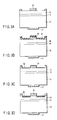
- FIGS. 2A to 2 D are cross-sectional views each illustrating the state of finely recessed/projected portions according to one embodiment of the present invention
- FIGS. 3A to 3 D are cross-sectional views each illustrating, stepwise, the manufacturing steps of an LED according to one embodiment of the present invention.
- FIGS. 4A to 4 D are cross-sectional views each illustrating, stepwise, the manufacturing steps of an LED according to another embodiment of the present invention.
- FIGS. 5A and 5B are cross-sectional views each illustrating the element structure of an LED according to a further embodiment of the present invention.
- FIGS. 6A and 6B are cross-sectional views each illustrating the element structure of an LED according to a further embodiment of the present invention.
- FIG. 7 is a cross-sectional view illustrating the element structure of an LED according to a further embodiment of the present invention.
- FIGS. 8A to 8 C are cross-sectional views each illustrating, stepwise, the manufacturing steps of an LED according to a further embodiment of the present invention.
- FIGS. 9A to 9 C are cross-sectional views each illustrating, stepwise, the manufacturing steps of an LED according to a further embodiment of the present invention.
- FIG. 10 is a microphotograph illustrating the features of the recessed/projected surface according to one embodiment of the present invention.
- FIGS. 11A to 11 C are cross-sectional views each illustrating, stepwise, the manufacturing steps of an LED according to a further embodiment of the present invention.
- FIG. 1 is a cross-sectional view illustrating the element structure of an LED according to a first embodiment of the present invention.
- an n-type GaP substrate 10 on the top surface (the first surface) of an n-type GaP substrate 10 are deposited semiconductor laminated layers comprising a hetero structure portion 14 which is constituted by an n-type InAlP clad layer 11 , an InGaAlP activated layer 12 and a p-type InAlP clad layer 13 ; and a p-type GaP current diffusion layer 15 .
- a p-side electrode (upper electrode) 16 is formed on part of the surface of the current diffusion layer 15 with the remaining portion of the surface of the current diffusion layer 15 being left exposed.
- an n-side electrode (lower electrode) 17 is formed on the bottom surface (the second surface) of the substrate 10 .
- the light emitted from the activated layer 12 is taken up from the exposed surface of the current diffusion layer 15 . Namely, the exposed surface of the current diffusion layer 15 is employed as a light-extracting surface.
- finely recessed/projected portions 18 are formed by a diblock copolymer as explained hereinafter, and configured as shown in FIG. 2A , for instance.
- “h” is the height of the projected portion of the recessed/projected portions 18
- “d” is the length (width) of the base of the projected portion.
- This projected portion is triangular in cross section with the width of the base thereof (d) ranging from 10 to 500 nm, the height thereof (h) being 100 nm or more, and the apex angle thereof ranging from 25 to 80 degrees, these numerical limitations being admitted as effective in securing a sufficient effect to improve the light extraction efficiency.
- the non-uniformity in configuration of the projected portion within the element was found, for example, 100 ⁇ 50 nm in width and 200 ⁇ 100 nm in height (i.e. the distribution of width within the element: ⁇ 50%, and the distribution of height within the element: ⁇ 50%).
- At least part of the recessed/projected portions 18 may be constructed such that the tip end of the projected portion is provided with a fine transparent portion as shown in FIG. 2 B.
- the tip end of the projected portion may be flattened as shown in FIG. 2 C.
- the tip end of the projected portion may be flattened and provided thereon with a fine transparent portion as shown in FIG. 2 D.
- the hetero structure portion 14 and the current diffusion layer 15 were successively epitaxially grown on the top surface of the n-type GaP substrate 10 . Then, the p-side electrode 16 was formed on a desired region of the surface of the current diffusion layer 15 , and the n-side electrode 17 was formed on the bottom surface of the substrate 10 .
- a 1:2.5 diblock copolymer comprising polystyrene (PS) and poly(methyl methacrylate)(PMMA) was dissolved in a solvent formed of ethylcellosolve acetate (ECA) to prepare a solution of the copolymer.
- ECA ethylcellosolve acetate
- a 1:2-3 diblock copolymer comprising PS and PMMA may be used, and it is possible to use propylene glycol monomethyl ether acetate (PGMEA) or ethyl lactate (EL) as a solvent.
- PMEA propylene glycol monomethyl ether acetate
- EL ethyl lactate
- This solution was then spin-coated over the current diffusion layer 15 and the p-side electrode 16 at a rotational speed of 2500 rpm to form a coated film, which was then pre-baked at a temperature of 110° C. for 90 seconds to volatilize the solvent to form a polymer layer 31 as shown in FIG. 3 B. Thereafter, the polymer layer 31 was subjected to annealing in a nitrogen gas atmosphere at a temperature of 210° C. for 4 hours to permit the diblock copolymer to take place the phase separation thereof into PS and PMMA.
- the polymer layer containing this phase-separated diblock copolymer was then subjected to etching by RIE using CF 4 (30 sccm) under the conditions of 1.33 Pa in pressure and 100 W in power output.
- RIE reactive ion etching
- CF 4 CF 4
- This PS pattern 32 was subsequently employed as a mask material layer. More specifically, this PS pattern 32 was transcribed onto the surface of the current diffusion layer 15 by RIE using BCl 3 (23 sccm) and N 2 (7 sccm).
- This transcription was performed for about 100 seconds under the conditions of: 0.2 Pa in pressure, and 500 W in power output. As a result, it was possible to form a finely recessed/projected pattern on the surface of the current diffusion layer 15 as shown in FIG. 3 D.
- the aforementioned RIE may be performed by using BCl 3 (8 sccm), Cl 2 (5 sccm) and Ar (37 sccm) with other conditions being the same as described above. Thereafter, the remaining PS pattern was removed by an O 2 asher to obtain a structure as shown in FIG. 1 .
- the projected portion of the recessed/projected portions was about 100 ⁇ 50 nm in base length, about 200 ⁇ 100 nm in height and 20 to 40 degrees in apex angle. Due to the existence of these finely recessed/projected portions, it is now possible to take up light out of the current diffusion layer 15 even if the incidence angle at the light-extracting surface is increased. Further, even if the light-extracting surface is sealed with a transparent resin, it is possible to improve the light extraction efficiency.
- the diblock copolymer having a polymer chain which is capable of exhibiting a sufficiently large difference in dry etching rate it is possible to employ a diblock copolymer having an aromatic ring-containing polymer chain and an acrylic polymer chain.
- the aromatic ring-containing polymer chain it is possible to employ a polymer chain which can be synthesized through the polymerization of at least one monomer selected from the group consisting of vinyl naphthalene, styrene and derivatives thereof.
- the acrylic polymer chain it is possible to employ a polymer chain which can be obtained through the polymerization of at least one monomer selected from the group consisting of acrylic acid, methacrylic acid, crotonic acid, and derivatives thereof.
- a typical example of the diblock copolymer is a 1:2.5 diblock copolymer comprising polystyrene and poly(methyl methacrylate), which was employed in this embodiment.
- the finely recessed/projected portions can be uniformly created on the light-extracting surface, it is now possible to prevent the degrading of the light extraction efficiency that may be caused due to the influence by the total reflection of light. As a result, it is now possible to enhance the light extraction efficiency and hence to enhance the luminance of LED.
- the method of this embodiment enables to form finely recessed/projected portions in a very efficient manner irrespective of the orientation of the crystal plane of substrate.
- a PS pattern was formed by RIE under the same conditions as described in the aforementioned first embodiment except that O 2 was substituted for CF 4 .
- a polymer layer 31 containing a diblock copolymer was formed on the surface of the current diffusion layer 15 and then, the diblock copolymer was subjected to phase separation. Then, the polymer layer 31 was subjected to etching by RIE using O 2 gas (30 sccm) under the conditions of 13.3 Pa in pressure and 100 W in power output. In contrast with the etching using CF 4 , although it was impossible, in this case where O 2 was employed, to etch the polymer layer 31 down to the underlying substrate, it was possible to relatively accurately remove the PMMA phase of the PS-PMMA block, thereby forming a PS pattern.
- This PS pattern was then transcribed onto the surface of the current diffusion layer 15 by RIE under the same conditions as described in the aforementioned first embodiment except that Cl 2 (5 to 40 sccm) was employed as an etching gas. Thereafter, the PS pattern left remained was removed by using an O 2 asher.
- a PS pattern was formed through the scission of the main chain of polymer by the irradiation of electron beam.
- a polymer layer 31 containing a diblock copolymer was formed on the surface of the current diffusion layer 15 and then, the diblock copolymer was subjected to phase separation. Then, an electron beam was irradiated the entire surface of the polymer layer 31 to cut the main chain of PMMA. On this occasion, the conditions of irradiating the electron beam were set to 2 eV. Thereafter, the polymer layer 31 was subjected to development by using a developing solution (for example, a mixed solution comprising MIBK (methylisobutyl ketone) and IPA(isopropanol)). The resultant surface of the polymer layer 31 was then rinsed by IPA or ethanol to selectively dissolve and remove the PMMA, thereby leaving a pattern 32 of PS.
- a developing solution for example, a mixed solution comprising MIBK (methylisobutyl ketone) and IPA(isopropanol)
- This PS pattern was then transcribed onto the surface of the current diffusion layer 15 by RIE under the same conditions as described in the aforementioned first embodiment except that Cl 2 (5 to 40 sccm) was employed as an etching gas. Thereafter, the PS pattern left remained was removed by using an O 2 asher.
- a material containing an aromatic ring-containing polymer chain and an aliphatic double-bond polymer chain was employed as a diblock copolymer.
- This aliphatic double-bond polymer is a polymer containing a double-bond in the main chain of the polymer, wherein the double-bond is cut off by the effect of oxidation using ozone for instance. Therefore, it is possible, in the case of a diblock copolymer containing an aromatic ring-containing polymer chain and an aliphatic double-bond polymer chain, to selectively remove the aliphatic double-bond polymer chain.
- specific examples of the aliphatic double-bond polymer chain it is possible to employ polydiene-based polymer and derivatives thereof.
- diblock copolymer containing an aromatic ring-containing polymer chain and an aliphatic double-bond polymer chain it is possible to employ a diblock copolymer comprising polystyrene and polybutadiene, a diblock copolymer comprising polystyrene and polyisoprene, etc.
- a 1:2.5 diblock copolymer comprising polystyrene (PS)-polyisoprene was employed to form a polymer layer on the current diffusion layer 15 in the same manner as described in the first embodiment, and then, the diblock copolymer was subjected to phase separation. Subsequently, this phase-separated diblock copolymer was left to stand in an ozone atmosphere for 5 minutes, thereby removing the polyisoprene, thus forming a pattern of PS. Thereafter, by the same procedures as described in the aforementioned first embodiment, the pattern of PS was transcribed onto the surface of the current diffusion layer 15 .
- PS polystyrene
- FIGS. 4A to 4 D are cross-sectional views each illustrating, stepwise, the manufacturing steps of an LED according to a fifth embodiment of the present invention. Incidentally, the same portions as those of FIGS. 3A to 3 D will be identified by the same reference numbers in FIGS. 4A to 4 D, thereby omitting the detailed explanation thereof.
- the finely recessed/projected portions were formed on the surface of a transparent layer formed on the current diffusion layer.
- a transparent film 41 was formed on the surface of the current diffusion layer 15 .
- This transparent film 41 can be formed, for example, by a sputtering method, a CVD method or a coating method by SiO 2 , SiN 2 , TiO 2 , etc.
- a polymer film 31 was formed on the transparent film 41 . Thereafter, the polymer film 31 was subjected to annealing in a nitrogen atmosphere at a temperature of 210° C. for 4 hours to permit the diblock copolymer to take place the phase separation thereof.
- the polymer layer containing this phase-separated diblock copolymer was then subjected to etching by RIE to form a pattern 32 of PS, which was subsequently transcribed onto the surface of the transparent film 41 as shown in FIG. 4 C.
- the RIE in this case can be performed using an etching gas such as CF 4 , CHF 3 , C 4 F 8 , SF 6 , etc. and under the conditions of: 5-10 Pa in pressure, and 100-1000 W in power output.
- the PS pattern remaining was removed by using an O 2 asher to form finely recessed/projected portions on the surface of the transparent film 41 as shown in FIG. 4 D.
- These finely recessed/projected portions were found excellent in uniformity as those of the first embodiment with the projected portion thereof being about 100 ⁇ 50 nm in base length, about 200 ⁇ 100 nm in height.
- the finely recessed/projected portions formed in the transparent film 41 may be transcribed onto the current diffusion layer 15 subsequent to the formation of the structure shown in FIG. 4D , and then, the transparent film 41 may be removed by a chemical solution such as HF, NH 4 F, etc.
- the finely recessed/projected portions can be formed on the surface of the current diffusion layer 15 in the same manner as described in the first embodiment.
- FIGS. 5A and 5B are cross-sectional views each illustrating the element structure of an LED according to a sixth embodiment of the present invention.
- the LED shown in FIG. 5A is a Junction Up type LED where the light is extracted from a surface located opposite to the substrate 50 .
- an n-type GaN buffering layer 51 an n-type GaN clad layer 52 , an MQW activated layer 53 containing InGaN/GaN, a p-type AlGaN cap layer 54 , and a p-type GaN contact layer 55 are successively deposited on the surface of an n-type GaN substrate 50 .
- a p-side electrode 57 is formed on part of the surface of the contact layer 55 with the remaining portion of the surface of the contact layer 55 being left exposed.
- an n-side electrode 58 is formed on the bottom surface of the substrate 50 .
- Finely recessed/projected portions 55 a are formed on the exposed surface of the contact layer 55 by the same procedures as explained above.
- the finely recessed/projected portions may be formed in the dielectric film which is disposed on the exposed surface of the contact layer 55 .
- these finely recessed/projected portions 55 a can be uniformly formed on the surface of the light-extracting surface, it is possible to enhance the light extraction efficiency.
- the LED shown in FIG. 5B is a Junction Down type LED where the light is extracted from the substrate 50 side.
- the same kinds of layers as those of FIG. 5A i.e. the layers 51 , 52 , 53 , 54 and 55 are successively deposited on the surface of an n-type GaP substrate 50 .
- a p-side electrode 57 is formed on the surface of the contact layer 55
- an n-side electrode 58 which has been patterned is formed partially on the bottom surface of the substrate 50 .
- the remaining region of the bottom surface of the substrate 50 is left exposed and provided with finely recessed/projected portions 50 a which have been formed by the same procedures as explained above.
- these finely recessed/projected portions 50 a can be uniformly formed on the bottom surface of the substrate 50 functioning as a light-extracting surface, it is possible to enhance the light extraction efficiency.
- the light emitted from the MQW activated layer 53 is reflected by each of the end faces, thus enabling the light to be extracted from the finely recessed/projected portions 50 a which are formed on the top surface of the substrate, thereby making it possible to minimize the density of light at the sidewall of chip.
- FIGS. 6A and 6B are cross-sectional views each illustrating the element structure of an LED according to a seventh embodiment of the present invention.
- the LED shown in FIG. 6A is a Junction Up type LED where the light is extracted from a surface located opposite to the substrate 60 .
- an AlGaN buffering layer 61 an n-type GaN contact layer 62 , an MQW activated layer 63 containing InGaN/GaN, a p-type AlGaN cap layer 64 , a p-type GaN contact layer 65 and a transparent electrode 66 made of ITO for instance are successively deposited on the top surface of a sapphire substrate 60 .
- This laminate is partially etched in such a manner that the etched region is extended from the transparent electrode 66 down to an intermediate portion of the n-type GaN contact layer 62 .
- a p-side electrode 67 is formed on part of the surface of the transparent electrode 66 with the remaining portion of the surface of the transparent electrode 66 being left exposed.
- On the exposed surface of the contact layer 62 there is formed an n-side electrode 68 . Finely recessed/projected portions 66 a are formed on the exposed surface of the transparent electrode 66 by using the same procedures as explained above.
- these finely recessed/projected portions 66 a can be uniformly formed on the surface of the transparent electrode 66 constituting a light-extracting surface, it is possible to enhance the light extraction efficiency.
- the LED shown in FIG. 6B is a Junction Down type LED where the light is extracted from the substrate 60 side.
- the same kinds of layers as those of FIG. 6A i.e. the layers 61 , 62 , 63 , 64 and 65 are successively deposited on the surface of a sapphire substrate 60 .
- This laminate is partially etched in such a manner that the etched region is extended from the p-type contact layer 65 up to an intermediate portion of the n-type contact layer 62 .
- a p-side electrode 67 is formed on the surface of the p-type contact layer 65
- an n-side electrode 68 is formed on the exposed surface of the n-type contact layer 62 .
- Finely recessed/projected portions 60 a are formed the entire surface of the substrate 60 by using the same procedures as explained above.
- these finely recessed/projected portions 60 a can be uniformly formed on the bottom surface of the substrate 60 functioning as a light-extracting surface, it is possible to enhance the light extraction efficiency.
- FIG. 7 is a cross-sectional view illustrating the element structure of an LED according to an eighth embodiment of the present invention.
- a p-type GaP buffering layer 71 a p-type InGaP adhesion layer 72 , a p-type InAlP clad layer 73 , an InGaAlP activated layer 74 , an n-type InAlP clad layer 75 and an n-type InGaAlP current diffusion layer 76 are successively deposited on the surface of a p-type GaP substrate 70 .
- On the peripheral region of the surface of the current diffusion layer 76 there are deposited the n-type GaAs contact layer 77 and the n-side electrode 81 .
- a p-side electrode 82 which has been patterned is formed on the bottom surface of the substrate 70 . Finely recessed/projected portions 83 are formed on the exposed surface of the current diffusion layer 75 by the same procedures as explained above.
- an n-type GaAs buffering layer 91 (0.5 ⁇ m in thickness; 4 ⁇ 10 17 cm ⁇ 3 in carrier concentration), an i-type InGaP etch-stop layer 92 (0.2 ⁇ m), an i-type GaAs block cover layer 79 (0.1 ⁇ m), an i-type InAlP block layer 78 (0.2 ⁇ m), an n-type GaAs contact layer 77 (0.1 ⁇ m in thickness; 1 ⁇ 10 18 cm ⁇ 3 in carrier concentration), an n-type InGaAlP current diffusion layer 76 (1.5 ⁇ m in thickness; 4 ⁇ 10 17 cm ⁇ 3 in carrier concentration), an n-type InAlP clad layer 75 (0.6 ⁇ m in thickness; 4 ⁇ 10 17 cm ⁇ 3 in carrier concentration), an InGaAlP-MQW activated layer 74 (0.72 ⁇ m in thickness; 621 nm in wavelength), a p-type InAlP clad layer
- a p-type GaP layer 71 (0.2 ⁇ m in thickness; 3 ⁇ 10 18 cm ⁇ 3 in carrier concentration) was allowed to grow on the surface of a p-type GaP substrate 70 having a thickness of 150 ⁇ m to prepare a supporting substrate. Then, this supporting substrate was adhered onto the adhesion layer 72 . Thereafter, the GaAs substrate 90 , the buffering layer 91 and the etch-stop layer 92 were etched away to obtain a structure as shown in FIG. 8 B.
- the block cover layer 79 , the block layer 78 and the contact layer 77 were etched so as to form a pattern of electrode.
- the central portion of these layers was patterned into a circular configuration, and the peripheral portion thereof was formed into a pattern of fine linear configuration, and at the same time, the block cover layer 79 and the block layer 78 were removed.
- an n-side electrode 81 was formed on the uppermost layer thereof, while a p-side electrode 82 was formed on the bottom surface of the substrate 70 .
- the p-side electrode 82 was formed as a circular pattern at four locations of the substrate excluding the central region of the substrate in order to enhance the light extraction efficiency of the region immediately below the portion where the n-side electrode 81 was not located. This p-side electrode 82 can be formed all over the bottom surface of the substrate 70 .
- these finely recessed/projected portions 83 can be uniformly formed the entire surface of the current diffusion layer 76 functioning as a light-extracting surface except the region where the electrode 81 was formed, it is possible to enhance the light extraction efficiency.
- an SOG film 93 having a thickness of 0.1 ⁇ m and comprising an SiO 2 film was formed on the surface of the InGaAlP current diffusion layer 76 of the laminate structure shown in FIG. 7 by a spin-coating method. Then, a polymer film containing a diblock copolymer was formed on the surface of the SOG film 93 in the same manner as described in the first embodiment, and the polymer layer was allowed to take place the phase separation thereof.
- phase-separated polymer film was subjected to etching for 30 seconds by RIE using O 2 gas (30 sccm) under the conditions of 13 Pa in pressure and 100 W in power output, thereby forming a polymer pattern 94 .
- This polymer pattern 94 was then employed as a mask to etch the SOG film 93 for about 100 seconds by RIE using CF 4 gas (30 sccm) under the conditions of 1.3 Pa in pressure and 100 W in power output, thereby forming a pattern of SOG as shown in FIG. 9 B.
- the resultant surface was subjected to etching for about 100 seconds by RIE using BCl 3 (8 sccm), Cl 2 (5 sccm) and Ar (37 sccm) under the conditions of: 0.2 Pa in pressure, and 500 W in power output.
- RIE reactive ion etching
- FIG. 9C it was possible, as shown in FIG. 9C , to form finely recessed/projected portions 83 with the projected portion having a minute cone-like configuration 50-300 nm in width and 100-500 nm in height on the surface of the InGaAlP current diffusion layer 76 .
- the SOG (oxide film) 93 may be left at the apex portion of the finely recessed/projected portions, i.e. no trouble would be raised even if the SOG is left in this manner.
- FIG. 10 shows an electron microphotograph of the finely recessed/projected portions.
- FIGS. 11A to 11 C A method of working an underlying substrate by using a multi-layer resist system will be explained with reference to FIGS. 11A to 11 C.
- an underlying resist film (positive novolac resist) 95 having a thickness of 0.1 ⁇ m was formed on the surface of the InGaAlP current diffusion layer 76 .
- the resist to be employed in this case may not contain a photosensitive agent.
- an SOG film 93 and a polymer film were formed on the surface of the underlying resist film 95 in the same manner as described above.
- phase-separated polymer film was subjected to etching for 30 seconds by RIE using O 2 gas (30 sccm) under the conditions of 13 Pa in pressure and 100 W in power output, thereby forming a polymer pattern 94 .
- This polymer pattern 94 was then employed as a mask to etch the SOG film 93 by RIE, and the underlying resist film 95 was etched by RIE using O 2 gas (8 sccm) and N 2 gas (80 sccm) under the conditions of 2 Pa in pressure and 300 W in power output, thereby forming a resist pattern 95 a as shown in FIG. 11 B.
- a resist pattern 95 a was peeled off by using an O 2 asher, thereby forming, as shown in FIG. 11C , finely recessed/projected portions 83 on the surface of the InGaAlP current diffusion layer 76 , each projected portion thereof having a cone-like configuration about 50-200 nm in width and 100-500 nm in height.
- each projected portion having a cone-like configuration 100 ⁇ 50 nm in base length and 300 ⁇ 150 nm in height.
- the finely recessed/projected portions that have been defined as mentioned above are formed on the light-extracting surface, it is now possible to prevent the degrading of the light extraction efficiency that may be caused due to the influence by the total reflection of light. As a result, it is now possible to enhance the light extraction efficiency. Furthermore, it is now possible to minimize the internal absorption loss that may be caused by the multi-reflection in the interior of the semiconductor layer, thereby making it possible to realize a light-emitting element capable of extremely minimizing temperature increase. Additionally, since the surface-roughening treatment using a diblock copolymer is applied to the light-extracting surface, it is now possible to uniformly form finely recessed/projected portions without depending on the crystal orientation of the underlying layer.
- the present invention should not be construed as being limited to the aforementioned embodiments.
- the materials for forming the polymer layer it is possible to employ any diblock copolymer as long as they are capable of selectively removing one of the components that have been phase-separated.
- the finely recessed/projected portions can be formed on any desired layer as long as it is located at an uppermost layer of the light-extracting side and at the same time, capable of being worked through etching using a phase-separated polymer film as a mask.
- the projected portion of the finely recessed/projected portions is formed of a cone-like configuration, it is possible to obtain the advantages as mentioned above.
- the finely recessed/projected portions having a cone-like configuration may be formed on each of the surfaces (top and side surfaces) of the chip other than the portions where electrodes are formed. The aforementioned advantages would not be hindered even if the electrodes are formed after the finely recessed/projected portions have been formed all over the light-extracting surface.
- the present invention can be executed by modifying it in various ways as long as such variations do not exceed the subject matter of the present invention.
Abstract
Description
Claims (12)
Priority Applications (1)
| Application Number | Priority Date | Filing Date | Title |
|---|---|---|---|
| US11/054,409 US20050145864A1 (en) | 2002-01-18 | 2005-02-10 | Semiconductor light-emitting element and method of manufacturing the same |
Applications Claiming Priority (2)
| Application Number | Priority Date | Filing Date | Title |
|---|---|---|---|
| JP2002010571A JP3782357B2 (en) | 2002-01-18 | 2002-01-18 | Manufacturing method of semiconductor light emitting device |
| JP2002-010571 | 2002-01-18 |
Related Child Applications (1)
| Application Number | Title | Priority Date | Filing Date |
|---|---|---|---|
| US11/054,409 Division US20050145864A1 (en) | 2002-01-18 | 2005-02-10 | Semiconductor light-emitting element and method of manufacturing the same |
Publications (2)
| Publication Number | Publication Date |
|---|---|
| US20030178626A1 US20030178626A1 (en) | 2003-09-25 |
| US7037738B2 true US7037738B2 (en) | 2006-05-02 |
Family
ID=19191603
Family Applications (2)
| Application Number | Title | Priority Date | Filing Date |
|---|---|---|---|
| US10/346,108 Expired - Fee Related US7037738B2 (en) | 2002-01-18 | 2003-01-17 | Method of manufacturing a semiconductor light-emitting element |
| US11/054,409 Abandoned US20050145864A1 (en) | 2002-01-18 | 2005-02-10 | Semiconductor light-emitting element and method of manufacturing the same |
Family Applications After (1)
| Application Number | Title | Priority Date | Filing Date |
|---|---|---|---|
| US11/054,409 Abandoned US20050145864A1 (en) | 2002-01-18 | 2005-02-10 | Semiconductor light-emitting element and method of manufacturing the same |
Country Status (5)
| Country | Link |
|---|---|
| US (2) | US7037738B2 (en) |
| EP (1) | EP1329961A3 (en) |
| JP (1) | JP3782357B2 (en) |
| CN (1) | CN1229877C (en) |
| TW (1) | TW575984B (en) |
Cited By (67)
| Publication number | Priority date | Publication date | Assignee | Title |
|---|---|---|---|---|
| US20040227446A1 (en) * | 2003-02-26 | 2004-11-18 | Akira Fujimoto | Display device and method of manufacturing transparent substrate for display device |
| US20060011934A1 (en) * | 2003-10-03 | 2006-01-19 | Dowa Mining Co., Ltd. | Semiconductor light-emitting element and manufacturing method thereof |
| US20060183348A1 (en) * | 2005-02-17 | 2006-08-17 | Meagley Robert P | Layered films formed by controlled phase segregation |
| US20060231525A1 (en) * | 1999-06-07 | 2006-10-19 | Koji Asakawa | Method for manufacturing porous structure and method for forming pattern |
| US20070018183A1 (en) * | 2005-07-21 | 2007-01-25 | Cree, Inc. | Roughened high refractive index layer/LED for high light extraction |
| US20070210327A1 (en) * | 2006-03-07 | 2007-09-13 | Shin-Etsu Handotai Co., Ltd. | Method of fabricating light emitting device and thus-fabricated light emitting device |
| US20070224714A1 (en) * | 2004-04-27 | 2007-09-27 | Shin-Etsu Handotai Co., Ltd. | Method of Fabricating Light Emitting Device and Thus-Fabricated Light Emitting Device |
| US20070243653A1 (en) * | 2006-03-30 | 2007-10-18 | Crystal Is, Inc. | Methods for controllable doping of aluminum nitride bulk crystals |
| US20080061307A1 (en) * | 2004-04-27 | 2008-03-13 | Shin-Etsu Handotai Co., Ltd. | Method of Fabricating Light Emitting Device and Thus-Fabricated Light Emitting Device |
| US20080121910A1 (en) * | 2006-11-28 | 2008-05-29 | Michael John Bergmann | Semiconductor Devices Having Low Threading Dislocations and Improved Light Extraction and Methods of Making the Same |
| US20080182092A1 (en) * | 2007-01-17 | 2008-07-31 | Crystal Is, Inc. | Defect reduction in seeded aluminum nitride crystal growth |
| US20080187016A1 (en) * | 2007-01-26 | 2008-08-07 | Schowalter Leo J | Thick Pseudomorphic Nitride Epitaxial Layers |
| US20080199653A1 (en) * | 2007-02-15 | 2008-08-21 | Hong Kong Applied Science And Technology Research Institute Co. Ltd. | Method of forming two-dimensional pattern by using nanospheres |
| US20080257187A1 (en) * | 2007-04-18 | 2008-10-23 | Micron Technology, Inc. | Methods of forming a stamp, methods of patterning a substrate, and a stamp and a patterning system for same |
| US20080315270A1 (en) * | 2007-06-21 | 2008-12-25 | Micron Technology, Inc. | Multilayer antireflection coatings, structures and devices including the same and methods of making the same |
| US20090028202A1 (en) * | 2005-08-01 | 2009-01-29 | Hwan Hee Jeong | Nitride light emitting device and manufacturing method thereof |
| US20090050050A1 (en) * | 2007-05-24 | 2009-02-26 | Crystal Is, Inc. | Deep-eutectic melt growth of nitride crystals |
| US7582910B2 (en) | 2005-02-28 | 2009-09-01 | The Regents Of The University Of California | High efficiency light emitting diode (LED) with optimized photonic crystal extractor |
| US20090275154A1 (en) * | 2005-05-31 | 2009-11-05 | Shin-Etsu Handotai Co., Ltd. | Method of fabricating light emitting device |
| US20100065868A1 (en) * | 2008-09-12 | 2010-03-18 | Kabushiki Kaisha Toshiba | Semiconductor light emitting device |
| US20100102415A1 (en) * | 2008-10-28 | 2010-04-29 | Micron Technology, Inc. | Methods for selective permeation of self-assembled block copolymers with metal oxides, methods for forming metal oxide structures, and semiconductor structures including same |
| US20100187541A1 (en) * | 2005-12-02 | 2010-07-29 | Crystal Is, Inc. | Doped Aluminum Nitride Crystals and Methods of Making Them |
| US20100221856A1 (en) * | 2009-01-06 | 2010-09-02 | Akira Fujimoto | Semiconductor light-emitting device and process for production thereof |
| US20100220757A1 (en) * | 2009-02-18 | 2010-09-02 | Ryota Kitagawa | Semiconductor light-emitting element and process for production thereof |
| US20100264460A1 (en) * | 2007-01-26 | 2010-10-21 | Grandusky James R | Thick pseudomorphic nitride epitaxial layers |
| US20100314551A1 (en) * | 2009-06-11 | 2010-12-16 | Bettles Timothy J | In-line Fluid Treatment by UV Radiation |
| US20110008621A1 (en) * | 2006-03-30 | 2011-01-13 | Schujman Sandra B | Aluminum nitride bulk crystals having high transparency to ultraviolet light and methods of forming them |
| US20110011332A1 (en) * | 2001-12-24 | 2011-01-20 | Crystal Is, Inc. | Method and apparatus for producing large, single-crystals of aluminum nitride |
| US20110033965A1 (en) * | 2006-08-21 | 2011-02-10 | Samsung Led Co., Ltd. | Vertical nitride semiconductor light emitting diode and method of manufacturing the same |
| US20110095306A1 (en) * | 2009-10-22 | 2011-04-28 | Sung Min Hwang | Light emitting device, light emitting device package and lighting system |
| US20110169041A1 (en) * | 2008-01-11 | 2011-07-14 | Lg Innotek Co., Ltd. | Light emitting device |
| US20110227037A1 (en) * | 2010-03-12 | 2011-09-22 | Applied Materials, Inc. | Enhancement of led light extraction with in-situ surface roughening |
| US20110297982A1 (en) * | 2008-08-29 | 2011-12-08 | Norbert Linder | Optoelectronic Semiconductor Chip |
| US8097891B2 (en) | 2006-02-16 | 2012-01-17 | Sumitomo Chemical Company, Limited | Group III nitride semiconductor light emitting device and method for producing the same |
| US20120025246A1 (en) * | 2010-07-02 | 2012-02-02 | Tae Hun Kim | Semiconductor light emitting device and method of manufacturing the same |
| US20120032306A1 (en) * | 2009-02-10 | 2012-02-09 | Osram Opto Semiconductors Gmbh | Method for Patterning a Semiconductor Surface, and Semiconductor Chip |
| US8557128B2 (en) | 2007-03-22 | 2013-10-15 | Micron Technology, Inc. | Sub-10 nm line features via rapid graphoepitaxial self-assembly of amphiphilic monolayers |
| US20130292731A1 (en) * | 2006-10-17 | 2013-11-07 | Epistar Corporation | Light-emitting device |
| US8609221B2 (en) | 2007-06-12 | 2013-12-17 | Micron Technology, Inc. | Alternating self-assembling morphologies of diblock copolymers controlled by variations in surfaces |
| US8633112B2 (en) | 2008-03-21 | 2014-01-21 | Micron Technology, Inc. | Thermal anneal of block copolymer films with top interface constrained to wet both blocks with equal preference |
| US8642157B2 (en) | 2008-02-13 | 2014-02-04 | Micron Technology, Inc. | One-dimensional arrays of block copolymer cylinders and applications thereof |
| US8641914B2 (en) | 2008-03-21 | 2014-02-04 | Micron Technology, Inc. | Methods of improving long range order in self-assembly of block copolymer films with ionic liquids |
| US8753738B2 (en) | 2007-03-06 | 2014-06-17 | Micron Technology, Inc. | Registered structure formation via the application of directed thermal energy to diblock copolymer films |
| US8785559B2 (en) | 2007-06-19 | 2014-07-22 | Micron Technology, Inc. | Crosslinkable graft polymer non-preferentially wetted by polystyrene and polyethylene oxide |
| TWI450419B (en) * | 2011-12-03 | 2014-08-21 | Hon Hai Prec Ind Co Ltd | Light emitting diode |
| TWI452728B (en) * | 2011-12-03 | 2014-09-11 | Hon Hai Prec Ind Co Ltd | Light emitting diode |
| US8858004B2 (en) | 2005-12-22 | 2014-10-14 | Cree, Inc. | Lighting device |
| US8900963B2 (en) | 2011-11-02 | 2014-12-02 | Micron Technology, Inc. | Methods of forming semiconductor device structures, and related structures |
| US8962359B2 (en) | 2011-07-19 | 2015-02-24 | Crystal Is, Inc. | Photon extraction from nitride ultraviolet light-emitting devices |
| US8981342B2 (en) | 2011-12-03 | 2015-03-17 | Tsinghua University | Light emitting diode with three-dimensional nano-structures on a semiconductor layer and an active layer |
| US8993088B2 (en) | 2008-05-02 | 2015-03-31 | Micron Technology, Inc. | Polymeric materials in self-assembled arrays and semiconductor structures comprising polymeric materials |
| US8999492B2 (en) | 2008-02-05 | 2015-04-07 | Micron Technology, Inc. | Method to produce nanometer-sized features with directed assembly of block copolymers |
| US9028612B2 (en) | 2010-06-30 | 2015-05-12 | Crystal Is, Inc. | Growth of large aluminum nitride single crystals with thermal-gradient control |
| US9087699B2 (en) | 2012-10-05 | 2015-07-21 | Micron Technology, Inc. | Methods of forming an array of openings in a substrate, and related methods of forming a semiconductor device structure |
| TWI497759B (en) * | 2011-05-31 | 2015-08-21 | ||
| US9142420B2 (en) | 2007-04-20 | 2015-09-22 | Micron Technology, Inc. | Extensions of self-assembled structures to increased dimensions via a “bootstrap” self-templating method |
| US9177795B2 (en) | 2013-09-27 | 2015-11-03 | Micron Technology, Inc. | Methods of forming nanostructures including metal oxides |
| TWI511328B (en) * | 2012-06-20 | 2015-12-01 | Just Innovation Corp | Light-emitting diode chip and manufacturing method thereof |
| TWI513030B (en) * | 2010-06-01 | 2015-12-11 | Advanced Optoelectronic Tech | Light-emitting diode and method for manufacturing the same |
| US9229328B2 (en) | 2013-05-02 | 2016-01-05 | Micron Technology, Inc. | Methods of forming semiconductor device structures, and related semiconductor device structures |
| US9299880B2 (en) | 2013-03-15 | 2016-03-29 | Crystal Is, Inc. | Pseudomorphic electronic and optoelectronic devices having planar contacts |
| US9447521B2 (en) | 2001-12-24 | 2016-09-20 | Crystal Is, Inc. | Method and apparatus for producing large, single-crystals of aluminum nitride |
| US20170098735A1 (en) * | 2015-10-02 | 2017-04-06 | Epistar Corporation | Light-emitting device |
| US9771666B2 (en) | 2007-01-17 | 2017-09-26 | Crystal Is, Inc. | Defect reduction in seeded aluminum nitride crystal growth |
| US9847232B1 (en) | 2017-03-24 | 2017-12-19 | Jsr Corporation | Pattern-forming method |
| US11370872B2 (en) | 2016-07-07 | 2022-06-28 | Jsr Corporation | Composition for pattern formation, and pattern-forming method |
| US11460767B2 (en) | 2016-07-06 | 2022-10-04 | Jsr Corporation | Composition for film formation, film-forming method and directed self-assembly lithography process |
Families Citing this family (173)
| Publication number | Priority date | Publication date | Assignee | Title |
|---|---|---|---|---|
| DE10234977A1 (en) * | 2002-07-31 | 2004-02-12 | Osram Opto Semiconductors Gmbh | Radiation-emitting thin layer semiconductor component comprises a multiple layer structure based on gallium nitride containing an active radiation-producing layer and having a first main surface and a second main surface |
| US7521854B2 (en) * | 2003-04-15 | 2009-04-21 | Luminus Devices, Inc. | Patterned light emitting devices and extraction efficiencies related to the same |
| US7098589B2 (en) | 2003-04-15 | 2006-08-29 | Luminus Devices, Inc. | Light emitting devices with high light collimation |
| US7211831B2 (en) * | 2003-04-15 | 2007-05-01 | Luminus Devices, Inc. | Light emitting device with patterned surfaces |
| EP2264798B1 (en) | 2003-04-30 | 2020-10-14 | Cree, Inc. | High powered light emitter packages with compact optics |
| US7005679B2 (en) | 2003-05-01 | 2006-02-28 | Cree, Inc. | Multiple component solid state white light |
| DE10335080A1 (en) | 2003-07-31 | 2005-03-03 | Osram Opto Semiconductors Gmbh | Method for producing a multiplicity of optoelectronic semiconductor chips and optoelectronic semiconductor chip |
| DE10335081A1 (en) * | 2003-07-31 | 2005-03-03 | Osram Opto Semiconductors Gmbh | Method for producing a multiplicity of optoelectronic semiconductor chips and optoelectronic semiconductor chip |
| GB0318817D0 (en) * | 2003-08-11 | 2003-09-10 | Univ Cambridge Tech | Method of making a polymer device |
| DE10340271B4 (en) * | 2003-08-29 | 2019-01-17 | Osram Opto Semiconductors Gmbh | Thin-film light-emitting diode chip and method for its production |
| EP1668687A4 (en) * | 2003-09-19 | 2007-11-07 | Tinggi Tech Private Ltd | Fabrication of conductive metal layer on semiconductor devices |
| WO2005029573A1 (en) * | 2003-09-19 | 2005-03-31 | Tinggi Technologies Private Limited | Fabrication of semiconductor devices |
| US8604497B2 (en) * | 2003-09-26 | 2013-12-10 | Osram Opto Semiconductors Gmbh | Radiation-emitting thin-film semiconductor chip |
| US7109048B2 (en) | 2003-09-30 | 2006-09-19 | Lg Electronics Inc. | Semiconductor light emitting device and fabrication method thereof |
| US6972438B2 (en) * | 2003-09-30 | 2005-12-06 | Cree, Inc. | Light emitting diode with porous SiC substrate and method for fabricating |
| JP4124102B2 (en) | 2003-11-12 | 2008-07-23 | 松下電工株式会社 | Light emitting device having multiple antireflection structure and method of manufacturing |
| CN100459189C (en) * | 2003-11-19 | 2009-02-04 | 日亚化学工业株式会社 | Semiconductor element and manufacturing method for the same |
| WO2005064666A1 (en) | 2003-12-09 | 2005-07-14 | The Regents Of The University Of California | Highly efficient gallium nitride based light emitting diodes via surface roughening |
| WO2005069388A1 (en) * | 2004-01-20 | 2005-07-28 | Nichia Corporation | Semiconductor light-emitting device |
| JP2005209795A (en) * | 2004-01-21 | 2005-08-04 | Koito Mfg Co Ltd | Light emitting module and lighting tool |
| JP2005251875A (en) * | 2004-03-02 | 2005-09-15 | Toshiba Corp | Semiconductor light emitting device |
| CN100413105C (en) * | 2004-03-05 | 2008-08-20 | 昭和电工株式会社 | Boron phosphide-based semiconductor light-emitting device |
| KR101013724B1 (en) | 2004-03-08 | 2011-02-10 | 엘지전자 주식회사 | Nitride compound light emitting device |
| EP1730790B1 (en) * | 2004-03-15 | 2011-11-09 | Tinggi Technologies Private Limited | Fabrication of semiconductor devices |
| KR100568297B1 (en) * | 2004-03-30 | 2006-04-05 | 삼성전기주식회사 | Nitride semiconductor light emitting device and manufacturing method thereof |
| US7208334B2 (en) * | 2004-03-31 | 2007-04-24 | Kabushiki Kaisha Toshiba | Method of manufacturing semiconductor device, acid etching resistance material and copolymer |
| EP1756875A4 (en) | 2004-04-07 | 2010-12-29 | Tinggi Technologies Private Ltd | Fabrication of reflective layer on semiconductor light emitting diodes |
| JP2005354020A (en) * | 2004-05-10 | 2005-12-22 | Univ Meijo | Semiconductor light-emitting device manufacturing method and semiconductor light-emitting device |
| JP2005327979A (en) * | 2004-05-17 | 2005-11-24 | Toshiba Corp | Semiconductor light-emitting element and device |
| US7768023B2 (en) * | 2005-10-14 | 2010-08-03 | The Regents Of The University Of California | Photonic structures for efficient light extraction and conversion in multi-color light emitting devices |
| US9130119B2 (en) * | 2006-12-11 | 2015-09-08 | The Regents Of The University Of California | Non-polar and semi-polar light emitting devices |
| US7345298B2 (en) * | 2005-02-28 | 2008-03-18 | The Regents Of The University Of California | Horizontal emitting, vertical emitting, beam shaped, distributed feedback (DFB) lasers by growth over a patterned substrate |
| US8227820B2 (en) | 2005-02-09 | 2012-07-24 | The Regents Of The University Of California | Semiconductor light-emitting device |
| US7534633B2 (en) | 2004-07-02 | 2009-05-19 | Cree, Inc. | LED with substrate modifications for enhanced light extraction and method of making same |
| US7375380B2 (en) | 2004-07-12 | 2008-05-20 | Rohm Co., Ltd. | Semiconductor light emitting device |
| JP4635507B2 (en) * | 2004-07-30 | 2011-02-23 | パナソニック電工株式会社 | Method for manufacturing light emitting device |
| KR20070046024A (en) | 2004-08-31 | 2007-05-02 | 각코우호우징 메이조다이가쿠 | Production method for semiconductor light emitting element and semiconductor light emitting element |
| US7476910B2 (en) | 2004-09-10 | 2009-01-13 | Kabushiki Kaisha Toshiba | Semiconductor light emitting device and method for manufacturing the same |
| US7223998B2 (en) * | 2004-09-10 | 2007-05-29 | The Regents Of The University Of California | White, single or multi-color light emitting diodes by recycling guided modes |
| JP4572645B2 (en) * | 2004-09-30 | 2010-11-04 | パナソニック電工株式会社 | Method for manufacturing light emitting device |
| KR100501109B1 (en) * | 2004-12-14 | 2005-07-18 | (주)옵토웨이 | Extensive area led having roughness surface |
| JP2006179511A (en) * | 2004-12-20 | 2006-07-06 | Sumitomo Electric Ind Ltd | Light emitting device |
| US20060267007A1 (en) * | 2004-12-31 | 2006-11-30 | Yale University | Devices incorporating heavily defected semiconductor layers |
| US7473936B2 (en) * | 2005-01-11 | 2009-01-06 | Semileds Corporation | Light emitting diodes (LEDs) with improved light extraction by roughening |
| US7563625B2 (en) * | 2005-01-11 | 2009-07-21 | SemiLEDs Optoelectronics Co., Ltd. | Method of making light-emitting diodes (LEDs) with improved light extraction by roughening |
| US9130114B2 (en) | 2005-01-11 | 2015-09-08 | SemiLEDs Optoelectronics Co., Ltd. | Vertical light emitting diode (VLED) dice having confinement layers with roughened surfaces and methods of fabrication |
| US7186580B2 (en) * | 2005-01-11 | 2007-03-06 | Semileds Corporation | Light emitting diodes (LEDs) with improved light extraction by roughening |
| US7524686B2 (en) * | 2005-01-11 | 2009-04-28 | Semileds Corporation | Method of making light emitting diodes (LEDs) with improved light extraction by roughening |
| US7897420B2 (en) * | 2005-01-11 | 2011-03-01 | SemiLEDs Optoelectronics Co., Ltd. | Light emitting diodes (LEDs) with improved light extraction by roughening |
| JP2006222288A (en) | 2005-02-10 | 2006-08-24 | Toshiba Corp | White led and manufacturing method therefor |
| JP2006261659A (en) * | 2005-02-18 | 2006-09-28 | Sumitomo Chemical Co Ltd | Manufacturing method for semiconductor light emitting device |
| TW200637037A (en) | 2005-02-18 | 2006-10-16 | Sumitomo Chemical Co | Semiconductor light-emitting element and fabrication method thereof |
| US7932111B2 (en) | 2005-02-23 | 2011-04-26 | Cree, Inc. | Substrate removal process for high light extraction LEDs |
| US7291864B2 (en) | 2005-02-28 | 2007-11-06 | The Regents Of The University Of California | Single or multi-color high efficiency light emitting diode (LED) by growth over a patterned substrate |
| JP2006278751A (en) * | 2005-03-29 | 2006-10-12 | Mitsubishi Cable Ind Ltd | Garium nitride-based semiconductor light emitting element |
| JP2006294907A (en) * | 2005-04-12 | 2006-10-26 | Showa Denko Kk | Nitride gallium based compound semiconductor luminous element |
| KR100638730B1 (en) * | 2005-04-14 | 2006-10-30 | 삼성전기주식회사 | Method for Manufacturing Vertical ?-Nitride Light Emitting Device |
| JP2006324324A (en) * | 2005-05-17 | 2006-11-30 | Sumitomo Electric Ind Ltd | Light emitting device, method of manufacturing same, and semiconductor substrate |
| JP2006332267A (en) * | 2005-05-25 | 2006-12-07 | Sumitomo Electric Ind Ltd | Light emitting device and method for manufacturing same, and nitride semiconductor substrate |
| KR20060131327A (en) * | 2005-06-16 | 2006-12-20 | 엘지전자 주식회사 | Method of manufacturing light emitting diode |
| US7875474B2 (en) | 2005-09-06 | 2011-01-25 | Show A Denko K.K. | Gallium nitride-based compound semiconductor light-emitting device and production method thereof |
| US20070085098A1 (en) * | 2005-10-17 | 2007-04-19 | Luminus Devices, Inc. | Patterned devices and related methods |
| US7388233B2 (en) * | 2005-10-17 | 2008-06-17 | Luminus Devices, Inc. | Patchwork patterned devices and related methods |
| US7348603B2 (en) * | 2005-10-17 | 2008-03-25 | Luminus Devices, Inc. | Anisotropic collimation devices and related methods |
| US7391059B2 (en) | 2005-10-17 | 2008-06-24 | Luminus Devices, Inc. | Isotropic collimation devices and related methods |
| SG131803A1 (en) | 2005-10-19 | 2007-05-28 | Tinggi Tech Private Ltd | Fabrication of transistors |
| JP2007150259A (en) * | 2005-11-02 | 2007-06-14 | Sharp Corp | Nitride semiconductor light-emitting element, and method for manufacturing same |
| JP2007165409A (en) * | 2005-12-09 | 2007-06-28 | Rohm Co Ltd | Semiconductor light emitting element and method of manufacturing same |
| JP4986445B2 (en) * | 2005-12-13 | 2012-07-25 | 昭和電工株式会社 | Gallium nitride compound semiconductor light emitting device |
| JP2007165613A (en) * | 2005-12-14 | 2007-06-28 | Showa Denko Kk | Gallium-nitride compound semiconductor light emitting element, and its fabrication process |
| SG133432A1 (en) | 2005-12-20 | 2007-07-30 | Tinggi Tech Private Ltd | Localized annealing during semiconductor device fabrication |
| CN100356599C (en) * | 2005-12-28 | 2007-12-19 | 华东师范大学 | Production of LED flip chip |
| JP4954549B2 (en) * | 2005-12-29 | 2012-06-20 | ローム株式会社 | Semiconductor light emitting device and manufacturing method thereof |
| KR100735488B1 (en) * | 2006-02-03 | 2007-07-04 | 삼성전기주식회사 | Method for forming the gan type led device |
| TWI298209B (en) * | 2006-03-27 | 2008-06-21 | Epistar Corp | Semiconductor light-emitting device and method for fabricating the same |
| JP5270817B2 (en) * | 2006-03-29 | 2013-08-21 | 株式会社東芝 | Method for processing a semiconductor member having a three-dimensional shape |
| JP2007273746A (en) * | 2006-03-31 | 2007-10-18 | Sumitomo Chemical Co Ltd | Method of micromachining solid-state surface and light emitting element |
| JP2007300069A (en) | 2006-04-04 | 2007-11-15 | Toyoda Gosei Co Ltd | Light emitting element, light emitting device using same, and method for manufacturing same |
| US20110033962A1 (en) * | 2006-04-21 | 2011-02-10 | Wavenics Inc. | High efficiency led with multi-layer reflector structure and method for fabricating the same |
| CN101432895B (en) | 2006-04-24 | 2012-09-05 | 克利公司 | Side-view surface mount white LED |
| JP5068475B2 (en) * | 2006-04-24 | 2012-11-07 | 昭和電工株式会社 | Method for manufacturing gallium nitride compound semiconductor light emitting device, gallium nitride compound semiconductor light emitting device, and lamp |
| US7955531B1 (en) * | 2006-04-26 | 2011-06-07 | Rohm And Haas Electronic Materials Llc | Patterned light extraction sheet and method of making same |
| US7521727B2 (en) * | 2006-04-26 | 2009-04-21 | Rohm And Haas Company | Light emitting device having improved light extraction efficiency and method of making same |
| KR100736623B1 (en) * | 2006-05-08 | 2007-07-09 | 엘지전자 주식회사 | Led having vertical structure and method for making the same |
| CN102403439A (en) * | 2006-06-12 | 2012-04-04 | 3M创新有限公司 | Led device with re-emitting semiconductor construction and converging optical element |
| US7952110B2 (en) * | 2006-06-12 | 2011-05-31 | 3M Innovative Properties Company | LED device with re-emitting semiconductor construction and converging optical element |
| US20070284565A1 (en) * | 2006-06-12 | 2007-12-13 | 3M Innovative Properties Company | Led device with re-emitting semiconductor construction and optical element |
| US7902542B2 (en) | 2006-06-14 | 2011-03-08 | 3M Innovative Properties Company | Adapted LED device with re-emitting semiconductor construction |
| US7915626B1 (en) * | 2006-08-15 | 2011-03-29 | Sandia Corporation | Aluminum nitride transitional layer for reducing dislocation density and cracking of AIGan epitaxial films |
| SG140473A1 (en) | 2006-08-16 | 2008-03-28 | Tinggi Tech Private Ltd | Improvements in external light efficiency of light emitting diodes |
| SG140481A1 (en) * | 2006-08-22 | 2008-03-28 | Agency Science Tech & Res | A method for fabricating micro and nano structures |
| SG140512A1 (en) | 2006-09-04 | 2008-03-28 | Tinggi Tech Private Ltd | Electrical current distribution in light emitting devices |
| TWI460881B (en) | 2006-12-11 | 2014-11-11 | Univ California | Transparent light emitting diodes |
| WO2008082097A1 (en) | 2006-12-28 | 2008-07-10 | Seoul Opto Device Co., Ltd. | Light emitting device and fabrication method thereof |
| US7834367B2 (en) | 2007-01-19 | 2010-11-16 | Cree, Inc. | Low voltage diode with reduced parasitic resistance and method for fabricating |
| KR100996911B1 (en) | 2007-02-20 | 2010-11-29 | 고려대학교 산학협력단 | Method for preparing LED |
| JP5346443B2 (en) | 2007-04-16 | 2013-11-20 | ローム株式会社 | Semiconductor light emitting device and manufacturing method thereof |
| JP2008270416A (en) * | 2007-04-18 | 2008-11-06 | Sanken Electric Co Ltd | Method of forming rough surface on object |
| US20080277678A1 (en) * | 2007-05-08 | 2008-11-13 | Huga Optotech Inc. | Light emitting device and method for making the same |
| KR100850667B1 (en) * | 2007-05-22 | 2008-08-07 | 서울옵토디바이스주식회사 | Light emitting diode and method of fabricating the same |
| US7714339B2 (en) * | 2007-05-29 | 2010-05-11 | Neoton Optoelectronics Corp. | Light emitting diode |
| JP4903643B2 (en) * | 2007-07-12 | 2012-03-28 | 株式会社東芝 | Semiconductor light emitting device |
| EP2174351A1 (en) | 2007-07-26 | 2010-04-14 | The Regents of the University of California | Light emitting diodes with a p-type surface |
| DE102007046519A1 (en) * | 2007-09-28 | 2009-04-02 | Osram Opto Semiconductors Gmbh | Thin-film LED with a mirror layer and method for its production |
| US9012937B2 (en) | 2007-10-10 | 2015-04-21 | Cree, Inc. | Multiple conversion material light emitting diode package and method of fabricating same |
| US8575633B2 (en) * | 2008-12-08 | 2013-11-05 | Cree, Inc. | Light emitting diode with improved light extraction |
| US9431589B2 (en) | 2007-12-14 | 2016-08-30 | Cree, Inc. | Textured encapsulant surface in LED packages |
| TW200929601A (en) | 2007-12-26 | 2009-07-01 | Epistar Corp | Semiconductor device |
| CN101911317B (en) * | 2007-12-28 | 2012-06-06 | 日亚化学工业株式会社 | Semiconductor light emitting element and method for manufacturing the same |
| JP5343860B2 (en) * | 2007-12-28 | 2013-11-13 | 三菱化学株式会社 | Electrode for GaN-based LED element, GaN-based LED element, and production method thereof. |
| KR101499952B1 (en) * | 2008-02-20 | 2015-03-06 | 엘지이노텍 주식회사 | Semiconductor light emitting device and fabrication method thereof |
| US8278679B2 (en) * | 2008-04-29 | 2012-10-02 | Tsmc Solid State Lighting Ltd. | LED device with embedded top electrode |
| US8507929B2 (en) * | 2008-06-16 | 2013-08-13 | Koninklijke Philips Electronics N.V. | Semiconductor light emitting device including graded region |
| JP2009200522A (en) * | 2009-05-15 | 2009-09-03 | Mitsubishi Chemicals Corp | GaN SYSTEM SEMICONDUCTOR LIGHT EMITTING ELEMENT |
| WO2011039847A1 (en) * | 2009-09-29 | 2011-04-07 | 株式会社 東芝 | Pattern forming method |
| KR20110054841A (en) | 2009-11-18 | 2011-05-25 | 삼성모바일디스플레이주식회사 | Organic light emitting diode display and method of manufacturing the same |
| JP5331051B2 (en) * | 2010-04-21 | 2013-10-30 | パナソニック株式会社 | Light emitting element |
| US8329482B2 (en) | 2010-04-30 | 2012-12-11 | Cree, Inc. | White-emitting LED chips and method for making same |
| KR101154795B1 (en) * | 2010-05-19 | 2012-07-03 | 엘지이노텍 주식회사 | Light emitting device, method for fabricating the light emitting device and light emitting device package |
| US8912049B2 (en) * | 2010-10-12 | 2014-12-16 | Koninklijke Philips N.V. | PEC biasing technique for LEDs |
| JP5625725B2 (en) * | 2010-10-18 | 2014-11-19 | 豊田合成株式会社 | Gallium nitride compound semiconductor light emitting device |
| JP2012099651A (en) * | 2010-11-02 | 2012-05-24 | Toshiba Corp | Light-emitting element |
| DE102010063779A1 (en) | 2010-12-21 | 2012-06-21 | Osram Ag | lighting arrangement |
| CN102130245A (en) * | 2010-12-23 | 2011-07-20 | 映瑞光电科技(上海)有限公司 | Light emitting diode and manufacturing method thereof |
| JP5702165B2 (en) * | 2011-01-26 | 2015-04-15 | ザ リージェンツ オブ ザ ユニバーシティ オブ カリフォルニア | High efficiency gallium nitride based light emitting diodes by surface roughening |
| CN102136532B (en) * | 2011-02-12 | 2012-12-26 | 映瑞光电科技(上海)有限公司 | LED (Light-Emitting Diode) and manufacture method thereof |
| JP5200194B2 (en) * | 2011-06-24 | 2013-05-15 | パナソニック株式会社 | Gallium nitride semiconductor light emitting device, light source, and method for forming uneven structure |
| JP2013038115A (en) | 2011-08-04 | 2013-02-21 | Koito Mfg Co Ltd | Light wavelength conversion unit |
| CN103030106B (en) * | 2011-10-06 | 2015-04-01 | 清华大学 | Three-dimensional nanometer structure array |
| JP5994788B2 (en) | 2011-11-09 | 2016-09-21 | Jsr株式会社 | Self-assembling composition for pattern formation and pattern forming method |
| CN103137811B (en) * | 2011-12-03 | 2015-11-25 | 清华大学 | Light-emitting diode |
| CN103137817B (en) * | 2011-12-03 | 2015-11-25 | 清华大学 | Light-emitting diode |
| CN103137812B (en) * | 2011-12-03 | 2015-11-25 | 清华大学 | Light-emitting diode |
| KR101286211B1 (en) * | 2012-02-16 | 2013-07-15 | 고려대학교 산학협력단 | Method of fabricating light emitting device and light emitting device fabricated by using the same |
| CN103296148B (en) * | 2012-02-23 | 2015-07-22 | 山东华光光电子有限公司 | LED surface roughening method based on polymethyl methacrylate |
| WO2013146600A1 (en) * | 2012-03-27 | 2013-10-03 | 日産化学工業株式会社 | Underlayer film forming composition for self-assembled films |
| CN103367585B (en) | 2012-03-30 | 2016-04-13 | 清华大学 | Light-emitting diode |
| CN103367561B (en) | 2012-03-30 | 2016-08-17 | 清华大学 | The preparation method of light emitting diode |
| CN103367562B (en) | 2012-03-30 | 2016-08-03 | 清华大学 | Light emitting diode and the preparation method of optical element |
| CN103367584B (en) | 2012-03-30 | 2017-04-05 | 清华大学 | Light emitting diode and optical element |
| CN103367560B (en) | 2012-03-30 | 2016-08-10 | 清华大学 | The preparation method of light emitting diode |
| CN103367383B (en) | 2012-03-30 | 2016-04-13 | 清华大学 | Light-emitting diode |
| CN103474531B (en) * | 2012-06-07 | 2016-04-13 | 清华大学 | Light-emitting diode |
| TWI478385B (en) * | 2012-06-07 | 2015-03-21 | Hon Hai Prec Ind Co Ltd | Semiconductor structure |
| JP5835123B2 (en) | 2012-06-21 | 2015-12-24 | Jsr株式会社 | Self-assembling composition for pattern formation and pattern forming method |
| CN102956777B (en) * | 2012-10-26 | 2015-07-15 | 江苏威纳德照明科技有限公司 | GaP (gallium phosphide)-based light emitting diode with interface texturing layer and manufacturing method of GaP-based light emitting diode with interface texturing layer |
| KR102013363B1 (en) | 2012-11-09 | 2019-08-22 | 서울바이오시스 주식회사 | Light emitting device and method of fabricating the same |
| US9276164B2 (en) * | 2012-11-26 | 2016-03-01 | Epistar Corporation | Optoelectronic device and method for manufacturing the same |
| JP6013897B2 (en) * | 2012-12-17 | 2016-10-25 | スタンレー電気株式会社 | Semiconductor light emitting device and manufacturing method thereof |
| EP2937391A4 (en) | 2012-12-18 | 2016-08-31 | Nissan Chemical Ind Ltd | Bottom layer film-formation composition of self-organizing film containing polycyclic organic vinyl compound |
| WO2014156191A1 (en) | 2013-03-29 | 2014-10-02 | 旭化成株式会社 | Manufacturing method for semiconductor light-emitting element, and semiconductor light-emitting element |
| CN104241262B (en) | 2013-06-14 | 2020-11-06 | 惠州科锐半导体照明有限公司 | Light emitting device and display device |
| TWI536605B (en) * | 2013-08-20 | 2016-06-01 | 隆達電子股份有限公司 | Light emitting diode |
| JP6398695B2 (en) | 2013-12-26 | 2018-10-03 | Jsr株式会社 | Composition for forming underlayer and self-organized lithography process |
| KR102238922B1 (en) | 2013-12-26 | 2021-04-12 | 제이에스알 가부시끼가이샤 | Composition for forming underlayer and directed self assembly lithography process |
| JP6394042B2 (en) | 2014-02-13 | 2018-09-26 | Jsr株式会社 | Pattern forming composition and pattern forming method |
| JP6264148B2 (en) | 2014-03-28 | 2018-01-24 | Jsr株式会社 | Pattern forming composition and pattern forming method |
| US9690192B2 (en) | 2014-04-21 | 2017-06-27 | Jsr Corporation | Composition for base, and directed self-assembly lithography method |
| JP6347148B2 (en) | 2014-05-08 | 2018-06-27 | Jsr株式会社 | Pattern forming composition and pattern forming method |
| US9508891B2 (en) * | 2014-11-21 | 2016-11-29 | Epistar Corporation | Method for making light-emitting device |
| JP6413888B2 (en) | 2015-03-30 | 2018-10-31 | Jsr株式会社 | Pattern forming composition, pattern forming method, and block copolymer |
| TW201700595A (en) | 2015-04-01 | 2017-01-01 | Jsr Corp | Composition for forming pattern, and pattern forming method |
| WO2017138440A1 (en) | 2016-02-08 | 2017-08-17 | Jsr株式会社 | Method for forming contact hole pattern and composition |
| US10691019B2 (en) | 2016-10-07 | 2020-06-23 | Jsr Corporation | Pattern-forming method and composition |
| JP6729275B2 (en) * | 2016-10-12 | 2020-07-22 | 信越半導体株式会社 | Light emitting device and method for manufacturing light emitting device |
| EP3382828A1 (en) * | 2017-03-31 | 2018-10-03 | Koninklijke Philips N.V. | Inherently safe laser arrangement comprising a vertical cavity surface emitting laser |
| JP7135554B2 (en) | 2018-08-03 | 2022-09-13 | Jsr株式会社 | Underlayer film-forming composition, underlayer film of self-assembled film, method for forming the same, and self-assembled lithography process |
| KR20200040668A (en) | 2018-10-10 | 2020-04-20 | 제이에스알 가부시끼가이샤 | Method for producing pattern and patterned substrate |
| US11462405B2 (en) | 2018-10-10 | 2022-10-04 | Jsr Corporation | Pattern-forming method and patterned substrate |
| US11164905B2 (en) | 2018-10-18 | 2021-11-02 | Facebook Technologies, Llc | Manufacture of semiconductor display device |
| US11257982B1 (en) * | 2018-10-18 | 2022-02-22 | Facebook Technologies, Llc | Semiconductor display device |
| US11227970B1 (en) | 2018-10-18 | 2022-01-18 | Facebook Technologies, Llc | Light emitting diodes manufacture and assembly |
| CN112968085A (en) * | 2020-12-04 | 2021-06-15 | 重庆康佳光电技术研究院有限公司 | Epitaxial wafer manufacturing method, chip manufacturing method and chip |
Citations (7)
| Publication number | Priority date | Publication date | Assignee | Title |
|---|---|---|---|---|
| US6078064A (en) | 1998-05-04 | 2000-06-20 | Epistar Co. | Indium gallium nitride light emitting diode |
| JP2000315816A (en) | 1999-04-28 | 2000-11-14 | Sharp Corp | Semiconductor light emitting element and manufacture of the same |
| JP2001007399A (en) | 1999-06-23 | 2001-01-12 | Toshiba Corp | Semiconductor light emitting element |
| JP2001151834A (en) | 1999-06-07 | 2001-06-05 | Toshiba Corp | Pattern formation material, method for producing porous structure, method for forming pattern, electrochemical cell, hollow fiber filter, method for producing porous carbon structure, method for producing capacitor and method for producing catalytic layer of fuel cell |
| JP2001307665A (en) | 2000-04-25 | 2001-11-02 | Nippon Telegr & Teleph Corp <Ntt> | Nitride semiconductor element and its manufacturing method |
| US6465808B2 (en) * | 2000-11-24 | 2002-10-15 | Highlink Technology Corporation | Method and structure for forming an electrode on a light emitting device |
| US6505959B2 (en) * | 2000-04-27 | 2003-01-14 | Dai Nippon Printing Co., Ltd. | Directional diffusing film |
Family Cites Families (7)
| Publication number | Priority date | Publication date | Assignee | Title |
|---|---|---|---|---|
| JPS61108176A (en) * | 1984-11-01 | 1986-05-26 | Fuji Electric Co Ltd | Method for coarsening surface |
| US5779924A (en) * | 1996-03-22 | 1998-07-14 | Hewlett-Packard Company | Ordered interface texturing for a light emitting device |
| JP3469484B2 (en) * | 1998-12-24 | 2003-11-25 | 株式会社東芝 | Semiconductor light emitting device and method of manufacturing the same |
| JP3531722B2 (en) * | 1998-12-28 | 2004-05-31 | 信越半導体株式会社 | Light emitting diode manufacturing method |
| DE19947030A1 (en) * | 1999-09-30 | 2001-04-19 | Osram Opto Semiconductors Gmbh | Surface-structured light emission diode with improved current coupling |
| TW564584B (en) * | 2001-06-25 | 2003-12-01 | Toshiba Corp | Semiconductor light emitting device |
| TW576864B (en) * | 2001-12-28 | 2004-02-21 | Toshiba Corp | Method for manufacturing a light-emitting device |
-
2002
- 2002-01-18 JP JP2002010571A patent/JP3782357B2/en not_active Expired - Fee Related
-
2003
- 2003-01-16 TW TW92100901A patent/TW575984B/en not_active IP Right Cessation
- 2003-01-17 EP EP03250309A patent/EP1329961A3/en not_active Withdrawn
- 2003-01-17 US US10/346,108 patent/US7037738B2/en not_active Expired - Fee Related
- 2003-01-17 CN CN03101715.0A patent/CN1229877C/en not_active Expired - Fee Related
-
2005
- 2005-02-10 US US11/054,409 patent/US20050145864A1/en not_active Abandoned
Patent Citations (8)
| Publication number | Priority date | Publication date | Assignee | Title |
|---|---|---|---|---|
| US6078064A (en) | 1998-05-04 | 2000-06-20 | Epistar Co. | Indium gallium nitride light emitting diode |
| JP2000315816A (en) | 1999-04-28 | 2000-11-14 | Sharp Corp | Semiconductor light emitting element and manufacture of the same |
| JP2001151834A (en) | 1999-06-07 | 2001-06-05 | Toshiba Corp | Pattern formation material, method for producing porous structure, method for forming pattern, electrochemical cell, hollow fiber filter, method for producing porous carbon structure, method for producing capacitor and method for producing catalytic layer of fuel cell |
| US6565763B1 (en) * | 1999-06-07 | 2003-05-20 | Kabushiki Kaisha Toshiba | Method for manufacturing porous structure and method for forming pattern |
| JP2001007399A (en) | 1999-06-23 | 2001-01-12 | Toshiba Corp | Semiconductor light emitting element |
| JP2001307665A (en) | 2000-04-25 | 2001-11-02 | Nippon Telegr & Teleph Corp <Ntt> | Nitride semiconductor element and its manufacturing method |
| US6505959B2 (en) * | 2000-04-27 | 2003-01-14 | Dai Nippon Printing Co., Ltd. | Directional diffusing film |
| US6465808B2 (en) * | 2000-11-24 | 2002-10-15 | Highlink Technology Corporation | Method and structure for forming an electrode on a light emitting device |
Non-Patent Citations (3)
| Title |
|---|
| R. Windisch, et al., IEEE Transactions on Electron Devices, vol. 47, No. 7, pp. 1492-1498, "40% Efficient Thin-Film Surface-Textured Light-Emitting Diodes by Optimization of Natural Lithography", Jul. 2000. |
| Y. Kanamori, et al., O plus E, vol. 24, No. 1, pp. 53-59, "Nanometer, Antifeflection Structures Fabricated by Fast Atom Beam Etching", Jan. 2002. |
| Y. Kanamori, et al., O plus E, vol. 24, No. 1, pp. 53-59, "Nanometer, Antireflection Structures Fabricated by Fast Atom Beam Etching", Jan. 2002. |
Cited By (145)
| Publication number | Priority date | Publication date | Assignee | Title |
|---|---|---|---|---|
| US20090130380A1 (en) * | 1999-06-07 | 2009-05-21 | Koji Asakawa | Method for manufacturing pourous structure and method for forming pattern |
| US8043520B2 (en) | 1999-06-07 | 2011-10-25 | Kabushiki Kaisha Toshiba | Method for manufacturing porous structure and method for forming pattern |
| US20060231525A1 (en) * | 1999-06-07 | 2006-10-19 | Koji Asakawa | Method for manufacturing porous structure and method for forming pattern |
| US8394877B2 (en) | 1999-06-07 | 2013-03-12 | Kabushika Kaisha Toshiba | Method for manufacturing porous structure and method for forming pattern |
| US7517466B2 (en) * | 1999-06-07 | 2009-04-14 | Kabushiki Kaisha Toshiba | Method for manufacturing porous structure and method for forming pattern |
| US8778201B2 (en) | 1999-06-07 | 2014-07-15 | Kabushiki Kaisha Toshiba | Method for manufacturing porous structure and method for forming pattern |
| US8435416B2 (en) | 1999-06-07 | 2013-05-07 | Kabushiki Kaisha Toshiba | Method for manufacturing porous structure and method for forming pattern |
| US20110011332A1 (en) * | 2001-12-24 | 2011-01-20 | Crystal Is, Inc. | Method and apparatus for producing large, single-crystals of aluminum nitride |
| US9447521B2 (en) | 2001-12-24 | 2016-09-20 | Crystal Is, Inc. | Method and apparatus for producing large, single-crystals of aluminum nitride |
| US8123859B2 (en) | 2001-12-24 | 2012-02-28 | Crystal Is, Inc. | Method and apparatus for producing large, single-crystals of aluminum nitride |
| US20040227446A1 (en) * | 2003-02-26 | 2004-11-18 | Akira Fujimoto | Display device and method of manufacturing transparent substrate for display device |
| US7524428B2 (en) * | 2003-02-26 | 2009-04-28 | Kabushiki Kaisha Toshiba | Display device and method of manufacturing transparent substrate for display device |
| US8395305B2 (en) | 2003-02-26 | 2013-03-12 | Kabushiki Kaisha Toshiba | Display device and method of manufacturing transparent substrate for display device |
| US20090179543A1 (en) * | 2003-02-26 | 2009-07-16 | Akira Fujimoto | Display device and method of manufacturing transparent substrate for display device |
| US20060011934A1 (en) * | 2003-10-03 | 2006-01-19 | Dowa Mining Co., Ltd. | Semiconductor light-emitting element and manufacturing method thereof |
| US7211834B2 (en) * | 2003-10-03 | 2007-05-01 | Dowa Electronics Materials Co., Ltd. | Semiconductor light-emitting element and manufacturing method thereof |
| US20070224714A1 (en) * | 2004-04-27 | 2007-09-27 | Shin-Etsu Handotai Co., Ltd. | Method of Fabricating Light Emitting Device and Thus-Fabricated Light Emitting Device |
| US20080061307A1 (en) * | 2004-04-27 | 2008-03-13 | Shin-Etsu Handotai Co., Ltd. | Method of Fabricating Light Emitting Device and Thus-Fabricated Light Emitting Device |
| US7579205B2 (en) | 2004-04-27 | 2009-08-25 | Shin-Etsu Handotai Co., Ltd. | Method of fabricating light emitting device and thus-fabricated light emitting device |
| US7663151B2 (en) | 2004-04-27 | 2010-02-16 | Shin-Etsu Handotai Co., Ltd. | Method of fabricating light emitting device and thus-fabricated light emitting device |
| US20060183348A1 (en) * | 2005-02-17 | 2006-08-17 | Meagley Robert P | Layered films formed by controlled phase segregation |
| US7241707B2 (en) * | 2005-02-17 | 2007-07-10 | Intel Corporation | Layered films formed by controlled phase segregation |
| US7582910B2 (en) | 2005-02-28 | 2009-09-01 | The Regents Of The University Of California | High efficiency light emitting diode (LED) with optimized photonic crystal extractor |
| US7745246B2 (en) | 2005-05-31 | 2010-06-29 | Shin-Etsu Handotai Co., Ltd. | Method of fabricating light emitting device |
| US20090275154A1 (en) * | 2005-05-31 | 2009-11-05 | Shin-Etsu Handotai Co., Ltd. | Method of fabricating light emitting device |
| US20070018183A1 (en) * | 2005-07-21 | 2007-01-25 | Cree, Inc. | Roughened high refractive index layer/LED for high light extraction |
| US8674375B2 (en) | 2005-07-21 | 2014-03-18 | Cree, Inc. | Roughened high refractive index layer/LED for high light extraction |
| US20090028202A1 (en) * | 2005-08-01 | 2009-01-29 | Hwan Hee Jeong | Nitride light emitting device and manufacturing method thereof |
| US8101960B2 (en) * | 2005-08-01 | 2012-01-24 | LG Innotek, Ltd. | Nitride light emitting device and manufacturing method thereof |
| US9525032B2 (en) | 2005-12-02 | 2016-12-20 | Crystal Is, Inc. | Doped aluminum nitride crystals and methods of making them |
| US8747552B2 (en) | 2005-12-02 | 2014-06-10 | Crystal Is, Inc. | Doped aluminum nitride crystals and methods of making them |
| US20100187541A1 (en) * | 2005-12-02 | 2010-07-29 | Crystal Is, Inc. | Doped Aluminum Nitride Crystals and Methods of Making Them |
| US8858004B2 (en) | 2005-12-22 | 2014-10-14 | Cree, Inc. | Lighting device |
| US8097891B2 (en) | 2006-02-16 | 2012-01-17 | Sumitomo Chemical Company, Limited | Group III nitride semiconductor light emitting device and method for producing the same |
| US20070210327A1 (en) * | 2006-03-07 | 2007-09-13 | Shin-Etsu Handotai Co., Ltd. | Method of fabricating light emitting device and thus-fabricated light emitting device |
| US7825008B2 (en) | 2006-03-07 | 2010-11-02 | Shin-Etsu Handotai Co., Ltd. | Method of fabricating light emitting device and thus-fabricated light emitting device |
| US20110008621A1 (en) * | 2006-03-30 | 2011-01-13 | Schujman Sandra B | Aluminum nitride bulk crystals having high transparency to ultraviolet light and methods of forming them |
| US20070243653A1 (en) * | 2006-03-30 | 2007-10-18 | Crystal Is, Inc. | Methods for controllable doping of aluminum nitride bulk crystals |
| US9447519B2 (en) | 2006-03-30 | 2016-09-20 | Crystal Is, Inc. | Aluminum nitride bulk crystals having high transparency to untraviolet light and methods of forming them |
| US9034103B2 (en) | 2006-03-30 | 2015-05-19 | Crystal Is, Inc. | Aluminum nitride bulk crystals having high transparency to ultraviolet light and methods of forming them |
| US8012257B2 (en) | 2006-03-30 | 2011-09-06 | Crystal Is, Inc. | Methods for controllable doping of aluminum nitride bulk crystals |
| US20110033965A1 (en) * | 2006-08-21 | 2011-02-10 | Samsung Led Co., Ltd. | Vertical nitride semiconductor light emitting diode and method of manufacturing the same |
| US20110053298A1 (en) * | 2006-08-21 | 2011-03-03 | Samsung Led Co., Ltd. | Vertical nitride semiconductor light emitting diode and method of manufacturing the same |
| US8198114B2 (en) | 2006-08-21 | 2012-06-12 | Samsung Led Co., Ltd. | Vertical nitride semiconductor light emitting diode and method of manufacturing the same |
| US8178378B2 (en) | 2006-08-21 | 2012-05-15 | Samsung Electro-Mechanics Co., Ltd. | Method of manufacturing vertical nitride semiconductor light emitting diode |
| US8941141B2 (en) * | 2006-10-17 | 2015-01-27 | Epistar Corporation | Light-emitting device |
| US20130292731A1 (en) * | 2006-10-17 | 2013-11-07 | Epistar Corporation | Light-emitting device |
| US20080121910A1 (en) * | 2006-11-28 | 2008-05-29 | Michael John Bergmann | Semiconductor Devices Having Low Threading Dislocations and Improved Light Extraction and Methods of Making the Same |
| US9318327B2 (en) | 2006-11-28 | 2016-04-19 | Cree, Inc. | Semiconductor devices having low threading dislocations and improved light extraction and methods of making the same |
| US9670591B2 (en) | 2007-01-17 | 2017-06-06 | Crystal Is, Inc. | Defect reduction in seeded aluminum nitride crystal growth |
| US9771666B2 (en) | 2007-01-17 | 2017-09-26 | Crystal Is, Inc. | Defect reduction in seeded aluminum nitride crystal growth |
| US8323406B2 (en) | 2007-01-17 | 2012-12-04 | Crystal Is, Inc. | Defect reduction in seeded aluminum nitride crystal growth |
| US9624601B2 (en) | 2007-01-17 | 2017-04-18 | Crystal Is, Inc. | Defect reduction in seeded aluminum nitride crystal growth |
| US20080182092A1 (en) * | 2007-01-17 | 2008-07-31 | Crystal Is, Inc. | Defect reduction in seeded aluminum nitride crystal growth |
| US20100264460A1 (en) * | 2007-01-26 | 2010-10-21 | Grandusky James R | Thick pseudomorphic nitride epitaxial layers |
| US10446391B2 (en) * | 2007-01-26 | 2019-10-15 | Crystal Is, Inc. | Thick pseudomorphic nitride epitaxial layers |
| US20080187016A1 (en) * | 2007-01-26 | 2008-08-07 | Schowalter Leo J | Thick Pseudomorphic Nitride Epitaxial Layers |
| US20120104355A1 (en) * | 2007-01-26 | 2012-05-03 | Grandusky James R | Thick pseudomorphic nitride epitaxial layers |
| US8080833B2 (en) * | 2007-01-26 | 2011-12-20 | Crystal Is, Inc. | Thick pseudomorphic nitride epitaxial layers |
| US9437430B2 (en) | 2007-01-26 | 2016-09-06 | Crystal Is, Inc. | Thick pseudomorphic nitride epitaxial layers |
| US20080199653A1 (en) * | 2007-02-15 | 2008-08-21 | Hong Kong Applied Science And Technology Research Institute Co. Ltd. | Method of forming two-dimensional pattern by using nanospheres |
| US8753738B2 (en) | 2007-03-06 | 2014-06-17 | Micron Technology, Inc. | Registered structure formation via the application of directed thermal energy to diblock copolymer films |
| US8801894B2 (en) | 2007-03-22 | 2014-08-12 | Micron Technology, Inc. | Sub-10 NM line features via rapid graphoepitaxial self-assembly of amphiphilic monolayers |
| US8784974B2 (en) | 2007-03-22 | 2014-07-22 | Micron Technology, Inc. | Sub-10 NM line features via rapid graphoepitaxial self-assembly of amphiphilic monolayers |
| US8557128B2 (en) | 2007-03-22 | 2013-10-15 | Micron Technology, Inc. | Sub-10 nm line features via rapid graphoepitaxial self-assembly of amphiphilic monolayers |
| US20080257187A1 (en) * | 2007-04-18 | 2008-10-23 | Micron Technology, Inc. | Methods of forming a stamp, methods of patterning a substrate, and a stamp and a patterning system for same |
| US9768021B2 (en) | 2007-04-18 | 2017-09-19 | Micron Technology, Inc. | Methods of forming semiconductor device structures including metal oxide structures |
| US8956713B2 (en) | 2007-04-18 | 2015-02-17 | Micron Technology, Inc. | Methods of forming a stamp and a stamp |
| US7959975B2 (en) | 2007-04-18 | 2011-06-14 | Micron Technology, Inc. | Methods of patterning a substrate |
| US9276059B2 (en) | 2007-04-18 | 2016-03-01 | Micron Technology, Inc. | Semiconductor device structures including metal oxide structures |
| US9142420B2 (en) | 2007-04-20 | 2015-09-22 | Micron Technology, Inc. | Extensions of self-assembled structures to increased dimensions via a “bootstrap” self-templating method |
| US8088220B2 (en) | 2007-05-24 | 2012-01-03 | Crystal Is, Inc. | Deep-eutectic melt growth of nitride crystals |
| US20090050050A1 (en) * | 2007-05-24 | 2009-02-26 | Crystal Is, Inc. | Deep-eutectic melt growth of nitride crystals |
| US9257256B2 (en) | 2007-06-12 | 2016-02-09 | Micron Technology, Inc. | Templates including self-assembled block copolymer films |
| US8609221B2 (en) | 2007-06-12 | 2013-12-17 | Micron Technology, Inc. | Alternating self-assembling morphologies of diblock copolymers controlled by variations in surfaces |
| US8785559B2 (en) | 2007-06-19 | 2014-07-22 | Micron Technology, Inc. | Crosslinkable graft polymer non-preferentially wetted by polystyrene and polyethylene oxide |
| US8294139B2 (en) | 2007-06-21 | 2012-10-23 | Micron Technology, Inc. | Multilayer antireflection coatings, structures and devices including the same and methods of making the same |
| US8551808B2 (en) | 2007-06-21 | 2013-10-08 | Micron Technology, Inc. | Methods of patterning a substrate including multilayer antireflection coatings |
| US20080315270A1 (en) * | 2007-06-21 | 2008-12-25 | Micron Technology, Inc. | Multilayer antireflection coatings, structures and devices including the same and methods of making the same |
| US20110169041A1 (en) * | 2008-01-11 | 2011-07-14 | Lg Innotek Co., Ltd. | Light emitting device |
| US8399901B2 (en) * | 2008-01-11 | 2013-03-19 | Lg Innotek Co., Ltd. | Light emitting device |
| EP2246908B1 (en) * | 2008-01-11 | 2019-03-06 | LG Innotek Co., Ltd. | Light emitting element |
| US10828924B2 (en) | 2008-02-05 | 2020-11-10 | Micron Technology, Inc. | Methods of forming a self-assembled block copolymer material |
| US10005308B2 (en) | 2008-02-05 | 2018-06-26 | Micron Technology, Inc. | Stamps and methods of forming a pattern on a substrate |
| US11560009B2 (en) | 2008-02-05 | 2023-01-24 | Micron Technology, Inc. | Stamps including a self-assembled block copolymer material, and related methods |
| US8999492B2 (en) | 2008-02-05 | 2015-04-07 | Micron Technology, Inc. | Method to produce nanometer-sized features with directed assembly of block copolymers |
| US8642157B2 (en) | 2008-02-13 | 2014-02-04 | Micron Technology, Inc. | One-dimensional arrays of block copolymer cylinders and applications thereof |
| US8633112B2 (en) | 2008-03-21 | 2014-01-21 | Micron Technology, Inc. | Thermal anneal of block copolymer films with top interface constrained to wet both blocks with equal preference |
| US10153200B2 (en) | 2008-03-21 | 2018-12-11 | Micron Technology, Inc. | Methods of forming a nanostructured polymer material including block copolymer materials |
| US8641914B2 (en) | 2008-03-21 | 2014-02-04 | Micron Technology, Inc. | Methods of improving long range order in self-assembly of block copolymer films with ionic liquids |
| US9682857B2 (en) | 2008-03-21 | 2017-06-20 | Micron Technology, Inc. | Methods of improving long range order in self-assembly of block copolymer films with ionic liquids and materials produced therefrom |
| US11282741B2 (en) | 2008-03-21 | 2022-03-22 | Micron Technology, Inc. | Methods of forming a semiconductor device using block copolymer materials |
| US9315609B2 (en) | 2008-03-21 | 2016-04-19 | Micron Technology, Inc. | Thermal anneal of block copolymer films with top interface constrained to wet both blocks with equal preference |
| US8993088B2 (en) | 2008-05-02 | 2015-03-31 | Micron Technology, Inc. | Polymeric materials in self-assembled arrays and semiconductor structures comprising polymeric materials |
| TWI427826B (en) * | 2008-08-29 | 2014-02-21 | Osram Opto Semiconductors Gmbh | Optoelectronic semiconductor chip |
| US20110297982A1 (en) * | 2008-08-29 | 2011-12-08 | Norbert Linder | Optoelectronic Semiconductor Chip |
| US20100065868A1 (en) * | 2008-09-12 | 2010-03-18 | Kabushiki Kaisha Toshiba | Semiconductor light emitting device |
| US8089081B2 (en) | 2008-09-12 | 2012-01-03 | Kabushiki Kaisha Toshiba | Semiconductor light emitting device |
| US20100102415A1 (en) * | 2008-10-28 | 2010-04-29 | Micron Technology, Inc. | Methods for selective permeation of self-assembled block copolymers with metal oxides, methods for forming metal oxide structures, and semiconductor structures including same |
| US8097175B2 (en) | 2008-10-28 | 2012-01-17 | Micron Technology, Inc. | Method for selectively permeating a self-assembled block copolymer, method for forming metal oxide structures, method for forming a metal oxide pattern, and method for patterning a semiconductor structure |
| US8669645B2 (en) | 2008-10-28 | 2014-03-11 | Micron Technology, Inc. | Semiconductor structures including polymer material permeated with metal oxide |
| US8357557B2 (en) | 2009-01-06 | 2013-01-22 | Kabushiki Kaisha Toshiba | Semiconductor light-emitting device and process for production thereof |
| US8659040B2 (en) | 2009-01-06 | 2014-02-25 | Kabushiki Kaisha Toshiba | Semiconductor light-emitting device and process for production thereof |
| US20100221856A1 (en) * | 2009-01-06 | 2010-09-02 | Akira Fujimoto | Semiconductor light-emitting device and process for production thereof |
| US20120032306A1 (en) * | 2009-02-10 | 2012-02-09 | Osram Opto Semiconductors Gmbh | Method for Patterning a Semiconductor Surface, and Semiconductor Chip |
| US20100220757A1 (en) * | 2009-02-18 | 2010-09-02 | Ryota Kitagawa | Semiconductor light-emitting element and process for production thereof |
| US20100314551A1 (en) * | 2009-06-11 | 2010-12-16 | Bettles Timothy J | In-line Fluid Treatment by UV Radiation |
| US8809884B2 (en) * | 2009-10-22 | 2014-08-19 | Lg Innotek Co., Ltd. | Light emitting device including an electrode on a textured surface, light emitting device package and lighting system |
| US20110095306A1 (en) * | 2009-10-22 | 2011-04-28 | Sung Min Hwang | Light emitting device, light emitting device package and lighting system |
| CN102074632A (en) * | 2009-10-22 | 2011-05-25 | Lg伊诺特有限公司 | Light emitting device, light emitting device package and lighting system |
| CN102074632B (en) * | 2009-10-22 | 2016-08-03 | Lg伊诺特有限公司 | Luminescent device, light emitting device package and illuminator |
| US8642368B2 (en) | 2010-03-12 | 2014-02-04 | Applied Materials, Inc. | Enhancement of LED light extraction with in-situ surface roughening |
| US20110227037A1 (en) * | 2010-03-12 | 2011-09-22 | Applied Materials, Inc. | Enhancement of led light extraction with in-situ surface roughening |
| TWI513030B (en) * | 2010-06-01 | 2015-12-11 | Advanced Optoelectronic Tech | Light-emitting diode and method for manufacturing the same |
| US9028612B2 (en) | 2010-06-30 | 2015-05-12 | Crystal Is, Inc. | Growth of large aluminum nitride single crystals with thermal-gradient control |
| US9580833B2 (en) | 2010-06-30 | 2017-02-28 | Crystal Is, Inc. | Growth of large aluminum nitride single crystals with thermal-gradient control |
| US20120025246A1 (en) * | 2010-07-02 | 2012-02-02 | Tae Hun Kim | Semiconductor light emitting device and method of manufacturing the same |
| US9172000B2 (en) * | 2010-07-02 | 2015-10-27 | Samsung Electronics Co., Ltd. | Semiconductor light emitting device and method of manufacturing the same |
| TWI497759B (en) * | 2011-05-31 | 2015-08-21 | ||
| US10074784B2 (en) | 2011-07-19 | 2018-09-11 | Crystal Is, Inc. | Photon extraction from nitride ultraviolet light-emitting devices |
| US8962359B2 (en) | 2011-07-19 | 2015-02-24 | Crystal Is, Inc. | Photon extraction from nitride ultraviolet light-emitting devices |
| US9431605B2 (en) | 2011-11-02 | 2016-08-30 | Micron Technology, Inc. | Methods of forming semiconductor device structures |
| US8900963B2 (en) | 2011-11-02 | 2014-12-02 | Micron Technology, Inc. | Methods of forming semiconductor device structures, and related structures |
| TWI452728B (en) * | 2011-12-03 | 2014-09-11 | Hon Hai Prec Ind Co Ltd | Light emitting diode |
| TWI450419B (en) * | 2011-12-03 | 2014-08-21 | Hon Hai Prec Ind Co Ltd | Light emitting diode |
| US8946753B2 (en) | 2011-12-03 | 2015-02-03 | Tsinghua University | Light emitting diode |
| TWI483422B (en) * | 2011-12-03 | 2015-05-01 | Hon Hai Prec Ind Co Ltd | Light emitting diode |
| US8981342B2 (en) | 2011-12-03 | 2015-03-17 | Tsinghua University | Light emitting diode with three-dimensional nano-structures on a semiconductor layer and an active layer |
| TWI511328B (en) * | 2012-06-20 | 2015-12-01 | Just Innovation Corp | Light-emitting diode chip and manufacturing method thereof |
| US9087699B2 (en) | 2012-10-05 | 2015-07-21 | Micron Technology, Inc. | Methods of forming an array of openings in a substrate, and related methods of forming a semiconductor device structure |
| US9299880B2 (en) | 2013-03-15 | 2016-03-29 | Crystal Is, Inc. | Pseudomorphic electronic and optoelectronic devices having planar contacts |
| US9229328B2 (en) | 2013-05-02 | 2016-01-05 | Micron Technology, Inc. | Methods of forming semiconductor device structures, and related semiconductor device structures |
| US9177795B2 (en) | 2013-09-27 | 2015-11-03 | Micron Technology, Inc. | Methods of forming nanostructures including metal oxides |
| US10049874B2 (en) | 2013-09-27 | 2018-08-14 | Micron Technology, Inc. | Self-assembled nanostructures including metal oxides and semiconductor structures comprised thereof |
| US11532477B2 (en) | 2013-09-27 | 2022-12-20 | Micron Technology, Inc. | Self-assembled nanostructures including metal oxides and semiconductor structures comprised thereof |
| US10199541B2 (en) * | 2015-10-02 | 2019-02-05 | Epistar Corporation | Light-emitting device |
| US20170098735A1 (en) * | 2015-10-02 | 2017-04-06 | Epistar Corporation | Light-emitting device |
| US20190148591A1 (en) * | 2015-10-02 | 2019-05-16 | Epistar Corporation | Light-emitting device |
| US10811564B2 (en) * | 2015-10-02 | 2020-10-20 | Epistar Corporation | Light-emitting device |
| TWI720026B (en) * | 2015-10-02 | 2021-03-01 | 晶元光電股份有限公司 | Light-emitting device |
| US20180026158A1 (en) * | 2015-10-02 | 2018-01-25 | Epistar Corporation | Light-emitting device |
| US9847454B2 (en) * | 2015-10-02 | 2017-12-19 | Epistar Corporation | Light-emitting device |
| US11460767B2 (en) | 2016-07-06 | 2022-10-04 | Jsr Corporation | Composition for film formation, film-forming method and directed self-assembly lithography process |
| US11370872B2 (en) | 2016-07-07 | 2022-06-28 | Jsr Corporation | Composition for pattern formation, and pattern-forming method |
| US9847232B1 (en) | 2017-03-24 | 2017-12-19 | Jsr Corporation | Pattern-forming method |
Also Published As
| Publication number | Publication date |
|---|---|
| US20030178626A1 (en) | 2003-09-25 |
| US20050145864A1 (en) | 2005-07-07 |
| TW200302613A (en) | 2003-08-01 |
| CN1229877C (en) | 2005-11-30 |
| EP1329961A3 (en) | 2009-10-28 |
| JP3782357B2 (en) | 2006-06-07 |
| CN1433088A (en) | 2003-07-30 |
| EP1329961A2 (en) | 2003-07-23 |
| JP2003218383A (en) | 2003-07-31 |
| TW575984B (en) | 2004-02-11 |
Similar Documents
| Publication | Publication Date | Title |
|---|---|---|
| US7037738B2 (en) | Method of manufacturing a semiconductor light-emitting element | |
| JP4481894B2 (en) | Semiconductor light emitting device and manufacturing method thereof | |
| US7476910B2 (en) | Semiconductor light emitting device and method for manufacturing the same | |
| JP5334158B2 (en) | Nitride semiconductor light emitting device and method for manufacturing nitride semiconductor light emitting device | |
| US9461202B2 (en) | High-efficiency light-emitting device and manufacturing method thereof | |
| JP3724620B2 (en) | Manufacturing method of light emitting diode | |
| JP5379434B2 (en) | Method for manufacturing sapphire substrate for light emitting device | |
| KR20070013273A (en) | Fabrication of semiconductor devices | |
| CN105185883A (en) | Coarsened-sidewall AlGaInP-base LED and manufacture method thereof | |
| CN108172673B (en) | Manufacturing method and structure of distributed Bragg reflector pattern for LED flip chip | |
| JP4889361B2 (en) | Manufacturing method of semiconductor light emitting device | |
| TWI593137B (en) | Luminous element with heterogeneity material pattern and method for manufacturing the same | |
| US8659040B2 (en) | Semiconductor light-emitting device and process for production thereof | |
| JP2021009999A (en) | Surface emitting laser and method for manufacturing the same | |
| CN115692575A (en) | LED chip with reversed-polarity small holes for emitting light and manufacturing method thereof | |
| CN109378378B (en) | Vertical structure LED chip with reflecting electrode and preparation method thereof | |
| CN218414612U (en) | LED chip with light emitting from reverse-polarity small holes | |
| KR20090021975A (en) | Formation method of fine patterns and manufaucturation method of semiconductor light emitting device | |
| CN117497654B (en) | Mosaic contact Ag reflector red light chip and manufacturing method thereof | |
| CN117438517A (en) | Deep ultraviolet light-emitting diode device and preparation method thereof | |
| CN116387430A (en) | Ultraviolet LED device and manufacturing method thereof | |
| CN115763659A (en) | Deep ultraviolet light-emitting diode and preparation method thereof | |
| CN116014562A (en) | Method for forming vertical cavity surface emitting laser | |
| JP2000077717A (en) | Semiconductor light-emitting element and manufacture thereof | |
| KR100419286B1 (en) | Method for manufacturing semiconductor laser diode |
Legal Events
| Date | Code | Title | Description |
|---|---|---|---|
| AS | Assignment |
Owner name: KABUSHIKI KAISHA TOSHIBA, JAPAN Free format text: ASSIGNMENT OF ASSIGNORS INTEREST;ASSIGNORS:SUGIYAMA, HITOSHI;OHASHI, KENICHI;YAMASHITA, ATSUKO;AND OTHERS;REEL/FRAME:014070/0165;SIGNING DATES FROM 20030421 TO 20030425 |
|
| FPAY | Fee payment |
Year of fee payment: 4 |
|
| FPAY | Fee payment |
Year of fee payment: 8 |
|
| FEPP | Fee payment procedure |
Free format text: MAINTENANCE FEE REMINDER MAILED (ORIGINAL EVENT CODE: REM.) |
|
| LAPS | Lapse for failure to pay maintenance fees |
Free format text: PATENT EXPIRED FOR FAILURE TO PAY MAINTENANCE FEES (ORIGINAL EVENT CODE: EXP.) |
|
| STCH | Information on status: patent discontinuation |
Free format text: PATENT EXPIRED DUE TO NONPAYMENT OF MAINTENANCE FEES UNDER 37 CFR 1.362 |
|
| FP | Lapsed due to failure to pay maintenance fee |
Effective date: 20180502 |