US7057310B2 - Dual-output voltage regulator - Google Patents
Dual-output voltage regulator Download PDFInfo
- Publication number
- US7057310B2 US7057310B2 US10/377,781 US37778103A US7057310B2 US 7057310 B2 US7057310 B2 US 7057310B2 US 37778103 A US37778103 A US 37778103A US 7057310 B2 US7057310 B2 US 7057310B2
- Authority
- US
- United States
- Prior art keywords
- unit
- voltage
- regulator
- dual
- output
- Prior art date
- Legal status (The legal status is an assumption and is not a legal conclusion. Google has not performed a legal analysis and makes no representation as to the accuracy of the status listed.)
- Expired - Fee Related, expires
Links
Images


Classifications
-
- G—PHYSICS
- G05—CONTROLLING; REGULATING
- G05F—SYSTEMS FOR REGULATING ELECTRIC OR MAGNETIC VARIABLES
- G05F1/00—Automatic systems in which deviations of an electric quantity from one or more predetermined values are detected at the output of the system and fed back to a device within the system to restore the detected quantity to its predetermined value or values, i.e. retroactive systems
- G05F1/10—Regulating voltage or current
- G05F1/46—Regulating voltage or current wherein the variable actually regulated by the final control device is dc
- G05F1/56—Regulating voltage or current wherein the variable actually regulated by the final control device is dc using semiconductor devices in series with the load as final control devices
- G05F1/575—Regulating voltage or current wherein the variable actually regulated by the final control device is dc using semiconductor devices in series with the load as final control devices characterised by the feedback circuit
Definitions
- the present invention relates to linear regulators and, more particularly, to a low dropout regulator capable of sinking and sourcing current, and of regulating a first output voltage that is exactly half of a second output voltage.
- FIG. 1A shows a representative data line of a conventional data bus system.
- the data line is connected to ground through a termination resistor 15 (RT).
- a line driver 12 operates with a supply voltage of VDDQ 11 , typically 2.5V.
- the series resistance 13 (RS) of data line 14 is typically in the order of 10 ⁇ .
- a termination resistor 15 (RT), with a typical resistance of 56 ⁇ , is connected to the receiving end of the data line 14 to reduce high-speed signal reflection and ringing.
- a plurality of line receivers exemplified by buffers 16 and 17 , are connected to the receiving end of data bus line 14 .
- the negative inputs of buffers 16 and 17 are connected to a reference 18 , which is exactly one half of VDDQ voltage, or 1.25V.
- the power dissipation of the data line is VDDQ 2 /(RS+RT), or 94.7 mW.
- the line driver 12 output is a low state, the power dissipation is 0. Assuming the line driver 12 has 50% probability in high state, and 50% probability in low state, its average power dissipation would be 47.3 mW.
- FIG. 1B shows a data bus line 24 with a similar structure, but its termination resistor 25 is connected to a regulated voltage 29 (VTT), which is half of VDDQ voltage.
- Line driver 22 is powered by a VDDQ voltage 21 , or 2.5V.
- the series resistance 23 of data line 24 is 10 ⁇ .
- the termination resistance 25 is 56 ⁇ .
- Buffers 26 and 27 are connected to the receiving end of data bus line 24 .
- VTT 29 requires both sinking and sourcing current capability.
- VTT 29 needs to draw (sink) current from the data bus system.
- VTT 29 needs to supply (source) current to the data bus system.
- VDDQ 21 is typically adjustable between 2.5V and 2.8V with a maximum peak current of 5 A.
- VTT 29 has a maximum source or sink current of 3 A. In general, VTT 29 is required to be kept at one half of VDDQ 21 voltage.
- a switching regulator or a linear regulator is used to derive the VDDQ voltage from the 5.0V or the 3.3V power source.
- a linear regulator is not as efficient as a switching regulator, but it requires no inductors and very few external components, and has relatively low cost. Recently, more and more DDR DRAM systems choose linear regulators to supply the VDDQ and VTT power.
- the object of the present invention is to provide a dual-output voltage regulator, which integrates two regulators into a 5-pin package for reducing package cost, saving PC board space and simplifying the heat sink issues.
- Another object of the present invention is to provide a dual-output voltage regulator fabricated in a single chip that has only five pins.
- the dual-output voltage regulator packaged in a 5-pin chip provides a first terminal voltage and a second terminal voltage to a DDR DRAM data bus system.
- the dual-output voltage regulator comprises a first regulator unit, which includes a first transistor unit and a comparator unit, the first regulator unit receiving input voltage from a PC system and providing the first terminal voltage via the first transistor unit, the comparator unit connecting to one of the pins to provide shutdown function by inputting a shutdown signal via this pin; and a second regulator unit, which includes a second transistor unit, a third transistor unit and a divided voltage unit, the second regulator receiving the input voltage and the first terminal voltage such that the divided voltage unit provides a plurality of reference voltages to control the second transistor in terms of outputting the second terminal voltage, wherein the second terminal voltage is half of the first terminal voltage, and the second regulator unit is capable of sourcing current and sinking current.
- the dual-output voltage regulator packaged in a 5-pin chip provides a first terminal voltage and a second terminal voltage to double data rate DRAM.
- the dual-output voltage regulator comprises: a first regulator unit, which includes a first transistor unit and a comparator unit, the first regulator unit receiving an input voltage from a PC system and providing the first terminal voltage via the first transistor unit, the comparator unit connecting to one of the pins to provide shutdown function by inputting a shutdown signal via this pin; and a second regulator unit, which includes a first Darlington pair circuit and a second Darlington pair circuit, and receives the input voltage and the first terminal voltage so as to output the second terminal voltage, wherein the second terminal voltage is half the first terminal voltage, and the second regulator unit is capable of sourcing and sinking current.
- FIG 1 A shows a conventional data bus line termination scheme with a termination resistor connected between a data bus line and the ground;
- FIG. 1B shows a data bus line termination scheme with a termination resistor connected between a data bus line and a termination voltage
- FIG. 2 shows a first embodiment of the present invention using a P-type MOSFET for VDDQ regulator and two N-type MOSFETs for VTT regulator;
- FIG. 3 shows a second preferred embodiment of the present invention using a P-type MOSFET for VDDQ regulator and a P-type and a N-type MOSFETs for VTT regulator;
- FIG. 4 shows a third preferred embodiment of the present invention.
- FIG. 5 shows a fourth preferred embodiment of the present invention using a PNP power transistor for VDDQ regulator and two NPN power transistors for VTT regulator.
- a P-type MOSFET is provided for controlling the VDDQ voltage
- two N-type MOSFETs are provided for controlling the VTT voltage.
- a first low dropout regulator (LDO) 30 (as VDDQ regulator)
- a second LDO 40 (as VTT regulator) are combined in a power package 50 that has five pins, wherein the five pins are VIN pin 52 , VDDQ pin 37 , ADJ pin 38 , GND pin 39 and VTT pin 48 .
- the first LDO 30 comprises an under-voltage lockout circuit (UVLO) 31 , a current limit circuit 33 , an OP-AMP 35 , a P-type MOSFET 34 , a bandgap reference 36 and a shut-down comparator 32 .
- UVLO under-voltage lockout circuit
- the input (source) of P-type MOSFET 34 is connected to an input voltage 51 via pin 52 of power package 50 .
- the output (drain) of P-type MOSFET 34 provides a VDDQ voltage 53 via pin 37 of power package 50 .
- Under-voltage lockout circuit 31 ensures the proper operation of the first LDO 30 and the second LDO 40 of the power package 50 .
- the first LDO 30 and the second LDO 40 can operate when the voltage of input voltage 51 is higher than a preset threshold level, for example, 3.0V.
- the current limit circuit 33 senses the magnitude of load current passing through P-type MOSFET 34 . If it detects an over-current condition, a signal will be sent to OP-AMP 35 to reduce the source-gate voltage (V SG ), thus throttling down the output current.
- Bandgap reference 36 provides a precise reference, for example, 1.24V ⁇ 1%, for the OP-AMP 35 .
- the output of OP-AMP 35 is connected to the gate of P-type MOSFET 34 . It regulates the V SG voltage of P-type MOSFET 34 , which in turn keeps VDDQ 53 at a constant voltage.
- the positive input of OP-AMP 35 is connected to the ADJ pin 38 , which is connected to a voltage divider comprising resistors 54 and 55 . Since OP-AMP 35 has a large DC gain, it will force the voltage on its positive input (ADJ pin 38 ) to follow the negative input, i.e. the 1.24V reference. As a result, VDDQ 53 remains at 1.24V ⁇ (1+R 54 /R 55 ).
- VDDQ 53 tries to move higher than 1.24V ⁇ (1+R 54 /R 55 ), due to, for instance, a reduced load current, the voltage on ADJ 38 will start to move above 1.24V.
- OP-AMP 35 will then in turn push the gate voltage of P-type MOSFET 34 higher, thus reducing V SG of P-type MOSFET 34 and the current supplied to the output. The output voltage therefore quickly restores to 1.24V ⁇ (1+R 54 /R 55 ).
- VDDQ 53 tries to move lower than 1.24V ⁇ (1+R 54 /R 55 ), for example, due to an increased load current, the voltage on ADJ 38 will start to move below 1.24V.
- OP-AMP 35 will then pull the gate voltage of P-type MOSFET 34 lower, thus increasing V SG of P-type MOSFET 34 and the current supplied to the output, whose voltage therefore quickly restore to 1.24V ⁇ (1+R 54 /R 55 ).
- ADJ pin 38 can also function as a shutdown pin.
- a shutdown input 57 can be connected to ADJ pin 38 via a diode 56 . If shutdown input 57 is kept low, typically less than 0.5V, diode 56 will be off and appear as high impedance, which nevertheless will not interfere with the normal voltage divider operation of resistors 54 and 55 . However, if the shutdown input 57 is pulled higher than, for example, 2.7V, the diode 56 will conduct, trigger the comparator 32 and shut down the first LDO 30 and the second LDO 40 .
- the second LDO 40 capable of sourcing and sinking output current, comprises a plurality of divided voltage resistors 41 , 42 and 43 , two OP-AMPs 44 , 45 and two N-type MOSFETs 46 and 47 .
- the input (drain) of N-type MOSFET 46 is connected internally to pin 37 .
- the drain of N-type MOSFET 46 is connected to VDDQ output voltage 53 .
- the output (source) of N-type MOSFET 46 provides a source current to a VTT voltage 58 via VTT pin 48 .
- the external of VTT pin 48 is also connected to a filter capacitor 59 .
- the input (drain) of N-type MOSFET 47 is connected internally to VTT pin 48 .
- the output (source) of N-type MOSFET 47 is connected to ground via GND pin 39 .
- VTT pin 48 is connected internally to the negative input of OP-AMP 44 , as well as the positive input of OP-AMP 45 .
- the voltage-dividing resistors 41 , 42 , and 43 create two reference voltages, one 49% of VDDQ voltage 53 , the other 51% of VDDQ voltage 53 .
- the positive input of OP-AMP 44 has a reference voltage of 0.49 ⁇ VDDQ.
- the negative input of OP-AMP 45 has a reference voltage of 0.51 ⁇ VDDQ.
- VTT voltage 58 tries to move below 1.25V, such as in a result of VTT load's pulling more current from the filter capacitor 59 , OP-AMP 45 will have a low output voltage, and thus turn off N-type MOSFET 47 . OP-AMP 44 will have a higher output voltage, which in turn pushes V GS of N-type MOSFET 46 higher and increases the supplied current to VTT pin 48 , restoring the VTT voltage 58 to 1.25V.
- VTT voltage 58 tries to move above 1.25V, such as when VTT load sends back current from the data bus system to filter capacitor 59 , OP-AMP 44 will have a low output voltage and turn off N-type MOSFET 46 . OP-AMP 45 will have a higher output voltage, and thus will pull V GS of N-type MOSFET 47 higher, and sink more current coming from VTT voltage 58 to ground, quickly restoring VTT voltage 58 to 1.25V.
- the maximum voltage available for controlling the V GS of N-MOSFET 47 is 3.3V.
- FIG. 3 shows a second preferred embodiment of the present invention. This embodiment is similar to the circuit shown in FIG. 2 , except that N-type MOSFET 46 is replaced by P-type MOSFET 75 , and OP-AMP 44 is replaced by OP-AMP 73 , which has a reference voltage connected to its negative input, and that VTT voltage 77 connected to its positive input. A 3.3V of the input 71 provides input power to the first LDO 60 as well as the operating voltage for OP-AMP 73 and OP-AMP 74 .
- N-type MOSFET 46 of FIG. 2 which has a maximum voltage of 2.05V available for controlling its V GS
- the maximum voltage available for controlling the V SG of P-MOSFET 75 is 2.5V.
- the maximum voltage available for controlling the V GS of N-type MOSFET 76 remains 3.3V.
- FIG. 4 shows a third preferred embodiment of the present invention. This embodiment is similar to the circuit as shown in FIG. 3 , except that P-type MOSFET 75 in FIG. 3 , whose input is connected to the VDDQ voltage 83 , is replaced by a P-type MOSFET 93 , whose input is connected directly to 3.3V.
- the maximum voltage available for controlling the V SG of P-type MOSFET 93 now becomes 3.3V
- the higher V SG range allows a smaller device for P-type MOSFET 93 .
- MOSFET 93 derives VTT power directly from the input voltage 81 , instead of from the VDDQ voltage 83 , it cannot share the current limit circuit 82 of the first LDO 80 .
- a separate current sense circuit 97 is required to provide the current limit or over-current protection for sourcing current to and sinking current from VTT voltage 98 . If current sense circuit 97 detects a sourcing current exceeding a preset value, it will bring a control line 95 to a higher voltage, which in turn will force OP-AMP 91 to reduce the V SG of P-type MOSFET 93 , thus cutting down the output current to VTT voltage 98 .
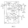
- FIG. 5 shows a fourth preferred embodiment of the present invention.
- the dual-output regulator 100 comprises a PNP power transistor 112 for regulating VDDQ voltage 116 , and two NPN power transistors 127 and 133 for regulating VTT voltage 134 .
- Regulator 100 can be implemented with a bipolar silicon fabrication process.
- PNP transistor 112 The input (emitter) terminal of PNP transistor 112 is connected to input voltage 111 via VIN pin 101 .
- the output (collector) terminal of PNP transistor 112 is connected to VDDQ pin 102 .
- the base current for PNP transistor 112 is drained to ground with the control of OP-AMP 113 .
- PNP transistor 112 is capable of providing a low dropout voltage of less than 500 mV at 5A of output current.
- a voltage divider comprising resistors 114 and 115 is connected to the non-inverting input of OP-AMP 113 via ADJ pin 103 . As described in FIG. 2 , this ADJ pin 103 is also connected to the shutdown input 118 via an isolating diode 117 . The internal ground of regulator 100 is connected to an external ground via a GND pin 104 .
- NPN transistor 127 The input (collector) of NPN transistor 127 is connected to VDDQ pin 102 internally.
- the output (emitter) of NPN transistor 127 sources current to VTT voltage 134 via VTT pin 105 .
- a second NPN transistor 126 supplies the base current of NPN transistor 127
- OP-AMP 124 supplies the base current of NPN transistor 126 via a base resistor 125 .
- OP-AMP 124 can easily support this voltage, with input voltage 111 supplying a 3.3V operating voltage to OP-AMP 124 .
- NPN transistor 133 The input (collector) terminal of NPN transistor 133 is connected to VTT pin 105 internally.
- the output (emitter) terminal of NPN transistor 133 is connected to ground.
- a second PNP transistor 132 supplies the base current of NPN transistor 133
- OP-AMP 124 controls the base current of PNP transistor 132 via a base resistor 131 .
- a single OP-AMP 124 controls both Darlington pairs 126 – 127 and 132 – 133 .
- OP-AMP 124 is operated at 3.3V. Its output voltage range is between 0.2V and 3.1V or better.
- OP-AMP 124 needs an output voltage slightly higher than 2.65V.
- OP-AMP 124 needs an output voltage of slightly lower than 0.55V.
- An internal voltage divider comprising resistors 121 and 122 of a same resistance value, provides a reference voltage 123 of exactly 50% of VDDQ voltage 116 to the positive input of OP-AMP 124 .
- the inverting input of OP-AMP 124 is connected internally to VTT pin 105 . Since OP-AMP 124 has a high DC gain, it will force VTT voltage 134 to follow the reference voltage 123 , which is exactly one half of VDDQ voltage 116 .
- VTT voltage 134 When VTT voltage 134 is trying to drop below 50% of VDDQ voltage 116 , such as in the case of a data bus system drawing more current from VTT voltage 134 , the output voltage of OP-AMP 124 starts to increase. As soon as the output voltage of OP-AMP 124 reaches 0.55V, Darlington pair 132 – 133 turns off. As the voltage has risen to approximately 2.65V, Darlington pair 126 – 127 starts to turn on, thus supplying more current to VTT voltage 134 and restoring VTT voltage 134 quickly to 50% of VDDQ voltage 116 .
- VTT voltage 134 When VTT voltage 134 is trying to rise above 50% of VDDQ voltage 116 , such as in the case of a data bus system returning current to VTT voltage 134 , the output voltage of OP-AMP 124 starts to decrease from a high level to a low level. As soon as the output voltage of OP-AMP 124 drops below 2.65V, Darlington pair 126 – 127 turns off. As the voltage has dropped to approximately 0.55V, Darlington pair 132 – 133 starts to turn on, thus sinking more current from VTT voltage 134 , and quickly restoring VTT voltage 134 to 50% of VDDQ voltage 116 level.
- Each LDO provides a VDDQ voltage or a VTT voltage via at least one transistor (i.e., MOSFET or BJT) and at least one operational amplifier.
- the VTT voltage is half of the VDDQ voltage, saving the cost of the package and capable of using small PCB.
Abstract
Description
Claims (33)
Applications Claiming Priority (2)
| Application Number | Priority Date | Filing Date | Title |
|---|---|---|---|
| TW91123252 | 2002-10-09 | ||
| TW91123252A TW569237B (en) | 2002-10-09 | 2002-10-09 | Dual-output voltage regulator |
Publications (2)
| Publication Number | Publication Date |
|---|---|
| US20040070276A1 US20040070276A1 (en) | 2004-04-15 |
| US7057310B2 true US7057310B2 (en) | 2006-06-06 |
Family
ID=32067578
Family Applications (1)
| Application Number | Title | Priority Date | Filing Date |
|---|---|---|---|
| US10/377,781 Expired - Fee Related US7057310B2 (en) | 2002-10-09 | 2003-03-04 | Dual-output voltage regulator |
Country Status (2)
| Country | Link |
|---|---|
| US (1) | US7057310B2 (en) |
| TW (1) | TW569237B (en) |
Cited By (11)
| Publication number | Priority date | Publication date | Assignee | Title |
|---|---|---|---|---|
| US20060145676A1 (en) * | 2003-08-15 | 2006-07-06 | Atmel Germany Gmbh | Method and circuit arrangement for a power supply |
| US20070001749A1 (en) * | 2005-06-29 | 2007-01-04 | Da-Chun Wei | Dual loop voltage regulation circuit of power supply chip |
| US20070090815A1 (en) * | 2005-10-24 | 2007-04-26 | Faraday Technology Corp. | Integrated circuit with power gating function |
| US20070194771A1 (en) * | 2003-08-20 | 2007-08-23 | Broadcom Corporation | Power management unit for use in portable applications |
| US20070210726A1 (en) * | 2006-03-10 | 2007-09-13 | Standard Microsystems Corporation | Current limiting circuit |
| US20080265683A1 (en) * | 2007-04-27 | 2008-10-30 | Dell Products, Lp | Method and circuit to output adaptive drive voltages within information handling systems |
| US20090021189A1 (en) * | 2007-07-19 | 2009-01-22 | Dubose Garry | Output power port management control |
| US20090128108A1 (en) * | 2007-10-22 | 2009-05-21 | Kabushiki Kaisha Toshiba | Constant voltage power supply circuit |
| US20110019446A1 (en) * | 2009-07-22 | 2011-01-27 | Bcd Semiconductor Manufacturing Limited | Method and apparatus for a switching mode power supply |
| US20130328588A1 (en) * | 2012-06-08 | 2013-12-12 | Hon Hai Precision Industry Co., Ltd. | Testing circuit and printed circuit board using same |
| US20140145691A1 (en) * | 2012-11-27 | 2014-05-29 | Miten H. Nagda | Method and integrated circuit that provides tracking between multiple regulated voltages |
Families Citing this family (6)
| Publication number | Priority date | Publication date | Assignee | Title |
|---|---|---|---|---|
| DE10101744C1 (en) * | 2001-01-16 | 2002-08-08 | Siemens Ag | Electronic switching device and operating method |
| GB0708733D0 (en) * | 2007-05-04 | 2007-06-13 | Nokia Corp | A device |
| CN102623061A (en) * | 2012-03-27 | 2012-08-01 | 上海宏力半导体制造有限公司 | Voltage stabilizing circuit for inhibition voltage of storage |
| CN102710130B (en) * | 2012-05-30 | 2017-10-10 | 西安航天民芯科技有限公司 | A kind of high-precision A C/DC converter current-limiting circuits |
| US10698432B2 (en) | 2013-03-13 | 2020-06-30 | Intel Corporation | Dual loop digital low drop regulator and current sharing control apparatus for distributable voltage regulators |
| IT201900003331A1 (en) * | 2019-03-07 | 2020-09-07 | St Microelectronics Srl | VOLTAGE REGULATOR CIRCUIT AND CORRESPONDING PROCEDURE |
-
2002
- 2002-10-09 TW TW91123252A patent/TW569237B/en not_active IP Right Cessation
-
2003
- 2003-03-04 US US10/377,781 patent/US7057310B2/en not_active Expired - Fee Related
Cited By (23)
| Publication number | Priority date | Publication date | Assignee | Title |
|---|---|---|---|---|
| US20060145676A1 (en) * | 2003-08-15 | 2006-07-06 | Atmel Germany Gmbh | Method and circuit arrangement for a power supply |
| US7746046B2 (en) * | 2003-08-20 | 2010-06-29 | Broadcom Corporation | Power management unit for use in portable applications |
| US20070194771A1 (en) * | 2003-08-20 | 2007-08-23 | Broadcom Corporation | Power management unit for use in portable applications |
| US20100327826A1 (en) * | 2003-08-20 | 2010-12-30 | Broadcom Corporation | Power Management Unit for Use in Portable Applications |
| US20070001749A1 (en) * | 2005-06-29 | 2007-01-04 | Da-Chun Wei | Dual loop voltage regulation circuit of power supply chip |
| US7193453B2 (en) * | 2005-06-29 | 2007-03-20 | Leadtrend Technology Corp. | Dual loop voltage regulation circuit of power supply chip |
| US20070090815A1 (en) * | 2005-10-24 | 2007-04-26 | Faraday Technology Corp. | Integrated circuit with power gating function |
| US20070210726A1 (en) * | 2006-03-10 | 2007-09-13 | Standard Microsystems Corporation | Current limiting circuit |
| US7816897B2 (en) | 2006-03-10 | 2010-10-19 | Standard Microsystems Corporation | Current limiting circuit |
| US20080265683A1 (en) * | 2007-04-27 | 2008-10-30 | Dell Products, Lp | Method and circuit to output adaptive drive voltages within information handling systems |
| US7755215B2 (en) * | 2007-04-27 | 2010-07-13 | Dell Products, Lp | Method and circuit to output adaptive drive voltages within information handling systems |
| US8207628B2 (en) * | 2007-07-19 | 2012-06-26 | Igo, Inc. | Output power port management control |
| US7781908B2 (en) * | 2007-07-19 | 2010-08-24 | Igo, Inc. | Output power port management control |
| US20100308652A1 (en) * | 2007-07-19 | 2010-12-09 | Igo, Inc. | Output power port management control |
| US20090021189A1 (en) * | 2007-07-19 | 2009-01-22 | Dubose Garry | Output power port management control |
| US7859235B2 (en) | 2007-10-22 | 2010-12-28 | Kabushiki Kaisha Toshiba | Constant voltage power supply circuit |
| US20090128108A1 (en) * | 2007-10-22 | 2009-05-21 | Kabushiki Kaisha Toshiba | Constant voltage power supply circuit |
| US20110019446A1 (en) * | 2009-07-22 | 2011-01-27 | Bcd Semiconductor Manufacturing Limited | Method and apparatus for a switching mode power supply |
| US8971060B2 (en) * | 2009-07-22 | 2015-03-03 | Bcd Semiconductor Manufacturing Limited | Method and apparatus for controlling a switching mode power supply during transition of load conditions to minimize instability |
| US20130328588A1 (en) * | 2012-06-08 | 2013-12-12 | Hon Hai Precision Industry Co., Ltd. | Testing circuit and printed circuit board using same |
| US9322873B2 (en) * | 2012-06-08 | 2016-04-26 | Fu Tai Hua Industry (Shenzhen) Co., Ltd. | Testing circuit and printed circuit board using same |
| US20140145691A1 (en) * | 2012-11-27 | 2014-05-29 | Miten H. Nagda | Method and integrated circuit that provides tracking between multiple regulated voltages |
| US8841892B2 (en) * | 2012-11-27 | 2014-09-23 | Freescale Semiconductor, Inc. | Method and integrated circuit that provides tracking between multiple regulated voltages |
Also Published As
| Publication number | Publication date |
|---|---|
| TW569237B (en) | 2004-01-01 |
| US20040070276A1 (en) | 2004-04-15 |
Similar Documents
| Publication | Publication Date | Title |
|---|---|---|
| US7057310B2 (en) | Dual-output voltage regulator | |
| US7683592B2 (en) | Low dropout voltage regulator with switching output current boost circuit | |
| EP1932070B1 (en) | Voltage regulator with low dropout voltage | |
| US7616456B2 (en) | Apparatus and system for providing transient suppression power regulation | |
| EP1365302B1 (en) | Low drop-out voltage regulator | |
| US5867015A (en) | Low drop-out voltage regulator with PMOS pass element | |
| US6703813B1 (en) | Low drop-out voltage regulator | |
| CN111033431B (en) | On-chip NMOS (N-channel metal oxide semiconductor) capacitor-free LDO (low dropout regulator) for high-speed microcontroller | |
| US8026708B2 (en) | Voltage regulator | |
| EP0715238B1 (en) | Circuit and method for regulating a voltage | |
| US7586364B2 (en) | Power supply voltage controlling circuit and semiconductor integrated circuit | |
| US11281244B2 (en) | Output current limiter for a linear regulator | |
| WO2016022861A1 (en) | Short-circuit protection for voltage regulators | |
| EP1508078A2 (en) | Voltage regulator with dynamically boosted bias current | |
| US9977441B2 (en) | Low dropout regulator and related method | |
| EP3933543A1 (en) | Low-dropout regulator for low voltage applications | |
| CN111488028A (en) | Method of forming semiconductor device | |
| US6437638B1 (en) | Linear two quadrant voltage regulator | |
| US8085006B2 (en) | Shunt regulator | |
| JP3852399B2 (en) | Power switching circuit | |
| KR20010106448A (en) | Driver circuit | |
| CN111596719A (en) | High-voltage low dropout regulator (LDO) circuit with reverse connection prevention function | |
| US20230280774A1 (en) | Ldo output power-on glitch removal circuit | |
| CN117155373A (en) | Fast transient buffer | |
| CN115437443A (en) | Low dropout linear voltage stabilizing circuit and system on chip |
Legal Events
| Date | Code | Title | Description |
|---|---|---|---|
| AS | Assignment |
Owner name: ARQUES TECHNOLOGY, TAIWAN Free format text: ASSIGNMENT OF ASSIGNORS INTEREST;ASSIGNORS:LIU, KWANG H.;NEGRU, SORIN L.;GROOM, TERRY;AND OTHERS;REEL/FRAME:013864/0360;SIGNING DATES FROM 20030128 TO 20030205 |
|
| REMI | Maintenance fee reminder mailed | ||
| AS | Assignment |
Owner name: JPMORGAN CHASE BANK, N.A., AS COLLATERAL AGENT,NEW Free format text: SECURITY AGREEMENT;ASSIGNOR:CALIFORNIA MICRO DEVICES CORPORATION;REEL/FRAME:024079/0097 Effective date: 20100225 Owner name: JPMORGAN CHASE BANK, N.A., AS COLLATERAL AGENT, NE Free format text: SECURITY AGREEMENT;ASSIGNOR:CALIFORNIA MICRO DEVICES CORPORATION;REEL/FRAME:024079/0097 Effective date: 20100225 |
|
| LAPS | Lapse for failure to pay maintenance fees | ||
| STCH | Information on status: patent discontinuation |
Free format text: PATENT EXPIRED DUE TO NONPAYMENT OF MAINTENANCE FEES UNDER 37 CFR 1.362 |
|
| FP | Expired due to failure to pay maintenance fee |
Effective date: 20100606 |