US7095494B2 - Method and apparatus for measuring temporal response characteristics of digital mirror devices - Google Patents
Method and apparatus for measuring temporal response characteristics of digital mirror devices Download PDFInfo
- Publication number
- US7095494B2 US7095494B2 US10/230,756 US23075602A US7095494B2 US 7095494 B2 US7095494 B2 US 7095494B2 US 23075602 A US23075602 A US 23075602A US 7095494 B2 US7095494 B2 US 7095494B2
- Authority
- US
- United States
- Prior art keywords
- micromirror array
- photodetector
- response
- light
- diffraction pattern
- Prior art date
- Legal status (The legal status is an assumption and is not a legal conclusion. Google has not performed a legal analysis and makes no representation as to the accuracy of the status listed.)
- Expired - Lifetime, expires
Links
Images


Classifications
-
- G—PHYSICS
- G02—OPTICS
- G02B—OPTICAL ELEMENTS, SYSTEMS OR APPARATUS
- G02B26/00—Optical devices or arrangements for the control of light using movable or deformable optical elements
- G02B26/08—Optical devices or arrangements for the control of light using movable or deformable optical elements for controlling the direction of light
- G02B26/0816—Optical devices or arrangements for the control of light using movable or deformable optical elements for controlling the direction of light by means of one or more reflecting elements
- G02B26/0833—Optical devices or arrangements for the control of light using movable or deformable optical elements for controlling the direction of light by means of one or more reflecting elements the reflecting element being a micromechanical device, e.g. a MEMS mirror, DMD
-
- G—PHYSICS
- G01—MEASURING; TESTING
- G01M—TESTING STATIC OR DYNAMIC BALANCE OF MACHINES OR STRUCTURES; TESTING OF STRUCTURES OR APPARATUS, NOT OTHERWISE PROVIDED FOR
- G01M11/00—Testing of optical apparatus; Testing structures by optical methods not otherwise provided for
- G01M11/005—Testing of reflective surfaces, e.g. mirrors
Definitions
- Micromechanical devices are small structures typically fabricated on a semiconductor wafer using techniques such as optical lithography, metal sputtering, plasma oxide deposition, and plasma etching that have been developed for the fabrication of integrated circuits.
- Digital micromirror devices sometimes referred to as deformable mirror devices, are a type of micromechanical device. Other types of micromechanical devices include accelerometers, pressure and flow sensors, gears and motors.
- Digital micromirror devices are primarily used in optical display systems. In display systems, the DMD is a light modulator that uses digital image data to modulate a beam of light by selectively reflecting portions of the beam of light to a display screen. While analog modes of operation are possible, DMDs are often operated in a digital bistable mode of operation and as such are the core of true digital full-color image projection systems.
- micromirror devices including torsion beam devices, and hidden-hinge devices. All micromirror devices, however, are usually operated in one of two modes of operation.
- the first mode of operation is an analog mode, sometimes called beam steering, wherein the address electrode is charged to a voltage corresponding to the desired deflection of the mirror.
- Light striking the micromirror device is reflected by the mirror at an angle determined by the deflection of the mirror.
- the cone of light reflected by an individual mirror is directed to fall outside the aperture of a projection lens, partially within the aperture, or completely within the aperture of the lens.
- the reflected light is focused by the lens onto an image plane, with each individual mirror corresponding to a pixel on the image plane. As the cone of reflected light is moved from completely within the aperture to completely outside the aperture, the image location corresponding to the mirror dims, creating continuous brightness levels.
- the second mode of operation is a digital mode.
- each micromirror When operated digitally, each micromirror is fully deflected in either of the two directions about the torsion hinge axis.
- Digital operation uses a relatively large address voltage to ensure the mirror is fully deflected.
- the address electrodes are driven using standard logic voltage levels and a bias voltage, typically a positive voltage, is applied to the mirror metal layer to control the voltage difference between the address electrodes and the mirrors.
- a sufficiently large mirror bias voltage a voltage above what is termed the threshold voltage of the device, ensures the mirror will fully deflect toward the address electrode—even in the absence of an address voltage.
- the use of a large mirror bias voltage enables the use of low address voltages since the address voltages need only slightly deflect the mirror prior to the application of the large mirror bias voltage.
- the light source is positioned at an angle relative to the device normal that is twice the angle of rotation so that mirrors rotated toward the light source reflect light in a direction normal to the surface of the micromirror device and into the aperture of a projection lens—creating a bright pixel on the image plane.
- Mirrors rotated away from the light source reflect light away from the projection lens—leaving the corresponding pixel dark.
- Intermediate brightness levels are created by pulse width modulation techniques in which the mirror rapidly is rotated on and off to vary the quantity of light reaching the image plane.
- the human eye integrates the light pulses and the brain perceives a flicker-free intermediate brightness level.
- the temporal response of micromirrors in the micromirror array to input signals is an important metric of the performance of the micromirrors.
- the temporal response characteristics can be used to determine if the micromirrors are operating properly or improperly. More specifically, the temporal response characteristics can detect manufacturing defects in the micromirrors at a macroscopic scale. The characteristics can also measure imperfections and performance variations across the surface of a micromirror array.
- MMDCU micromirror device characterization unit
- Nanospec measuring tool Existing systems for measuring the temporal response of micromirror arrays utilize devices that measure the performance of individual micromirrors in the micromirror array. For example, one method for measuring the temporal response of a micromirror uses a micromirror device characterization unit (MMDCU) or Nanospec measuring tool. These measurement tools have significant drawbacks though. In particular, the tools are expensive, highly sensitive, and require precise alignment with the micromirror array in order to produce accurate measurements. Furthermore, these tools can only measure one mirror at a time, thus producing measurement that have a relatively low signal to noise ratio.
- MMDCU micromirror device characterization unit
- Nanospec measuring tool have significant drawbacks though. In particular, the tools are expensive, highly sensitive, and require precise alignment with the micromirror array in order to produce accurate measurements. Furthermore, these tools can only measure one mirror at a time, thus producing measurement that have a relatively low signal to noise ratio.
- the system utilizes a coherent light source, such as a laser, to illuminate a portion of a micromirror array so that a diffraction pattern is reflected by the micromirror array onto a reflection screen.
- a coherent light source such as a laser
- Diffraction pattern theory dictates that as the micromirrors of the micromirror array are tilted to new angles in unison, the intensity, but not the location, of the spots of the diffraction pattern will change.
- Photodetectors can therefore be aligned with certain spots in the diffraction pattern so that the intensity of these spots can be accurately measured as the micromirrors are tilted to different angles in unison.
- a system may be connected to the micromirror array and to the photodetectors to drive the micromirror array with input signals and measure its response characteristics.
- a DC power supply applies a bias voltage to the micromirror array so that the micromirrors are tilted at an angle (i.e. an operating point) that will produce a large response when they are simultaneously excited by a relatively small AC driving signal.
- a variety of driving signals can be applied to the micromirror array, including, for example, a periodic sinusoidal waveform, a square wave signal, an impulse (i.e. Dirac function) signal, and a frequency swept periodic waveform. By using these different waveforms, a variety of characteristics of the micromirror array can be measured, such as the impulse response, the forced resonant frequency (i.e.
- the electromechanical compliance of the micromirrors in the micromirror array can also be measured.
- Another aspect of the disclosed invention is the measurement of the tilt angle of the micromirror array at a non-biased state. It is further contemplated that all of these measurements can be localized to specific regions on the surface of the micromirror array so that the variance of different parameters across its surface can be analyzed.
- FIG. 1 is block diagram of one embodiment of a temporal measurement system suitable for use with the disclosed method and apparatus.
- FIG. 1A is block diagram of another embodiment of a temporal measurement system suitable for use with the disclosed method and apparatus.
- FIG. 2 is a diffraction pattern that is created by a micromirror array in which all of the mirrors have been placed at the same tilt angle and which has been illuminated with a coherent light source.
- FIG. 3 is a chart depicting a representative example of the response of a micromirror array when two photodetectors are disposed at corresponding diffraction orders and the micromirrors are swept across a variety of tilt angles.
- FIG. 4 is a chart depicting a representative example of the response of a micromirror array in which a photodetector 125 is located at the zeroth diffraction order.
- FIG. 5 is a chart depicting a representative example of the response of a micromirror array to an impulse driving signal.
- FIG. 6 is a chart depicting a representative example of the frequency response of a micromirror array subjected to a periodic driving signal.
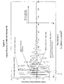
- FIG. 7 is a chart depicting a representative example of a set of electromechanical compliance measurements taken over the entire surface of a micromirror array.
- FIG. 8 is a chart depicting a representative example of the response of a micromirror array that is released from its respective landing positions.
- FIG. 8A is a chart depicting a close-up view of a portion of the response of a micromirror array after the micromirrors have been released from their respective landing positions.
- FIG. 9 is a chart depicting a representative example of the oscillation of a micromirror array after the micromirrors have been released from their respective landing positions.
- FIG. 10 is a top view of a representative micromirror according to one aspect of the invention.
- FIG. 10P is a cross-sectional view of the micromirror depicted in FIG. 10 according to another aspect of the invention.
- FIG. 11A is top-view of a portion of a representative micromirror array suitable for use with the disclosed invention.
- FIG. 11B is a representative view of the geometry and arrangement of the diffraction pattern generated by reflecting a laser beam from the surface of a micromirror array, such as the array depicted in FIG. 11A .
- Micromirrors like any other mechanical system, can be modeled using second order differential equations.
- the transient response of a mechanical mass-spring-damper system can be modeled using the following equation:
- Equation (1.2) represents the Laplace transform of equation (1.1), which places equation (1.1) in the frequency domain:
- the expression for the angular plane wave spectrum (similar to the far-field pattern) generated by a micromirror array when it is illuminated by a collimated laser beam with all mirrors landed in the same direction at tilt angle ⁇ , takes the form:
- (m,n) are the diffraction order indices
- W denotes the “waist” of the illuminating laser (assumed to have a Gaussian profile)
- ⁇ and ⁇ ′ denote the azimuthal and elevational angles respectively
- ⁇ denotes the mirror tilt angle
- k d denotes the “fill factor” of the mirrors
- T denotes the mirror “pitch” (period from one mirror to the next adjacent mirror)
- ⁇ is the wavelength of the laser illumination.
- the exponential (exp) Gaussian terms result from the assumption of Gaussian profiled laser illumination (recall that the Fourier transform of a Gaussian distribution is ALSO a Gaussian). Although this form assumes that the illuminating light is normally incident, it can be easily generalized to treat the case of oblique incidence. This form also ignores minor second order effects such as obliquity factors and geometric distortion factors (i.e. as a mirror tilts, the initially square profile of the mirror assumes an apparent slight “diamond-shape” aspect); but these effects are insignificant for the paraxial conditions associated with most DMDs where landed tilt angles are small, typically on the order of ⁇ 10°.
- the intensity of the reflected laser beam will be the most significant variable in these equations.
- the intensity of the reflected laser beam varies as the modulus squared of the product of the two terms above.
- the photodetector converts the incident light power to a voltage that is proportional to the incident intensity.
- the “k th ” on-diagonal order is blazed when ⁇ k ⁇ /( ⁇ square root over (2) ⁇ T)
- V b (t) V bo + ⁇ cos( ⁇ t).
- a photodetector can be placed on a particular order, which will detect all of the light impinging on that particular order.
- I o , K 1 and K 2 are constants. These values can be varied by choice of a particular operating point (i.e. by choosing ⁇ o ), and by increasing or decreasing excitation amplitude (which controls ⁇ ′). These constants control the relative amplitude of the DC, fundamental (K 1 ) and double frequency (K 2 ) responses.
- FIG. 1 A representative example of an improved measurement system 100 suitable for use with the disclosed invention is depicted in FIG. 1 .
- a coherent light source 105 such as a laser, generates a beam of coherent light 115 that is directed towards the surface of a micromirror array 110 .
- the micromirror array 110 reflects the beam of light 115 and generates a set of reflected light beams 117 . These reflected light beams 117 are directed to a reflection screen 120 .
- the micromirror array 110 is comprised of a periodic array of micromirrors, the reflected light beams 117 form a periodic diffraction pattern of discrete spots (or “diffraction orders”) on the reflection screen 120 .
- An example of a typical diffraction pattern generated by a micromirror array 110 is depicted in FIG. 2 .
- a series of spots 200 are depicted in a pattern corresponding to the diffraction pattern generated by the micromirror array 125 .
- the pattern includes a first spot 205 corresponding to a beam of light that was reflected from the surface of the micromirror array 110 at an angle equal to the angle of incidence of the incoming light beam 115 . Accordingly, the first spot 205 corresponds to a “zeroth order” diffraction point.
- Also depicted in FIG. 2 are a series of spots, 210 , 215 , 220 , 230 and 235 , that are arranged on a line that passes through the first spot 205 . Each of the spots 210 – 235 corresponds to increasing diffraction orders, respectively.
- spot 210 corresponds to a first diffraction order
- spot 215 corresponds to a second diffraction order
- each of these spots 210 – 235 are angularly separated by intervals of approximately ⁇ /T, where ⁇ is the wavelength of the light beam 110 and T is the mirror pitch/spacing.
- a plurality of other spots 260 corresponding to the diffraction pattern are also depicted in FIG. 2 .
- spot 235 is depicted as having a greater intensity than the other spots.
- spots 240 – 255 are depicted as having greater intensity than most of the other spots.
- One or more photodetectors 125 may be placed in the plane of the reflection screen 120 so that they can measure the intensity of the light reflected from the micromirror array.
- each of these photodetectors 125 is aligned with a spot of light corresponding to a respective diffraction order in the diffraction pattern.
- a photodetector 125 may be aligned with a spot of light 210 corresponding to the first diffraction order in the diffraction pattern.
- a second photodetector 125 may be aligned with a spot 212 located on the other side of spot 205 that also corresponds to the first diffraction order.
- FIG. 3 is a diagram depicting the amount of light measured at each of the photodetectors 125 in the arrangement described above as the mirrors in the micromirror array are swept from one parked position to another. Initially, as the mirrors are parked at angle ⁇ , both photodetectors register a minimum amount of light I min . As the mirrors are swept through angle ⁇ 1 , however, the amount of light measured at one of the photodetectors (A) rises to level I max . This corresponds to the rising intensity of the light as the tilt angle of the mirrors changes. After passing through angle ⁇ 1 , the intensity of light measured at photodetector (A) falls level I min .
- the amount of light measured at the other photodetector (B) rises to level I max . This corresponds to the rising intensity of the light as the tilt angle of the mirrors changes. After passing through angle + ⁇ 1 , the intensity of light measured at photodetector (B) falls back to level I min .
- FIG. 4 is a depiction of a chart 400 demonstrating the response of a micromirror array in which a photodetector 125 is located at the zeroth diffraction order.
- a first response curve 405 is depicted that corresponds to the intensity of light at the zeroth diffraction order as the micromirrors in the micromirror array 110 are swept from a angle of ⁇ 2 degrees to +2 degrees.
- the first response curve 405 appropriately has a peak that occurs when the micromirror tilt angle is at zero.
- 2 ⁇ ′ is the peak to peak excursion about point A 1 .
- a second response curve 410 is depicted in FIG. 4 that represents the derivative of the first response curve 405 .
- the second response curve 410 has a peak and a minimum where the slope of the first response curve is greatest; namely, points A 1 and A 2 .
- a third response curve 415 is also depicted in FIG. 4 that represents the second derivative of the first response curve 405 .
- FIG. 1 A system for applying driving signals to the micromirror array 110 and measuring the amount of light reflected by the micromirror array 110 is further depicted in FIG. 1 .
- the photodetectors 125 produce signals corresponding to the intensity of light at their respective locations on the reflection screen 120 . These signals are fed into the digital scope 130 , where they may be displayed and measured.
- the digital scope comprises a digital oscilloscope with display measurement capabilities.
- a function generator 135 that can produce a variety of driving signals including, for example, sinusoidal wave forms, step function wave forms, impulse function wave forms, or saw-tooth patterns. The output of the function generator is fed into a signal summer 142 .
- the function generator 135 can also provide a sync line 165 to the digital scope 130 so that the operations of the function generator 135 can be synchronized with the operations of the digital scope 130 .
- a DC power supply 145 can be used to provide a DC bias signal to the signal summer 142 so that the driving signal generated by the function generator 135 is offset at a particular bias point. After these signals have been combined by the signal summer 142 , they are provided to the micromirror array 110 where they function as a micromirror diving signal.
- the output of the signal summer 142 can also be provided to a personal computer (PC) 160 for other measurements.
- the PC 160 can also be connected to the digital scope 130 for additional measurements. By monitoring the signal that is provided to the micromirror array 110 and by monitoring the measurements performed by the digital scope 130 , the PC can measure a variety of the performance characteristics of the micromirror array 110 .
- FIG. 1A An alternative embodiment of the temporal measurement system is depicted in FIG. 1A .
- the alternative embodiment includes a coherent light source 105 , a micromirror array 110 , a reflector screen 120 , at least one photodetector 125 , a digital scope 130 , a function generator 135 , a DC power supply 145 , and a PC 160 .
- a bias tee 140 Also depicted in FIG. 1A , however, are a bias tee 140 , a reset line break out circuit 150 , a UDE board and voltage board electronics 155 , a dual phase lock-in amplifier 170 , and several additional connections between these components.
- the bias tee 140 combines the signal of the function generator 135 and/or the dual phase lock-in amplifier 170 with the bias voltage provided by the DC power supply 145 to provide a driving signal for the micromirror array 110 .
- the reset line breakout circuit 150 is used to allow various measurements to be conducted on the driving signals that are to be provided to the micromirror array 110 .
- the dual phase lock-in amplifier 170 performs several functions, foremost of these is to provide a periodic signal that can be swept across a variety of frequencies.
- the dual phase lock-in amplifier 170 can also measure the phase differential between its driving signal and the measured response of the micromirror array.
- the dual phase lock-in amplifier 170 can be connected to a PC 160 so that its measurements and calculations can be stored and analyzed.
- the UDE (i.e. Universal Drive Electronics) Board/Voltage Board Electronics are part of the support electronics used to initialize the underlying CMOS to either “ALL ON” or and “ALL OFF” state. Because the CMOS memory in the DMD array normally would power up to an unknown state, the UDE Board is used to write all DMD mirrors to identical states (i.e. either “ALL ON” or “ALL OFF”), so that when the mirror/yokes are driven by the Vbias/reset signal, all mirrors will tilt in unison.
- the temporal measurement system depicted in FIGS. 1 and 1A can be used to measure the impulse response of the micromirrors and the micromirror array.
- the function generator 135 provides the impulse driving signal to the micromirror array.
- the impulse signal can be delivered as a periodic function with a period of sufficient lengths to allow the micromirrors to settle after being driven with an impulse signal. According to another embodiment, however, the impulse signal need not be in the form of a periodic wave, but may instead constitute a single impulse signal.
- a DC bias can be provided by the DC power supply 145 so that the periodic impulse signal is offset to a desired DC bias level. According to a preferred embodiment, the DC bias signal is adjusted until a peak response is measured by the photodetectors 125 .
- a single photodetector 125 is disposed in the plane of the reflector screen 120 so that it is aligned with the zeroth order of the diffraction pattern. By aligning the photodetector 125 with the zeroth order, the measurements are performed closest to the micromirror's resting state.
- An impulse driving signal which can be periodic, is applied to the micromirror array 110 .
- the response of the micromirror array 110 as measured by photodetector 125 is displayed on the digital scope 130 .
- the function generator 135 will generate very narrow pulses (t ⁇ 0.3 microseconds), which is much smaller than the time constant of the mirrors.
- FIG. 5 A chart depicting the measured response of the micromirrors to an impulse signal is depicted in FIG. 5 .
- the response of the micromirror array 110 to an impulse signal with no applied bias is represented by the curve 505 .
- One advantage of the disclosed apparatus in method is the ability to measure the impulse response at a variety of operating points or tilt angles by adjusting the bias voltage of the DC power supply 145 . This concept is depicted in FIG.
- Theoretical models of the impulse response of micromirrors predict that the damped oscillation frequency will decrease as the nominal tilt angle increases.
- the impulse response curves depicted in FIG. 5 correspond to this theory prediction. Specifically, in FIG. 5 , the frequency of the impulse response when the micromirror array is held with zero bias (line 520 ) is much greater than the frequency of the impulse response when the micromirror array 110 is biased with a large voltage (line 505 ).
- the natural frequency (f n ) is a parameter of interest when characterizing the temporal response of a micromirror array 110 .
- the natural frequency (f n ) can be related to the torsional spring constant K and the moment of inertia ( ⁇ ) through the following equation:
- the optical and electrical set-ups used for measuring forced resonant frequency are the same as that used for measuring the impulse response.
- the process begins by sending either an “all-on” or an “all-off” pattern to the micromirror array 110 and placing a photodetector at the zeroth order. It is contemplated, however, that one or more photodetectors 125 may be aligned with orders other than zero, such as, for example, at the first diffraction order.
- the function generator 135 provides a periodic wave form (typically a sinusoidal wave form) through the signal summer 142 to the micromirror array.
- the DC bias applied to the micromirror array can be adjusted so that the largest amplitude response appears on the digital scope 130 . In many instances, this will correspond to the position where the slope of the response curve is greatest, i.e. operating points A 1 or A 2 depicted in FIG. 4 .
- measurements of the forced frequency response can be taken. This is performed by measuring the intensity of light striking the photodetector 125 as the frequency of the driving signal is swept throughout a desired range. The frequency at which the amplitude of the reflected light is greatest is recorded as the natural frequency (f n ) of the micromirrors in the micromirror array 110 .
- FIG. 6 A chart depicting these forced resonant frequency measurements is depicted in FIG. 6 .
- a curve 605 corresponds to the measured intensity of light at the photodetector 125 at a given frequency.
- the measured response curve 605 peaks at approximately 89 kilohertz. Accordingly, the natural frequency of the mirrors in the micromirror array 110 will typically correspond to 89 kilohertz, which is typical for micromirror arrays of this type.
- a curve corresponding to the relative phase shift induced by the application of the periodic driving signal to the micromirror array 110 Measurements of the relative phase shift are described in further detail below.
- a photodetector 125 With the mirrors of the micromirror array 110 landed, a photodetector 125 will typically be placed on a diffraction order that is closest to the blaze point (i.e., the diffraction order that is most strongly illuminated when the mirrors are landed). Much like the previously described process, the frequency is swept over a predetermined range until the amplitude of the measured intensity of light peaks. This measurement of landed micromirror response provides a measure of the spring tip resonance of the micromirror devices.
- the half-power points correspond to frequencies (f 1 and f 2 ) at which the measured AC intensity fluctuation of the reflected light is equal to 1/ ⁇ square root over (2) ⁇ the AC intensity fluctuation of light at the natural frequency.
- the difference between these two half-power points (f 1 and f 2 ) is also known as the bandwidth of the system.
- the bandwidth of the system can be determined by simply measuring the difference between the two half-power points.
- the quality factor (Q) is determined by dividing the natural frequency by the bandwidth of the system.
- the damping factor ⁇ is approximately equal to 1 ⁇ 2Q, which is also equal to (f 2 ⁇ f 1 )/2f n .
- the “damped” resonant frequency (f d ) may be estimated by using the following equation.
- f d f n ⁇ square root over (1 ⁇ 2 ) ⁇
- One advantage of measuring the forced response is that these measurements provide very good signal-to-noise ratio. It should be further noted that these measurements can be performed with the system depicted in FIG. 1A , including using the lock-in amplifier to generate the frequency swept signal and measure the phase of the response (see FIG. 6 ). Measuring the Frequency Transfer Function
- the response measurement system depicted in FIGS. 1 and 1A can also be used to measure the frequency transfer function corresponding to the micromirror array 110 .
- a function generator 135 provides a periodic sinusoidal driving function to drive the micromirror array 110 .
- the dual phase lock-in amplifier 170 provides the periodic sinusoidal driving signal.
- the mirrors in the micromirror array 110 are written to either an “all-on” or “all-off” pattern and the photodetector will be placed at the spot corresponding to the zeroth order.
- the DC bias to be applied to the micromirror array 110 by the DC power supply 145 is adjusted so that the amplitude of the spot intensity is at its greatest. As described previously, this often corresponds to operating points A 1 or A 2 depicted in FIG. 4 . It is contemplated, however, that other arrangements of the system are suitable for measuring the frequency transfer function. For example, one or more photodetectors 125 may be placed on the first, second, or third order, etc. and the DC bias applied by the DC power supply 145 can be greatly varied. According to the embodiment depicted in FIG. 1 A,the dual phase lock-in amplifier 170 sweeps the frequency across a desired range.
- the frequency sweeping function performed by the dual phase lock-in amplifier 170 can be controlled by a visual basic application running on the PC 160 , which sends control signals through the RS232 line to the dual phase lock-in amplifier 170 .
- the lock-in amplifier 170 may use the frequency sweeping output as an internal reference for “sync” detection, such that the relative phase of the response measured by the photodetectors 125 can be measured.
- the magnitude and phase information measured by the dual phase lock-in amplifier 170 is acquired by the PC 160 and the data may be plotted as shown in FIG. 6 .
- curve 605 corresponds to the AC intensity fluctuation of the light measured by the photodetector 125 and the curve 610 corresponds to the relative phase of the signal.
- the half-power points (f 1 and f 2 ), the natural frequency f n , the quality factor (Q), the damping factor ( ⁇ ), and the damped resonate frequency of the micromirror can be calculated.
- the measured data may also be used to determine the transfer function corresponding to the corresponding to the micromirror array 110 .
- the disclosed method and system can also measure electromechanical hinge compliance. This measurement must be distinguished from actual mechanical hinge spring compliance, which is typically measured in degrees tilt per Newton-meter of applied mechanical torque. Instead, electromechanical hinge compliance is measured in units of degrees tilt per applied volt of AC excitation. Actual mechanical hinge spring compliance is much more difficult to accurately measure because of variations in the hinge spacer thickness and hinge sag. Other factors resulting in measurement inaccuracies are a variation in electrostatic force applied to the individual micromirror, which varies nonlinearly, approximately in proportion to the equation 1/d 2 , where d is distance between the low side of the mirror and the corresponding landing electrode.
- Electromechanical compliance is a direct measure of the relative amount of change in mirror tilt angle induced by a known change in applied bias voltage. Because it is a relative metric (i.e. we generally measure “relative” variation, e.g., as a function of position within the die, by spatially scanning across the area of the die), rather than a quantitative metric, its measurement is relatively straightforward.
- an “all-on” or an “all-off” pattern is written to the DMD array with an optical photodetector 125 placed at the zeroth order.
- these operating parameters can be varied so that one or more photodetectors 125 can be aligned with the first, second, third, etc., orders on the diffraction pattern.
- the function generator 135 or a dual phase lock-in amplifier 170 , is used to apply a periodic sinusoidal signal to the micromirror array 110 at a frequency that is well away from the resonant frequency of the micromirror array 110 . It is preferable that the frequency of the driving signal be significantly lower than the resonant frequency.
- the DC bias applied by the DC power supply 145 is adjusted so as to find a bias point at which the amplitude of the measured response is greatest. In many cases, this bias point will correspond to operating points A 1 or A 2 , which are illustrated in FIG. 4 .
- a periodic driving signal (preferably sinusoidal) is applied by the function generator 135 to the micromirror array 110 so that the photodetector(s) measure the response of the micromirrors.
- the amplitude of the response of the micromirror array 110 to the driving signal directly corresponds to the relative electromechanical compliance of the illuminated portion of the micromirror array 110 .
- a motion control stage (not shown in FIGS.
- a chart 700 depicting relative electromechanical compliance measurements taken over the entire surface of a micromirror array 110 is depicted in FIG. 7 .
- Another embodiment of the disclosed method and apparatus can be used to measure the response of a micromirror device 110 as the micromirrors are released from a landed position to a resting position (i.e., a non-biased state). To perform this measurement, all of the mirrors in the micromirror array 110 are landed and then released. This can be done using a simple 24 volt square wave signal. According to the embodiment disclosed in FIG. 1 , the function generator 135 may provide this 24-volt square wave signal. According to another embodiment, the 24-volt square wave signal is provided by a voltage booster circuit that amplifies a much smaller (0–5 volt TTL compatible) signal into a 24-volt square wave signal.
- the actual 24-volt square wave signal should accurately approximate an ideal square wave signal.
- all of the micromirrors in the micromirror array 110 are landed.
- the square volt signal moves from 24 volts to zero, no net external field is applied to the mirrors and they are released from the landing pads. Accordingly, due to the hinge restoration torque, the mirrors travel from the landed site to the non-biased state. Upon reaching the non-biased state, the mirrors will continue to oscillate in a damped oscillatory fashion about the non-biased position. It is also possible to measure the response of the micromirrors as they are released from a landed position to another biased position, such as a tilt angle of 1, 2, 3 or 4 degrees.
- the final resting position of the micromirrors is a tilt angle of several degrees, however, this could correspond to placing a pair of photodetectors 125 at the third and fourth diffraction orders.
- the photodetectors 125 will measure the amount of light reflected by the micromirrors 110 .
- the output response of the photodetectors 125 is displayed at the digital scope 130 and can be measured as a function of time.
- FIG. 8 is a representative example of the response measured by a pair of photodetectors 125 as they are released from the landed position.
- the position and velocity of the micromirrors at specific instances of time can be calculated.
- the acceleration of the mirrors is neglected; however, measurements of the acceleration of the mirrors can be made by analyzing this data with numeric derivatives.
- FIG. 8A depicts the response function when the micromirrors pass by the non-biased state.
- FIG. 8A depicts the response function when the micromirrors pass by the non-biased state.
- FIG. 8A depicts one incident where each photodetector receives a maximum response (corresponding to mirrors tilting in the detector direction) and a zero (corresponding to mirrors being at non-biased state).
- detector 1 indicates a maximum meaning that the micromirrors are tilted in the direction of detector 1 .
- both detector 1 and detector 2 read zero, which indicates that the micromirrors are at the non-biased state.
- detector 2 reads a maximum, which indicates that that micromirrors are tilted in the direction of detector 2 .
- these measurements can also be used to calculate tilt angle of the micromirror array when the mirrors are at the non-biased state.
- the first step of this process is to normalize the response curves of each of the photodetectors to zero. After this is done, with reference to FIG. 8A , the location where the two response curves cross the “zero” line correspond to the time when the micromirrors pass the non-biased state.
- the tilt angle of the micromirrors in the micromirror array at the non-biased state can be measured with a high level of accuracy.
- measurements of the response of the micromirror array can be conducted at operating point B, rather than points A 1 and A 2 (referring to FIG. 4 ).
- the first derivative of the response curve is zero (see curve 410 in FIG. 4 ) and the second derivative is maximal (see curve 415 in FIG. 4 ).
- a driving signal that oscillates about operating point B will excite a harmonic of the fundamental, creating a double frequency response. That is to say, if the DC bias of the measurement system is adjusted so as to lie at operating point B, and an AC sinusoidal signal with frequency f o is supplied as a driving signal, then the photodetector response will contain a strong harmonic signal with frequency 2f o .
- This method can be used to measure the forced resonant frequency of a micromirror array while its mirrors are in a mechanically “neutral” state (i.e. assuming the hinges are not “torque”).
- bladezing i.e. maximally illuminating
- This bias level also known as the “flat voltage,” is an indirect metric for comparing the relative torqueing of various devices.
- the mathematical derivations underlying the principles of this invention are described in further detail below.
- the first set of derivations is based upon a single square mirror that has a hinge that runs diagonally through the mirror.
- a representative embodiment of this mirror is depicted in FIG. 10 .
- a mirror 1000 is depicted with a hinge 1005 that passes diagonally through the mirror 1000 .
- a cross-sectional view of mirror 1000 from point PP is depicted in FIG. 10P .
- the mirror 1000 is deflected at an angle ⁇ from its resting position 1010 .
- the radial position r of a point on the mirror (x o , y o ) is defined by the following formula:
- the depth function d(r, ⁇ ) of a specific point on the mirror (x o , y o ), wherein the depth of the point is measured from the resting position 1010 of the mirror is defined by the following formula:
- E x ⁇ ( x ) 1 T ⁇ comb ⁇ ( x / T ) * ⁇ rect ⁇ [ x k d ⁇ T ] ⁇ exp ⁇ ( - j ⁇ ⁇ 2 ⁇ k ⁇ ⁇ x ⁇ ⁇ sin ⁇ ⁇ ⁇ ) ⁇
- E y ⁇ ( y ) 1 T ⁇ comb ⁇ ( y / T ) * ⁇ rect ⁇ [ y k d ⁇ T ] ⁇ exp ⁇ ( - j ⁇ ⁇ 2 ⁇ k ⁇ ⁇ y ⁇ ⁇ sin ⁇ ⁇ ⁇ ) ⁇ , and where comb
- W is the “waist” of the illumination beam that is determined by how tightly the laser beam is focused before striking the mirror array.
- the Gaussian illumination profile serves to effectively window the otherwise infinite array of mirrors.
- the angular plane wave spectrum generated by that array is of particular interest. This spectrum can be obtained by a simple Fourier transform, then replacing the transform variables (f x , f y ) with (sin ⁇ / ⁇ , sin ⁇ ′/ ⁇ ) respectively. This is made easier by the fact that E(x,y) is separable.
- the following Fourier Transform relations are also useful: F ⁇ exp[ ⁇ (x/W) 2 ] ⁇ square root over ( ⁇ ) ⁇ W exp[ ⁇ ( ⁇ Wf x ) 2 ];
- F ⁇ ⁇ E ⁇ ( x ) ⁇ ⁇ ⁇ W ⁇ ⁇ k d ⁇ T ⁇ ⁇ exp ⁇ [ - ( ⁇ ⁇ ⁇ W ⁇ ⁇ f x ) 2 ] * ⁇ comb ⁇ ( T ⁇ ⁇ f x ) ⁇ sinc [ k d ⁇ T ⁇ ( f x + 2 ⁇ sin ⁇ ⁇ ⁇ ⁇ ) ] ⁇
- F ⁇ E(f y ) ⁇ is identical to this equation, with the exception that f x is replaced with f y . Accordingly, the diffraction pattern may be described by the rightmost term which is periodic, convolved with the Gaussian “point spread function.”
- a ⁇ ⁇ ( ⁇ , ⁇ ′ ) ⁇ ⁇ ( W ⁇ ⁇ k d ⁇ T ) 2 ⁇ X ⁇ ⁇ exp ⁇ [ - ( ⁇ ⁇ ⁇ W ⁇ ⁇ sin ⁇ ⁇ ⁇ / ⁇ ) 2 ] * ⁇ comb ⁇ ( T ⁇ ⁇ sin ⁇ ⁇ ⁇ / ⁇ ) ⁇ sinc ⁇ [ k d ⁇ T ⁇ ⁇ ( sin ⁇ ⁇ ⁇ + 2 ⁇ ⁇ sin ⁇ ⁇ ) ] ⁇ ⁇ X ⁇ ⁇ exp ⁇ [ - ( ⁇ ⁇ ⁇ W ⁇ ⁇ sin ⁇ ⁇ ⁇ ′ / ⁇ ) 2 ] * ⁇ comb ⁇ ( T ⁇ ⁇ sin ⁇ ⁇ ⁇ ′ / ⁇ ) ⁇ sinc ⁇ [ k d ⁇ T ⁇ ⁇ ( sin ⁇ ⁇ ⁇ ′ + 2 ⁇
- a ⁇ ⁇ ′ ⁇ ( ⁇ ′ ) sin ⁇ ⁇ c ⁇ [ k d ⁇ T ⁇ ⁇ ( ⁇ ′ + 2 ⁇ ⁇ sin ⁇ ⁇ ⁇ ) ]
- ⁇ m - ⁇ ⁇ ⁇ ⁇ exp ⁇ [ - ( ⁇ ⁇ ⁇ W ⁇ ) 2 ⁇ ( ⁇ ′ - n ⁇ ⁇ ⁇ T ) 2 ] .
- the period between nulls of the sinc pattern ⁇ /(k d T).
- the comb function determines the periodicity of the diffraction pattern.
- the angular period is ⁇ /T, which is nearly the same as the sinc period, particularly when k d approaches unity. This could result in “beat frequency” effects, whereby various diffraction spots will occasionally fall on the null of the sinc 2 distribution in a predictable manner.
Abstract
Description
wherein f(t) is the applied force, M is the mass, B is the damping coefficient, K is the linear spring constant, and y(t) is the displacement of the system. Micromirrors, which have mass, spring-like mounts, and can have damping forces applied, can therefore be accurately modeled with equations similar to equation (1.1).
By applying well known mathematical theories to this equation, the natural frequency (ωn), and the damping factor (ζ) of the mechanical system can be determined. Furthermore, by analyzing equation (1.2) in the frequency domain, other useful information can be determined, such as the poles and roots of the system. It should also be noted that these calculations can be performed in reverse; namely, by measuring the natural frequency (ωn) and the damping factor (ζ) of the mechanical system, its poles, roots, mass, damping coefficient, and linear spring constant can be determined. In this manner, may useful characteristics of the micromirror array can be measured.
Theoretical Model for the Measurement System
The derivation of these equations is described in further detail in the subsequent section entitled “The Mathematical Model of the Diffraction Pattern.” These equations (1.3), which express the resulting angular plane wave spectrum of the far-field diffraction pattern, result from a wave optics analysis of the DMD array. Here, (m,n) are the diffraction order indices, W denotes the “waist” of the illuminating laser (assumed to have a Gaussian profile), φ and φ′ denote the azimuthal and elevational angles respectively, α denotes the mirror tilt angle, kd denotes the “fill factor” of the mirrors, T denotes the mirror “pitch” (period from one mirror to the next adjacent mirror), and λ is the wavelength of the laser illumination. The “sinc” term arises from the rectangular mirror profile (recall that the Fourier transform of a “rect” function is a “sinc” function, where sinc(x)=sin(πx)/(πx)). The exponential (exp) Gaussian terms result from the assumption of Gaussian profiled laser illumination (recall that the Fourier transform of a Gaussian distribution is ALSO a Gaussian). Although this form assumes that the illuminating light is normally incident, it can be easily generalized to treat the case of oblique incidence. This form also ignores minor second order effects such as obliquity factors and geometric distortion factors (i.e. as a mirror tilts, the initially square profile of the mirror assumes an apparent slight “diamond-shape” aspect); but these effects are insignificant for the paraxial conditions associated with most DMDs where landed tilt angles are small, typically on the order of ±10°.
Ultimately, the intensity of the reflected laser beam will be the most significant variable in these equations. The intensity of the reflected laser beam varies as the modulus squared of the product of the two terms above. The photodetector converts the incident light power to a voltage that is proportional to the incident intensity.
Here the expression has been normalized, i.e. the π(WkdT)2 term has been ignored, and only the non-cross-term products have been retained, replacing the indices i and i2 above, with k=i=i2. The symbol β indicates the on-diagonal angle (see
A photodetector can be placed on a particular order, which will detect all of the light impinging on that particular order. In this case the photodetector signal current generated by a detector placed on the kth (on-diagonal order, where k=m=n) is proportional to the incident light power, and will be given by:
The nonlinearity inherent in the profile of the sinc4 term will naturally cause the detector current to contain a mixture of DC, a fundamental signal component at temporal frequency Ω, as well as harmonics of this signal (2Ω, 3Ω etc.). These signal terms can be found by expanding the sinc4 term out in a Taylor series expansion (with respect to α, centered at α=αo).
i d(t)=i o +C 1(α−αo)+C 2(α−αo)2 +C n(α−αo)n+ . . . ,
Because the sinc4 function is well behaved, and since the system will always be excited with a very small signal, it is sufficient to retain only the first few terms of the Taylor series, giving:
i d(t)≅i o +C 1(α−αo)+C2(α−αo)2. (1.9)
As before, α will be replaced with αo+Δ′ cos(Ωt+γ), giving the following equation:
i d(t)≅i o +C 1Δ′ cos(Ωt+γ)+C 2Δ′2 cos2(Ωt+γ)≅I o +K 1 cos(Ωt+γ)+K 2 cos[2(Ωt+γ)], (1.10)
where the identity cos2(θ)=(½)[1+cos(2θ)], and K1=C1Δ′, K2=C2Δ′2/2, and Io=io(1+C2Δ′2/2)≅io have been utilized.
f d =f n√{square root over (1−ξ2)}
One advantage of measuring the forced response (as opposed to measuring the transient impulse/damped response as described above) is that these measurements provide very good signal-to-noise ratio. It should be further noted that these measurements can be performed with the system depicted in
Measuring the Frequency Transfer Function
Accordingly, the depth function d(r, α) of a specific point on the mirror (xo, yo), wherein the depth of the point is measured from the
Now for the paraxial case (α small) we consider plane wave illumination along the Z axis (i.e. perpendicular to the resting
Λ(x,y)=rect(x/k d T)rect(y/k d T)
wherein T is the pitch (spatial period of the mirrors), kd is the “fill factor” of the mirror, and the “rect” function is defined by:
For nonzero α, the apparent aperture distorts slightly (into more of a “diamond” shape), but for tilt angles of ±12°, this distortion is relatively insignificant and will be disregarded, as will the obliquity factor.
Because this equation is separable, an array of mirrors can be emulated by convolving this equation with a periodic “comb” function, such as the one written below:
E(x,y)=E x(x)E y(y) where:
where comb
and δ(x) is the well-known Dirac delta function.
Finally, a Gaussian equation, which describes the spatial profile of a typical gas laser beam, is utilized as follows:
E(r)=exp[−(r/W)2]=exp[−(x/W)2]exp [−(y/W)2].
It should be noted that this equation is separable, like the functions describing the reflected field of the mirrors. Applying the Gaussian equation to the equations describing the reflected field of the mirrors produces the following equations.
E(x,y)=E x(x)E y(y) where:
In this equation, W is the “waist” of the illumination beam that is determined by how tightly the laser beam is focused before striking the mirror array.
F{exp[−(x/W)2]}→√{square root over (π)} W exp[−(πWfx)2];
Applying these facts and using the convolution theorem gives the following equation:
Because the micromirror array is symmetrical about the X and Y axes, F {E(fy)} is identical to this equation, with the exception that fx is replaced with fy. Accordingly, the diffraction pattern may be described by the rightmost term which is periodic, convolved with the Gaussian “point spread function.” By replacing fx with sin φ/λ etc., the following equation is rendered:
This equation can also be expressed as a periodic array of diffracted Gaussian spots, weighted by a sinc envelope where sinc(x)≡sin(πx)/πx, as:
Ã(φ,φ′)=π(Wk d T)2 Ã φ(φ)Ã φ, (φ′) where:
In these equations, the liberty of making the paraxial approximations sin φ≅φ, sin φ′≅φ′ has been taken. In this particular embodiment, the [sin(x)/x]2 (actually described above in terms of a sinc function, although we understand that sinc(x)=(sin(πx)/πx) distribution moves in a diagonal direction as the tilt angle (a) varies (i.e. it has equal components of displacement in the φ and φ′ directions), whereas in
where φn now represents the horizontal axis and φn′ the vertical axis. We refrain from carrying on this calculation here, in the interest of brevity.
Claims (23)
Priority Applications (1)
| Application Number | Priority Date | Filing Date | Title |
|---|---|---|---|
| US10/230,756 US7095494B2 (en) | 2002-08-29 | 2002-08-29 | Method and apparatus for measuring temporal response characteristics of digital mirror devices |
Applications Claiming Priority (1)
| Application Number | Priority Date | Filing Date | Title |
|---|---|---|---|
| US10/230,756 US7095494B2 (en) | 2002-08-29 | 2002-08-29 | Method and apparatus for measuring temporal response characteristics of digital mirror devices |
Publications (2)
| Publication Number | Publication Date |
|---|---|
| US20040042000A1 US20040042000A1 (en) | 2004-03-04 |
| US7095494B2 true US7095494B2 (en) | 2006-08-22 |
Family
ID=31976578
Family Applications (1)
| Application Number | Title | Priority Date | Filing Date |
|---|---|---|---|
| US10/230,756 Expired - Lifetime US7095494B2 (en) | 2002-08-29 | 2002-08-29 | Method and apparatus for measuring temporal response characteristics of digital mirror devices |
Country Status (1)
| Country | Link |
|---|---|
| US (1) | US7095494B2 (en) |
Cited By (6)
| Publication number | Priority date | Publication date | Assignee | Title |
|---|---|---|---|---|
| US7277173B1 (en) * | 2002-12-24 | 2007-10-02 | Agere Systems Inc. | Active optical alignment using MEMS mirrors |
| US20080059099A1 (en) * | 2006-08-29 | 2008-03-06 | Samsung Electro-Mechanics Co., Ltd. | Apparatus and method for calibrating displacement of reflective parts in diffractive optical modulator |
| WO2008109052A1 (en) * | 2007-03-02 | 2008-09-12 | Olympus Corporation | Display system comprising a mirror device with micromirrors controlled to operate in intermediate oscillating state |
| WO2008109050A1 (en) * | 2007-03-02 | 2008-09-12 | Olympus Corporation | Display system comprising a mirror device with micromirrors controlled to operate in intermediate oscillating state |
| WO2014113118A2 (en) * | 2012-11-01 | 2014-07-24 | Arizona Board Of Regents On Behalf Of The University Of Arizona | Reconfigurable diffractive optical switch |
| US9726827B2 (en) | 2012-11-01 | 2017-08-08 | Arizona Board Of Regents On Behalf Of The University Of Arizona | Reconfigurable diffractive optical switch and method for operating the same |
Families Citing this family (25)
| Publication number | Priority date | Publication date | Assignee | Title |
|---|---|---|---|---|
| US6969635B2 (en) * | 2000-12-07 | 2005-11-29 | Reflectivity, Inc. | Methods for depositing, releasing and packaging micro-electromechanical devices on wafer substrates |
| US7034982B2 (en) * | 2004-04-13 | 2006-04-25 | Reflectivity, Inc | Method of improving the performance of microstructures |
| US7345806B2 (en) * | 2004-06-23 | 2008-03-18 | Texas Instruments Incorporated | Method and apparatus for characterizing microelectromechanical devices on wafers |
| US20050286044A1 (en) * | 2004-06-23 | 2005-12-29 | Andrew Huibers | Method and apparatus for qualitatively analyzing uniformity in microelectromechanical devices |
| US7483126B2 (en) * | 2004-06-23 | 2009-01-27 | Texas Instruments Incorporated | Performance analyses of micromirror devices |
| US7378287B2 (en) * | 2004-06-23 | 2008-05-27 | Texas Instruments Incorporated | Wafer matching methods for use in assembling micromirror array devices |
| US7289256B2 (en) * | 2004-09-27 | 2007-10-30 | Idc, Llc | Electrical characterization of interferometric modulators |
| US7343080B2 (en) * | 2004-09-27 | 2008-03-11 | Idc, Llc | System and method of testing humidity in a sealed MEMS device |
| US7557932B2 (en) * | 2005-04-19 | 2009-07-07 | Texas Instruments Incorporated | Characterization of micromirror array devices using interferometers |
| US7630085B2 (en) * | 2005-04-19 | 2009-12-08 | Texas Instruments Incorporated | Interferometers of high resolutions |
| US20060232784A1 (en) * | 2005-04-19 | 2006-10-19 | Regis Grasser | Interferometers of high resolutions |
| US7847538B2 (en) * | 2006-12-29 | 2010-12-07 | Texas Instruments Incorporated | Testing micromirror devices |
| US7423287B1 (en) | 2007-03-23 | 2008-09-09 | Qualcomm Mems Technologies, Inc. | System and method for measuring residual stress |
| US20090051369A1 (en) * | 2007-08-21 | 2009-02-26 | Qualcomm Incorporated | System and method for measuring adhesion forces in mems devices |
| US8103328B2 (en) * | 2007-10-01 | 2012-01-24 | Quantum Applied Science And Research, Inc. | Self-locating sensor mounting apparatus |
| US8274299B2 (en) * | 2008-02-11 | 2012-09-25 | Qualcomm Mems Technologies, Inc. | Methods for measurement and characterization of interferometric modulators |
| BRPI0907132A2 (en) * | 2008-02-11 | 2015-07-14 | Qualcomm Mems Technologies Inc | Device and method for sensing, measuring or characterizing display elements integrated with the drive and screen scheme |
| WO2009102621A2 (en) * | 2008-02-11 | 2009-08-20 | Qualcomm Mems Technologies, Inc. | Methods for measurement and characterization of interferometric modulators |
| US8027800B2 (en) * | 2008-06-24 | 2011-09-27 | Qualcomm Mems Technologies, Inc. | Apparatus and method for testing a panel of interferometric modulators |
| US8035812B2 (en) * | 2009-03-24 | 2011-10-11 | Qualcomm Mems Technologies, Inc. | System and method for measuring display quality with a hyperspectral imager |
| US10067169B1 (en) * | 2014-11-25 | 2018-09-04 | Sean Andrew Cantrell | Method and apparatus to characterize nonlinear systems via their steady state response |
| US10739670B2 (en) * | 2015-12-04 | 2020-08-11 | Augmency Teknoloji Sanayi Anonim Sirketi | Physical object reconstruction through a projection display system |
| JP6572120B2 (en) * | 2015-12-14 | 2019-09-04 | 浜松ホトニクス株式会社 | Light beam irradiation device |
| CN112484667B (en) * | 2020-11-05 | 2021-11-26 | 中国人民解放军国防科技大学 | Photoelectric angle sensor based on two-dimensional material light absorption structure array |
| CN114576303A (en) * | 2022-03-02 | 2022-06-03 | 西安热工研究院有限公司 | Combined type electromagnetic shock absorber |
Citations (9)
| Publication number | Priority date | Publication date | Assignee | Title |
|---|---|---|---|---|
| US3617755A (en) * | 1969-12-10 | 1971-11-02 | Bell Telephone Labor Inc | Apparatus for locating and measuring the beam-waist radius of a gaussian laser beam |
| US5796508A (en) * | 1996-02-28 | 1998-08-18 | Fuji Photo Film Co., Ltd. | Micromirror type image forming apparatus and administration method for the same |
| US20020079432A1 (en) * | 2000-08-07 | 2002-06-27 | Lee Benjamin L. | Two-dimensional blazed MEMS grating |
| US20020106144A1 (en) * | 2001-02-07 | 2002-08-08 | Garverick Steven L. | Multiplexed analog control system for electrostatic actuator array |
| US20030220749A1 (en) * | 2002-04-09 | 2003-11-27 | Zhongping Chen | Phase-resolved functional optical coherence tomography: simultaneous imaging of the stokes vectors, structure, blood flow velocity, standard deviation and birefringence in biological samples |
| US6744550B2 (en) * | 1999-11-16 | 2004-06-01 | Xros, Inc. | Two-dimensional micro-mirror array enhancements |
| US6775047B1 (en) * | 2002-08-19 | 2004-08-10 | Silicon Light Machines, Inc. | Adaptive bipolar operation of MEM device |
| US6788416B2 (en) * | 2002-05-22 | 2004-09-07 | Texas Instruments Incorporated | Method and apparatus for dynamic DMD testing |
| US6831750B2 (en) * | 2002-05-31 | 2004-12-14 | Texas Instruments Incorporated | Method and apparatus for using spatial patterns for measuring mirror tilt angles in digital mirror devices |
-
2002
- 2002-08-29 US US10/230,756 patent/US7095494B2/en not_active Expired - Lifetime
Patent Citations (9)
| Publication number | Priority date | Publication date | Assignee | Title |
|---|---|---|---|---|
| US3617755A (en) * | 1969-12-10 | 1971-11-02 | Bell Telephone Labor Inc | Apparatus for locating and measuring the beam-waist radius of a gaussian laser beam |
| US5796508A (en) * | 1996-02-28 | 1998-08-18 | Fuji Photo Film Co., Ltd. | Micromirror type image forming apparatus and administration method for the same |
| US6744550B2 (en) * | 1999-11-16 | 2004-06-01 | Xros, Inc. | Two-dimensional micro-mirror array enhancements |
| US20020079432A1 (en) * | 2000-08-07 | 2002-06-27 | Lee Benjamin L. | Two-dimensional blazed MEMS grating |
| US20020106144A1 (en) * | 2001-02-07 | 2002-08-08 | Garverick Steven L. | Multiplexed analog control system for electrostatic actuator array |
| US20030220749A1 (en) * | 2002-04-09 | 2003-11-27 | Zhongping Chen | Phase-resolved functional optical coherence tomography: simultaneous imaging of the stokes vectors, structure, blood flow velocity, standard deviation and birefringence in biological samples |
| US6788416B2 (en) * | 2002-05-22 | 2004-09-07 | Texas Instruments Incorporated | Method and apparatus for dynamic DMD testing |
| US6831750B2 (en) * | 2002-05-31 | 2004-12-14 | Texas Instruments Incorporated | Method and apparatus for using spatial patterns for measuring mirror tilt angles in digital mirror devices |
| US6775047B1 (en) * | 2002-08-19 | 2004-08-10 | Silicon Light Machines, Inc. | Adaptive bipolar operation of MEM device |
Non-Patent Citations (1)
| Title |
|---|
| U.S. Appl. No. 10/160,377, filed May 31, 2002, Mehrl et al. |
Cited By (12)
| Publication number | Priority date | Publication date | Assignee | Title |
|---|---|---|---|---|
| US7277173B1 (en) * | 2002-12-24 | 2007-10-02 | Agere Systems Inc. | Active optical alignment using MEMS mirrors |
| US20080059099A1 (en) * | 2006-08-29 | 2008-03-06 | Samsung Electro-Mechanics Co., Ltd. | Apparatus and method for calibrating displacement of reflective parts in diffractive optical modulator |
| WO2008109052A1 (en) * | 2007-03-02 | 2008-09-12 | Olympus Corporation | Display system comprising a mirror device with micromirrors controlled to operate in intermediate oscillating state |
| WO2008109050A1 (en) * | 2007-03-02 | 2008-09-12 | Olympus Corporation | Display system comprising a mirror device with micromirrors controlled to operate in intermediate oscillating state |
| US20080231936A1 (en) * | 2007-03-02 | 2008-09-25 | Taro Endo | Display system comprising a mirror device with micromirrors controlled to operate in intermediate oscillating state |
| US20080246783A1 (en) * | 2007-03-02 | 2008-10-09 | Taro Endo | Display system comprising a mirror device with micromirrors controlled to operate in intermediate oscillating state |
| WO2008130466A1 (en) * | 2007-03-02 | 2008-10-30 | Olympus Corporation | Display system comprising a mirror device with micromirrors controlled to operate in intermediate oscillating state |
| US7961161B2 (en) | 2007-03-02 | 2011-06-14 | Silicon Quest Kabushiki-Kaisha | Display system comprising a mirror device with micromirrors controlled to operate in intermediate oscillating state |
| WO2014113118A2 (en) * | 2012-11-01 | 2014-07-24 | Arizona Board Of Regents On Behalf Of The University Of Arizona | Reconfigurable diffractive optical switch |
| WO2014113118A3 (en) * | 2012-11-01 | 2014-08-21 | Arizona Board Of Regents On Behalf Of The University Of Arizona | Reconfigurable diffractive optical switch |
| US9453970B2 (en) | 2012-11-01 | 2016-09-27 | The Arizona Board Of Regents On Behalf Of The University Of Arizona | Reconfigurable diffractive optical switch |
| US9726827B2 (en) | 2012-11-01 | 2017-08-08 | Arizona Board Of Regents On Behalf Of The University Of Arizona | Reconfigurable diffractive optical switch and method for operating the same |
Also Published As
| Publication number | Publication date |
|---|---|
| US20040042000A1 (en) | 2004-03-04 |
Similar Documents
| Publication | Publication Date | Title |
|---|---|---|
| US7095494B2 (en) | Method and apparatus for measuring temporal response characteristics of digital mirror devices | |
| US6947189B2 (en) | Apparatus and method for optical raster-scanning in a micromechanical system | |
| US6831750B2 (en) | Method and apparatus for using spatial patterns for measuring mirror tilt angles in digital mirror devices | |
| EP2339390B1 (en) | Method and device for monitoring movement of mirrors in a MEMS device | |
| KR100682955B1 (en) | Apparatus and method for evaluating driving characteristic of scanner | |
| Hart et al. | Stroboscopic interferometer system for dynamic MEMS characterization | |
| US8077324B2 (en) | Surface characteristic determining apparatus | |
| JP4083751B2 (en) | System for calibrating a spatial light modulator array and method for calibrating a spatial light modulator array | |
| Lammel et al. | Tunable optical filter of porous silicon as key component for a MEMS spectrometer | |
| EP3521894B1 (en) | Mems reflector system with trajectory control | |
| JP6846567B2 (en) | Angular magnetic field sensor for scanner | |
| US7812950B2 (en) | System method and apparatus for optical directional determination | |
| JP2009544984A (en) | Gas velocity sensor | |
| US7130058B2 (en) | System and method for determining coordinates on three-dimensional space using beam phase interference | |
| CN117091805A (en) | Scanning mirror test system and method based on two-dimensional PSD | |
| US7345806B2 (en) | Method and apparatus for characterizing microelectromechanical devices on wafers | |
| US20090212874A1 (en) | Oscillator device | |
| Cowan et al. | Optical phase modulation using a refractive lenslet array and micro-electro-mechanical deformable mirror | |
| Rhoadarmer et al. | Interferometric characterization of the flexure-beam micromirror device | |
| JP6961502B2 (en) | Optical scanning device | |
| Shi et al. | Performance of segmented mirror coarse phasing with a dispersed fringe sensor: modeling and simulations | |
| JP4565474B2 (en) | Optical switch and optical switch control method | |
| US20220098028A1 (en) | System and method of continuous, vibration-less, and bi-directional MEMS mirror motion via periodic driving force for rapid data acquisition | |
| JP2003108228A (en) | Positioning apparatus, near-field microscope using the apparatus and near-field spectroscope | |
| KR100611601B1 (en) | Point diffraction interferometer comprising automatic collimator |
Legal Events
| Date | Code | Title | Description |
|---|---|---|---|
| AS | Assignment |
Owner name: TEXAS INSTRUMENTS INCORPORATED, TEXAS Free format text: ASSIGNMENT OF ASSIGNORS INTEREST;ASSIGNORS:MEHRL, DAVID JOSEPH;PAN, KUN CINDY;STRUMPELL, MARK HENRY;AND OTHERS;REEL/FRAME:013255/0280 Effective date: 20020826 |
|
| STCF | Information on status: patent grant |
Free format text: PATENTED CASE |
|
| FPAY | Fee payment |
Year of fee payment: 4 |
|
| FPAY | Fee payment |
Year of fee payment: 8 |
|
| MAFP | Maintenance fee payment |
Free format text: PAYMENT OF MAINTENANCE FEE, 12TH YEAR, LARGE ENTITY (ORIGINAL EVENT CODE: M1553) Year of fee payment: 12 |